36 th International Electronic Manufacturing Technology Conference, 2014 Effect of Microwave Hybrid Heating on the Formation of Intermetallic Compound of Sn-Ag-Cu Solder Joints Maisarah Lutfi 1,2 , Farazila Yusof 1,2 , S. Ramesh 1,2 , T. Ariga 1,3 , M. Hamdi 1,2 1 Department of Mechanical Engineering, Faculty of Engineering, University of Malaya, 50603, Kuala Lumpur, Malaysia 2 Centre of Advanced Manufacturing and Material Processing (AMMP Centre), University of Malaya, 50603, Kuala Lumpur, Malaysia 3 Department of Metallurgical Engineering, School of Engineering, Tokai University, 1117 Kitakaname, Hiratsuka, 259-12, Kanagawa, Japan. *Corresponding author: [email protected]Abstract Microwave hybrid heating (MHH) technique was used for investigate the formation of intermetallic compound layer at Sn-3.0Ag-0.5Cu/Cu interface. 4g and 6g of graphite powder were used as susceptor to provide initial heating of the solder alloy before it starts couple with the microwaves and melted on the Cu surface. The IMCs interface was characterized through Field Emission Scanning Electron Microscope (FESEM), Electron Dispersive X-ray (EDS), X-ray Diffraction (XRD) and nanohardness. Microstructural study showed the formation of Cu6Sn5 and Cu3Sn IMCs at the Sn-3.0Ag-0.5Cu/Cu interface after 120s, 150s and 180s microwave heating time. The Cu6Sn5 IMC scallop-like and angular trapezoid structure are formed after 180s microwave heating time with 4g and 6g of graphite powder respectively. 1. Introduction Solder joints play an important role in microelectronic packaging devices. [1]. As the geometry of electronic products become small and complex, the reliability of solder joints will become more critical issues especially to the long term of products performance. [2]. As replacements for conventional Sn–Pb eutectic solder, Sn–Ag–Cu based alloys are leading lead-free candidate solders for electronic manufacturing application [3] It has the lowest melting temperature compared to Sn-Ag and Sn-Cu based alloys, superior mechanical properties and good solderability [4]. Formation of intermetallic compounds (IMCs) layer between the Sn–Ag–Cu solders and substrate is one of the critical parameter to the reliability of the solder joints [5]. These large IMCs are quite brittle and the thermal mismatch between the solder and the substrate will weaken the solder joint strength and eventually cause the fatigue failure. Adding alloying element in the solder alloys may improved the performance of the interfacial IMCs layer [2]. Another way to minimize the excessive growth of the IMC layer is through faster heating and shortening holding time at the peak temperature in the reflow process [6]. The faster and uniform heating is possible by using microwave energy. The heating mechanism of microwave energy is fundamentally different from conventional furnace heating. Conventional heating involves radiant or resistance heating followed by transfer of thermal energy via conduction to the inside of the body being processed [7]. On the other hand, microwave heating is a volumetric heating involving conversion of electromagnetic energy into thermal energy, which is instantaneous, rapid and highly efficient [8]. Beside that, microwave heating is not only a green manufacturing process but also significantly faster at relatively low cost investment [9]. In late 1980s, there was growing interest in high temperature microwave for processing of materials. It has started with microwave application to polymer, followed by ceramic and recently it is used to heat metallic materials in the form of sintering, coating or cladding and joining processes [9]. Recent literature has shown very limited research in the soldering process of metallic materials by using microwave energy. Successful soldering of the Sn- 3.5Ag and Sn-3.8Ag-0.7Cu on Cu surface using Variable Frequency Microwave (VFM) was reported by Moon et. al [6]. The authors showed that the Cu6Sn5 and Ag3Sn IMCs formed at the solder-pad interface by microwave heating at frequency of 6.425 GHz. The IMCs formed had a larger and coarser structure compared to conventional reflow process. However, no details on characterisation of Sn-3.0Ag- 0.5Cu/Cu interface through domestic microwave oven were reported. In this paper, a domestic microwave oven with frequency 2.45GHz was used to investigate the interfacial reaction of Sn-3.0Ag-0.5Cu joints on a copper substrate. This microwave hybrid heating (MHH) which combining microwave and conventional heating mechanism by using microwave absorber materials (graphite) as susceptor are first reported. The weight of the susceptor and microwave heating times were varied, while the microwave power and amount of solder paste were fixed. The morphologies and mechanical properties of IMCs formation were evaluated and discussed. Principle of Microwave Hybrid Heating (MHH) Microwave hybrid heating is a combination of microwave and conventional heating. MHH involves two types of energy for heating the material; microwave energy and thermal energy from the external sources such as use of a separate conventional heating source or using a microwave susceptor. Microwave susceptor is useful for initial heating due to its ability to absorb electromagnetic energy and convert it to heat. It is to mainly keep the temperature of the samples more uniform and also to provide initial heating of the sample before it starts coupling with the microwaves [10]. The microwave absorbing materials such as silicon carbide or graphite are
Transcript
36th International Electronic Manufacturing Technology Conference, 2014
Effect of Microwave Hybrid Heating on the Formation of Intermetallic Compound of Sn-Ag-Cu Solder Joints
Maisarah Lutfi 1,2 , Farazila Yusof 1,2, S. Ramesh 1,2, T. Ariga 1,3, M. Hamdi1,2
1 Department of Mechanical Engineering, Faculty of Engineering, University of Malaya, 50603, Kuala Lumpur, Malaysia
2 Centre of Advanced Manufacturing and Material Processing (AMMP Centre), University of Malaya, 50603, Kuala Lumpur, Malaysia
3 Department of Metallurgical Engineering, School of Engineering, Tokai University, 1117 Kitakaname, Hiratsuka, 259-12, Kanagawa, Japan.
Microwave hybrid heating (MHH) technique was used for investigate the formation of intermetallic compound layer at Sn-3.0Ag-0.5Cu/Cu interface. 4g and 6g of graphite powder were used as susceptor to provide initial heating of the solder alloy before it starts couple with the microwaves and melted on the Cu surface. The IMCs interface was characterized through Field Emission Scanning Electron Microscope (FESEM), Electron Dispersive X-ray (EDS), X-ray Diffraction (XRD) and nanohardness. Microstructural study showed the formation of Cu6Sn5 and Cu3Sn IMCs at the Sn-3.0Ag-0.5Cu/Cu interface after 120s, 150s and 180s microwave heating time. The Cu6Sn5 IMC scallop-like and angular trapezoid structure are formed after 180s microwave heating time with 4g and 6g of graphite powder respectively.
1. Introduction Solder joints play an important role in microelectronic
packaging devices. [1]. As the geometry of electronic products become small and complex, the reliability of solder joints will become more critical issues especially to the long term of products performance. [2]. As replacements for conventional Sn–Pb eutectic solder, Sn–Ag–Cu based alloys are leading lead-free candidate solders for electronic manufacturing application [3] It has the lowest melting temperature compared to Sn-Ag and Sn-Cu based alloys, superior mechanical properties and good solderability [4].
Formation of intermetallic compounds (IMCs) layer between the Sn–Ag–Cu solders and substrate is one of the critical parameter to the reliability of the solder joints [5]. These large IMCs are quite brittle and the thermal mismatch between the solder and the substrate will weaken the solder joint strength and eventually cause the fatigue failure. Adding alloying element in the solder alloys may improved the performance of the interfacial IMCs layer [2]. Another way to minimize the excessive growth of the IMC layer is through faster heating and shortening holding time at the peak temperature in the reflow process [6]. The faster and uniform heating is possible by using microwave energy.
The heating mechanism of microwave energy is fundamentally different from conventional furnace heating. Conventional heating involves radiant or resistance heating followed by transfer of thermal energy via conduction to the inside of the body being processed [7]. On the other hand, microwave heating is a volumetric heating involving
conversion of electromagnetic energy into thermal energy, which is instantaneous, rapid and highly efficient [8]. Beside that, microwave heating is not only a green manufacturing process but also significantly faster at relatively low cost investment [9].
In late 1980s, there was growing interest in high temperature microwave for processing of materials. It has started with microwave application to polymer, followed by ceramic and recently it is used to heat metallic materials in the form of sintering, coating or cladding and joining processes [9]. Recent literature has shown very limited research in the soldering process of metallic materials by using microwave energy. Successful soldering of the Sn-3.5Ag and Sn-3.8Ag-0.7Cu on Cu surface using Variable Frequency Microwave (VFM) was reported by Moon et. al [6]. The authors showed that the Cu6Sn5 and Ag3Sn IMCs formed at the solder-pad interface by microwave heating at frequency of 6.425 GHz. The IMCs formed had a larger and coarser structure compared to conventional reflow process.
However, no details on characterisation of Sn-3.0Ag-0.5Cu/Cu interface through domestic microwave oven were reported. In this paper, a domestic microwave oven with frequency 2.45GHz was used to investigate the interfacial reaction of Sn-3.0Ag-0.5Cu joints on a copper substrate. This microwave hybrid heating (MHH) which combining microwave and conventional heating mechanism by using microwave absorber materials (graphite) as susceptor are first reported. The weight of the susceptor and microwave heating times were varied, while the microwave power and amount of solder paste were fixed. The morphologies and mechanical properties of IMCs formation were evaluated and discussed.
Principle of Microwave Hybrid Heating (MHH) Microwave hybrid heating is a combination of microwave and conventional heating. MHH involves two types of energy for heating the material; microwave energy and thermal energy from the external sources such as use of a separate conventional heating source or using a microwave susceptor. Microwave susceptor is useful for initial heating due to its ability to absorb electromagnetic energy and convert it to heat. It is to mainly keep the temperature of the samples more uniform and also to provide initial heating of the sample before it starts coupling with the microwaves [10]. The microwave absorbing materials such as silicon carbide or graphite are
36th International Electronic Manufacturing Technology Conference, 2014
Table 1 Chemical composition of the IMC layers formed at the Sn-3.0Ag-0.5Cu/Cu interface
usually used as microwave susceptor due to their high dielectric loss factor and excellent refractory properties [11]. It can be arranged around the material to provide thermal radiation to heat the material.
2. Experimental Procedures Sn-3.5Ag-0.5Cu solder paste with 12-50µm particle size
was used for these experiments. Initially the solder paste was taken out from a refrigerator where the temperature was 4°C and allowed to warm up to room temperature (25°C) over an hour. For the substrate, pure Cu (99.99%) plates having dimension 20 mm x 10 mm x 2.5 mm were used. The 0.05g solder paste was placed on the substrate surface at 5 mm in diameter. Then, the copper plate and solder paste were put in the centre of the alumina boat which contained the graphite powders as a susceptor. Two different weight of graphite powder used in this experiment; 4g and 6g. In order to avoid the reflection of microwave from the Cu substrate, the ceramic box refractory fibre was prepared to seal the bulk metallic body. A domestic microwave oven (1 kW, 2.45 GHz, PANASONIC NN-CD997S) was used to heat the samples at three different heating times; 120, 150 and 180 second. Fig. 1 illustrated the experimental setup of microwave hybrid heating.
For the observation of the interface microstructure, the solder joints were made into sections across the joint using a diamond cutter, followed by mechanical grinding and polishing. The analysis of the joint microstructure was carried out using a field emission scanning electron
microscope (FESEM) at an acceleration voltage of 20kV equipped with an energy dispersive X-ray spectrometry (EDS) detector (Quanta, FEG 450). The nanohardness at different positions of the joints was evaluated by nanohardness tester (Shimadzu, DUH-211S) at the load of 1.96 g applied for a duration of 15 s.
3. Results and discussion
3.1 Elemental composition analysis of Sn-3.0Ag-0.5Cu/Cu interface EDS was used to identify the respective elements at the intermetallic layer. Fig. 2 shows the typical EDS spectrum of Sn-3.0Ag-0.5Cu/Cu interface. Cu, Sn and Ag elements were detected in the region. The chemical composition (wt%) of the Sn-3.0Ag-0.5Cu/Cu interface given in Table 1. Based on the table, its confirmed the layer between the solder alloy and Cu substrate was Cu6Sn5 phase due to the weight percentage of Cu and Sn which within the range as in the binary phase diagram of Sn-Cu system (Fig. 3). The weight percentages of Cu and Sn in Cu6Sn5 phase are 60 and 40, respectively.
3.2 Observation on Sn-3.0Ag-0.5Cu/Cu interface Fig. 4 illustrates the FESEM micrograph of Sn-3.0Ag-0.5Cu/Cu joint interface developed through microwave hybrid heating with 4g graphite powder. Fig. 3a shows the discontinous scallop-like structure of Cu6Sn5 IMC at the
Fig 2. Typical EDS spectrum of Sn-3.0Ag-0.5Cu/Cu interface through MHH
Fig. 1 The experimental setup of microwave hybrid heating (MHH)
Inside microwave cavity
Graphite powder
Cu substrate Solder paste
Insulation box
36th International Electronic Manufacturing Technology Conference, 2014
Fig. 4 Microstructure of Sn-3.0Ag-0.5Cu/Cu joint interface heating in 4g graphite powder with different microwave heating times; (a) 120s, (b) 150s, and (c) 180s
(a) SAC
Cu Cu3Sn
Cu6Sn5
SAC
Cu
Cu6Sn5
Cu3Sn
(b) SAC
Cu Cu3Sn
(c)
Cu6Sn5
Fig. 5 Microstructure of Sn-3.0Ag-0.5Cu/Cu joint interface heating in 6g graphite powder with different microwave heating times; (a) 120s, (b) 150s, and (c) 180s
Cu6Sn5
Cu3Sn
(b) SAC
Cu
Cu6Sn5
Cu3Sn
(c) SAC
Cu
Cu3Sn
(a) SAC
Cu
Cu6Sn5
interface after 120s of microwave heating time. As heating time increasing to 150s and 180s, the structure formation of Cu6Sn5 IMC changed from discontinous to continous scallop-like structure as shown in Fig. 3(b) and 3(c), respectively. Moon et. al [6] reported that Cu6Sn5 IMC formed by VFM had a larger scallop-like structure compared to conventional reflow process. The similar scallop-like structure also formed at SnAgCu/Cu interface after hot-dipping at 250°C [1].
However, Fig. 4 shows different behaviour of Cu6Sn5 IMC after heating in 6g graphite powder. It can be observed, as microwave heating times increased, the formation of Cu6Sn5 IMC are not consistent. At 120s of microwave heating (Fig. 4a), the discontinous scallop-like structure of Cu6Sn5 IMC formed at the interface, similar morphology as in Fig. 3(a). The Cu6Sn5 IMCs is not completely formed at the interface probably due to insufficient heating time to melt the solder alloy. The IMCs changed to whiskers structure as heating time increased to 150s (Fig. 4b). Then, after 180s of microwave heating time, the angular trapezoid structure of Cu6Sn5 IMC had been observed at the interface as shown in Fig. 4c. The Cu6Sn5 whiskers structure is similar as reported by Fallahi et. al [12]. It happened possibly because of the increase in chemical activity of Cu element with the solder [13]. The formation of Cu6Sn5 IMC at the interface also influence by the amount of susceptor. The IMCs formed at the interface after heating in 4g of graphite powder are more uniform compared to 6g of graphite powder (Fig. 4 and Fig. 5). It is speculated that as the amount of graphite powder increased, the heat absorbed by solder alloy inside the insulation box also increased. Thus, an overheat molten solder alloy caused an abnormal growth of Cu6Sn5 IMC formed at the interface.
Fig 3 The calculated phase diagram of the Sn-Cu system [8]
36th International Electronic Manufacturing Technology Conference, 2014
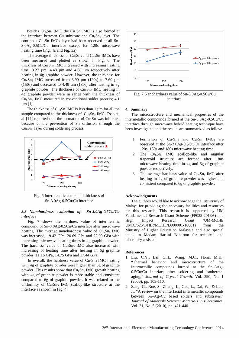
Fig. 7 Nanohardness value of Sn-3.0Ag-0.5Cu/Cu interface.
Besides Cu6Sn5 IMC, the Cu3Sn IMC is also formed at the interface between Cu substrate and Cu6Sn5 layer. The continous Cu3Sn IMCs layer had been observed at all Sn-3.0Ag-0.5Cu/Cu interface except for 120s microwave heating time (Fig. 4a and Fig. 5a). The average thickness of Cu6Sn5 and Cu3Sn IMCs have been measured and plotted as shown in Fig. 6. The thickness of Cu6Sn5 IMC increased with increasing heating time, 3.27 µm, 4.48 µm and 4.68 µm respectively after heating in 4g graphite powder. However, the thickness for Cu6Sn5 IMC increased from 3.90 µm (120s) to 7.60 µm (150s) and decreased to 4.49 µm (180s) after heating in 6g graphite powder. The thickness of Cu6Sn5 IMC heating in 4g graphite powder were in range with the thickness of Cu6Sn5 IMC measured in conventional solder process; 4.1 µm [1]. The thickness of Cu3Sn IMC is less than 1 µm for all the sample compared to the thickness of Cu6Sn5 IMC. Tsao et. al [14] reported that the formation of Cu3Sn was inhibited because of the prevention of Sn diffusion through the Cu6Sn5 layer during soldering process. 3.3 Nanohardness evaluation of Sn-3.0Ag-0.5Cu/Cu interface Fig. 7 shows the hardness value of intermetallic compound of Sn-3.0Ag-0.5Cu/Cu interface after microwave heating. The average nanohardness value of Cu6Sn5 IMC was increased; 19.42 GPa, 20.69 GPa and 22.09 GPa with increasing microwave heating times in 4g graphite powder. The hardness value of Cu6Sn5 IMC also increased with increasing of heating time after heating in 6g graphite powder; 11.16 GPa, 14.75 GPa and 17.44 GPa. In overall, the hardness value of Cu6Sn5 IMC heating with 4g of graphite powder were higher than 6g of graphite powder. This results show that Cu6Sn5 IMC growth heating with 4g of graphite powder is more stable and consistent compared to 6g of graphite powder. It was related to the uniformity of Cu6Sn5 IMC scallop-like structure at the interface as shown in Fig. 4.
4. Summary
The microstructure and mechanical properties of the intermetallic compounds formed at the Sn-3.0Ag-0.5Cu/Cu interface through microwave hybrid heating technique have been investigated and the results are summarized as follow:
1. Formation of Cu6Sn5 and Cu3Sn IMCs are
observed at the Sn-3.0Ag-0.5Cu/Cu interface after 120s, 150s and 180s microwave heating time.
2. The Cu6Sn5 IMC scallop-like and angular trapezoid structure are formed after 180s microwave heating time in 4g and 6g of graphite powder respectively.
3. The average hardness value of Cu6Sn5 IMC after heating in 4g of graphite powder was higher and consistent compared to 6g of graphite powder.
Acknowledgments The authors would like to acknowledge the University of
Malaya for providing the necessary facilities and resources for this research. This research is supported by UM Fundamental Research Grant Scheme (FP025-2013A) and High Impact Research Grant (UM-MOHE UM.C/625/1/HIR/MOHE/D000001-16001) from the Ministry of Higher Education Malaysia and also special thank to Madam Hartini Baharom for technical and laboratory assisted.
“Thermal behavior and microstructure of the intermetallic compounds formed at the Sn–3Ag–0.5Cu/Cu interface after soldering and isothermal aging,” Journal of Crystal Growth. Vol. 290, No. 1 (2006), pp. 103-110.
2. Zeng, G., Xue, S., Zhang, L., Gao, L., Dai, W., & Luo, J., “A review on the interfacial intermetallic compounds between Sn–Ag–Cu based solders and substrates.” Journal of Materials Science: Materials in Electronics, Vol. 21, No. 5 (2010), pp. 421-440.
Fig. 6 Intermetallic compound thickness of Sn-3.0Ag-0.5Cu/Cu interface
Conventional solder process [1]
36th International Electronic Manufacturing Technology Conference, 2014
3. Kim, K. S., Huh, S. H., & Suganuma, K., “Effects of intermetallic compounds on properties of Sn–Ag–Cu lead-free soldered joints,” Journal of Alloys and Compounds, Vol. 352, No. 1-2 (2003), pp. 226-236.
4. Wu, C. M. L., Yu, D. Q., Law, C. M. T., & Wang, L., “Properties of lead-free solder alloys with rare earth element additions.” Materials Science and Engineering: R: Reports, Vol. 44, No. 1 (2004), pp. 1-44.
5. Abtew, M., & Selvaduray, G., “Lead-free Solders in Microelectronics”. Materials Science and Engineering: R: Reports, Vol. 27, No. 5-6 (2000), pp. 95-141.
6. Moon, K.-S., Li, Y., Xu, J., & Wong, C. P., “Lead-free interconnect technique by using variable frequency microwave,” Journal of Electronic Materials, Vol. 34, No. 7 (2005), pp. 1081-1088.
7. Tasnim Firdaus Ariff, Brian Gabbitas and Deliang Zhang, “The effect of powder sintering method on the densification and microstructure of pewter alloys”. Materials Science and Engineering,Vol. 4 (2009), pp 1-5.
8. Roy, R., Agrawal, D., Cheng, J., Gedevanishvili, S. “Full sintering of powdered-metal bodies in a microwave fiel,” Nature, Vol. 399, (1999), pp. 668-670.
9. Srinath, M. S., Sharma, A. K., & Kumar, P., “A new approach to joining of bulk copper using microwave energy”. Materials & Design, Vol. 32, No. 5 (2011), pp 2685–2694.
10. Anklekar, R. M., Agrawal, D. K., & Roy, R., “Microwave sintering and mechanical properties of PM copper steel,” Powder Metallurgy,. Vol. 44, No. 4 (2001), pp. 355–362.
11. Zhao, C., Vleugels, J., Groffils, C., Luypaert, P.J. “Hybrid sintering with a tubular susceptor in a cylindrical single-mode microwave furnace,” Acta Materilia, Vol. 48, (2000), pp. 3795-3801.
12. Fallahi, H., Nurulakmar, M.S., Fallahi, A., Jamaluddin Abdullah, “Modifying the mechanical properties of lead-free solder by adding iron and indium and using a lap joint test,” Journal of Materials Science: Materials in Electronics. Vol. 23, No. 9 (2012), pp. 1739-1749.
13. Laurila, T., Vourinen, V., Kivilahti, J.K., “Interfacial reactions between lead-free solders and common base materials,” Materials Science and Engineering R, Vol. 45 (2005), pp 1-60.
14. Tsao, L.C., Chu, C.P., Peng, S.F., “Study of interfacial reaction between Sn3.5Ag0.5Cu composite alloys and Cu substrate,” Microelectronic Engineering, Vol. 88, (2011), pp. 2964-2969.