66 Effective Decap Insertion in Area-Array SoC Floorplan Design CHAO-HUNG LU National Central University, Taoyuan, Taiwan HUNG-MING CHEN National Chiao Tung University, Hsinchu, Taiwan and CHIEN-NAN JIMMY LIU National Central University, Taoyuan, Taiwan As VLSI technology enters the nanometer era, supply voltages continue to drop due to the reduction of power dissipation, but it makes power integrity problems even worse. Employing decoupling capacitances (decaps) in floorplan stage is a common approach to alleviating supply noise problems. Previous researches overestimate the decap budget and do not fully utilize the empty space of the floorplan. A floorplan usually has a lot of available space that can be used to insert the decap without increasing the floorplan area. Therefore, the goal of this work is to develop a better model to calculate the required decap to solve the power supply noise problem in area-array based designs, and increase the usage of available space in the floorplan to reduce the area overhead caused by decap insertion. The experimental results of this work are encouraging. Compared with previous approaches, our methodology reduces 38% of the decap budget in average for MCNC benchmarks but can still meet the power supply noise requirements. The final floorplan areas with decap are also smaller than the numbers reported in previous works. Categories and Subject Descriptors: J.6 [Computer-Aided Engineering]—Computer-aided de- sign (CAD) General Terms: Algorithm, Reliability Additional Key Words and Phrases: Power supply noise, floorplan, decap insertion ACM Reference Format: Lu, C.-H., Chen, H.-M., and Liu, C.-N. J. 2008. Effective decap insertion in area-array SoC floor- plan design. ACM Trans. Des. Automat. Elect. Syst. 13, 4, Article 66 (September 2008), 20 pages, DOI = 10.1145/1391962.1391974 http://doi.acm.org/10.1145/1391962.1391974 This work was supported in part by the National Science Council under contract NSC 96-2220-E- 009-013 and NSC 97-2220-E-009-001. Authors’ addresses: C.-H. Lu and C.-N. J. Liu, Department of Electrical Engineering, National Central University, Taoyuan, 320 Taiwan; email: {chiu, jimmy}@ee.ncu.edu.tw; H.-M. Chen, Department of Electronics Engineering and SoC Research Center, National Chiao Tung University, Hsinchu, 300 Taiwan; email: [email protected]. Permission to make digital or hard copies of part or all of this work for personal or classroom use is granted without fee provided that copies are not made or distributed for profit or direct commercial advantage and that copies show this notice on the first page or initial screen of a display along with the full citation. Copyrights for components of this work owned by others than ACM must be honored. Abstracting with credit is permitted. To copy otherwise, to republish, to post on servers, to redistribute to lists, or to use any component of this work in other works requires prior specific permission and/or a fee. Permissions may be requested from Publications Dept., ACM, Inc., 2 Penn Plaza, Suite 701, New York, NY 10121-0701 USA, fax +1 (212) 869-0481, or [email protected]. C 2008 ACM 1084-4309/2008/09-ART66 $5.00 DOI 10.1145/1391962.1391974 http://doi.acm.org/ 10.1145/1391962.1391974 ACM Transactions on Design Automation of Electronic Systems, Vol. 13, No. 4, Article 66, Pub. date: Sept. 2008.
Transcript
66
Effective Decap Insertion in Area-Array SoCFloorplan Design
CHAO-HUNG LU
National Central University, Taoyuan, Taiwan
HUNG-MING CHEN
National Chiao Tung University, Hsinchu, Taiwan
andCHIEN-NAN JIMMY LIU
National Central University, Taoyuan, Taiwan
As VLSI technology enters the nanometer era, supply voltages continue to drop due to the reductionof power dissipation, but it makes power integrity problems even worse. Employing decouplingcapacitances (decaps) in floorplan stage is a common approach to alleviating supply noise problems.Previous researches overestimate the decap budget and do not fully utilize the empty space of thefloorplan. A floorplan usually has a lot of available space that can be used to insert the decapwithout increasing the floorplan area. Therefore, the goal of this work is to develop a better modelto calculate the required decap to solve the power supply noise problem in area-array based designs,and increase the usage of available space in the floorplan to reduce the area overhead caused bydecap insertion. The experimental results of this work are encouraging. Compared with previousapproaches, our methodology reduces 38% of the decap budget in average for MCNC benchmarksbut can still meet the power supply noise requirements. The final floorplan areas with decap arealso smaller than the numbers reported in previous works.
Categories and Subject Descriptors: J.6 [Computer-Aided Engineering]—Computer-aided de-sign (CAD)
General Terms: Algorithm, Reliability
Additional Key Words and Phrases: Power supply noise, floorplan, decap insertion
ACM Transactions on Design Automation of Electronic Systems, Vol. 13, No. 4, Article 66, Pub. date: Sept. 2008.
66:2 • C.-H. Lu et al.
1. INTRODUCTION
As Very Large Scale Integration (VLSI) technology enters the nanometer era,supply voltages continue to drop. This condition helps reduce power dissipation,but also decreases the noise margin of devices. Noise margin interference cansometimes generate erroneous chip functions, seriously reducing chip perfor-mance. As a result, the integrity problem has become one of the major factorsaffecting chip yield. Basically, the integrity issues can be categorized into sig-nal integrity problems and power integrity problems. This article focuses onthe power integrity problem caused by power supply noises such as the IR-dropand �I (delta-I, Ldi/dt) noise.
Many researchers have proposed various approaches to solving this problemin every design stage. The power/ground (P/G) network [Mitsuhashi and Kuh1992; Tan and Shi 2001; Su et al. 2002; Singh and Sapatnekar 2005; Fu et al.2005; Kahng et al. 2006] is an important factor in the supply noise problem.Power supply noise can be greatly improved by a better P/G network with min-imal penalty cost. Besides sizing the power lines [Dutta and Marek-Sadowska1989; Yan et al. 2004], employing decoupling capacitances (decaps) is a commonapproach to reducing supply noise. Traditionally, the decap insertion process isperformed after routing in the physical design flow. This method would wastemany unnecessary area of the decap budget to improve the noise and decreasethe efficiency of the decap budget. Therefore, more and more researchers pro-pose to insert the decap before routing. Yeh and Marek-Sadowska [2005] pro-posed a two-step decap insertion method to improve power supply noise in theplacement level. This method includes one prediction method and one correc-tion method. The prediction step estimates the required decap pessimistically.Although the decap size can be adjusted in the correction step, a smaller areaoverhead can be achieved if decap insertion can be considered at an earlierstage. Yan et al. [2005] and Zhao et al. [2002], proposed decap insertion meth-ods at the floorplan level to reduce supply noise. Unfortunately, these previousresearchers often overestimate the decap budget. They assume that the decapis able to fully supply the maximum current of the module, which is too pes-simistic in our observation. Besides the decap budget computation, previousworks do not fully use the available floorplan space. A floorplan usually has alot of available spaces that can be used to insert the decap without increasingthe floorplan area.
To make a high-performance and high pin-count IC, the area-array archi-tecture is often used. In this architecture, the signal bumps are uniformly dis-tributed over the chip. Therefore, the resistance from the core I/O to the signalbumps can be greatly reduced and larger number of I/Os can be accommo-dated. Chen et al. [2005] used this architecture in floorplanning to improve thepower supply noise. Because the area-array architecture has such advantages,more and more chips adopt this architecture to improve the power supply noiseand limited pin number problem. However, without decap insertion, the result-ing floorplans and the area-array architecture still suffer from supply noiseviolations.
The purpose of this work is to develop a better model for calculating the decaprequired to solve the power supply noise problem and to wisely use the available
ACM Transactions on Design Automation of Electronic Systems, Vol. 13, No. 4, Article 66, Pub. date: Sept. 2008.
Effective Decap Insertion in Area-Array SoC Floorplan Design • 66:3
Fig. 1. Using a two-step approach that includes a Power Supply Noise (PSN) driven floorplan-ning algorithm and a decap insertion algorithm to improve the power supply noise before routinglevel. (A) The flow chart of our methodology. (B) In the floorplan step, high current modules arenot abutted and we use minimal extensive area to insert the decap budget in decap insertionstep.
space in the floorplan to reduce the area overhead caused by decap insertion.Based on the area-array architecture, this article proposes a two-step approachthat includes a noise-driven floorplanning algorithm and a decap insertion ap-proach to suppressing power supply noise at the floorplan level, as Figure 1illustrates. First, we use a noise-driven floorplan algorithm to reduce the pos-sible noise. This article adopts a stronger adjacent module relation O-tree rep-resentation as the engine for supply noise driven floorplanning, and success-fully modifies the primary operations Delete and Insert in proposed framework.Second, we use a Noise-driven Decap Planning with Minimum Area Insertion(NDP MAI) approach to inserting minimal decaps into a noise-guided resul-tant floorplan, with blocks and decaps legalization. Note that this approachcan compute the approximative decap size for a real design, and then providethe optimal location for each deacp in floorplanning. After routing, we can usethe method in Kahng et al. [2006] to rectify our result, further improving thepower supply noise problem.
ACM Transactions on Design Automation of Electronic Systems, Vol. 13, No. 4, Article 66, Pub. date: Sept. 2008.
66:4 • C.-H. Lu et al.
Fig. 2. The example of Ldi/dt noise effect. A complete circuit is composed of two subcircuits, Aand B, as in (A). If the start time of switching activity for A and B is not the same, that is, ta �= tb,the voltage can remain at a high level, as in (B). If not, the unstable voltage increases for a shortperiod and the voltage drops below the high VDD constraint, as in (C).
The rest of this article is organized as follows: Section 2 describes the floor-plan design with power supply noise consideration, the new noise estima-tion method, decap budget computation, and problem formulation. Section 3presents the floorplanning algorithm and decap insertion approach for powersupply noise avoidance. Section 4 shows experimental results, and Section 5presents conclusions.
2. POWER DELIVERY AND SIGNAL INTEGRITY ISSUESIN AREA-ARRAY DESIGNS
As VLSI technology enters the deep submicron (DSM) era, chips contain morefunctions and are expected to have much better performance. At the same time,reduced supply voltages in modern chip design is tightening the noise margin.IR-drop and Ldi/dt (delta-I) noise are the main contributors in the noise marginissue, and this study focuses primarily on these sources of noise.
IR-drop is the unavoidable waste of electric charge when the circuit obtainsenergy from a power. However, as we move into DSM regime, the resistance ofthe connection wire affects the power consumption of the chip. The Ldi/dt noiseis also called SSN (simultaneous switching noise) or �I (delta-I) noise. Figure 2shows that Ldi/dt noise is a voltage fluctuation phenomenon. When multiplecircuits switch simultaneously, the circuit requires a lot of electric charges in onemoment. If the VDD pin cannot supply enough energy at that time, the voltagefluctuation margin might exceed the lower boundary constraint. Using VDDpins and the decap to enhance the stabilization of the power supply are popularmethods. This section describes our power delivery model, noise estimationmodel, and decap computation used in this article, and formulate our targetproblem.
2.1 Area-Array Power Delivery Model and Noise Estimation
In this article, the power source distribution is based on the area-array architec-ture. The area-array architecture is a mesh structure, and the VDD and GNDbumps are uniformly distributed across the die with signal bumps in fixed in-terspersed location, as illustrated in Figure 3(A). The resistance from the I/O tothe connection block is substantially decreased, therefore improves the perfor-mance of the power delivery. As a result, many high-performance chips adoptthe area-array architecture.
ACM Transactions on Design Automation of Electronic Systems, Vol. 13, No. 4, Article 66, Pub. date: Sept. 2008.
Effective Decap Insertion in Area-Array SoC Floorplan Design • 66:5
Fig. 3. Area-Array power delivery illustration. (A) Area-array footprint SoC. The VDD and GNDbumps are uniformly distributed across the die with signal bumps in fixed interspersed locations.(B) One module gets power from only four VDD pins and others VDD pins are ignored. (C) Thecurrent path from one VDD pin to module A.
In the area-array architecture, a VDD bump supplies the current to all mod-ules according to the direct proportion of the distance from the bump to themodule. Four neighboring VDD bumps (right-top, right-down, left-top and left-down) of the module supply the main current, as Figure 3(B) shows, so we com-pute the noise from these VDD bumps only. Since there exist many paths forcurrent delivery to the target module, we only consider the shortest and secondshortest paths for noise computation simplification. The main reason is thatcurrents follow the least-impedance paths when flowing from the VDD to thetarget module. Compared with this method with SPICE simulation, the erroris within 10%, which is proved by Zhao et al. [2002]. This computation methodis fast and the error can be controlled within tolerable range, so we use thismethod to compute the power supply noise in the floorplan level. Kirchhoff ’svoltage law can be used represent the noise calculation of each module:
V (k)noise =
∑Pj εT k
i j RPjk + LPjk
di j
dt, (1)
where V (k)noise denotes the power supply noise at module k, Pj denotes the path
from the power bump to node j , Pj k denotes the path from node j to node k, T k
denotes the union of shortest paths and the second shortest paths, RPj k denotesthe resistance of Pj k , LPj k denotes the inductance of Pj k and i j is the currentflowing along path Pj .
2.2 Decap Budgeting in Area-Array Architecture
Zhao et al. [2002] and Yan et al. [2005] assumed that the decap should fullysupply the maximum current of the module, as shown in the white region in
ACM Transactions on Design Automation of Electronic Systems, Vol. 13, No. 4, Article 66, Pub. date: Sept. 2008.
66:6 • C.-H. Lu et al.
Fig. 4. (A) The current consumption profile of module k. Ikgen is supplied by VDD pins only, and
Ikmax is supplied by VDD pins and the decap budget. (B) We use HSPICE to verify our method and
the approach used in Zhao et al. [2002], the simulation circuit is shown in Figure 2(A). We useinverters in Module A and Module B. In the simulation result, our method yields less requireddecap than Zhao et al. [2002].
Figure 4(A). In this environment, the decap budget is possibly over-estimated.Actually, the VDD pin continuously provides current when the chip is operating,as the grey region in Figure 4(A). Therefore, the required decap size can besignificantly reduced.
The required decap size can be obtained by the difference between the maxi-mum current (Imax) and the target current limit (Igen) for each module. Assumethe target current limit of module k is defined as Ik
gen, k = 1, 2, . . . , M , and themaximum switching current of module k is Ik
max . Let Ck be the required decapfor circuit k and Qk be the amount of electric charge for the Ck . Qk can thenbe obtained by the following equation based on the triangle model shown inFigure 4.
Qk =∫ tw1
tw0
Ikmax(t) dt −
∫ tw1
tw0
Ikgen(t) dt, (2)
where tw0 is the start time and tw1 is the finish time when the target moduleis in operational mode. The charge can be converted to the silicon area of thecapacitance fabrication as follows:
Ck = Qk
Vcon(3)
Skdecap = Ck
Cox(4)
where Vcon is the noise constraint of the voltage, Ck is the decap budget andSk
decap is the silicon area of Ck . Cox is the unit area capacitance of a MOS capac-itor and Cox = εox/tox , where εox is the permittivity of SiO2 and tox is the oxidethickness. We use SPICE to verify the accuracy of (2), and compare the resultwith Zhao et al. [2002]. In the experiment, we use 0.25 μm technology to dothis simulation. The supply voltage is set at 2.5V and the power supply noisetolerance level is set at 0.04V. tw0 is set at 0 ns and tw1 is set at 24 ns. Adopting
ACM Transactions on Design Automation of Electronic Systems, Vol. 13, No. 4, Article 66, Pub. date: Sept. 2008.
Effective Decap Insertion in Area-Array SoC Floorplan Design • 66:7
the Zhao et al. [2002] method to compute the required decap produces the re-sult of 112 pF. The decap budget is 96 pF when using (2). Figure 4(B) shows thesimulation result. The proposed method yields less required decap than Zhaoet al. [2002].
2.3 Problem Formulation
The goal of this article is to use minimum decap to solve the power supply noiseproblem in the floorplan level. In other words, we suppress power noise by eachmodule in different locations and empty minimal decap area to avoid possiblepower noise during floorplanning. The problem can be formulated as follows:
Given a set of modules, B1, B2, ..., Bm, current consumption, Ikgen and Ik
max, ofeach block Bk , 1 ≤ k ≤ m, a set of power bumps, P1, P2, ..., Pm, and the noiseconstraint for each module V k
con, find a feasible solution such that each moduleBk obtains an appropriate and minimal decap budget size DBSk, and minimumpenalty area when DBSk is inserted. At the same time, the voltage noise of moduleV (k)
noise must be smaller than the noise constraint V (k)con.
3. MINIMAL DECAP ALLOCATION IN POWER SUPPLY NOISEAWARE FLOORPLANNING
To solve the power supply noise problem, this article develops a two-stepmethodology to suppress and reduce noise at the floorplan level, as Figure 1illustrates. Since placing two high current consumption modules close togetherseriously increases noise, we first propose a noise-driven floorplan algorithm toimprove this issue; the idea is to place the high-current consumption modulesintelligently. The goal of our floorplan averages the high power consumptionblock at one chip. This method can bring two benefits: (1) the peak noise can beimproved; (2) the decap budget can be averagely planned at one chip. The emptyroom after floorplanning is small and dispersive. If many decaps are insertedinto one particular region, the area of the floorplan may increase because theempty room does not have enough space for the decap. We then propose a Noise-driven Decap Planning with Minimum Area Insertion (NDP MAI) approachto reducing the power supply noise and area overhead after floorplanning. Webriefly introduce the representation of O-tree and new needed operations, Deleteand Insert, and then discuss the feasible region of the decap budget. Finally,we discusse the compensation of the decap budget due to the resistance of thepower line.
3.1 O-Tree Based Power Supply Noise Aware Floorplanning
To obtain a better result for noise-driven floorplan, a suitable and controllablefloorplan representation is needed. Table I compares six floorplan representa-tions. We choose O-tree to be our representation, the main reason is that theadjacent relations can be directly obtained. High current consumption modulescan be placed at a distance from each other.
The O-tree is composed of a horizontal tree and a vertical tree, as shown inFigures 5(B) and 5(D). The horizontal (vertical) tree uses T (α, β) to representthe data structure, as shown in Figures 5(C) and 5(E), where T denotes the tree
ACM Transactions on Design Automation of Electronic Systems, Vol. 13, No. 4, Article 66, Pub. date: Sept. 2008.
66:8 • C.-H. Lu et al.
Table I. Six Floorplan Representations Comparison
Floorplan Adjacent Solution OperationRepresentation Relation Space [Wen and Yan 2002] Delete Insert
SP [Murata et al. 1995] Not Good O((m!)2) - -B*-tree [Chang et al. 2000] Good O(m!22m−2/m1.5) O(1) O(m)O-tree [Guo et al. 1999] Best O(m!22m−2/m1.5) O(m) O(m)TCG [Lin and Chang 2001] Good O((m!)2) O(m2) O(m2)CBL [Hong et al. 2001] Good O(m!23.−3/m1.5) O(m) O(m)DBL [Yan et al. 2005] Good O(m!2m−1) O(m) O(m)
The O-tree structure records stronger adjacent relations for each module, while the memory cost of DBL isminimal.
Fig. 5. An O-tree example. (A) One floorplan result. (B) Vertical tree of (A). (C) Vertical treerepresentation. (D) Horizontal tree of (A). (E) Horizontal tree representation.
type, α denotes the paternity of the tree structure, and β denotes the permuta-tion of modules. If the module touches another module horizontally (vertically),such as modules H and L in Figure 5, it could be easily observed in the hori-zontal (vertical) representation. If we use other representations, the adjacentrelation of each module is more difficult to be found.
Figure 6(A) shows the original O-tree operations. If module J is deleted, theoriginal Delete operation generates a LD-packing floorplan. The result is thattwo high-current modules (I and K) are placed at an adjacent location. In somespecial regions, they consume more power than other regions, and must usemore decap to reduce power supply noise. A similar situation occurs for the In-sert operation because it only considers the area and the wire length in originaloperation conditions. In accordance with the previous description, the originalO-tree operations can not control the neighboring blocks. Therefore, new trans-formation operations are necessary. These operations help avoid placing thehigh current consumption modules at adjacent locations. We propose two newtransformation operations:
—Delete: The original operation deletes the selected module only. The new op-eration can delete the selected module and top-right modules of the selectedmodule.
—Insert: The original operation considers the area factor only. The module canbe inserted into a low noise location and an extensive area can be minimizedin our new operation.
ACM Transactions on Design Automation of Electronic Systems, Vol. 13, No. 4, Article 66, Pub. date: Sept. 2008.
Effective Decap Insertion in Area-Array SoC Floorplan Design • 66:9
Fig. 6. The difference between operations in the original O-tree and our approach. The plannedoperation is to delete and to insert module J. If we use the original operations to change thefloorplan in (A), high current consumption modules are possibly placed in the adjacent location.New operations can improve this problem, as (B), where high current consumption modules arenot placed together.
We use an example to explain new transformation operations. To delete mod-ule J in Figure 6(B), the selected module is module J and the top-right mod-ules of the selected module is module K only, so module J and module K mustbe deleted together. The reason that top-right modules must be deleted is be-cause the floorplan must maintain a LD-packing result. If the right-top modulesare not deleted at the same time, the high-current consumption module maybe placed at a neighboring location.
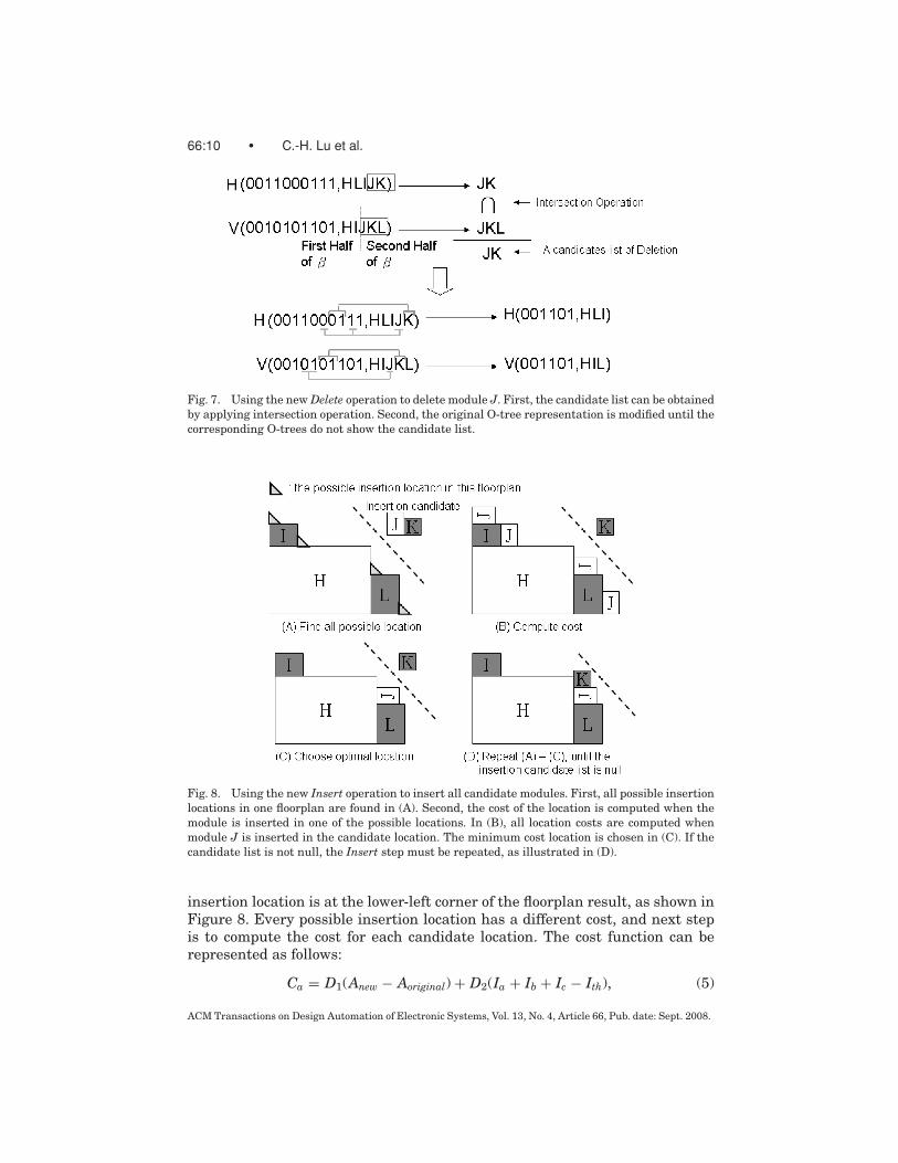
The new Delete operation consists of several steps. We first choose a to-be-deleted module ν from β of the horizontal and vertical O-trees, and then allmodules after ν in β are chosen. We could obtain two block sets φ and ϕ. We thenfind the intersection of φ and ϕ and obtain the candidate list of deletion modules.The final step in the Delete operation is to delete the modules at the intersectionof the vertical and horizontal O-tree. To clarify, we use an example to explain ourDelete operation. Figure 7 shows the horizontal and the vertical representationsof Figure 6. The horizontal representation is set as (0011000111,HLIJK) andthe vertical representation is set as (0010101101,HIJKL). In this case, moduleJ must be deleted. Therefore, the block set of φ includes modules J and K, andthe block set of ϕ includes modules J, K and L. The deletion candidate list,JK, can be obtained after the intersection: JK∩JKL. Finally, modules J andK in the representation are deleted. The horizontal representation changesto (001101,HLI), and the vertical representation is modified as (001101,HIL).The time complexity for the new Delete operation is O(m), where m denotes thenumber of modules.
The new Insert operation consists of three parts: (1) find all possible locations;(2) compute costs; (3) choose the optimal location. If one module is insertedin a floorplan, there are many locations to choose from, and the first step isto discover these candidate locations in a LD-packing floorplan. The possible
ACM Transactions on Design Automation of Electronic Systems, Vol. 13, No. 4, Article 66, Pub. date: Sept. 2008.
66:10 • C.-H. Lu et al.
Fig. 7. Using the new Delete operation to delete module J. First, the candidate list can be obtainedby applying intersection operation. Second, the original O-tree representation is modified until thecorresponding O-trees do not show the candidate list.
Fig. 8. Using the new Insert operation to insert all candidate modules. First, all possible insertionlocations in one floorplan are found in (A). Second, the cost of the location is computed when themodule is inserted in one of the possible locations. In (B), all location costs are computed whenmodule J is inserted in the candidate location. The minimum cost location is chosen in (C). If thecandidate list is not null, the Insert step must be repeated, as illustrated in (D).
insertion location is at the lower-left corner of the floorplan result, as shown inFigure 8. Every possible insertion location has a different cost, and next stepis to compute the cost for each candidate location. The cost function can berepresented as follows:
Ca = D1(Anew − Aoriginal) + D2(Ia + Ib + Ic − Ith), (5)
ACM Transactions on Design Automation of Electronic Systems, Vol. 13, No. 4, Article 66, Pub. date: Sept. 2008.
Effective Decap Insertion in Area-Array SoC Floorplan Design • 66:11
Fig. 9. The cost must compute twice for each corner because they are different during rotation.
where Ca denotes the cost when module A is inserted in this location, D1 and D2are the weights, Anew is the area of the floorplan after the module is inserted,Aoriginal is the original area, Ia(b,c) denotes the current consumption of the mod-ule a(b, c), and Ith denotes the threshold value for local current consumption.D2 is set at a large value for penalizing high local current consumption. Everycandidate location cost must be computed twice since costs are different whenthe insert module is directly inserted or rotated, as Figure 9 shows. Note thatEQ(5) considers the area and the power consumption only, this cost computa-tion can be extended by considering other objectives, such as wire length, etc.Finally, the module is inserted in the minimal cost location. The following illus-tration explains the new Insert operation. In Figure 8(A), the initial floorplanresult was made up of modules I, H and L and modules J and K are the insertmodule candidates. Four triangles denote the candidate location in the floor-plan. In Figure 8(B), we compute the cost after module J is inserted in all thecandidate locations. Finally, module J is inserted in the minimal cost location.In this case, the minimal cost location is at the corner between module H andmodule L, as Figure 8(C) shows. Because the candidate list is not null, the In-sert operation must be repeatedly applied, as shown in Figure 8(D). Note thatEQ(5) considers left and down adjacent modules only when calculating the costfunction. The main reasons for this are (1) Because the Insert operation mustmaintain a LD-packing floorplan, it only considers the left and down module ofA; (2) The Delete operation deletes all the top-right modules of A. If all modulesare inserted at the down-left corner only, there are no modules on the top andright side. The time complexity of the new Insert operation is O(m2), where mdenotes the number of modules.
According to previous operations and the SA (Simulated Annealing)[Kirkpatrick et al. 1983] algorithm, we propose a power-supply noise-drivenfloorplan algorithm, as illustrated in Figure 10. We first provide a floorplan re-sult and set the initial value for two annealing temperature parameters (line 2).The new Delete operation is used to delete modules (lines 4–6). Then, the newInsert operation and EQ(5) are used to insert modules (lines 7-11). After theInsert operation, the new LD-packing floorplan can be obtained. The difference(�C) between the new floorplan and the original floorplan is computed (line12). If �C is smaller than zero, it means that a better floorplan is obtained andwe would adopt this result to be our new solution (line 14). If not, we randomlydecide that the original floorplan must be replaced by the new floorplan (lines15–17). Finally, the temperature is cooled (lines 18).
ACM Transactions on Design Automation of Electronic Systems, Vol. 13, No. 4, Article 66, Pub. date: Sept. 2008.
66:12 • C.-H. Lu et al.
Fig. 10. The power-supply noise-driven floorplan algorithm.
3.2 Feasible Region for Decap Allocation
After obtaining one floorplan, we calculate the required decap size for eachmodule. According to Murata et al. [1995], Chang et al. [2000], Guo et al. [1999],Lin and Chang [2001], Hong et al. [2001], and Yan et al. [2005], the empty roomafter floorplanning is small and dispersive. If a bigger decap is inserted intoone floorplan, the area of the floorplan may increase because the unitary emptyroom does not have enough space for the decap. Besides the area factor, thecharge/discharge time of the capacitance must be considered. The charge timeis substantially reduced when several smaller decaps form the required decap.Our method cuts required decap into four smaller decaps to minimally increasethe floorplan area and reduce the charge/discharge time of the decap. Notethat the sizes of each smaller decap are not the same. The distribution is basedon the Manhattan distance from the VDD source to the power bump and (Px , Dx)denotes the connection relation. Px denotes the Manhattan distance from themodule’s VDD location to the power bump x and Dx denotes the obtainablecurrent contribution ratio from the power bump x. The computational equationof the current contribution ratio can be written as follows:
Dx =1
Pa,(a �=x)+ 1
Pb,(b�=x,a)+ 1
Pc,(c �=x,a,b)
Px + 1Pa,(a �=x)
+ 1Pb,(b�=x,a)
+ 1Pc,(c �=x,a,b)
, (6)
where (a �= x) denotes a and x are the different power bump. Pa,(a �=x) denotesthe power bump source of Pa and Px are different. In accordance with Eq. (6),
ACM Transactions on Design Automation of Electronic Systems, Vol. 13, No. 4, Article 66, Pub. date: Sept. 2008.
Effective Decap Insertion in Area-Array SoC Floorplan Design • 66:13
Fig. 11. The planned decap budget is partitioned into four smaller decaps. Each smaller decapis given a feasible region that ranges from the location of the power bump to the VDD source, asin (A). For each power bump, we set the supply current according to the distance from the powerbump to the VDD source, as in (B). Based on these constraints, a smaller decap can be insertedinto the chip and the charge time of the capacitance can be substantially decreased.
Dx is inversely proportional to Px , it is to follow the current divided theorem.A simple example helps to explain Eq. (6). Figure 11(A) shows a result of thefloorplan. Block D needs decap to supply the current consumption. We first useEqs. (2)–(4) to compute the optimal decap sizing. We then use Eq. (6) to computethe current ratio for each power bump, as Figure 11(B) shows.
In modern chip design, the decap is inserted in the empty space after detailedrouting. In reality, the decap can not improve the power noise for the high-current consumption module if the distance from the decap to the module isfar. To effectively utilize the energy for each decap, the rectangle scope fromthe power bump to the VDD pin is the feasible region for each small decap, asshown in Figure 11(A).
3.3 Identification of Space Priority for Decap Insertion
After floorplanning, the chip has some exploitable space for decap insertion. Ifthese spaces can be fully utilized, the cost of the chip might not increase evenwhen the decap is inserted into the chip. This section discusses the effect of plac-ing the decap in each different space. Furthermore, we propose a Noise-drivenDecap Planning with Minimum Area Insertion approach that simultaneouslyconsiders the area cost and the noise effect.
In a floorplan result, it certainly has one or more horizontal (vertical) longestpaths. The path notes the maximum width (height) of the floorplan. As shownin Figure 12, module H and L compose a horizontal longest path. Varying thesemodules directly modifies the area. Therefore, if one decap is inserted in thechannel space between these modules, the area would increase significantly.This channel space is called the extensive space. A channel space that over-laps edge of the empty room is called the empty space that is not held by anymodule. If one decap is inserted in this space, the location of each module doesnot change. The remaining channel spaces are called the available space exceptfor the channels of the extensive and empty space. If one decap is inserted inthis space, the area of the floorplan is fixed and the location of some modulesshifts only slightly. In Figure 12, the horizontal longest path is H → L andthe vertical longest path is H → I. If one decap is inserted into the extensive
ACM Transactions on Design Automation of Electronic Systems, Vol. 13, No. 4, Article 66, Pub. date: Sept. 2008.
66:14 • C.-H. Lu et al.
Fig. 12. When the decap is inserted into different spaces in a floorplan, the area of the floorplanmight increase. (A) The area of the floorplan is 2280 μm2 before the decap insertion. (B) The areaof the floorplan is 2565 μm2 after the decap insertion. The area does not increase when the decap isinserted into the empty space. If the decap is inserted into the available space, the area increasessometimes.
space between H and I, the area would increase 285 μm2. If one decap is in-serted into the empty space corner between H and I, the area and the topologyare not affected. Hence, the cost is lowest when the decap is inserted in theempty space. If the decap is inserted into the available space between L andJ, the area is not increased but the topology changes. Therefore three types ofspaces are the candidates location for the decap—Available Space, ExtensiveSpace and Empty Space. The priorities of these spaces are defined as follows:Empty Space > Available Space > Extensive Space. The minimum cost spacewill be selected for the decap insertion. Figure 13 illustrates the NDP MAIapproach.
3.4 Decap Compensation for Voltage Drop in Power Network
When using Eqs. (2)–(4) to calculate the required decap for each module, thedecap must be placed around the target. The NDP MAI approach does not con-sider this factor when placing the decap. If the location of the decap is notnear the target, the power supply noise violates the given constraint becausea part of the supply power from the decap would be consumed by wire resis-tance. To improve this problem, we use a simple compensative computation asfollows:
Qkcom = Qk + V (l × c) (7)
where Qkcom is the required decap of module k after the compensation, V is the
supply voltage, l is the distance from the space to the connection point, and c isthe wire capacitance per unit length. Although we could compensate the powerconsumption of the wire by Eq. (7), the power network is another importantissue that affects the supply power of the decap. Figure 14(A) shows the powernetwork after the decap insertion. We could utilize the superposition theoremto analyze the circuit, as Figures 14(B) and 14(C) shows. The discharge currentfrom the decap disperses to different modules because they both depend on thesame power network. If decap budget computations do not consider this factor,the power supply noise constraint may be violated.
ACM Transactions on Design Automation of Electronic Systems, Vol. 13, No. 4, Article 66, Pub. date: Sept. 2008.
Effective Decap Insertion in Area-Array SoC Floorplan Design • 66:15
Fig. 13. The NDP MAI flow chart. Using this approach, the module obtains sufficient energy anduses minimal extended area to finish the decap insertion.
To solve the above problem, we need a more accurate compensation equationfor Eq. (7). In accordance with the current divided theorem,
Qkcom = Qk × Rsk + Rsk
Rsk+ V (l × c), (8)
where Rsk is the total resistance on the side of the module k and Rsk is the totalresistance of other sides (Figure 14(B)). Equation (8) can accurately compensatethe required decap. We use SPICE to verify the accuracy of these two compen-sative equations. In our experiment (the circuit in Figure 14), these modules areof the same resistance. We expect module B to obtain 2.75 mA from decap. If weuse Eq. (7) to correct the decap, module B obtains only 2.66 mA, which is insuffi-cient for module B. If we use Eq. (8) to adjust the decap, it obtains 2.78 mA fromdecap. This experiment shows that the module can obtain sufficient current
ACM Transactions on Design Automation of Electronic Systems, Vol. 13, No. 4, Article 66, Pub. date: Sept. 2008.
66:16 • C.-H. Lu et al.
Fig. 14. Circuit analysis for the power network. (A) denotes the power network after the decapinsertion and it has two VDD sources. Using superposition theorem in (A), the decomposed resultsappear in (B) and (C).
from the decap when we use Eqs. (2)–(4) and Eq. (8) to compute the requireddecap.
4. EXPERIMENTAL RESULTS
This article implemented the Power-supply Noise-driven floorplan algorithm,the NDP MAI approach, and the approach in [Zhao et al. 2002] using C++language on an AMD 3200 computer with 1G memory. Tables II and IV comparethe run-time, peak noise, and decap budget with Zhao et al. [2002]. To obtainan equivalent comparison, the original cost function of Zhao et al. [2002] is“(A+ δA) + λ1(W + δW )”, where “λ1(W + δW )” denotes the wire length cost. Weset λ1 as zero because the wire length is not considered in our cost function.Five MCNC benchmark circuits, apte, hp, xerox, ami33 and ami49 are usedto test the performance of proposed methodology. Since the MCNC benchmarkincludes no noise constraint, the noise constraint is set at 0.13V and 0.25V.In our experiments, the operation times tw0 and tw1 of the switching currentwaveform are set to be 0.3 and 0.8. The power supply voltage is 1.2V and thedistance between two continuous VDDs is 1000�/μm and the power supplymesh is 333.3�/μm. We use Zhao et al. [2002]’s method to generate the current
ACM Transactions on Design Automation of Electronic Systems, Vol. 13, No. 4, Article 66, Pub. date: Sept. 2008.
Effective Decap Insertion in Area-Array SoC Floorplan Design • 66:17
Table II. Peak Noise after Floorplanning and the Decap Insertion
Our Method [Zhao et al. 2002]Peak Noise(V) Peak Noise Run Peak Noise(V) Peak Noise Run
Decaps obtained from our model and Zhao et al. [2002] are on the same resultant floorplan, and we useEq. (1) to compute the peak noise.
consumption information of each module: Ikgen denotes the target current limit
of module k, Ikgen = Ak × Dc, where Ak is the area of module k, and Dc is the
worst case current density; Ikmax denotes the maximum current of module k and
it is assigned as a random value to be 1.05Ikgen ∼ 2Ik
gen.Table II compares our method with Zhao et al. [2002], showing the peak noise
at noise-aware floorplanning (noise-driven) and the post-floorplanning decapinsertion (post). Experimental results show that our floorplan method obtainsbetter results than Zhao et al. [2002] does. The main reason for this is thatthe high current consumption modules are placed apart when we use Eq. (1) tocompute the peak noise. The time complexity of our floorplan method is slightlyhigher than the method in Zhao et al. [2002]. There are two reasons: (1) Thetime complexity of the original Insert operation is O(m) and the new Insert op-eration is O(m2). The time complexity of new operations is higher than originalO-tree operations; (2) Zhao et al. [2002] use the sequence pair-based floorplan-ner to plan blocks. The sequence pair method modifies the list order to changethe floorplan result. The time complexity for each change should be lower thanthe original O-tree method. In the post-floorplanning decap insertion, all resultsconform to the given constraint, 0.13V, and both run-times are very fast.
Table III clearly shows that our computation methodology obtains betterdecap budgets. For ami33 and ami49, the required decap budgets are reducedby 52% and 46%, respectively, and the noise conforms to the given constraint. Inaverage, this approach reduces the decap budget by 38%. The main reason forthis is that Zhao et al. [2002] ignores the supply current from VDD pins, and thetotal charge is supplied by the decap when the power supply noise occurs. Thistable also compares the peak noise. In all benchmarks, our peak noise is lower
ACM Transactions on Design Automation of Electronic Systems, Vol. 13, No. 4, Article 66, Pub. date: Sept. 2008.
66:18 • C.-H. Lu et al.
Table IV. Experimental Results for Some MCNC Benchmarks with Various Approaches forComparison
Zhao et al. [2002] Zhao et al. [2002]’s Decap Our MethodologyIncreased Area + Our Insertion Increased Area
The third column result and the fourth column result shows the advantage of our decap insertion method.The fourth column result and the fifth column result shows the advantage of our proposed framework(including floorplan, decap computation and insertion).
than the constraint level. On the other hand, we use the real circuit to verifythe accuracy of our experimental result. Simulations have been performed onami33 with HSPICE. The peak noise before decap insertion is 0.29V. If we useour proposed method, the peak noise is 0.11V. After applying Zhao et al. [2002]’smethod for decap insertion, the peak noise is 0.06V. These results are close toour results in Table III.
Table IV compares the area information of the proposed methodology withZhao et al. [2002]. In the third column, we completely use the Zhao et al. [2002]method to compute the increased area. In the fourth column, we partially adoptthe Zhao et al. [2002] method (including floorplan and decap computation) andour decap insertion method to obtain the increased area. The third columnand the fourth column show the advantage of our decap insertion method. Ourincreased area reduction comes from the fact that our method distributes com-puted decap into four smaller decaps to minimally increase the floorplan area.The incremental area of our proposed method is shown in the last column.Compared to the numbers reported in previous works, the proposed floorplan-ning framework creates better initial floorplans to work on, followed by theeffective NDP MAI approach to inserting enough decaps. In addition, we con-sider incorporating the proposed decap budgeting and insertion into the floor-planer, and compare that with our method. The experiment has been performedon ami49, in our method the peak-noise is 0.12V, the rum time is 12 seconds(shown in Table II) and the increased area is 154990 (μm2), but in integratedmethod the peak-noise is 0.10V, the rum time is increased to 921 seconds andthe increased area is 112652 (μm2). The results in both peak-noises conformthe constraint, and the integrated method can obtain better increased areareduction. Unfortunately, the penalty of the run time is very huge.
5. CONCLUSION AND FUTURE WORK
The techniques of floorplanning and decap insertion can be used to reduce powersupply noise in early design stages. The proposed framework can allocate a suit-able decap size. Furthermore, based on floorplan analysis and space priority,the decap insertion approach is proposed to insert the decap budget very ef-fectively. Experimental results show that the proposed method improves theincrease ratio of the floorplan area when inserting decaps.
ACM Transactions on Design Automation of Electronic Systems, Vol. 13, No. 4, Article 66, Pub. date: Sept. 2008.
Effective Decap Insertion in Area-Array SoC Floorplan Design • 66:19
In the modern chip design, the power gating technology [Hailin et al. 2005;Chiou et al. 2006] is frequently used to improve the leakage current. Therefore,a parallel process of the power gating and the decap will be explored to furtherimprove the decap budgeting and insertion approach.
ACKNOWLEDGMENTS
The authors would like to thank the anonymous reviewers for providing valu-able comments and suggestions that greatly improved this article.
REFERENCES
CHANG, Y.-C., CHANG, Y.-W., WU, G.-M., AND WU, S.-W. 2000. B*-trees: A new representation fornonslicing floorplans. In Proceedings of the IEEE/ACM Design Automation Conference. ACM,New York, 458–463.
CHEN, H.-M., HUANG, L.-D., LIU, I. M., AND WONG, D. 2005. Simultaneous power supply planningand noise avoidance in floorplan design. In IEEE Trans. Computer-Aided Des. Integr. Circ. Syst.578–587.
CHIOU, D., CHEN, S., CHANG, S., AND YEH, C. 2006. Timing driven power gating. In Proceedings ofthe IEEE/ACM Design Automation Conference. ACM, New York, 24–28.
DUTTA, R. AND MAREK-SADOWSKA, M. 1989. Automatic sizing of power/ground (P/G) networks inVLSI. In Proceedings of the IEEE/ACM Design Automation Conference. ACM, New York, 783–786.
FU, J., LUO, Z., HONG, X., CAI, Y., TAN, S. D., AND PAN, Z. 2005. VLSI on-chip power/ground networkoptimization considering decap leakage currents. In Proceedings of the IEEE Asia and SouthPacific Design Automation Conference. IEEE Computer Society Press, Los Alamitos, CA, 735–738.
GUO, P.-N., CHEN, C.-K., AND YOSHIMURA, T. 1999. An O-tree representation of nonslicing floorplanand its application. In Proceedings of the IEEE/ACM Design Automation Conference. ACM, NewYork, 268–273.
HAILIN, J., MAREK-SADOWSKA, M., AND SANI, R. 2005. Benefits and costs of power-gating tech-nique. In Proceedings of the IEEE International Conference on Computer Design. IEEE ComputerSociety Press, Los Alamitos, CA, 559–566.
HONG, X., HUANG, G., CAI, Y., GU, J., DONG, S., AND CHENG, C. 2001. Corner block list: An effectiveand efficient topological representation of non-slicing floorplan. In Proceedings of the IEEE/ACMDesign Automation Conference. ACM, New York, 764–769.
KAHNG, A. B., LIU, B., AND TAN, S. X.-D. 2006. Efficient decoupling capacitor planning via convexprogramming methods. In Proceedings of the International Symposium on Physical Design. 102–107.
KIRKPATRICK, S., GELATT, C., AND VECCHI, M. 1983. Optimization by simulated annealing. Science.671–680.
LIN, J.-M. AND CHANG, Y.-W. 2001. TCG: A transitive closure graph-based representation for gen-eral floorplans. In Proceedings of the IEEE/ACM Design Automation Conference. ACM, NewYork.
MITSUHASHI, T. AND KUH, E. 1992. Power and ground network topology optimization for cell basedVLSIs. In Proceedings of the IEEE/ACM Design Automation Conference. ACM, New York, 524–529.
MURATA, H., FUJIYOSHI, K., NAKATAKE, S., AND KAJITANI, Y. 1995. Rectangle-packing based mod-ule placement. In Proceedings of the IEEE/ACM International Conference on Computer-AidedDesign. ACM, New York, 472–479.
SINGH, J. AND SAPATNEKAR, S. 2005. Congestion-aware topology optimization of structuredpower/ground networks. IEEE Trans. Computer-Aided Des. Integr. Circ. Syst. 683–695.
SU, H., SAPATNEKAR, S., AND NASSIF, S. 2002. An algorithm for optimal decoupling capacitor siz-ing and placement for standard cell layouts. In Proceedings of the International Symposium onPhysical Design. 68–73.
ACM Transactions on Design Automation of Electronic Systems, Vol. 13, No. 4, Article 66, Pub. date: Sept. 2008.
66:20 • C.-H. Lu et al.
TAN, X. AND SHI, C. 2001. Fast power/ground network optimization based on equivalent circuitmodeling. In Proceedings of the IEEE/ACM Design Automation Conference. ACM, New York,550–554.
WEN, S.-J. AND YAN, J.-T. 2002. Double-bound list: A new placement representation with applica-tion to simulated-annealing-based floorplan. Unpublished.
YAN, J.-T., LIN, K.-P., AND CHEN, Y.-H. 2005. Decoupling capacitance allocation in noise-awarefloorplanning based on DBL representation. In Proceedings of the International Symposium onCircuits and Systems. 23–26.
YAN, J.-T., LU, C.-H., AND WU, C.-W. 2004. Simultaneous wiring and buffer block planning withoptimal wire-sizing for interconnect-driven floorplanning. In Proceedings of the IEEE MidwestSymposium on Circuits and Systems. IEEE Computer Society Press, Los Alamitos, CA, 25–28.
YEH, C. AND MAREK-SADOWSKA, M. 2005. Timing-aware power noise reduction in layout. In Pro-ceedings of the IEEE/ACM International Conference on Computer-Aided Design. ACM, New York,627–634.
ZHAO, S., ROY, K., AND KOH, C. 2002. Decoupling capacitance allocation and its application topower-supply noise-aware floorplan. IEEE Trans. Computer-Aided Des. Integr. Circ. Syst. 21,81–92.
Received May 2007; revised September 2007 and January 2008; accepted May 2008
ACM Transactions on Design Automation of Electronic Systems, Vol. 13, No. 4, Article 66, Pub. date: Sept. 2008.