Page 1
EFFECTS OF MOLYBDENUM NANOPARTICLES
ON THE INTERFACE BETWEEN LEAD-FREE
SOLDER AND NICKEL SUBSTRATE
MOHAMMAD HOSSEIN MAHDAVIFARD
RESEARCH PROJECT SUBMITTED IN PARTIAL
FULFILMENT OF THE REQUIREMENTS FOR THE
DEGREE OF MASTER OF ENGINEERING
FACULTY OF ENGINEERING
UNIVERSITY OF MALAYA
KUALA LUMPUR
2013
Page 2
ii
UNIVERSITY OF MALAYA
ORIGINAL LITERARY WORK DECLARATION
(I.C/Passport No: U19765890) Registration/Matric No:
Name of Candidate: Mohammad Hossein Mahdavifard
Name of Degree: MASTER OF MATERIALAS ENGINEERING AND TECH
Title of Project Paper/Research Report/Dissertation/Thesis (“this Work”):
Effect of Molybdenum nanoparticles on lead free solders on copper substrate with
Nickel layer
Field of Study: Materials Engineering
I do solemnly and sincerely declare that:
1) I am the sole author/writer of this Work;
2) This Work is original;
3) Any use of any work in which copyright exists was done by way of fair dealing
and for permitted purposes and any excerpt or extract from, or reference to or
reproduction of any copyright work has been disclosed expressly and
sufficiently and the title of the Work and its authorship have been
acknowledged in this Work;
4) I do not have any actual knowledge nor do I ought reasonably to know that the
making of this work constitutes an infringement of any copyright work;
5) I hereby assign all and every rights in the copyright to this Work to the
University of Malaya (“UM”), who henceforth shall be owner of the copyright
in this Work and that any reproduction or use in any form or by any means
whatsoever is prohibited without the written consent of UM having been first
had and obtained;
6) I am fully aware that if in the course of making this Work I have infringed any
copyright whether intentionally or otherwise, I may be subject to legal action or
any other action as may be determined by UM.
Candidate’s Signature Date
Subscribed and solemnly declared before,
Witness’s Signature Date
Name:
Designation:
Page 3
iii
Abstract
In this study, Mo nanoparticles were used as a reinforcing material into the Sn-3.8Ag-
0.7Cu (SAC) solder on the nickel substrate (Cu substrate with an electrodeposited Ni
layer on top). The Mo nanoparticles were characterized by transmission electron
microscopy (TEM) and X-ray diffractometer (XRD). The composite solder paste was
prepared by manually mixing Mo nanoparticles with the SAC solder paste. Nickel was
electrodeposited on polycrystalline copper substrate in the Watts bath. The solder paste
was placed on substrate at 250ºC for 45 seconds. After reflow, elemental compositions
of the nanocomposite solders were analyzed by inductively coupled plasma-optical
emission spectrometer (ICP-OES). The microstructural investigations, spreading rate
and wetting angle measurement were carried out on the solders after first reflow. After
that one set of samples were subjected to multiple reflow for up to six times.
Microstructural investigations were performed at the solder/substrate interface using high
resolution field emission scanning electron microscopy (FESEM) and energy dispersive X-
ray (EDX). Results reveal that after reflow only a fraction of Mo nanoparticles were
retained inside the solder matrix. The solder spreading rate was decreased and wetting
angle increased with the addition of Mo nanoparticles to the SAC solder. It was found
that Mo nanoparticles were effective in suppressing the growth of total IMC layer
thickness and scallop diameter during reflow. It was found that Mo nanoparticles did
not dissolve or react with the solder during reflow. The retardation of IMC thickness
was suggested to be due to the discrete particle effect of Mo nanoparticles. The intact,
discrete nanoparticles, by absorbing preferentially at the interface, hindered the
diffusion flux of the substrate and thereby suppressed the IMC growth. The retardation
of total IMC layer with the addition of Mo nanoparticles is expected to improve the
reliability of the solder joint.
Page 4
iv
Abstrak
Dalam kajian ini, nanopartikel Mo telah digunakan sebagai bahan pengukuh dalam Sn-
3.8Ag-0.7Cu (MPS) pateri pada substrat Nickel (substrat Cu dengan electrodeposited Ni
lapisan). Nanopartikel Mo telah disifatkan oleh penghantaran elektron mikroskop (TEM)
dan sinar-X diffractometer (XRD). Pes pateri komposit telah disediakan secara manual
dengan pencampuran nanopartikel Mo ke dalam pes pateri SAC. Nikel telah
electrodeposited pada polihabluran tembaga substrat dengan kaedah mandi watt. Pes
pateri diletakkan pada substrat apabila suhu mencapai 250 º C selama 45 saat. Selepas
reflow, komposisi unsur yang solders Komposit nano akan dianalisis oleh induktif yang
ditambah dengan spektrometer pelepasan plasma-optik (ICP-OES). Siasatan
mikrostruktur, kadar merebak dan sudut pembasahan telah dijalankan pada solders
selepas reflow pertama. Selepas itu, set sampel tersebut akan diuji dalam reflow selama
enam kali. Mikrostruktur siasatan akan dijalankan di antara permukaan pateri / substrat
dengan menggunakan bidang pelepasan imbasan mikroskop elektron (FESEM) yang
resolusi tinggi dan serakan tenaga sinar-X (EDX). Keputusan dari ujian menunjukkan
bahawa selepas reflow, hanya sebahagian kecil daripada nanopartikel Mo telah
mengekalkan dalam matriks pateri. Kadar menyebarkan telah menurun dan sudut
membasahkan meningkat dengan tambahan nanopartikel Mo dalam pateri MPS. Ia
didapati bahawa nanopartikel Mo berkesan dalam membenteras pertumbuhan jumlah
ketebalan lapisan IMC dan diameter kerang semasa reflow. Dengan tambahan
nanopartikel Mo, pekali penyebaran dikurangkan tetapi tenaga pengaktifan
pertumbuhan kerang IMC masih tidak berubah. Pembubaran substrat Cu dan
pembentukan IMC dikurangkan dengan kehadiran nanopartikel Mo.
Dari keputusan penyelidikan, ia telah mendapati bahawa nanopartikel Mo tidak larut
atau bertindak-balas dengan pateri semasa reflow. Ketebalan IMC dan diameter kerang
Page 5
v
terencat adalah disebabkan oleh kesan zarah diskret nanopartikel Mo. Tindak-balas,
nanopartikel diskret, dengan menyerap terutamanya pada permukaan, menghalang fluks
penyebaran substrat dan pertumbuhan IMC itu. Jumlah lapisan IMC yang terencat
dengan tambahan nanopartikel Mo meningkatkan kebolehpercayaan sendi pateri.
Page 6
vi
Acknowledgements
First, I would like to express my deep and sincere gratitude to my supervisor, Prof. Dr.
A.S. Md. Abdul Haseeb for his technical advices and constructive comments throughout
this dissertation.
I would like to sincere thanks to my dear friends and colleagues. Many thanks to Md.
Arafat Mahmood for his useful comments that improved the dissertation. Special thanks
to Hamid Taheri for being a very helpful friend.
Finally, the people close to my heart deserve the uppermost appreciation for their
support and patience. Many special thanks to my dear parents and my dear sister. I
always feel the warmth of their love.
Page 7
vii
Table of Contents
Abstract ........................................................................................................................... iii
Abstrak ............................................................................................................................ iv
Acknowledgements ......................................................................................................... vi
Table of Contents .......................................................................................................... vii
List of Figures .................................................................................................................. x
List of Notations ........................................................................................................... xiii
List of Abbreviation ..................................................................................................... xiv
Chapter 1: Introduction ................................................................................................. 1
1.1 Background .......................................................................................................... 1
1.2 Research Objectives ............................................................................................ 3
1.3 Scope of Research ............................................................................................... 4
1.4 Organization of Research Report ........................................................................ 5
Chapter 2: Literature Review ........................................................................................ 6
2.1 Soldering technology and theirs metallurgy ........................................................ 6
2.2 Key parameters of soldering ................................................................................ 8
2.2.1 Wetting and contact angle .......................................................................... 9
2.3 Health and Environmental Effects of Pb ........................................................... 10
2.4 Lead Free Solder Candidates ............................................................................. 11
2.4.1 Sn-Au ....................................................................................................... 13
2.4.2 Sn-Bi ........................................................................................................ 13
2.4.3 Sn-Zn........................................................................................................ 14
2.4.4 Sn-In ......................................................................................................... 14
2.4.5 Sn-Ag ....................................................................................................... 14
2.4.6 Sn-Cu ....................................................................................................... 14
2.4.7 Sn-Ag-Cu ................................................................................................. 15
2.5 Thermodynamics of Sn-Ag-Cu Solder Alloy Selection .................................... 15
2.6 Phase Diagram of Mo with Sn, Ag and Cu ....................................................... 18
2.7 Interfacial Reactions of Sn-Ag-Cu Solder with Substrate ................................. 19
2.7.1 Microstructure of Interfacial IMCs during reflow ................................... 20
Page 8
viii
2.8 Nucleation and Growth of Interfacial IMCs ...................................................... 26
2.8.1 Formation Mechanisms of Interfacial IMCs ............................................ 26
2.9 Effects of Alloying Elements on the Interfacial IMCs ...................................... 28
2.10 Effects of Nanoparticles on Interfacial IMC ................................................... 29
2.11 Electrodeposition of Nickel ............................................................................. 31
2.11.1 Average Coating Thickness ................................................................... 32
2.11.2 Functional Electroplating and Deposit Properties ................................. 33
2.12 Summary and Conclusion ................................................................................ 34
Chapter 3: Methodology ............................................................................................... 36
3.1 Raw Materials and Characterization.................................................................. 36
3.2 Sample Preparation and Treatment.................................................................... 36
3.2.1 Preparation of Copper Substrate with Electroplated Ni ........................... 36
3.2.2 Preparation of Composite Solder Paste and Nanoparticles Distribution . 37
3.2.3 Preparation of Reflowed Samples ............................................................ 38
3.2.4 Multiple Reflow ....................................................................................... 38
3.3 Characterization of Solder ................................................................................. 38
3.3.1 Differential Scanning Calorimetry Measurement of Solder Paste ........... 38
3.3.2 Inductively coupled-Optical Emission Spectrometer .............................. 39
3.3.3 Spreading Rate and Wetting Angle.......................................................... 39
Chapter 4: Results and Discussion .............................................................................. 41
4.1 Characterization of Raw Materials .................................................................... 41
4.1.1 Morphological Characterization and Particle Sizes of Solder Paste ........ 41
4.1.2 TEM of Mo Nanoparticles ....................................................................... 41
4.1.3 X-Ray Diffraction of Mo Nanoparticles .................................................. 42
4.2 Distribution of Mo Nanoparticles in the SAC Solder Paste .............................. 43
4.3 Chemical Analysis of the Reflowed Samples ................................................... 44
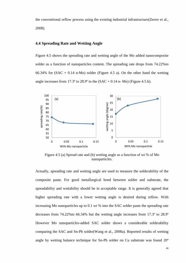
4.4 Spreading Rate and Wetting Angle ................................................................... 46
4.5 Analysis of Electroplated Ni on Copper Substrate ............................................ 47
4.6 IMC Morphology on Ni and Cu Substrate ........................................................ 48
4.7 Effect of Mo Nanoparticles on IMC .................................................................. 50
4.7.1 State of Mo Nanoparticles during Reflow ............................................... 52
4.7.2 Suggested Mechanism for Retardation of IMC Growth by Mo
Nanoparticles .................................................................................................... 52
Chapter 5: Conclusion and Recommendation ............................................................ 54
5.1 Conclusions ....................................................................................................... 54
Page 9
ix
5.2 Recommendation for Future Work .................................................................... 55
References ...................................................................................................................... 56
Page 10
x
List of Figures
Figure 2.1:a) Schematic illustration of the flip-chip joining process (Humpston and
Jacobson, 2004) b) Cross-section of a ball grid array (BGA) microelectronic
component (Abtew and Selvaduray, 2000). ..................................................... 8
Figure 2.2 surface tension forces acting when a liquid droplet wets a solid surface,
according to the classical model ...................................................................... 9
Figure 2.3 Phase diagram of the (a) Sn-Cu (Franke and Neuschütz, 2005), (b) Sn-Ag
(Karakaya and Thompson, 1987) and (c) Ag-Cu system (Xie and Zhang,
1998). ............................................................................................................. 16
Figure 2.4 Calculated liquidus surface of the Sn rich region of Sn-Ag-Cu alloy system
(Moon et al., 2000). ........................................................................................ 18
Figure 2.5Phase diagram of the (a) Mo-Sn (Brewer and Lamoreaux, 1980) b) Mo-Ag
(Baren, 1990) and (c) Mo-Cu (Baren, 1990).................................................. 19
Figure 2.6 IMC layers formed between the solder and Cu substrate after soldering
(Zhang et al., 2009). ....................................................................................... 21
Figure 2.7(a) The microstructure of IMC layer at the interface between solder and Cu
(Zhang et al., 2009). (b) SEM image of typical microstructure of Sn–Ag–Cu
solder I )Sn-rich, II) Cu6Sn5, and III) Ag3Sn (Pang et al., 2004a). ................ 22
Figure 2.8(a) Interface between Sn-3.0Ag-0.6Cu solder ball and Ni/Cu substrate (b)
Zoom-in view of (a) (Ho et al., 2007). ........................................................... 23
Figure 2.9 (a) Phase diagram for system Cu-Sn (Franke and Neuschütz, 2005) (b) Phase
diagram of Ni-Sn (Okamoto, 2006) (c) Partial phase diagram of the Cu-Ni-Sn
system at 235°C. It can be seen that the (Cu,Ni)6Sn5 compound extends to a
wide range of ternary compositions (Korhonen et al., 2000). ........................ 25
Figure 2.10 Formation mechanism of the fine Sn–Cu particles layer near the three-phase
contact line: a low temperature and b high temperature with the molten solder
ball (TZs transportation zones). ..................................................................... 27
Figure 4.1SEM image of SAC solder powder (Flux has been removed) (Arafat, 2012).
........................................................................................................................ 41
Figure 4.2 (a) TEM micrograph of the Mo Nano-particles, (b) Histogram of particle size
(Arafat, 2012). ................................................................................................ 42
Figure 4.3 X-Ray diffraction (XRD) patterns of Mo nanoparticles (Arafat, 2011). ....... 43
Page 11
xi
Figure 4.4FESEM images of solder paste after blending, nominally containing 2 wt% of
Mo nanoparticles (a) distribution of Mo nanoparticles into the solder paste, (b)
elemental mapping of the composite paste showing Mo (red), Sn (cyan), Ag
(blue), and Cu (yellow), (c) high resolution image focused on the solder ball
surface and (d) high resolution image focused on the flux (Arafat et al., 2011).
........................................................................................................................ 44
Figure 4.5 (a) Spread rate and (b) wetting angle as a function of wt % of Mo
nanoparticles. ................................................................................................. 46
Figure 4.6 SAC on copper substrate with a top layer of electroplated Ni. ..................... 47
Figure 4.7 IMC morphology of (a) SAC on Cu substrate after 1st reflow, (b) SAC+0.14
n-Mo on cu substrate after 1st reflow (c)SAC on Ni substrate after 1
st reflow
(d) SAC +0.14 n-Mo on Ni substrate after 1st reflow. ................................... 48
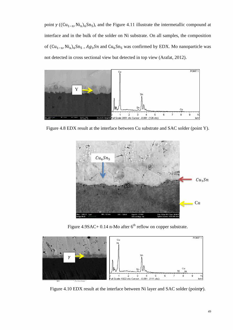
Figure 4.8 EDX result at the interface between Cu substrate and SAC solder (point Y).
........................................................................................................................ 49
Figure 4.9SAC+ 0.14 n-Mo after 6th
reflow on copper substrate. .................................. 49
Figure 4.10 EDX result at the interface between Ni layer and SAC solder (point ). .... 49
Figure 4.11 Intermetallic compound between the SAC solder and the Ni substrate. ..... 50
Figure 4.12Backscattered electron micrographs of the cross sectional view (a) SAC after
first times reflow, (b) (SAC + 0.04 n-Mo) after first times reflow, (c) (SAC +
0.14 n-Mo) after first times reflow ,(d) SAC after six times reflow and (e)
(SAC + 0.04 n-Mo) after six times reflow(f) (SAC + 0.14 n-Mo) after six
times reflow (All has same magnification of 4.00 KX). ................................ 51
Figure 4.13 Effect of Mo nanoparticles on the IMC thickness. ...................................... 51
Page 12
xii
List of Tables
Table 2.1 Binary Pb-free eutectic solders (Tu, 2010). .................................................... 11
Table 2.2 Nickel Electrodeposition Data (Mordechay Schlesinger, 2010) ..................... 33
Table 2.3 Nickel Plating Solutions (Mordechay Schlesinger, 2010). ............................. 34
Table 3.1 Plating solution and parameters for the deposition of Ni on Cu substrate
(Mordechay Schlesinger, 2010). .................................................................... 37
Table 3.2 Nickel electroplating data(Mordechay Schlesinger, 2010) ............................. 37
Table 4.1Molybdenum content of solders analyzed by ICP-OES after reflow............... 45
Page 13
xiii
List of Notations
SAC = Sn-3.8Ag-0.7Cu
Sn = Tin
Ag = Silver
Cu = Copper
Pb = Lead
Mo = Molybdenum
Co = Cobalt
Ni = Nickel
Au = Gold
Bi = Bismuth
Zn = Zinc
In = Indium
IMC = Intermetallic compound
H2SO4 = Sulphuric acid
HNO3 = Nitric acid
HCl = Hydrochloric acid
CNT = Carbon nanotube
TiO2 = Titanium dioxide
Al2O3 = Alumina
nm = Nanometer
= Micrometer
Page 14
xiv
List of Abbreviation
TEM = Transmission Electron Microscopy
SEM = Scanning Electron Microscopy
FESEM = Field Emission Scanning Electron Microscopy
EDX = Energy Dispersive X-Ray
XRD = X-ray Diffraction
DSC = Differential Scanning Calorimeter
ICP-OES = Inductive Couple Plasma- Optical Emission Spectrometer
ITRS = International Technology Roadmap for Semiconductor
EPA-US = Environmental Protective Agency-United States
NCMS = National Center for Manufacturing Science
EU = European Union
WEEE = Waste Electrical and Electronic Equipment
IC = Integrated Circuit
PCB = Printed Circuit Board
BGA = ball Grid Array
FC = Flip Chip
SMT = Surface Mount Technology
PIH = Pin in Hole
PTH = Pin through Hole
OSP=Organic Solderability Preservative
NEMI= National Electronics Manufacturing Initiative
RoHS= Restriction of hazardous substance Directives
Page 15
1
Chapter 1: Introduction
1.1 Background
Soldering is one of the important famous joining methods that use a filler metal with a
melting point below 425°C. In the immense electronic materials world, solder plays a
vital role in the assembly and interconnection of the silicon die (or chip). As a joining
material, solder provides electrical, thermal and mechanical continuity in electronics
assemblies. The performance and quality of the solder are crucial to the integrity of a
solder joint, which in turn is vital to the overall functioning of the assembly (Abtew and
Selvaduray, 2000).
The primary solder alloy design criteria have been developed by using Sn-Pb eutectic as
a baseline. For more than fifty years, printed wiring boards (PWB) and components had
been designed around the behavior of Sn-Pb eutectic solder during circuit board
assembly and in use for holding components to the PWBs (Bath, 2010). As a result of
toxicity of Pb, the new standard Pb-free alloy replaces Sn-Pb eutectic solder in a wide
variety of board designs and microelectronics applications.
The Waste Electrical and Electronic Equipment (WEEE) Directive encourages
increased recycling of electrical and electronic products. However, the recycling effort
is typically an end-of-use action that occurs just prior to potential disposal. As a purely
environmental strategy, Pb elimination/replacement appears to be a better approach,
unless the substitutions cause more problems than they solve (Ganesan and Pecht, 2006).
By 1999, the WEEE and Restriction of Hazardous Substance Directives (RoHS) led
National Electronics Manufacturing Initiative (NEMI) to establish a less quantitative,
but no less restrictive, set of criteria. The NEMI alloy was designed to:
1. Have a melting point as close as possible to Sn-Pb eutectic
Page 16
2
2. Be eutectic or very close to eutectic alloy
3. Contain maximum three elements (ternary composition)
4. Avoid using existing patents (avoid legal obligation)
5. Have the potential for reliability equal to or better than Sn-Pb eutectic solder
(Bath, 2010).
All research groups agreed that there were no “drop-in” replace ent alloys for Sn-Pb
eutectic. Applications of these criteria led the NEMI to choice the Sn-Ag-Cu ternary
system, more specifically the Sn-3.9Ag-0.6Cu (± 0.2%) alloy that it has the most
promising properties for surface mount application.
One of the major challenges in the development of a reliable Pb-free solder is to
improve the mechanical, interfacial properties and reliability of the solder joints (Koo
and Jung, 2005). The microstructure of SAC alloys has been found to coarsen to a
greater extent during use and during high temperature exposure as compared with that
of their Pb containing counterparts (Cheng et al., 2009). Moreover, Sn based solders
form thicker intermetallic compound (IMC) layer at the solder/substrate interface
compared with the Pb based solders (Wu et al., 2004). The interfacial IMCs in Pb-free
solder also grow at a faster rate than that in Pb-based solders. Coarsening of
microstructure and rapid growth of brittle interfacial IMC are known to degrade the
properties of lead free solder joints resulting in lower long term reliability.
Adding appropriate additions to Sn based solder is one approach to improve its
properties. Alloy addition (Wang et al., 2008b) and particle additions (Das et al., 2009,
Shen and Chan, 2009) has been studied recently. Adding particles to Sn based solder
results in the development of composite solders with superior properties. Addition of
diverse types and sizes of particles are under investigations. Many kinds of particles that
have been investigated until now include metallic (Amagai, 2008, Lin et al., 2002),
ceramics (Shen and Chan, 2009) and carbon nanotubes (Kumar, 2009) . Both
Page 17
3
micrometer (Das et al., 2009) and nanometer (Shi et al., 2008) sized particles are
currently being considered.
The reason behind particle addition is that by adding appropriate types of particles to the
solder, they should lead to dispersion strengthening. They are also anticipated to
stabilize the microstructure by limiting the growth of different phases in the solder
during use. Nanoparticles addition to tin based solders are attracted many consideration
in recent years (Amagai, 2008). With the miniaturization of solder pitch size in
electronic packages, the additions of nanoparticles are becoming more reliable method
to reach the criteria of proper solder joint.
Improving in bulk mechanical properties like strength (Shen and Chan, 2009), hardness
(Gain et al., 2011), creep resistance (Shi et al., 2008) etc. have been perceived in Pb-free
solders reinforced by nanoparticles additions. Specifically, the addition of Mo
nanoparticles has led in significant improvement in the bulk mechanical properties of
solder (Chandra Rao et al., 2010, Kumar et al., 2005). Nevertheless, the integrity of a
solder joint not only depends on its bulk properties, but also relies on the interfacial
properties of the solder/substrate. Therefore, it is important to investigate the effect of the
nanoparticles additions on the interfacial characteristics. Only a few studies are available on
the influence of nanoparticles on the interfacial IMC.
1.2 Research Objectives
The objectives of this research are listed below:
1. To examine the wetting and reflow characteristics of Sn-3.8Ag-0.7Cu solder on Ni
substrate with and without Mo nanoparticles.
2. To investigate the effects of Mo nanoparticles on the morphology and growth of
intermetallic compounds during reflow on Ni substrate
Page 18
4
3. To compare the effects of Ni substrate with Cu substrate in present of Mo
nanoparticle on the morphology and growth of intermetallic compounds during
reflow.
1.3 Scope of Research
The overall purpose of this research is to investigate the effect of molybdenum (Mo)
nanoparticles on the interfacial reactions between Sn-3.8Ag-0.7Cu solder and Ni
substrate, during multiple times of reflow. Therefore, Mo nanoparticles were manually
mixed with the SAC solder paste at various wt% to prepare composite solder paste. A
Ni layer was deposited on copper substrate and solder joints were prepared on the
substrate under standard experimental conditions.
The characterizations of nanocomposite solder joints were carried out using several
analytical methods. SAC solder joint was used as an experimental reference. All
obtained data were compared and analyzed with other published works. The
characterization of raw materials was carried out thoroughly by transmission electron
microscopy (TEM), field emission scanning electron microscopy (FESEM) and X-ray
diffraction (XRD) analysis. The melting behavior of the nanocomposite solders was
investigated by differential scanning calorimeter (DSC). Inductively coupled plasma-
optical emission spectrometry (ICP-OES) was utilized to find the actual amount of
nanoparticles incorporated to the solder. The spreading rate and wetting angle of the
solders were measured by the Japanese Industrial Standard (JIS Z3198-3, 2003). The
interfacial microstructure following the solder samples were investigated by optical
microscopy, conventional SEM, high resolution field emission SEM (FESEM) equipped
with Energy Dispersive X-Ray (EDX).
Page 19
5
1.4 Organization of Research Report
This research report consists of five chapters. Chapter 1 introduces briefly this research
work. This chapter consist of the research background, the current technical problems in
this field, research objectives and the scope of this research. Chapter 2 gives a general
overview of the previous research on various topics related with this research. It
includes electronic packaging and soldering technology, lead-free solder candidates,
thermodynamics of alloy selection, interfacial reaction between the solder and substrate
during reflow, Ni electroplating, effect of alloying elements and effects of nanoparticles
on the solder. In Chapter 3, the experimental procedure is explained which consist of the
procedures of sample preparations and electro-deposition, characterization techniques, the
equipment, fixtures and procedure used during characterization. Chapter 4 reports the
results from the experimental work and interpretation on the basis of analyze and
comparison with the previous published document. Chapter 5 includes a brief summary of
this research report and the recommendation for future work.
Page 20
6
Chapter 2: Literature Review
2.1 Soldering technology and theirs metallurgy
Soldering involve using a molten filler metal to wet the mating surfaces of a joint, with
or without the aid of a fluxing agent, leading to the formation of metallurgical bonds
between the filler and the respective components. In these processes, the original
surfaces of the co ponents are “eroded” by virtue of the reaction occurring between the
molten filler metal and the solid components. However the extent of this “erosion” is
usually at the microscopic level (<100 µm) (Humpston and Jacobson, 2004).
Solder should have the following characteristic to be compatible with a particular parent
material:
1. A liquidus temperature of the solder materials should be below the melting point
(solidus temperature) of the parent materials and any surface metallizations.
2. Capability of producing joints at temperatures at which the properties of the base
materials are not degraded.
3. The ability of the parent materials, or a metallization applied to the parent
materials, to be wetted in order to ensure good adhesion through the formation
of metallic bonds.
4. Limited erosion of the parent metals at the joint interface.
5. Elimination of constituents or impurities that might embrittle or otherwise
weaken the resulting joint (Humpston and Jacobson, 2004).
Electronic packaging industries are depending on soldering technology at various levels
for instance, wire bonding in surface mount technology, solder ball connection in ball
grid arrays (BGA), IC package assembly in printed circuit board (PCB) or flip chip (FC)
connections (Kang and Sarkhel, 1994). Solder joint provides the electrical connections
Page 21
7
between the component in combination of thermal, physical and mechanical support in the
electronic devices (Abtew and Selvaduray, 2000). Solder joints should perform all of these
functions; otherwise the reliability of the whole electronic system is threatened and may
cause a failure of the package.
Reliability of solder joint technology in the microelectronic packaging industry has been
a concern for a long time, such as, the low cycle fatigue of Sn-Pb solder joints in flip
chip technology due to the cyclic thermal stress between a Si chip and its substrate. At
present, the risk of fatigue has been much reduced by the innovative application of
underfill of epoxy between the chip and its substrate. On the other hand, to replace Sn-
Pb solders by Pb-free solders, new reliability issues have appeared, mostly because the
Pb-free solders have a very high concentration of Sn. Furthermore, due to the demand of
greater functionality in portable consumer electronic products, electromigration is
becoming a current serious reliability issue. This is because of the increase of current
density to be carried by the power solder joints (Tu, 2010).
The eutectic tin–lead (Sn-Pb) has a elting point of 183◦C. The ability to form a
metallic bond with Cu substrate at such a low temperature is the key reason to used Sn-
Pb solders worldwide for so long (Tu, 2010). Because of the miniaturization trend in the
electronic devices, their requires smaller solder joint and fine pitch interconnections (Shen
and Chan, 2009). On the other hand functional density enhancement and reliability issue are
the key concerns in the electronic industries for the market demand. Therefore ball grid
array (BGA) and flip chip (FC) packaging technologies are being used in the electronic
industries for having higher input/output connections in a certain area (Arden, 2002). High
localized temperature during service as a result of ultra-fine solder joints in BGA and FC
packaging leads to coarsening the solder microstructure and deteriorate the reliability. It has
become the main technological issue for electronic packaging and soldering. A typical FC
and BGA package is shown in Figure 2.1.
Page 22
8
Figure 2.1:a) Schematic illustration of the flip-chip joining process (Humpston and
Jacobson, 2004) b) Cross-section of a ball grid array (BGA) microelectronic
component (Abtew and Selvaduray, 2000).
Reflow and wave soldering processes are being used in the electronic industries for the
preparation of solder joints (Suganuma, 2001). In reflow soldering process solder is
applied as paste by using a stencil mask and then heated to the reflow temperature. This
soldering process is quite common in surface mount technology (SMT) process on
printed circuit boards (PCBs) (Jianbiao et al., 2004).Wave soldering is also used for pin-
in-hole (PIH) or pin-through-hole (PTH) types of assemblies where molten solder is used in
the bottom side of PCB and then heated to the reflow temperature. Selection proper material
for technological demand and reliability is very crucial in both reflow and wave soldering
process. In the near future it is required to overcome more challenges for manufacturing of
miniaturized, higher performance and multifunctional electronic device, especially in the
metallurgical aspects.
2.2 Key parameters of soldering
The quality of soldered joints depends strongly on the combination of filler and component
materials, including surface coatings that may be applied to the components, and also on the
(a) (b)
Page 23
9
processing conditions that are used. The key parameters of soldering include surface energy
and surface tension, wetting and contact angle, fluid flow, filler spreading characteristic,
surface roughness of component, dissolution of parent materials, intermetallic growth,
significance of joint cap and the strength of metal (Humpston and Jacobson, 2004).
2.2.1 Wetting and contact angle
According to the classical model of wetting, the liquid will spread over a solid surface
until the three surface tensions (between the liquid droplet and the solid substrate, the
liquid droplet and the atmosphere, and the substrate and the atmosphere) are in balance
as shown in Fig. 2.2.
Figure 2.2 surface tension forces acting when a liquid droplet wets a solid surface,
according to the classical model
According to the balance of forces:
Where is the surface tension between the solid and liquid, is the surface tension
between the liquid and vapor, is the surface tension between solid and vapor, and
is the contact angle of the liquid droplet on the solid surface.
Equation 2.1 is called the wetting or Young’s equation which shows that < 90°
corresponds to the condition .The driving force for the spreading of liquid over
the solid surface and reduction in size of the un-wetted surface area is provided by the
imbalance in surface tension.
Page 24
10
The contact angle provides a measure of the quality of wetting. If 90° < < 180°,
some wetting is said to occur, but a liquid droplet will not spread on the surface with
which it is in contact. If < 90° , a liquid droplet will wet the substrate and also spread
over an area defined by the contact angle (de Gennes, 1985).
2.3 Health and Environmental Effects of Pb
Pb is one of the top 17 chemicals posing the greatest threat to human life and the
environment on the basis of the United States Environmental Protection Agency
(USEPA) (Wood and Nimmo, 1994). Pb in the electronic industries is considered as
hazardous material for the environment. Wastes of electronic products are usually disposed
to the landfills contaminates the soil, water, human body and food-chain in ecosystem
(Glazer, 1994). Therefore “green” electronic products completely free of toxic materials
such as Pb are being widely grabbed researcher’s attention (Harrison et al., 2001).
Because of the mentioned state, a bill to ban Pb from all electronic materials was
introduced in the US court in 1990, but it was opposed by the industries because of
having no alternative solution to replace Pb. On the other hand, the European Union
(EU) put their effort to recycle the lead products. According to the EU directives on
Waste Electrical and Electronic Equipment (WEEE) imposed a rule that all products
should be Pb-free from 2008 (COM, 2000). The RoHS directives (restriction of
hazardous substance directives) rigidly restrict the use of Pb from all electronic
components. But for many applications in electronic products, there is not found any
other option or “drop-in” solution for the replace ent of Pb fro electronic co ponents
yet. All major manufacturers of electronic components planned to eliminate Pb from
their products and seriously looking for an alternative option.
Page 25
11
2.4 Lead Free Solder Candidates
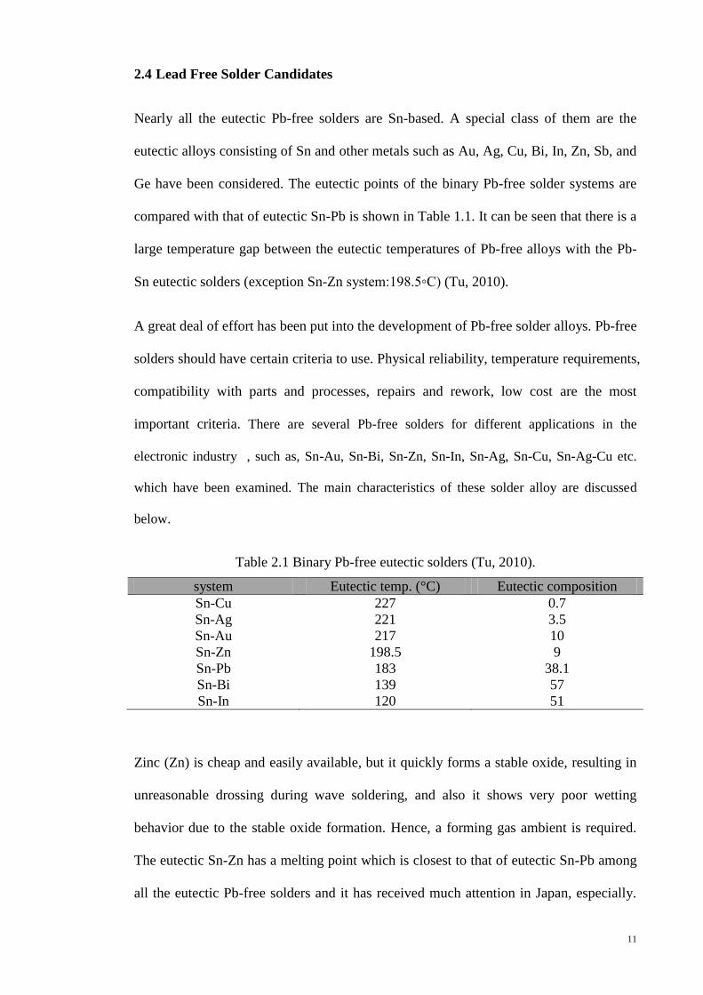
Nearly all the eutectic Pb-free solders are Sn-based. A special class of them are the
eutectic alloys consisting of Sn and other metals such as Au, Ag, Cu, Bi, In, Zn, Sb, and
Ge have been considered. The eutectic points of the binary Pb-free solder systems are
compared with that of eutectic Sn-Pb is shown in Table 1.1. It can be seen that there is a
large temperature gap between the eutectic temperatures of Pb-free alloys with the Pb-
Sn eutectic solders (exception Sn-Zn syste :198.5◦C) (Tu, 2010).
A great deal of effort has been put into the development of Pb-free solder alloys. Pb-free
solders should have certain criteria to use. Physical reliability, temperature requirements,
compatibility with parts and processes, repairs and rework, low cost are the most
important criteria. There are several Pb-free solders for different applications in the
electronic industry , such as, Sn-Au, Sn-Bi, Sn-Zn, Sn-In, Sn-Ag, Sn-Cu, Sn-Ag-Cu etc.
which have been examined. The main characteristics of these solder alloy are discussed
below.
Table 2.1 Binary Pb-free eutectic solders (Tu, 2010).
system Eutectic temp. (°C) Eutectic composition
Sn-Cu 227 0.7
Sn-Ag 221 3.5
Sn-Au 217 10
Sn-Zn 198.5 9
Sn-Pb 183 38.1
Sn-Bi 139 57
Sn-In 120 51
Zinc (Zn) is cheap and easily available, but it quickly forms a stable oxide, resulting in
unreasonable drossing during wave soldering, and also it shows very poor wetting
behavior due to the stable oxide formation. Hence, a forming gas ambient is required.
The eutectic Sn-Zn has a melting point which is closest to that of eutectic Sn-Pb among
all the eutectic Pb-free solders and it has received much attention in Japan, especially.
Page 26
12
Bismuth (Bi) has very good wetting properties. The eutectic Sn-Bi solder has been used
in pin-through-hole technology. However, the availability of Bi could be limited by the
restrictions on Pb, because the primary source of Bi is a by-product in Pb refining. By
restricting the use of Pb, much less Bi will be available. Antimony (Sb) has been
identified as a harmful element by the United Nations Environment Program.
Germanium (Ge) is used only as a minor alloying element of multicomponent solders
due to its reactivity. Indium (In) is too scarce and too expensive to be considered for
broad applications, besides it forms oxides very easily.
A common characteristic of eutectic Sn-noble metal alloys is the high melting point and
high concentration of Sn compared to that of eutectic Sn-Pb. For this reason the reflow
temperature will be higher, by about 40°C. It may increase the dissolution rate and
solubility of Cu and Ni in the molten solder as well as the rate of intermetallic
compound (IMC) formation with Cu and Ni under-bump metallization. If the surface
and interfacial energies are considered, the surface energies of these Pb-free solders are
higher than that of Sn-Pb, so they form a larger wetting angle on Cu, about 35 to 40◦ .
Concerning the microstructure of these eutectic solders, they are a mixture of Sn and
IMC because of the high concentration of Sn, unlike that of eutectic Sn-Pb which has no
IMC. Since metallic Sn has the body-centered tetragonal lattice structure and tends to
deform by twinning, its mechanical properties are anisotropic. The electrical
conductivity of metallic Sn is also anisotropic. The mechanical and electrical properties
of these eutectic solders will be anisotropic, thus the dispersion of the IMC may lead to
the formation of inhomogeneous microstructures, especially in the case of . The
image of appears to be long needlelike crystals in the eutectic Sn-Ag on the
cross-sectional image of a solder joint. But after the matrix of the solder is removed by
deep etching, they turn out to be plate-like.
Page 27
13
2.4.1 Sn-Au
Among all the Pb-free solders, Au-based solder has been found as one of the most
environmental friendly solder and it is being used in the semiconductor industry for the
assembly process (Liu et al., 2008). Au has been ranked among the least toxic elements
by both EPA-US (Environmental Protective Agency-United States) and OSHA
(Occupational and Safety Health Administration). The eutectic 80Au-20Sn solder has
excellent high-temperature performance, superior resistance to corrosion, high electrical
and thermal conductivity and offers fluxless soldering. But, the hardness decreases,
creep penetration and creep strain rate of Au-based solder increase with temperature
(Chidambaram et al., 2010). Beside this, Au-based solder possess acceptable properties
such as suitable melting temperature, good thermal and electrical conductivities, good
fluidity and wettability. However, the alloy system has some problems such as low
ductility and high cost, which prevent its wide application (Takaku et al., 2008).
2.4.2 Sn-Bi
The eutectic Sn-58Bi solder offer a lower melting point than Sn-Pb alloys of 139°C.
The cost of bismuth is almost similar to that of tin (Abtew and Selvaduray, 2000). There
is a problem to supply it because it is a by-product of Pb mining. If a bismuth alloy
picks up any Pb, the melting temperature will drop again with the formation of another
secondary eutectic formed at 96°C (Suraski and Seelig, 2001). Beside this, bismuth
soldering alloys tends to create embrittlement (Wild, 1971). Bismuth alloys also are
prone to failure in peel strength tests due to poor fatigue resistance. Bismuth is also a
poor conductor, both thermally and electrically (Felton et al., 1993).
Page 28
14
2.4.3 Sn-Zn
Zinc is a readily available metal and cheap. The eutectic Sn-9Zn alloy has a low melting
point of 198ºC which is the closest to eutectic Pb-Sn solder among all other lead-free
alternatives (Abtew and Selvaduray, 2000). For this reason, in the recent years the Sn-
9Zn alloy received much attention to the electronic industries. But zinc shows a very
poor wetting behavior with the substrate including poor corrosion resistance in humid or
high temperature environment and forms a stable oxide which keeps its use limited in
the electronic packaging industries (Liu and Tu, 1998, Liu et al., 2008).
2.4.4 Sn-In
The eutectic Sn-52In alloy has a relatively low temperature of 120ºC (Korhonen and
Kivilahti, 1998), which makes this solder suitable for low temperature applications. This
alloy is a good choice for temperature sensitive equipments which are not exposed to
any harsh or high-stress environments. But indium is a rare metal and too expensive to
consider it for board applications (Sharif and Chan, 2005). Furthermore, In alloys
suffers poor corrosion resistance, forms oxide very rapidly during melting and show
strong segregation behavior in the liquid (Korhonen and Kivilahti, 1998).
2.4.5 Sn-Ag
The Sn-4Ag is a rather good alloy and has a long history in the hybrid circuit industries
for electronic packaging applications. But the melting point of this alloy is 221ºC which
is considered higher for many surface mount technology (SMT) applications.
2.4.6 Sn-Cu
The eutectic Sn-0.7Cu is another reliable solder alloy for reflow and wave soldering
applications. The melting temperature of this solder is 227ºC which is undesirable in
Page 29
15
many reflow applications. Moreover, the microstructure of this alloy is prone to whisker
growth because of high Sn concentration (Boettinger et al., 2005). The cost of this
solder is much lower comparing other solders since it does not contain any expensive
elements such as, Ag, Bi or In.
2.4.7 Sn-Ag-Cu
This family of Pb-free Sn-Ag-Cu alloys has shown high promise in the electronic
industries due to having good wetting characteristics with substrate, good fatigue
resistance, good joint strength etc. Owing to these advantages, in 2000 the National
Electronic Manufacturing Initiative (NEMI) recommended to replace eutectic Sn-Pb
solder by near eutectic Sn-Ag-Cu alloys.
Ternary and higher order solders are most likely based on the binary eutectic Sn-Ag,
Sn-Cu, Sn-Zn, or Sn-Bi alloys. The most promising one is eutectic Sn-Ag-Cu. The
eutectic Sn-Ag-Cu alloy forms good quality joints with copper. Its thermo-mechanical
property is better than those of the conventional Sn-Pb solder. Its eutectic temperature
has been determined to be about 217°C, but its eutectic composition has been a subject
of controversy. Based on metallographic examination, differential scanning calorimetry
measurements, and differential thermal analysis results, the eutectic composition was
estimated at , (wt%).
2.5 Thermodynamics of Sn-Ag-Cu Solder Alloy Selection
The phase transformation of Sn-Ag-Cu system is evaluated based on the following
binary systems: Sn-Ag, Sn-Cu and Ag-Cu (Moon et al., 2000). The calculated binary
phase diagrams for the binary system Sn-Ag, Sn-Cu and Ag-Cu are shown in Figure2.4.
Page 30
16
Figure 2.3 Phase diagram of the (a) Sn-Cu (Franke and Neuschütz, 2005), (b) Sn-Ag
(Karakaya and Thompson, 1987) and (c) Ag-Cu system (Xie and Zhang, 1998).
The eutectic temperature of the Sn-Cu system is 227ºC. The eutectic composition is
varied from 0.7 to 0.9 wt% Cu (Moon et al., 2000). The eutectic constituents obtained
from the Sn-Cu phase diagram (Figure 2.3a) are β-Sn and intermetallics. On the
other hand, the eutectic composition of the Sn-Ag system is unanimously taken at 3.5 wt %
of Ag and calculated eutectic temperature is 220.1ºC (Oh et al., 1996).
From the Sn-Ag phase diagram (Figure 2.3b), the eutectic constituents are β-Sn and
intermetallics. Not all binary or ternary elements form the intermetallic compound in
(a)
(b) (c)
Page 31
17
a binary or ternary alloy system. For example, in the Ag-Cu binary system there is no
intermetallic compounds as it is seen in the Figure 2.3c.
These binary phase diagrams are used to understand the melting behavior of ternary Sn-
Ag-Cu alloy. The alloy design criterion for the Sn-Ag-Cu alloy is as follows (Bath, 2010):
01. The liquidus melting temperature of the alloy should be close to the eutectic Sn- Pb
alloy (183ºC) to avoid changing the manufacturing process, materials and
infrastructure.
02. The gap between the solidus and liquidus temperature should be as low as possible
to avoid tombstoning phenomenon and fillet lifting.
03. The solidus temperature of the solder should be significantly higher than the
operating temperature of the solder.
The National Center for Manufacturing Sciences (NCMS), Michigan, USA suggested
that the solder liquidus temperature should be less than 225ºC with a maximum 30ºC
difference between solidus and liquidus temperature (Bath, 2010). Obviously the ternary
eutectic or near eutectic Sn-Ag-Cu alloys meet the first two criterions since the melting
temperature of the ternary eutectic Sn-Ag-Cu alloy is 217ºC (Moon et al., 2000). Depending
on particular applications the operating temperature of electronic equipments may be as
high as 150ºC (Suganuma, 2001). So the ternary eutectic or near eutectic Sn-Ag-Cu alloys
are one of the best candidates for Pb-free solder alternatives. The calculated eutectic
composition of the Sn-Ag-Cu system is 3.66 wt% Ag, 0.91 wt% Cu as it is seen in Figure
2.4. But the experimentally determined value of the Sn-Ag-Cu system is 3.5 wt% Ag, 0.9
wt% Cu which differs a little from the calculated value.
Page 32
18
Figure 2.4 Calculated liquidus surface of the Sn rich region of Sn-Ag-Cu alloy system
(Moon et al., 2000).
2.6 Phase Diagram of Mo with Sn, Ag and Cu
The phase diagrams of Mo with Sn, Ag and Cu are shown in the Figure 2.5(a-c)
respectively. It is seen in the Mo-Sn phase diagram (Figure 2.5a) that Mo has no solubility
in Sn at low temperatures (<300ºC). The calculated results on solubility of Mo in Sn also
show that there is a very negligible solubility of Mo in Sn (Brewer and Lamoreaux, 1980) .
Three intermetallics e.g. and can form in the Mo-Sn system
below 300ºC(Brewer and Lamoreaux, 1980). On the other hand, the Mo-Ag phase diagram
(Figure 2.5b)(Baren, 1990) and Mo-Cu phase diagram (Figure 2.5c)(Subramanian and
Laughlin, 1990) show that Mo has no solubility in Ag and Cu respectively. Besides, it is
also revealed that Mo does not form any compound with Ag and Cu (Subramanian and
Laughlin, 1990).
Page 33
19
Figure 2.5Phase diagram of the (a) Mo-Sn (Brewer and Lamoreaux, 1980) b) Mo-Ag
(Baren, 1990) and (c) Mo-Cu (Baren, 1990).
2.7 Interfacial Reactions of Sn-Ag-Cu Solder with Substrate
During the soldering process, reactions happen between the solder and substrate and
intermetallic compounds (IMCs) form between them. For a good metallurgical bond it
is essential to have a uniform IMC layer between the solder and substrate. However, the
thickness of IMC strongly affects the reliability and mechanical properties of the solder
joint. A thick IMC hamper the interface integrity because of its brittle nature and creates
mismatch in physical properties such as elastic modulus, thermal expansion etc. For this
reason, the interfacial reaction should be controlled to ensure the reliable properties of
(c)
Page 34
20
the solder. The interfacial reaction between the solder and substrate can be categorized
into two groups, namely:
01. Reactions during reflow process,
02. Reactions during high temperature aging.
The former process is encountered during the reflow and wave soldering processes and
the latter happens during service or high temperature aging test.
2.7.1 Microstructure of Interfacial IMCs during reflow
Formation of intermetallic compounds is inevitable during soldering reaction between
the molten solder and substrate. An adequate and uniform intermetallic layer is essential
for a good metallurgical bond between the solder and substrate. But the inherent brittle
nature of interfacial IMCs promotes a brittle failure to the interface (Lee et al., 1997,
Pang et al., 2004b). For this reason, the thickness of the interfacial IMC should be
optimized. During service or high temperature aging the thickness of interfacial IMC
increases due to diffusion of Sn from the bulk solder to the substrate (Sivasubramaniam
et al., 2008).
Solder alloys melt and then react with the substrates to form IMCs, such as Cu6Sn5,
Cu3Sn, Ni3Sn4 and (Cu,Ni)6Sn5 at the solder/substrate interface during soldering
(Laurila et al., 2005). Forming a thin IMC layer by the interfacial reactions is desirable
to achieve a good metallurgical bond; however, excessive IMC growth may have a
harmful effect (Müller, 2004). Therefore aging degradation of the solder joint in
electronic packaging is a critical concern in microelectronic industry. Furthermore, the
addition of certain trace amount alloying elements has strong effects on IMC growth
behaviors (Laurila et al., 2009). For example, the Ni-based substrates were more
effective than Cu in reducing the growth rate of IMCs, as Ni3Sn4 was formed during the
interfacial reactions with Ni-based substrates (Rizvi et al., 2007).
Page 35
21
Both Cu and Ni thin films are used widely as on-chip under-bump metallization (UBM),
but they can be reacted and dissolved away by molten solder during reflow, resulting in
spalling of IMC. Hence, a solder of eutectic composition is undesirable when it is used
with thin-film UBM. It must be supersaturated with excess Cu and/or Ni, about 1%, in
order to reduce the dissolution. Therefore, the recommended composition for Sn-Ag-Cu
solder is about Sn-3Ag-3Cu. While it is off the eutectic composition and will not have a
single melting point, the effect of the composition on melting temperature is very small
and will not be an issue in manufacturing.
2.7.1.1 Sn–Ag–Cu/Cu
Cu is the most common conductor metal, which is utilized in contact with solders owing
to its good solderability characteristic and excellent thermal conductivity performance
(Rizvi, Chan et al. 2006).
The whole interfacial layer of the IMCs will trend to become planar with increasing reflow
time (Moon et al., 2000). The IMC layer are composed of two layers, the light gray regions
are Cu6Sn5 and thin dark gray layer beneath is Cu3Sn, the thickness of which is very thin, as
shown in figure 2.7 (Peng et al., 2007).
Figure 2.6 IMC layers formed between the solder and Cu substrate after soldering
(Zhang et al., 2009).
Figure 2.7 (a) and (b) shows the IMC layers morphology formed between the solder and
Cu substrate after soldering, which presents the interface morphology of the IMCs layer
Page 36
22
under reflow durations (Zhang et al. 2009). The atomic-percentages of Cu and Sn in
Cu6Sn5 phase are 55 and 45, respectively (Kim et al. 2002).
Figure 2.7(a) The microstructure of IMC layer at the interface between solder and Cu
(Zhang et al., 2009). (b) SEM image of typical microstructure of Sn–Ag–Cu solder
I )Sn-rich, II) Cu6Sn5, and III) Ag3Sn (Pang et al., 2004a).
Formation of IMC during the reaction between molten Sn-based solder and Cu
substrate has been reported by a number of studies (Gong et al., 2009, Laurila et al.,
2005). Some of the study also reported the formation of a very thin layer (a few
tens of nanometer) between the Cu6Sn5 IMC and Cu substrate (Gong et al., 2009, Shang
et al., 2009). But after reflow most of the time this thin Cu3Sn layer is not visible under
SEM in the cross-sectional view. In general, for most of the Sn-based solder this newly
form Cu3Sn IMC layer grows at the side of Cu substrate during reflowing (Tu, 2010).
Moreover, Ag3Sn IMC was found dispersed uniformly in the solder after reflow. The planar
Ag3Sn which formed near the interface have changed remarkably and merged together to
large platelets with increasing thermal cycles or aging (Pang et al., 2004a). Large Ag3Sn
needles can cause reliability concern when they form in a high stress concentration area,
such as the corner between solder and copper substrate. Fatigue cracks can initiate and
propagate along the interface between the Ag3Sn and solder matrix, as leading to
mechanical failure (Schoeller et al., 2009).
I
E
M
i
m
a
g
e
o
f
t
y
p
i
c
a
l
m
i
c
r
o
II
E
M
i
m
a
ge
of
ty
pi
ca
l
m
ic
ro
st
r
u
ct
u
re
of
S
III
IE
M
im
ag
e
of
ty
pi
ca
l
mi
cr
os
tr
uc
tu
re
of
Sn
–
A
g–
C
Page 37
23
2.7.1.2 Sn–Ag–Cu/Ni
In electronic products, Ni is one of the most common metals to be in direct contact with
the solders. Nickel is used as a solderable diffusion barrier in several types of surface
finishes for components and printed circuit boards, since the reaction rate of Ni with
molten solder is typically smaller than that of Cu. Therefore, the interactions between
Ni and the Sn-Ag-Cu solders must be understood (Ho et al., 2002).
Sn–Ag–Cu solder reflowed on pure Ni substrates showed distinctly different from those
observed for Sn–Ag–Cu/Cu solder joints, as revealed in Fig.2.8. Instead of Ni3Sn4, it
was determined by means of WDS (Wavelength-Dispersive X-Ray Spectroscopy)
analysis that a different phase was growing at the interface, with a composition of
CuxNiySn45, where the Cu concentration X varied between 44 and 53 atomic percent,
and the Ni concentration y between 1 and 10 atomic percent. These compositions are
consistent with the stoichiometry of the compound (Cu,Ni)6Sn5 (Zribi et al., 2001).
Figure 2.8(a) Interface between Sn-3.0Ag-0.6Cu solder ball and Ni/Cu substrate (b)
Zoom-in view of (a) (Ho et al., 2007).
The reaction between Ni and two solders (Sn3.9Ag0.2Cu and Sn3.9Ag0.6Cu) has been
reported to be very sensitive to the Cu concentration in the solder (C. Ho, et al., 2002).
When Sn3.9Ag0.2Cu reacted with Ni, a continuous (Ni1-xCux)3Sn4 intermetallic layer
formed at the interface. In contrast, when Sn3.9Ag0.6Cu reacted with Ni, a continuous
Fig 2.8 b
Page 38
24
(Cu1-yNiy)6Sn5 intermetallic layer formed. These two compounds, (Ni1-xCux)3Sn4 and
(Cu1-yNiy)6Sn5, are based on the Ni3Sn4 and Cu6Sn5 crystal structures, respectively.
In Figure 2.9 (a) and (b) shows the phase diagram of Cu-Sn and Ni-Sn respectively.
Only a section of the ternary phase diagram of the Cu– Ni–Sn system is available at
235 based on experimental data and thermodynamic modeling as shown in figure
2.9(c) (Korhonen et al., 2000). The (Cu,Ni)6Sn5 band (Ni,Cu)3Sn4 compounds are
presented in this diagram as narrow composition range compounds which extend the
domain of the respective binaries Cu6Sn5 and Ni3Sn4 to a ternary domain. The Cu–Ni–
Sn phase diagram also displays a large two-phase region between (Cu,Ni)6Sn5 and the
Cu–Ni solid solution and a three-phase region between (Cu,Ni)6Sn5 (Ni,Cu)3Sn4, and
the Sn–Cu–Ni solid solution. These observations support the idea of a substitutional
mechanism where atoms such as (Cu and Ni) and (Ni and Au) substitute for each other
in their binary compounds with Sn (Lee et al., 2003).
Both the Cu concentration and the solder volume had a strong effect on the type of the
reaction products (Ho et al., 2006). In detail (Cu,Ni)6Sn5 massively spalled from the
interface under certain conditions, including smaller joints and those with lower Cu
concentration. The massive spalling of (Cu,Ni)6Sn5 was attributed to the decrease of the
available Cu in the solders (Lin and Shih, 2008). The results of this study suggest that
Cu-rich Sn–Ag–Cu solders can be used to prevent this massive spalling.
The evolution of intermetallics are examined at and near SnAgCu/Cu and SnAgCu/Ni
interfaces, and explains that the presence of the Cu in the solder dramatically altered the
phase selectivity at the solder/Ni interface and affected the growth kinetics of
intermetallics. As long as sufficient Cu was available, it would combine with Ni and Sn
to form (Cu,Ni)6Sn5, which grew instead of the Ni3Sn4. This growing phase would,
however, eventually consume essentially all of the available Cu in the solder (Zribi et al.,
Page 39
25
2001). Because the mechanical properties of Sn–Ag–Cu alloys depend upon the Cu
content, this consumption can be expected to alter the mechanical properties of these
Pb-free solder joints.
Figure 2.9 (a) Phase diagram for system Cu-Sn (Franke and Neuschütz, 2005) (b) Phase
diagram of Ni-Sn (Okamoto, 2006) (c) Partial phase diagram of the Cu-Ni-Sn system at
235°C. It can be seen that the (Cu,Ni)6Sn5 compound extends to a wide range of ternary
compositions (Korhonen et al., 2000).
(a)
(b)
(c)
Page 40
26
2.8 Nucleation and Growth of Interfacial IMCs
In the eutectic Sn-Ag-Cu system, the undercooling for the nucleation of the solid Ag3Sn
phase is small, 7.2 °C with differential scanning calorimetry (DSC) in the Sn-3.8Ag-
0.7Cu alloy. But the formation of the Ag3Sn does not facilitate the nucleation of the β-
Sn phase. The β-Sn does not wet on the previously formed Ag3Sn, therefore; it will not
nucleate heterogeneously on the Ag3Sn. The undercooling for the β-Sn phase is 29 °C in
the same alloy. It was observed that the large undercooling of the β-Sn phase in the
presence of large Ag3Sn intermetallic particles and the same conclusion was reached,
that the intermetallics particles are ineffective as heterogeneous nucleation substrates for
Sn (Moon et al., 2000).
The eutectic Sn-3.5Ag, Sn-0.7Cu, and Sn-3.5Ag-0.9Cu alloys are anomalous. The
difference in the melting point between Sn and Ag (or Cu) is large; the difference in the
volume fraction of the constituent phases, β-Sn and Ag3Sn (or Cu6Sn5), is also large.
More importantly, the Ag3Sn and Cu6Sn5 are faceting phases, while β-Sn is a non-
faceting phase. During solidification, the faceting phase, Ag3Sn or Cu6Sn5, grows by
layer deposition involving the lateral propagation of a step across the liquid/solid
interface. On the other hand, the non-faceting phase, β-Sn, advances into the liquid
phase by tree-like, non-faceted dendrites. Because of the different growth mechanisms,
the growth rates of the β-Sn and Ag3Sn (or Cu6Sn5) are quite different. Therefore, the
growths of the β-Sn, and Ag3Sn (or Cu6Sn5) are independent or only loosely coupled
(Shangguan, 2005).
2.8.1 Formation Mechanisms of Interfacial IMCs
The formation of IMC layer is mainly due to the diffusion of atoms from the substrate
into the solder matrix (Yoon et al., 2008). IMCs form instantly at the interface and serve
as the bonding materials between the solder and the substrate as well (Li et al., 2005).
Page 41
27
Transferring through the solder/flux interface was considered as the major mechanism,
which is demonstrated by means of EDX analysis. During wetting, Sn in the solder and
Cu in the substrate begin to move into the flux. The rate of this transport is low because
the ball and the substrate are in solid state. So the transportation zones (TZs) for Sn and
Cu are still very thin and close to the solder and the Cu substrate, as illustrated in Fig.
2.10a. No obvious interfacial reactions were observed. As the temperature increasing
and the solder ball molten, the transfer rate of Cu is still low, and its TZ is still thin and
close to the substrate. In contrast, the transfer rate of Sn from the molten solder is
considerably higher. This results in a much thicker layer of Sn–TZ around the molten
solder ball, as illustrated in Fig. 2.10b. When the Sn–TZ meets with the Cu–TZ, the
formation of reactants was initiated. As shown in Fig. 2.10b, the overlap area
determines the morphology of fine Cu3Sn-particles layer (Gong et al., 2009).
Figure 2.10 Formation mechanism of the fine Sn–Cu particles layer near the three-phase
contact line: a low temperature and b high temperature with the molten solder ball (TZs
transportation zones).
In summary, the surface of Cu is modified by a layer of Cu–Sn IMCs in front of the
three-phase contact boundaries during the wetting process. The liquid solder then
spreads and covers over the existing Cu3Sn layer, forming the Cu6Sn5/Cu3Sn/Cu
sandwich structure interface. To form the Cu3Sn transition zone, both Cu and Sn are
required. Cu can be mainly supplied by the Cu substrate. Sn may transport through the
flux to the transition zone.
Page 42
28
2.9 Effects of Alloying Elements on the Interfacial IMCs
A good deal of work has been done on the interfacial IMCs with the addition of alloying
elements. Based on a summary of the previous research, the addition of alloying
elements to the solder can affect the interfacial IMCs in the following three ways (Zeng
et al., 2010):
1. Alloying elements can increase or decrease the thickness of interfacial IMCs.
2. The physical and chemical properties of the interfacial IMCs can be altered due
to the addition of alloying elements.
3. Additional reaction layer can form at the interface between the solder and
substrate.
Alloying elements can be categorized in two groups on the basis of solubility (Laurila et
al., 2010):
1. Elements that show marked solubility on the Sn-Cu intermetallics, such as Ni,
Co, Au, Sb, In, etc.
2. Elements that do not show marked solubility on the Sn-Cu intermetallics, such
as Al, Bi, P, Ti, S, rare earth elements.
Between alloying elements, Ni and Co has a prominent solubility on the interfacial IMCs. It
is found that the addition of Ni and Co as an alloying element to the solder increases the
total IMC thickness but the Cu3Sn IMC thickness is decreased during reflow and aging
compared to the pure solder (Wang et al., 2009). It is observed that the addition of Au (less
than 0.25 wt %) to the near eutectic SAC solder results scallop type (Cu,Au)6Sn5 IMC after
reflow. However, if the Au content is more than 0.25 wt% the morphology of the interfacial
IMC is changed with the formation of two phase layer [((Cu,Au)6Sn5)+Sn] (Park et al.,
2003). The addition of Au reduces the Cu3Sn IMC, but the effect of Au is weaker compared
Ni and Co because of having lower solubility in Cu3Sn IMC (Zakel et al., 1991). On the
Page 43
29
contrary, though Sb has a strong effect on solid solution strengthening of Sn, it has virtually
no effect on the interfacial IMC (Laurila et al., 2010).
Addition of elements that do not show marked solubility on the interfacial Cu-Sn IMC
like Al is found to increase the mechanical properties such as microhardness, strength
etc. to the SAC solder (Liu et al., 2008).
2.10 Effects of Nanoparticles on Interfacial IMC
In recent research, Nano-composite solders are being investigated specially for cases
where better creep and fatigue resistance are required (Shen and Chan, 2009). Several
methods such as ball milling, paste mixing, mixing with molten solder alloy, in-situ
method have been developed for mixing nanoparticles with the solder (Hwang et al.,
2003, Lin et al., 2002, Shen and Chan, 2009). Refinement of solder microstructure
resulting from nanoparticle addition has been reported in a number of studies (Kumar et
al., 2008, Shen et al., 2006). The effect of Co, Ni, Pt, Al, P, Cu, Zn, Ge, Ag, In, Sb and
Au nanoparticles Studied on the interfacial IMC between Sn–3.0Ag solder and organic
solderability preservative (OSP) Cu pads during reflow and aging process. It was also
found that nanoparticles of Co, Ni and Pt are effective in influencing the growth of
interfacial IMC layer between Sn-based Pb-free solder and Cu substrate after
reflow(Amagai, 2008). Recent results show that Co and Ni nanoparticles impart their
effect on the interfacial IMC through alloying effect (Amagai, 2008, Haseeb and Leng,
2011). With the addition of Co and Ni nanoparticles to the SAC solder the total
thickness of interfacial IMC increases but the thickness of Cu3Sn IMC decreases
(Haseeb and Leng, 2011). Extent of alloying effect of nanoparticles is related to the
solubility of that particular element into the solder (Laurila et al., 2010).
Reported results of inert nanoparticles addition to Sn-based solder such as Al2O3,SiC,
TiO2, carbon nanotube shows refinement bulk microstructure and improvement of the
Page 44
30
mechanical properties such as micro hardness (Shen and Chan, 2009). Inert
nanoparticles are considered as a surface active material since they gather at the grain
boundaries of the solder matrix and do not react with the solder. Surface absorption
theory can be applied to explain the controlling mechanism of the suppression of
interfacial IMC due to the addition of inert nanoparticles. According to the theory, the
surface free energy of a whole crystal is:
∑
∑
∑
∫
(2.2)
Where, is the adsorption of surface-active material at crystal planes k, c is the
concentration of the surface-active material, R is the ideal gas constant, T is the absolute
temperature, is the surface tension of crystal planes k with adsorption of the active
material, is the surface tension of the initial crystal planes k without adsorption,
and is the area of the crystal planes k.
The net value of the right hand side becomes lower with increasing the value . This
implies that the surface free energy of the whole crystal plane would decrease with the
maximum amount of adsorption, . Thus, an increase in the amount of elements
adsorbed decreases its surface energy and, therefore, decreases the growth velocity of
this crystal plane (Shen and Chan, 2009). Generally, crystal planes having higher
surface energy grows rapidly. But the surface energy is deceased when surface active
materials are absorbed at the crystal plane. As the amount of absorption of surface
active material is increased, the growth velocity of the crystal plane is decreased.
The explanation in surface absorption theory is qualitative, thus this theory is not
universally accepted to explain the effect of inert nanoparticles on the interfacial IMC.
There are several factors that affect the growth process of interfacial IMCs, such as
Page 45
31
substrate dissolution, grain boundary diffusion, grain coarsening, grain boundary
grooving etc., into the molten solder (Schaefer et al., 1998). So this is particularly
important to investigate the distribution, locations, reactions of the nanoparticles into
the solder during reflow (Shen and Chan, 2009).
2.11 Electrodeposition of Nickel
Nickel electroplating is a commercially important and versatile surface-finishing
process. Its commercial importance may be judged from the amount of nickel in the
form of metal and salts consumed annually for electroplating, now roughly 100,000
metric tons worldwide, as well as its versatility from its many current applications
(DiBari, 1996).
Nickel electroplating is similar to other electrodeposition processes that employ soluble
metal anodes; that is, direct current is made to flow between two electrodes immersed in
a conductive, aqueous solution of nickel salts. The flow of direct current causes one of
the electrodes (the anode) to dissolve and the other electrode (the cathode) to become
covered with nickel. The nickel in solution is present in the form of divalent, positively
charged ions ( ). When current flows, the positive ions react with two electrons
(2 ) and are converted to metallic nickel ( ) at the cathode surface. The reverse
occurs at the anode where metallic nickel is dissolved to form divalent, positively
charged ions which enter the solution. The nickel ions discharged at the cathode are thus
replenished by those formed at the anode (Schlesinger, 2010).
The amount of nickel deposited at the cathode and the amount dissolved at the anode
are directly proportional to the product of the current and time and may be calculated
from the expression (Faraday’s Laws):
m=1.095 (2.3)
Page 46
32
Where m is the amount of nickel deposited at the cathode (or dissolved at the anode) in
grams, I is the current that flows through the plating tank in amperes, t is the time that
the current flows in hours, and a is the current efficiency ratio. The cathode efficiency
of different nickel plating solutions may vary from 90 to 97% and, accordingly, a will
vary from 0.90 to 0.97. Because the anode and cathode efficiencies are not exactly equal,
the nickel ion concentration and the pH of the solution will slowly increase as plating
proceeds.
2.11.1 Average Coating Thickness
An expression for calculating nickel thickness, s in micrometers, can be derived by
dividing Eq. (2.4) by the product of the density of nickel, d (8.907 g ), and the
surface area to be electroplated, A, and multiplying by 100 to obtain the thickness in
micrometers:
(2.4)
The ratio I/A is the current density and thus the above expression shows that the coating
thickness depends on the current density and time, whereas the amount or mass of
nickel deposited, Eq. (2.4), depends on the current and time. Equation (2.4) is the basis
for the electrodeposition data compiled in Table 2.2, which gives the time in minutes
required to deposit a nickel coating of specified thickness at different values of current
density. The expression above and Table 2.2 provide a means of estimating the average
coating thickness.
Page 47
33
Table 2.2 Nickel Electrodeposition Data (Mordechay Schlesinger, 2010)
Deposit
thickness
(µm)
Weight
per Unit
Area(g
Ampere
Hours
per Unit
(Ah
d
Times (min) to obtain Deposit at Various Current Densities (Ah
d
0.5 1 1.5 2 3 4 5 6 8 10
2 0.18 0.17 20 10 6.8 5.1 3.4 2.6 2.0 1.7 1.3 1
4 0.36 0.34 41 20 14 10 6.8 5.1 4.1 3.4 2.6 2
6 0.53 0.51 61 31 20 15 10 7.7 6.1 5.1 3.8 3.1
8 0.71 0.68 82 41 27 20 13 10 8.2 6.8 5.1 4.1
10 0.89 0.85 100 51 34 26 17 13 10 8.5 6.4 5.1
12 1.1 1.0 120 61 41 31 20 15 12 10 7.7 6.1
14 1.2 1.2 140 71 48 36 24 18 14 12 8.9 7.1
16 1.4 1.4 160 82 54 41 27 20 16 14 10 8.2
18 1.6 1.5 180 92 61 46 31 23 18 15 11 9.2
20 1.8 1.7 200 100 68 51 34 26 20 17 13 10
40 3.6 3.4 410 200 140 100 68 51 41 34 26 20
2.11.2 Functional Electroplating and Deposit Properties
Electrodeposited nickel coatings are applied in functional applications to modify or
improve corrosion resistance, hardness, wear, magnetic, and other properties.
The main constituents in Watts’s solutions affect the properties of electrodeposited
nickel. Nickel sulfate improves conductivity and metal distribution and determines the
limiting cathode current density for producing sound nickel deposits. Nickel chloride
improves anode corrosion but also increases conductivity, throwing power, and
uniformity of coating thickness distribution. In addition chlorides increase the internal
stress of the deposits, and they tend to refine grain size and minimize formation of
nodules and trees. Boric acid is added for buffering purposes and affects the appearance
of the deposits. Deposits may be cracked and burnt at low boric acid concentrations.
Anionic wetting agents or surfactants that lower the surface tension of the plating
Page 48
34
solution so that air and hydrogen bubbles do not cling to the parts being plated are
almost always added to control pitting and, by eliminating porosity, have an indirect
effect on corrosion performance.
Table 2.3 Nickel Plating Solutions (Mordechay Schlesinger, 2010).
Ele t ol te Co ositio L 1
Solution Watts Nickel Nickel
Sulfamate
Basic
Semibright
Bath
Nickel sulfate,
225-400 - 300
Nickel
Sulfamate, - 30-45 -
Nickel choloride,
30-60 300-450 35
Boric acid, 30-45 0-30 45
Operating Condition
Temperature(°C) 44-46 32-60 54
Agitation Air or
mechanical
Air or
mechanical
Air or
mechanical
Cathode current
density( 3-11 0.5-30 3-10
Anodes Nickel Nickel Nickel
PH 2-4.5 3.5-5.0 3.5-4.5
Mechanical Properties
Tensile strength(MPa) 345-435 415-610 -
Elongation (%) 10-30 5-30 8-20
Vickers hardness( 100 g
load) 130-200 170-230 300-400
Internal stress(MPa) 125-185 0-55 35-150
Operating conditions, such as pH, temperature, current density and chloride content,
affect the properties of deposits from Watts solutions. Table 2.3 shows the properties of
nickel Plating Solutions.
2.12 Summary and Conclusion
Several challenges should be met before the lead-based solders are utterly replaced by
the lead-free solders in the microelectronic packaging. The trend of miniaturization and
functional density enhancement requires much smaller solder joints with a fine pitch
Page 49
35
interconnection. These ultra-fine solder joints lead to high homologous temperature
during services which may lead to coarsening of the microstructure at the
solder/substrate interface. The key issue to ensure a fine and uniform solder joint
microstructure is to slow down the interfacial reactions between the solder and substrate.
Numerous solders have been studied by researchers worldwide. Most is focused on the
bulk microstructure and mechanical properties with and without the addition of
additives. Some research concentrate on the addition of alloying elements and
nanoparticles to the lead-free solder. It was found from the previous research that
addition of Fe, Co, Ni as an alloying element to the solder increases the intermetallic
compound formation at the solder/substrate interface. Beside, nanoparticles of Co and
Ni also show a similar trend of increasing the intermetallic compound thickness.
Addition of inert nanoparticles such as TiO2, Al2O3, CNTs focus only the bulk
microstructure and mechanical properties of the solder. No research has been done on
the interfacial IMC with the addition of inert metallic nanoparticles.
Previous studies showed that the addition of Mo nanoparticles to SAC solder causes a
decrease in the thickness and diameter of interfacial Cu6Sn5 scallops (Haseeb et al.,
2012). In this research the interaction between SAC solder in the presence of Mo
Nanoparticle and electroplated cu substrate with Ni is studied.
Page 50
36
Chapter 3: Methodology
3.1 Raw Materials and Characterization
In this study, molybdenum nanoparticle (99.8% trace metal basis) was used as a
reinforcing material with the Sn-3.8Ag-0.7Cu (SAC) solder paste (Indium Corporation
of America). The particle size of the SAC solder paste was investigated from scanning
electron microscopy (SEM, Philips XL-40) image. First by using propanol, flux from
the solder paste was removed. Then a small amount of solder sample was taken in a
sample holder and dried at 100ºC for one hour in an oven. Finally the dried solder was
analyzed under SEM.
The morphology and size of the Mo nanoparticles were determined by using a Philips
CM200 transmission electron microscopy (TEM). Firstly, a small amount of Mo
nanoparticles were dispersed into distilled water onto a carbon film supported by copper
grids. The grain size measurement and phase analysis of Mo nanoparticles was
conducted by X-Ray diffractometer (XRD). The nanoparticles were exposed to
( =0.15406 nm) radiation with a scanning speed of 2º/min in the 10-80º diffraction
range with a step size of 0.05º.
3.2 Sample Preparation and Treatment
3.2.1 Preparation of Copper Substrate with Electroplated Ni
Commercial polycrystalline copper sheets (30mm×30mm×0.3mm) were used for the
preparing of the solder joint. Prior to electroplating, the sheets were cleaned by
detergent followed by dipping in 10 remove oxide after that the sheets
were rinsed thoroughly in distilled water followed by cleaning with acetone. After the
Page 51
37
cleaning, Watts’s Nickel plating bath was used to electroplate Ni on copper substrate.
The plating solutions with plating parameters are shown in Table 3.1.
Table 3.1 Plating solution and parameters for the deposition of Ni on Cu substrate
(Mordechay Schlesinger, 2010).
Type Composition(g ) pH Temperature
(°C)
Cathode
current
density
Watts nickel
Nickel sulphate
,300
Boric acid ,35
Nickel chloride
,45
3.5 55 50
The condition that is mentioned in Table3.2 is used to electrodeposit Ni with10
thickness on Cu substrate.
Table 3.2 Nickel electroplating data(Mordechay Schlesinger, 2010)
De osit i kel
𝝁𝒎
Wei ht e
u it a ea
𝒈𝒅𝒎
A e e hou s
e u it
𝑨𝐡 𝒅𝒎
Ti e i to obtai
de osit with 𝟓𝟎 𝒎𝑨 𝒎 u e t
de sit
10 0.89 0.85 10
3.2.2 Preparation of Composite Solder Paste and Nanoparticles Distribution
Mo nanoparticles were mixed manually with Sn-3.8Ag-0.7Cu (SAC) solder paste for
nominal compositions of 1and 3 wt%. A homogeneous paste composition was obtained
by 30 min mixing. The distribution of Mo nanoparticles in the SAC solder paste was
found by taking small amount composite paste to a SEM sample holder. Then it was
placed in an oven and heated at 100ºC for one hour to dry the paste composition. After
that, the dry composite paste was analyzed by high resolution field emission scanning
electron microscopy (Zeiss Ultra-60 FESEM) and energy-dispersive X-ray spectroscopy
(EDX, EDAX-Genesis Utilities) to check the distribution of Mo nanoparticles into the
SAC solder.
Page 52
38
3.2.3 Preparation of Reflowed Samples
Prepared copper substrate with electroplated Ni layer is rinsed thoroughly in distilled
water and finally cleaned with acetone. After the surface preparation the composite
solder paste was placed on the copper substrate through a mask having an opening
diameter of 6.5mm and 1.24mm thickness (JIS Z3198-3, 2003). Then the composite
solder paste was reflowed on a hot plate at 250ºC for 45 s.
3.2.4 Multiple Reflow
After first reflow one set of samples were reflowed again in a reflow oven (Forced
convection, FT02) for six times at 250ºC for 45s. After reflow, the solders were cleaned
with acetone to remove the flux residue. The multiple reflowed samples were also cross
sectioned, mounted in epoxy and polished by employing the standard metallographic
techniques. The cross-sectional view of the interfacial IMC was observed by
backscattered electron detector under a field emission scanning electron microscope
(FESEM). The elemental analysis was carried out by using energy dispersive X-ray
spectroscopy (EDX). To expose the top surface of the intermetallic compound, samples
were chemically etched for 24h as it is mentioned previously. In this case also the
microstructure was observed by high resolution field emission SEM (Zeiss Ultra-60
FESEM). The elemental analysis was carried out by energy-dispersive X-ray
spectroscopy (EDX, EDAX-Genesis Utilities).
3.3 Characterization of Solder
3.3.1 Differential Scanning Calorimetry Measurement of Solder Paste
Differential scanning calorimetry (DSC, Mettler DSC 820, Switzerland) measurements
were conducted to find out the melting temperatures of the composite solder pastes.
Page 53
39
Samples were weighted by a microbalance (~10-15mg). Then the samples were placed
on a 70 l platinu crucible inside the DSC furnace and heated to 250ºC at a heating
rate of 10ºC/min. The onset temperature in the DSC curve was taken as the melting
point of the solders.
3.3.2 Inductively coupled-Optical Emission Spectrometer
The solder samples were chemically analyzed by inductively coupled-Optical Emission
Spectrometer (ICP-OES, Perkin Elmer Optima 2000 DV) to find out the actual amount
of molybdenum content in the solder. After reflow, the flux residue on top of the solder
matrix was removed by hexane. The solders were scratched out using tweezers. After
that 0.5g of flux residue and solders were digested in 5 ml concentrated hydrochloric
acid (HCl) separately and then diluted to 100 ml deionized water. The calibration
standard solution of Mo (Cat No. 1.70227.0500, Merck) were prepared from the 1000
ppm stock solution. Each calibration curve was created using three standard
concentration curves (2, 4 and 6 ppm). The concentration of Mo inside the solder and
flux was indicated by the intensity of the emission.
3.3.3 Spreading Rate and Wetting Angle
The ability of the molten solder to spread over the substrate is used to measure the
wetting behavior. After first reflow, twelve samples were utilized to calculate the spread
rate according to the Japanese Industrial Standard (JIS Z3198-3, 2003). According to
the Japanese Industrial Standard, the spread rate was calculated by the following
equation
(3.1)
⁄ (3.1)
Page 54
40
Where, SR = Spread rate (%), H = Height of the spread solder (mm), D = Diameter
when the solder used for a test is considered as a ball (mm) and V = Mass/density of the
solder sample used for the test = 7.5 gm/cm3.
After calculating the spreading rate, the solder samples were cross sectioned, mounted
in epoxy and polished up to 0.02 m finish by employing standard metallographic
technique for measuring the wetting angle by optical microscope.
Page 55
41
Chapter 4: Results and Discussion
4.1 Characterization of Raw Materials
4.1.1 Morphological Characterization and Particle Sizes of Solder Paste
Mo nanoparticles used in this study were characterized in an earlier study (Arafat, 2012).
Figure 4.1 shows the scanning electron microscopy (SEM) image of Sn-3.8Ag-0.7Cu
(SAC) solder balls in the solder paste. Flux was removed from the SAC solder paste by
dissolving it in propanol. It was seen that shape of the SAC solder balls was spherical
with a small variation in diameter. The average diameter of the solder balls calculated
from Figure 4.1 was 34±6µm.
Figure 4.1 SEM image of SAC solder powder (Flux has been removed) (Arafat, 2012).
4.1.2 TEM of Mo Nanoparticles
Figure 4.2 shows a transmission electron microscopy (TEM) micrograph and the
particle size distribution of Mo nanoparticles. More than 250 particles were used for
calculating particle size distribution. It is found from the distribution that the size of the
most particles is in between 20-100 nm, although some particles are as big as 200 nm.
Page 56
42
But the frequency of the particles having size more than 200 nm is quite low. The
weighted average of the size distribution shows that the average size of Mo
nanoparticles is 70 nm.
Figure 4.2 (a) TEM micrograph of the Mo Nano-particles, (b) Histogram of particle size
(Arafat, 2012).
4.1.3 X-Ray Diffraction of Mo Nanoparticles
The XRD pattern of the Mo nanoparticles is demonstrated in Figure 4.3. Three strong
peaks at 40.509º, 58.599º and 73.660º clearly indicates the presence of (110), (200) and
(211) crystal plane in Mo nanoparticles respectively. It may be noted that no oxide peak
was observed from the XRD pattern. The grain size of Mo nanoparticles was calculated
by using the Scherrer’s Equation. 4.1.
4.1)
Where K is the shape factor, λ is the X-ray wavelength, β is the line broadening at half
the maximum intensity (FWHM) in radians, and θ is the Bragg angle. L is the mean size
of the ordered (crystalline) domains, which may be smaller or equal to the grain size.
(a) (b)
Page 57
43
The Scherrer’s equation was corrected by assu ing the para eter β as a Gaussian
function for the diffraction peaks and instrumental broadening. The average grain size
of Mo nanoparticle was found around 40 nm.
Figure 4.3 X-Ray diffraction (XRD) pattern of Mo nanoparticles (Arafat, 2011).
4.2 Distribution of Mo Nanoparticles in the SAC Solder Paste
The spatial distribution and elemental mapping of the solder paste nominally containing
2 wt% Mo is shown in Figure 4.4. Figure 4.4(a) shows an overall view of the paste at a
lower magnification. It is seen in Figure 4.4(a) that tiny Mo nanoparticles adhere to the
surface of large SAC solder balls. Mo nanoparticles were also seen in the flux situated
at the crevices between SAC balls. High magnification images provide clean views of
both SAC ball surface (Figure 4.4c) and flux (Figure 4.4d). It is observed that Mo
nanoparticles are fairly well distributed in the paste.
Page 58
44
Figure 4.4FESEM images of solder paste after blending, nominally containing 2 wt% of
Mo nanoparticles (a) distribution of Mo nanoparticles into the solder paste, (b)
elemental mapping of the composite paste showing Mo (red), Sn (cyan), Ag (blue), and
Cu (yellow), (c) high resolution image focused on the solder ball surface and (d) high
resolution image focused on the flux (Arafat et al., 2011).
4.3 Chemical Analysis of the Reflowed Samples
Upon reflow, the solder balls melted, coalesced and formed the solder joint. The flux
residue stays on the surface of the solder joint. In order to find out how much Mo
nanoparticles is retained in the solidified solder, the latter was chemically analyzed by
inductive coupled plasma-optical emission spectroscopy ICP-OES. The actual Mo
content of the solder is shown in the Table 4.1. For the nominal addition of 1 and 3 wt%
of Mo nanoparticles into the solder paste, the actual content in the solder is found to be
only 0.04 and 0.14 wt% of Mo respectively. The rest of the Mo enters in the flux residue
(Arafat et al., 2011). Hereafter, solders actually containing 0.04 and 0.14 wt % Mo will
Page 59
45
be designated as (SAC + 0.04 n-Mo) and (SAC + 0.14 n-Mo) respectively with n
referring to nanoparticles.
Table 4.1 Molybdenum content of solders analyzed by ICP-OES after reflow.
Nominal Mo Content, wt
%
Actual Mo content in the
solder, wt %
Actual Mo content in
the flux, wt %
1.0 0.04 5.40
3.0 0.14 -
It may be noted that the solder paste consists of a flux in which SAC solder balls were
dispersed. After the addition and mixing of nanoparticles, the Mo nanoparticles also
dispersed within in the flux remaining in between the SAC balls (Figure 4.4). During
reflow process, a fraction of the nanoparticles enters the molten pool of solder and
eventually got trapped inside the solidified solder mass. The rest stays with the flux
residue. Similar result was obtained for Co nanoparticles (Arafat et al., 2011).However,
in the case of Co nanoparticles, the fraction of nanoparticles retained in the solder was
higher. The incorporation of nanoparticles into solder will mainly depend on the
interactions between nanoparticles and the solder. It has been suggested that a
reinforcing particle can be pushed (rejected), engulfed or entrapped at the particle-liquid
metal interface depending upon the interaction mechanisms(Dhindaw, 1999, Wilde and
Perepezko, 2000). The incorporation of a lower amount of Mo in SAC suggests that Mo
nanoparticles experiences rejection by the liquid SAC interface to a greater extent. Poor
wetting of Mo and SAC could be a reason for higher rejection. In spite of the rejection,
the amount of Mo nanoparticles still retained in the solder has definite influence on
interfacial IMC growth characteristics as will be discussed later. This simple paste
mixing method to incorporate nanoparticles into the solder is gaining increasing
attention by the researchers nowadays. Reported results on sample prepared by paste
mixing method also show that enough nanoparticles can be incorporated to the solder to
enhance its properties(Tai et al., 2005). On the other hand this method can be used in
Page 60
46
the conventional reflow process using the existing industrial infrastructure(Zerrer et al.,
2008).
4.4 Spreading Rate and Wetting Angle
Figure 4.5 shows the spreading rate and wetting angle of the Mo added nanocomposite
solder as a function of nanoparticles content. The spreading rate drops from 74.22%to
66.34% for (SAC + 0.14 n-Mo) solder (Figure 4.5 a). On the other hand the wetting
angle increases from 17.3º to 28.9º to the (SAC + 0.14 n- Mo) (Figure 4.5.b).
Figure 4.5 (a) Spread rate and (b) wetting angle as a function of wt % of Mo
nanoparticles.
Actually, spreading rate and wetting angle are used to measure the solderability of the
composite paste. For good metallurgical bond between solder and substrate, the
spreadability and wettability should be in acceptable range. It is generally agreed that
higher spreading rate with a lower wetting angle is desired during reflow. With
increasing Mo nanoparticles up to 0.1 wt % into the SAC solder paste the spreading rate
decreases from 74.22%to 66.34% but the wetting angle increases from 17.3º to 28.9º
However Mo nanoparticles-added SAC solder shows a considerable solderability
comparing the SAC and Sn-Pb solder(Wang et al., 2008a). Reported results of wetting
angle by wetting balance technique for Sn-Pb solder on Cu substrate was found 20º
50
55
60
65
70
75
80
85
90
95
100
0 0.05 0.1 0.15
spre
adin
g ra
te(%
)
Wt% Mo nanoparticle
(a)
0
5
10
15
20
25
30
0 0.05 0.1 0.15
wet
tin
g an
gle
(deg
ree)
Wt% Mo nanoparticle
(b)
Page 61
47
(Wang et al., 2008a). The possible reason for decreasing spreading rate could be due to
the increase of melt viscosity for addition of nanoparticles into solder paste. Increased
amount of nanoparticles inhibits the molten composite solder to flow on the
substrate(Nai et al., 2006). Inhibition to flow of the composite melt on the substrate is
believed to lead higher wetting angle compare with SAC solder.
Arafat (2012) showed that the spreading rate of SAC+0.14n-Mo on Cu substrate
decreased from 79.8 to 76.8% and wetting angle increased from 17.8° to 28.8°. In
comparison it is seen that for Ni substrate, the spreading rate decreased from 74.22%to
66.34% and wetting angle increased from 17.3º to 28.9º upon the addition of 0.14 % Mo
nanoparticle (Figure 4.5).
4.5 Analysis of Electroplated Ni on Copper Substrate
The FESEM image in Figure 4.6 illustrates the thickness of electroplated Ni on copper
substrate. On the basis of electroplating condition mentioned in Tables 3.1 and 3.2,
theoretically the thickness should be 10µm. EDX confirms that dark contrast layer with
homogenous uniform morphology is Ni. The measurement of this layer on all samples
show that the avarage Ni thickness is 6.5±0.5µm. The lower thickness would be due to
lower current efficiency of Ni plating.
Figure 4.6 SAC on copper substrate with a top layer of electroplated Ni.
6.5 µm Electroplated Ni
Cu
SAC solder
Page 62
48
4.6 IMC Morphology on Ni and Cu Substrate
FESEM results show the IMC morphology of SAC and SAC+ 0.14 n-Mo on Cu and Ni
substrate in Figures 4.7. The IMC at the interface between SAC and Cu substrate has
scallop shape, in Figure 4.7a and 4.7b but 0.14 n-Mo in 4.7b decrease the size of scallop.
It is shown in Figure 4.7b that there are existed 2 layers of IMC (points Y and Z) at
interface and one IMC inside the bulk of the SAC solder (point X). Figure 4.7c and 4.7d
show flat shape IMC at the Ni substrate, adding 0.14 n-Mo (4.7d) decreased the
thickness. The Figure 4.7c shows the one layer of IMC at interface ( ) and 2 kind
of IMC inside the bulk of SAC solder (
Figure 4.7 IMC morphology of (a) SAC on Cu substrate after 1st reflow, (b) SAC+0.14
n-Mo on cu substrate after 1st reflow (c)SAC on Ni substrate after 1
st reflow (d) SAC
+0.14 n-Mo on Ni substrate after 1st reflow.
Figure 4.8 shows the EDX at the interface between SAC+0.14 n-Mo on Cu substrate, it
reveals that the IMC at point Y is . Figure 4.9 demonstrates and
IMC on the copper substrate. The EDX result in figure 4.10 shows the compound at
(b)
(c) (d)
Y
Z
(a)
Page 63
49
point ( ), and the Figure 4.11 illustrate the intermetallic compound at
interface and in the bulk of the solder on Ni substrate. On all samples, the composition
of , and was confirmed by EDX. Mo nanoparticle was
not detected in cross sectional view but detected in top view (Arafat, 2012).
Figure 4.8 EDX result at the interface between Cu substrate and SAC solder (point Y).
Figure 4.9SAC+ 0.14 n-Mo after 6th
reflow on copper substrate.
Figure 4.10 EDX result at the interface between Ni layer and SAC solder (point ).
Y
Cu
Page 64
50
Figure 4.11 Intermetallic compound between the SAC solder and the Ni substrate.
4.7 Effect of Mo Nanoparticles on IMC
Figure 4.12 shows the cross sectional backscattered electron micrographs of SAC, (SAC
+ 0.04 n-Mo) and (SAC + 0.14 n-Mo) after first and six reflow on Ni substrate.
Formation of IMC between the solder and Ni substrate is clearly visible.
A comparison between Figures 4.12a, 4.12b and 4.12c show that the addition of Mo
nanoparticles results in a decrease in overall IMC thickness after first reflow. The effect
of Mo nanoparticles is evident after six times reflow as well (Figures 4.12d, 4.12e and
4.12f). No molybdenum could be detected inside the (Cu,Ni)6Sn5 IMC by EDX analysis
for both first time and six times reflow.
The thickness of the interfacial IMC increases with an increase in the number of reflow
for both SAC and Mo nanoparticle added SAC solder. But the thickness of the
interfacial IMC is lower, first the Ni layer on copper in compare to the Cu substrate
decrease the IMC thickness because the Ni works as the barrier and prevent Cu to
diffuse inside the IMC and increase its thickness, second the Mo nanoparticles-added
solder compared with the SAC solder can decrease the IMC thickness too .The IMC
thickness in SAC+0.14n-Mo on copper after first reflow is around 2.02µm and Ni
Ni
Page 65
51
substrate is 0.51µm, it is clearly shows the effect of Ni substrate to decrease the IMC
thickness.
Figure 4.13 shows the effect of different percent of Mo Nanoparticle on IMC thickness
on SAC solder after 1st reflow and 6th
reflow on Ni substrate. Lower IMC thickness is
observed for all Mo nanoparticles-added samples.
Figure 4.12Backscattered electron micrographs of the cross sectional view (a) SAC after
first times reflow, (b) (SAC + 0.04 n-Mo) after first times reflow, (c) (SAC + 0.14 n-Mo)
after first times reflow ,(d) SAC after six times reflow and (e) (SAC + 0.04 n-Mo) after
six times reflow(f) (SAC + 0.14 n-Mo) after six times reflow (All has same
magnification of 4.00 KX).
Figure 4.13 Effect of Mo nanoparticles on the IMC thickness.
0
0.2
0.4
0.6
0.8
1
1.2
Pure SAC SAC+0.04Mo SAC+0.14 Mo
IMC
th
ickn
ess
(µm
)
1st reflow
6th reflow
a
f e d
c b
Page 66
52
4.7.1 State of Mo Nanoparticles during Reflow
The exact mechanism(s) of the Mo nanoparticles to suppress the growth of interfacial
IMC thickness and scallop diameter is not obvious. However, several cases are
speculated. In one case, nanoparticles may remain as discrete, unaltered particles during
reflow. On the other one, they can be completely consumed in some reaction(s) or
through dissolution within the molten solder. Actual alteration that the nanoparticles
may undergo will depend on a number of factors, including their melting point and
chemical interaction(s) with the solder. Molybdenum has a relatively high melting point
(2623ºC) compared with the reflow temperature (250ºC) used in this study. So, under
the present experimental condition, Mo nanoparticles are not expected to physically
melt during reflow. Referring to the Mo- Sn phase diagram, Mo has negligible solubility
in Sn. The phase diagram shows that as many as three IMCs e.g., Mo3Sn,
Mo2Sn3/Mo3Sn2, and MoSn2 can exist in the Mo-Sn system(Brewer and Lamoreaux,
1980). But no evidence of Mo-Sn compound formation was found on Mo nanoparticles
by EDX. It may be noted that Mo does not form any compound with Cu and Ag at
250ºC, and has no solubility in these elements (Baren, 1990, Subramanian and Laughlin,
1990).
4.7.2 Suggested Mechanism for Retardation of IMC Growth by Mo Nanoparticles
When Mo nanoparticles are mixed with SAC solder paste and reflowed at 250ºC, they
remain as stable solid particles. The nanoparticles do not particularly undergo any kind
of chemical reactions or dissolution. So the retardation of IMC growth and scallop
diameter are solely due to the particle effect of Mo nanoparticles. There can be three
possibilities through which Mo nanoparticles can lower the thickness and reduce the
diameter of IMC scallop:
Page 67
53
a. Mo nanoparticles can act as heterogeneous nucleation sites for the
formation of (Cu,Ni)6Sn5 nucleus. This can increase the density of
nucleation of (Cu,Ni)6Sn5 grains,
b. Mo nanoparticles may have pinning effect on the growing front of
(Cu,Ni)6Sn5 scallops, and
c. Both (a) and (b).
For a particle to act as a heterogeneous nucleation site, the interfacial energy between
the liquid and solid particles should be low. In other words, the wetting angle of the
liquid at the solid surface should be low. No data on the interfacial energy and wetting
angle between liquid (Cu,Ni)6Sn5 and Mo is available in the literature. If the Mo
nanoparticles act as heterogeneous nucleation sites, it is likely that the nanoparticles
could be formed as inclusions in the (Cu,Ni)6Sn5 scallops. Extensive examination of
multiple samples on cross-section under high resolution FESEM could not identify any
such inclusion. These lead on to suggest that Mo nanoparticles are unlikely to act as
heterogeneous nucleation sites. It is therefore believed that the influence of Mo
nanoparticles on the (Cu,Ni)6Sn5 layer is due to their effect on the growth process.
Previous studies show that higher percentage of Mo was found on the IMC surface (3-
3.5 wt %) compared with the average Mo content of the solder. Therefore their presence
on the IMC surface, Mo nanoparticles are believed to have a retarding effect on the IMC
growth (Arafat, 2011).
Molybdenum being a refractory metal with high melting point and low reactivity
remains stable during reflow. These particles do not undergo any detectable alteration
during reflow. It is therefore suggested that Mo nanoparticles exert their influence on
the interfacial IMC growth as discrete particles.
Page 68
54
Chapter 5: Conclusion and Recommendation
5.1 Conclusions
In this research, effects of Mo nanoparticles on Sn-3.8Ag-0.7Cu (SAC) solder on Ni
substrate were investigated. The results obtained from this research work have lead to the
following conclusions:
During reflow only a fraction of Mo nanoparticles is incorporated into the solder.
The rest of the nanoparticles stay inside the flux residue. The incorporation of a
lower amount of Mo in SAC suggests that Mo nanoparticles experiences
rejection by the liquid SAC interface. Poor wetting of SAC on Mo could be a
possible reason for this rejection.
The addition of Mo nanoparticles into SAC solder decreases the spreading rate
and increases the wetting angle. For the addition of 0.14 wt % of Mo
nanoparticles into the SAC solder the spreading rate drops from 74.22 to 66.34%
and wetting angle increased from 17.3º to 28.4º.
The addition of Mo nanoparticles to SAC solder causes a decrease in the
thickness of interfacial (Cu,Ni)6Sn5 with planar morphology during multiple
reflow. During reflow, Mo nanoparticles exert their influence on the interfacial
IMC through discrete particle effect by preferentially absorbing at the grain
boundaries of interfacial IMC. This mechanism suppresses the growth of
(Cu,Ni)6Sn5 IMC and produces thinner IMC layer during reflow. Mo
nanoparticles are suggested to have more influence on IMC growth rather than
nucleation.
Page 69
55
5.2 Recommendation for Future Work
The strength of interfacial IMC is important to determine the reliability of the
solder. Investigating the strengh of the solder joint by nanoindentation test is
suggested for the future study.
In this present experimental work nanocomposite solders were reflowed on Ni
substrate (Ni/Cu). It is recommended for the future work to reflow the
nanocomposite solders on different substrates such as ball grid array (BGA), flip
chip (FC) with different surface finishes such as electroless Ni(P)/Au,
electrolytic Ni/Au, Al/Ni(V)/Cu, Zn(Mo)/Cu etc. These processing techniques
are more close to industrial practices in the microelectronics industries.
Investigations on the mechanism through which nanoparticles influence the
interfacial IMC can be carried out by high resolution transmission electron
microscopy(TEM).
Various processing routes for the incorporation of different nanoparticles inside
the solder matrix can be explored.
Page 70
56
References
Abtew, M. & Selvaduray, G. 2000. Lead-free Solders in Microelectronics. Materials
Science and Engineering: R: Reports, 27, 95-141.
Amagai, M. 2008. A study of nanoparticles in Sn–Ag based lead free solders.
Microelectronics Reliability, 48, 1-16.
Arafat, M., Haseeb, A. & Johan, M. R. 2011. Interfacial reaction and dissolution
behavior of Cu substrate in molten Sn-3.8 Ag-0.7 Cu in the presence of Mo
nanoparticles. International Journal of Soldering and surface mount technology,
30, 17-31.
Arafat, M. M. 2012. Effects of molybdenum nanoparticles on lead-free tin-based solder.
Universiti Malaya.
Baren, M. R. 1990. The Ag-Mo (Silver-Molybdenum) system. Bulletin of Alloy Phase
Diagrams, 11, 548-549.
Bath, J. 2010. Lead-Free Soldering, New York, USA, Springer.
Boettinger, W. J., Johnson, C. E., Bendersky, L. A., Moon, K. W., Williams, M. E. &
Stafford, G. R. 2005. Whisker and Hillock formation on Sn, Sn–Cu and Sn–Pb
electrodeposits. Acta Materialia, 53, 5033-5050.
Brewer, L. & Lamoreaux, R. H. 1980. The Mo-SN (Molybdenum-Tin) system. Bulletin
of Alloy Phase Diagrams, 1, 96-97.
Chandra Rao, B. S. S., Weng, J., Shen, L., Lee, T. K. & Zeng, K. Y. 2010. Morphology
and mechanical properties of intermetallic compounds in SnAgCu solder joints.
Microelectronic Engineering, 87, 2416-2422.
Page 71
57
Cheng, F., Gao, F., Nishikawa, H. & Takemoto, T. 2009. Interaction behavior between
the additives and Sn in Sn–3.0 Ag–0.5 Cu-based solder alloys and the relevant
joint solderability. Journal of Alloys and Compounds, 472, 530-534.
Chidambaram, V., Hattel, J. & Hald, J. 2010. Design of lead-free candidate alloys for
high-temperature soldering based on the Au–Sn system. Materials & Design, 31,
4638-4645.
Das, S., Sharif, A., Chan, Y., Wong, N. & Yung, W. 2009. Effect of Ag micro-particles
content on the mechanical strength of the interface formed between Sn–Zn
binary solder and Au/Ni/Cu bond pads. Microelectronic Engineering, 86, 2086-
2093.
De Gennes, P. G. 1985. Wetting: statics and dynamics. Reviews of Modern Physics, 57,
827-863.
Dhindaw, B. K. 1999. Interfacial energy issues in ceramic particulate reinforced metal
matrix composites. Bulletin of Materials Science, 22, 665-669.
DiBari, G. A. 1996. Nickel electroplating applications & trends. Plating and surface
finishing, 83, 10-14.
Felton, L., Raeder, C. & Knorr, D. 1993. The properties of tin-bismuth alloy solders.
JOM, 45, 28-32.
Franke, P. & Neuschütz, D. 2005. Cu-Sn. In: Franke, P. & Neuschütz, D. (eds.) Binary
systems. Part 3: Binary Systems from Cs-K to Mg-Zr. Springer Berlin
Heidelberg.
Gain, A. K., Chan, Y. C. & Yung, W. K. C. 2011. Microstructure, thermal analysis and
hardness of a Sn–Ag–Cu–1wt% nano-TiO2 composite solder on flexible ball
grid array substrates. Microelectronics Reliability, 51, 975-984.
Ganesan, S. & Pecht, M. G. 2006. Lead-free Electronics, New Jersey, USA, Wiley.
Page 72
58
Glazer, J. 1994. Microstructure and mechanical properties of Pb-free solder alloys for
low-cost electronic assembly: A review. Journal of Electronic Materials, 23,
693-700.
Gong, J., Liu, C., Conway, P. P. & Silberschmidt, V. V. 2009. Initial formation of CuSn
intermetallic compounds between molten SnAgCu solder and Cu substrate.
Scripta Materialia, 60, 333-335.
Harrison, M., Vincent, J. & Steen, H. 2001. Lead-free reflow soldering for electronics
assembly. Soldering & surface mount technology, 13, 21-38.
Haseeb, A. S. M. A., Arafat, M. M. & Johan, M. R. 2012. Stability of molybdenum
nanoparticles in Sn–3.8Ag–0.7Cu solder during multiple reflow and their
influence on interfacial intermetallic compounds. Materials Characterization, 64,
27-35.
Haseeb, A. S. M. A. & Leng, T. S. 2011. Effects of Co nanoparticle addition to Sn–
3.8Ag–0.7Cu solder on interfacial structure after reflow and ageing.
Intermetallics, 19, 707-712.
Ho, C., Lin, Y., Yang, S., Kao, C. & Jiang, D. 2006. Effects of limited Cu supply on
soldering reactions between SnAgCu and Ni. Journal of Electronic Materials,
35, 1017-1024.
Humpston, G. & Jacobson, D. M. 2004. Principles of Soldering, USA, Asm
International.
Hwang, C.-W., Lee, J.-G., Suganuma, K. & Mori, H. 2003. Interfacial microstructure
between Sn-3Ag-xBi alloy and Cu substrate with or without electrolytic Ni
plating. Journal of Electronic Materials, 32, 52-62.
Jianbiao, P., Tonkay, G. L., Storer, R. H., Sallade, R. M. & Leandri, D. J. 2004. Critical
variables of solder paste stencil printing for micro-BGA and fine-pitch QFP.
Electronics Packaging Manufacturing, IEEE Transactions on, 27, 125-132.
Page 73
59
Kang, S. & Sarkhel, A. 1994. Lead (Pb)-free solders for electronic packaging. Journal
of Electronic Materials, 23, 701-707.
Karakaya, I. & Thompson, W. T. 1987. The Ag-Sn (Silver-Tin) system. Bulletin of
Alloy Phase Diagrams, 8, 340-347.
Koo, J.-M. & Jung, S.-B. 2005. Effect of substrate metallization on mechanical
properties of Sn–3.5Ag BGA solder joints with multiple reflows.
Microelectronic Engineering, 82, 569-574.
Korhonen, T., Su, P., Hong, S., Korhonen, M. & Li, C.-Y. 2000. Reactions of lead-free
solders with CuNi metallizations. Journal of Electronic Materials, 29, 1194-
1199.
Korhonen, T. M. & Kivilahti, J. K. 1998. Thermodynamics of the Sn-In-Ag solder
system. Journal of Electronic Materials, 27, 149-158.
Kumar, A., Chen, Z., Mhaisalkar, S. G., Wong, C. C., Teo, P. S. & Kripesh, V. 2006.
Effect of Ni–P thickness on solid-state interfacial reactions between Sn–3.5Ag
solder and electroless Ni–P metallization on Cu substrate. Thin Solid Films, 504,
410-415.
Kumar, A., He, M. & Chen, Z. 2005. Barrier properties of thin Au/Ni–P under bump
metallization for Sn–3.5Ag solder. Surface and Coatings Technology, 198, 283-
286.
Kumar, K. M., Kripesh, V. & Tay, A. A. 2008. Single-wall carbon nanotube (SWCNT)
functionalized Sn–Ag–Cu lead-free composite solders. Journal of Alloys and
Compounds, 450, 229-237.
Laurila, T., Hurtig, J., Vuorinen, V. & Kivilahti, J. K. 2009. Effect of Ag, Fe, Au and Ni
on the growth kinetics of Sn–Cu intermetallic compound layers.
Microelectronics Reliability, 49, 242-247.
Page 74
60
Laurila, T., Vuorinen, V. & Kivilahti, J. K. 2005. Interfacial reactions between lead-free
solders and common base materials. Materials Science and Engineering: R:
Reports, 49, 1-60.
Laurila, T., Vuorinen, V. & Paulasto-Kröckel, M. 2010. Impurity and alloying effects
on interfacial reaction layers in Pb-free soldering. Materials Science and
Engineering: R: Reports, 68, 1-38.
Lee, B.-J., Hwang, N. M. & Lee, H. M. 1997. Prediction of interface reaction products
between Cu and various solder alloys by thermodynamic calculation. Acta
Materialia, 45, 1867-1874.
Lee, K., Li, M. & Tu, K. 2003. Growth and ripening of (Au, Ni) Sn4 phase in Pb-free
and Pb-containing solders on Ni/Au metallization. Journal of Materials
Research, 18, 2562-2570.
Li, Y., Moon, K.-s. & Wong, C. 2005. Electronics without lead. Science, 308, 1419-
1420.
Lin, C.-H., Chen, S.-W. & Wang, C.-H. 2002. Phase equilibria and solidification
properties of Sn-Cu-Ni alloys. Journal of Electronic Materials, 31, 907-915.
Lin, K.-L. & Shih, P.-C. 2008. IMC formation on BGA package with Sn–Ag–Cu and
Sn–Ag–Cu–Ni–Ge solder balls. Journal of Alloys and Compounds, 452, 291-
297.
Liu, C. Y. & Tu, K. N. 1998. Morphology of wetting reactions of SnPb alloys on Cu as
a function of alloy composition. Journal of Materials Research, 13, 37-44.
Liu, Y. C., Teo, J. W. R., Tung, S. K. & Lam, K. H. 2008. High-temperature creep and
hardness of eutectic 80Au/20Sn solder. Journal of Alloys and Compounds, 448,
340-343.
Page 75
61
M. Arden, W. 2002. The International Technology Roadmap for Semiconductors—
Perspectives and challenges for the next 15 years. Current Opinion in Solid State
and Materials Science, 6, 371-377.
Moon, K., Boettinger, W., Kattner, U., Biancaniello, F. & Handwerker, C. 2000.
Experimental and thermodynamic assessment of Sn-Ag-Cu solder alloys.
Journal of Electronic Materials, 29, 1122-1136.
Mordechay Schlesinger, P. D. 2010. Modern Electroplating,USA, John Wiley & Sons.
Müller, W. H. 2004. Morphology changes in solder joints––experimental evidence and
physical understanding. Microelectronics Reliability, 44, 1901-1914.
Nai, S., Wei, J. & Gupta, M. 2006. Influence of ceramic reinforcements on the
wettability and mechanical properties of novel lead-free solder composites. Thin
Solid Films, 504, 401-404.
Oh, C.-S., Shim, J.-H., Lee, B.-J. & Dong Nyung, L. 1996. A thermodynamic study on
the Ag Sb Sn system. Journal of Alloys and Compounds, 238, 155-166.
Oka oto, H. 2006. Ni−Sn (Nickel-Tin). Journal of Phase Equilibria and Diffusion, 27,
315-315.
Pang, J. H., Xu, L., Shi, X., Zhou, W. & Ngoh, S. 2004a. Intermetallic growth studies
on Sn-Ag-Cu lead-free solder joints. Journal of Electronic Materials, 33, 1219-
1226.
Pang, J. H. L., Low, T. H., Xiong, B. S., Luhua, X. & Neo, C. C. 2004b. Thermal
cycling aging effects on Sn–Ag–Cu solder joint microstructure, IMC and
strength. Thin Solid Films, 462–463, 370-375.
Page 76
62
Park, J.-Y., Kabade, R., Kim, C.-U., Carper, T., Dunford, S. & Puligandla, V. 2003.
Influence of Au addition on the phase equilibria of near-eutectic Sn-3.8 Ag-0.7
Cu Pb-free solder alloy. Journal of Electronic Materials, 32, 1474-1482.
Peng, W., Monlevade, E. & Marques, M. E. 2007. Effect of thermal aging on the
interfacial structure of SnAgCu solder joints on Cu. Microelectronics Reliability,
47, 2161-2168.
Rizvi, M., Bailey, C., Chan, Y., Islam, M. & Lu, H. 2007. Effect of adding 0.3 wt% Ni
into the Sn–0.7 wt% Cu solder: Part II. Growth of intermetallic layer with Cu
during wetting and aging. Journal of Alloys and Compounds, 438, 122-128.
Schaefer, M., Fournelle, R. A. & Liang, J. 1998. Theory for intermetallic phase growth
between Cu and liquid Sn-Pb solder based on grain boundary diffusion control.
Journal of Electronic Materials, 27, 1167-1176.
Schoeller, H., Bansal, S., Knobloch, A., Shaddock, D. & Cho, J. 2009. Microstructure
Evolution and the Constitutive Relations of High-Temperature Solders. Journal
of Electronic Materials, 38, 802-809.
Shang, P. J., Liu, Z. Q., Pang, X. Y., Li, D. X. & Shang, J. K. 2009. Growth
mechanisms of Cu3Sn on polycrystalline and single crystalline Cu substrates.
Acta Materialia, 57, 4697-4706.
Shangguan, D. 2005. Lead-Free Solder Interconnect Reliability, USA, Asm
International.
Sharif, A. & Chan, Y. C. 2005. Effect of indium addition in Sn-rich solder on the
dissolution of Cu metallization. Journal of Alloys and Compounds, 390, 67-73.
Shen, J. & Chan, Y. C. 2009. Research advances in nano-composite solders.
Microelectronics Reliability, 49, 223-234.
Page 77
63
Shen, J., Liu, Y., Han, Y., Tian, Y. & Gao, H. 2006. RETRACTED: Strengthening
effects of ZrO2 nanoparticles on the microstructure and microhardness of Sn–
3.5 Ag lead-free solder. Materials Science and Engineering: A, 441, 135-141.
Shi, Y., Tian, J., Hao, H., Xia, Z., Lei, Y. & Guo, F. 2008. Effects of small amount
addition of rare earth Er on microstructure and property of SnAgCu solder.
Journal of Alloys and Compounds, 453, 180-184.
Sivasubramaniam, V., Bosco, N. S., Janczak-Rusch, J., Cugnoni, J. & Botsis, J. 2008.
Interfacial Intermetallic Growth and Strength of Composite Lead-Free Solder
Alloy Through Isothermal Aging. Journal of Electronic Materials, 37, 1598-
1604.
Subramanian, P. R. & Laughlin, D. E. 1990. The Cu-Mo (Copper-Molybdenum) system.
Bulletin of Alloy Phase Diagrams, 11, 169-172.
Suganuma, K. 2001. Advances in lead-free electronics soldering. Current Opinion in
Solid State and Materials Science, 5, 55-64.
Suraski, D. & Seelig, K. 2001. The current status of lead-free solder alloys. Electronics
Packaging Manufacturing, IEEE Transactions on, 24, 244-248.
Tai, F., Guo, F., Xia, Z., Lei, Y., Yan, Y., Liu, J. & Shi, Y. 2005. Processing and creep
properties of Sn-Cu composite solders with small amounts of nanosized Ag
reinforcement additions. Journal of Electronic Materials, 34, 1357-1362.
Takaku, Y., Felicia, L., Ohnuma, I., Kainuma, R. & Ishida, K. 2008. Interfacial
Reaction Between Cu Substrates and Zn-Al Base High-Temperature Pb-Free
Solders. Journal of Electronic Materials, 37, 314-323.
Tu, K. N. 2010. Solder Joint Technology: Materials, Properties, and Reliability,
Springer.
Page 78
64
Wang, H., Zhao, H., Sekulic, D. P. & Qian, Y. 2008a. A Comparative Study of Reactive
Wetting of Lead and Lead-Free Solders on Cu and (Cu 6 Sn 5/Cu 3 Sn)/Cu
Substrates. Journal of Electronic Materials, 37, 1640-1647.
Wang, J., Zhang, L. G., Liu, H. S., Liu, L. B. & Jin, Z. P. 2008b. Interfacial reaction
between Sn–Ag alloys and Ni substrate. Journal of Alloys and Compounds, 455,
159-163.
Wang, Y., Lin, Y., Tu, C. & Kao, C. 2009. Effects of minor Fe, Co, and Ni additions on
the reaction between SnAgCu solder and Cu. Journal of Alloys and Compounds,
478, 121-127.
Wild, R. 1971. Properties of some low melting fusible alloys. IBM Federal Systems
Division Laboratory Technical Report No, 171200408.
Wilde, G. & Perepezko, J. 2000. Experimental study of particle incorporation during
dendritic solidification. Materials Science and Engineering: A, 283, 25-37.
Wood, E. P. & Nimmo, K. L. 1994. In search of new lead-free electronic solders.
Journal of Electronic Materials, 23, 709-713.
Wu, C. M. L., Yu, D. Q., Law, C. M. T. & Wang, L. 2004. Properties of lead-free solder
alloys with rare earth element additions. Materials Science and Engineering: R:
Reports, 44, 1-44.
Xie, Y. & Zhang, X. 1998. Phase diagra and ther odyna ic properties of Ag−Cu
alloys. Science in China Series E: Technological Sciences, 41, 348-356.
Yoon, J.-W., Noh, B.-I., Lee, Y.-H., Lee, H.-S. & Jung, S.-B. 2008. Effects of
isothermal aging and temperature–humidity treatment of substrate on joint
reliability of Sn–3.0Ag–0.5Cu/OSP-finished Cu CSP solder joint.
Microelectronics Reliability, 48, 1864-1874.
Page 79
65
Zakel, E., Azdasht, G. & Reichl, H. 1991. Investigations of laser soldered TAB inner
lead contacts. Components, Hybrids, and Manufacturing Technology, IEEE
Transactions on, 14, 672-679.
Zeng, G., Xue, S., Zhang, L., Gao, L., Dai, W. & Luo, J. 2010. A review on the
interfacial intermetallic compounds between Sn–Ag–Cu based solders and
substrates. Journal of Materials Science: Materials in Electronics, 21, 421-440.
Zerrer, P., Fix, A., Hutter, M. & Pape, U. Year. NanoFlux—doping of solder pastes. In:
Electronics System-Integration Technology Conference, 2008. ESTC 2008. 2nd,
2008. IEEE, 923-928.
Zhang, L., Xue, S., Chen, Y., Han, Z., Wang, J., Yu, S. & Lu, F. 2009. Effects of
cerium on Sn-Ag-Cu alloys based on finite element simulation and experiments.
Journal of Rare Earths, 27, 138-144.
Zribi, A., Clark, A., Zavalij, L., Borgesen, P. & Cotts, E. 2001. The growth of
intermetallic compounds at Sn-Ag-Cu solder/Cu and Sn-Ag-Cu solder/Ni
interfaces and the associated evolution of the solder microstructure. Journal of
Electronic Materials, 30, 1157-1164.