54
Lund University / EITF35/ Liang Liu 2015 EITF35: Introduction to Structured VLSI Design Part 3.2.1: Storage Elements Liang Liu [email protected] 1
Lund University / EITF35/ Liang Liu 2015
EITF35: Introduction to Structured
VLSI Design
Part 3.2.1: Storage Elements
Liang Liu
1
Lund University / EITF35/ Liang Liu 2015
Outline
Overview of Memory
•Application, history, trend
•Different memory type
•Overall architecture
Registers as Storage Element
•Register File
•FIFO
Xilinx Storage Elements
2
Lund University / EITF35/ Liang Liu 2015
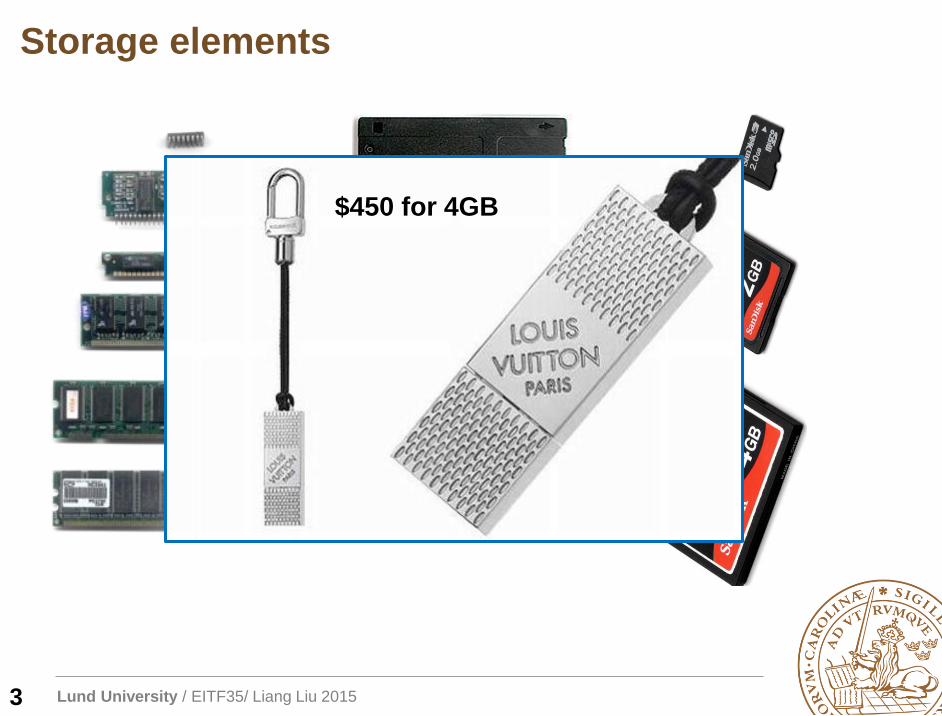
Storage elements
3
$450 for 4GB
Lund University / EITF35/ Liang Liu 2015
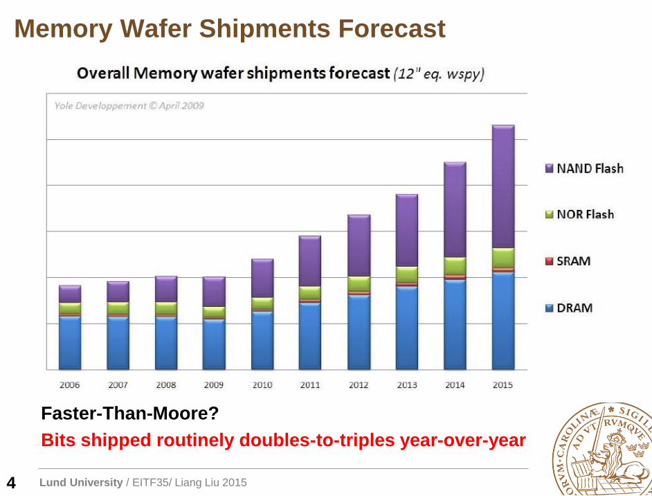
Memory Wafer Shipments Forecast
4
Faster-Than-Moore?
Bits shipped routinely doubles-to-triples year-over-year
Lund University / EITF35/ Liang Liu 2015
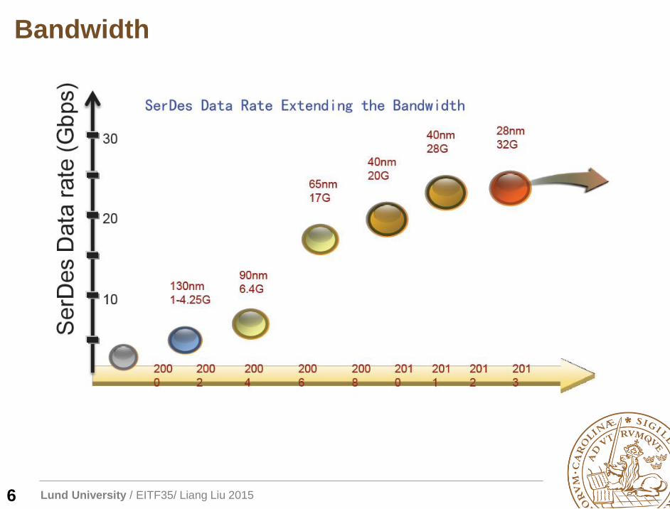
Bandwidth
6
Lund University / EITF35/ Liang Liu 20157
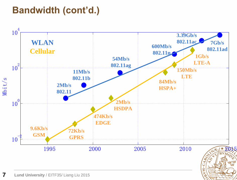
Bandwidth (cont’d.)
1995 2000 2005 2010 2015
10-2
100
102
104
Mbit/s
2Mb/s
802.11
11Mb/s
802.11b
54Mb/s
802.11ag
600Mb/s
802.11n
3.39Gb/s
802.11ac 7Gb/s
802.11ad
9.6Kb/s
GSM72Kb/s
GPRS
474Kb/s
EDGE
2Mb/s
HSDPA
84Mb/s
HSPA+
150Mb/s
LTE
1Gb/s
LTE-A
WLAN
Cellular
Lund University / EITF35/ Liang Liu 20158
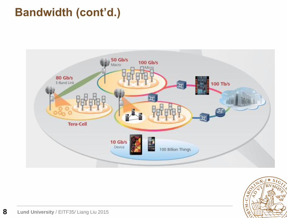
Bandwidth (cont’d.)
Lund University / EITF35/ Liang Liu 20159
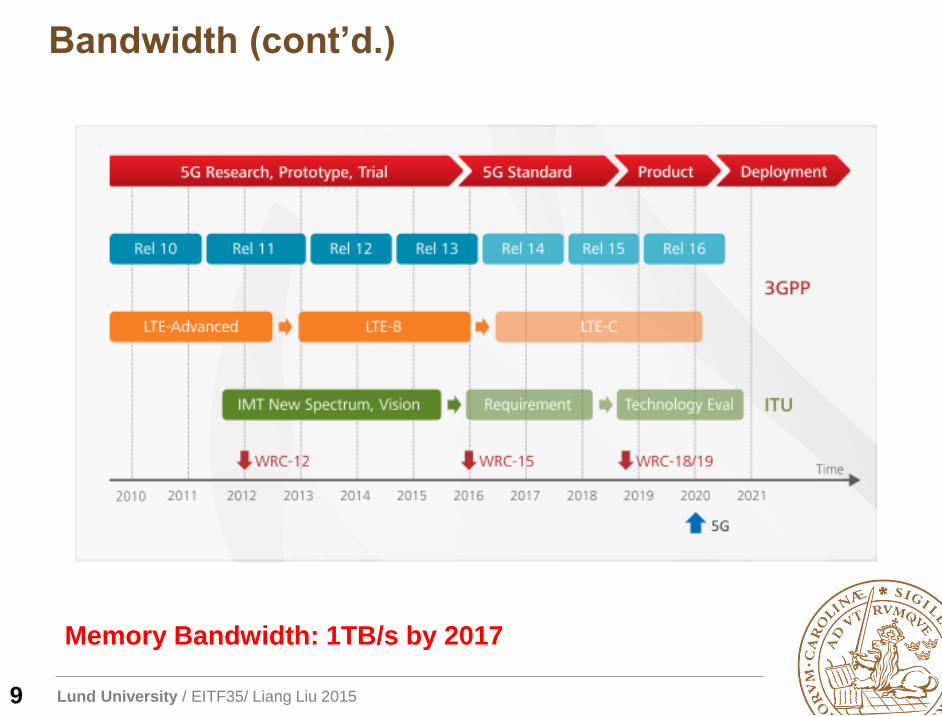
Bandwidth (cont’d.)
Memory Bandwidth: 1TB/s by 2017
Lund University / EITF35/ Liang Liu 2015
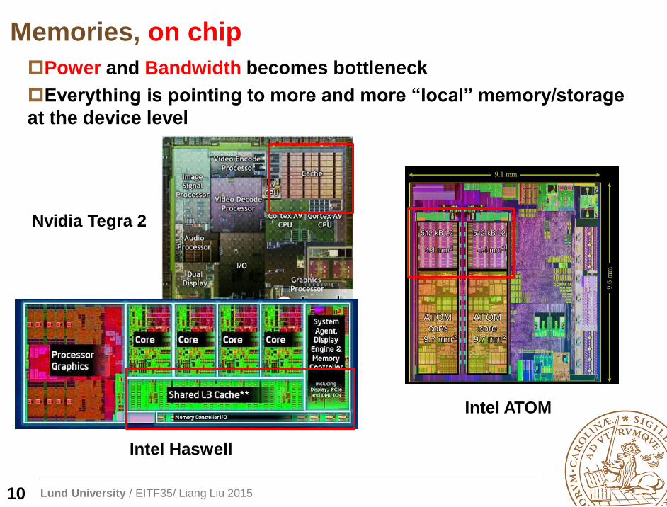
Memories, on chip
10
Power and Bandwidth becomes bottleneck
Everything is pointing to more and more “local” memory/storage
at the device level
Intel Haswell
Intel ATOM
Nvidia Tegra 2
Lund University / EITF35/ Liang Liu 2015
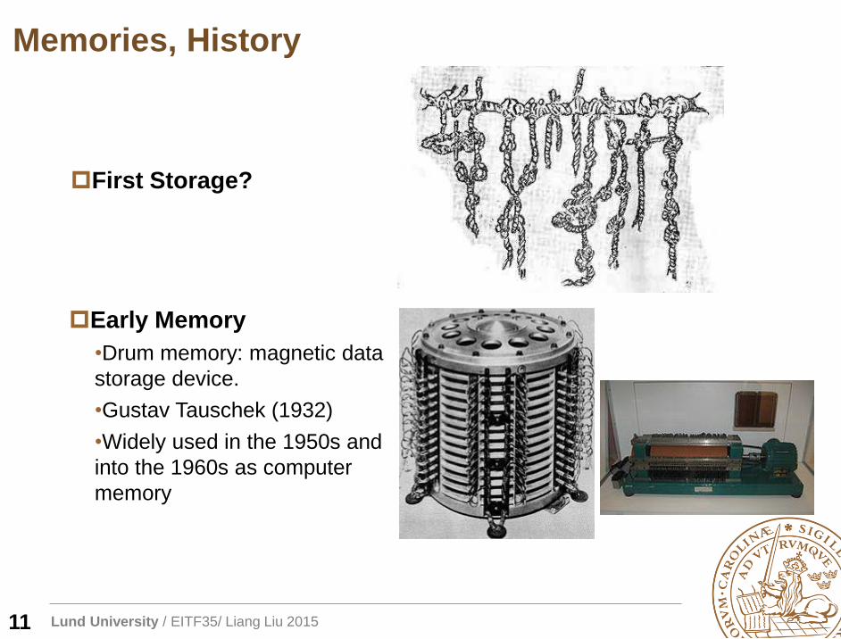
Memories, History
11
First Storage?
Early Memory
•Drum memory: magnetic data
storage device.
•Gustav Tauschek (1932)
•Widely used in the 1950s and
into the 1960s as computer
memory
Lund University / EITF35/ Liang Liu 2015
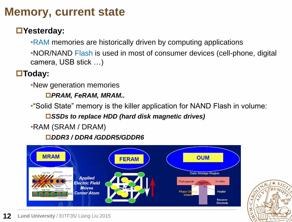
Memory, current state
12
Yesterday:
•RAM memories are historically driven by computing applications
•NOR/NAND Flash is used in most of consumer devices (cell-phone, digital
camera, USB stick …)
Today:
•New generation memories
PRAM, FeRAM, MRAM..
•“Solid State” memory is the killer application for NAND Flash in volume:
SSDs to replace HDD (hard disk magnetic drives)
•RAM (SRAM / DRAM)
DDR3 / DDR4 /GDDR5/GDDR6
Lund University / EITF35/ Liang Liu 2015
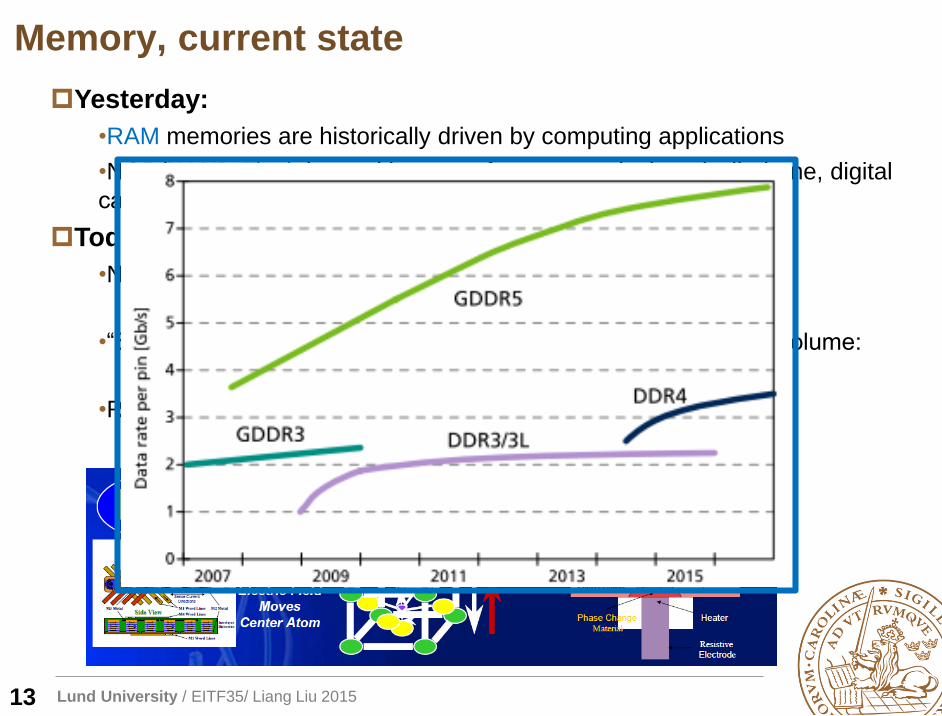
Memory, current state
13
Yesterday:
•RAM memories are historically driven by computing applications
•NOR/NAND Flash is used in most of consumer devices (cell-phone, digital
camera, USB stick …)
Today:
•New generation memories
PRAM, FeRAM, MRAM..
•“Solid State” memory is the killer application for NAND Flash in volume:
SSDs to replace HDD (hard disk magnetic drives)
•RAM (SRAM / DRAM)
DDR3 / DDR4 /GDDR5/GDDR6
Lund University / EITF35/ Liang Liu 2015
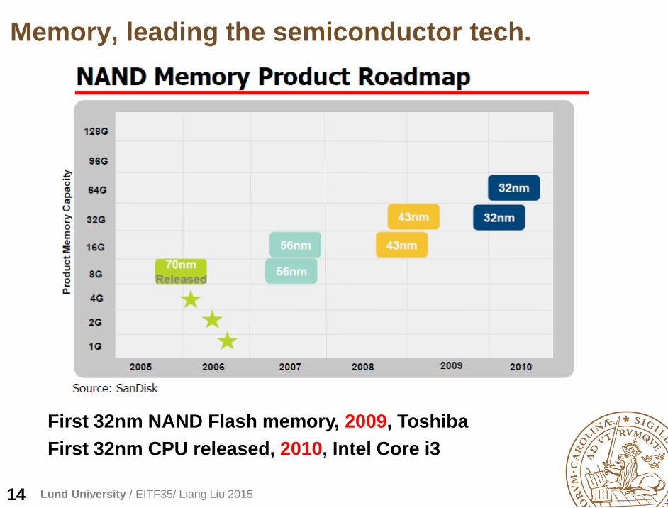
Memory, leading the semiconductor tech.
14
First 32nm NAND Flash memory, 2009, Toshiba
First 32nm CPU released, 2010, Intel Core i3
Lund University / EITF35/ Liang Liu 2015
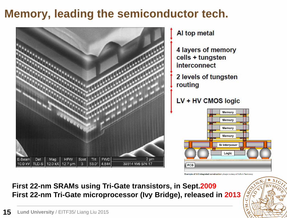
Memory, leading the semiconductor tech.
15
First 22-nm SRAMs using Tri-Gate transistors, in Sept.2009
First 22-nm Tri-Gate microprocessor (Ivy Bridge), released in 2013
Lund University / EITF35/ Liang Liu 2015
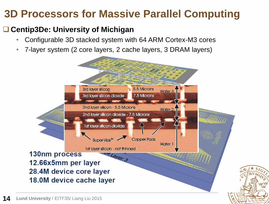
3D Processors for Massive Parallel Computing
Centip3De: University of Michigan
• Configurable 3D stacked system with 64 ARM Cortex-M3 cores
• 7-layer system (2 core layers, 2 cache layers, 3 DRAM layers)
14
Lund University / EITF35/ Liang Liu 2015
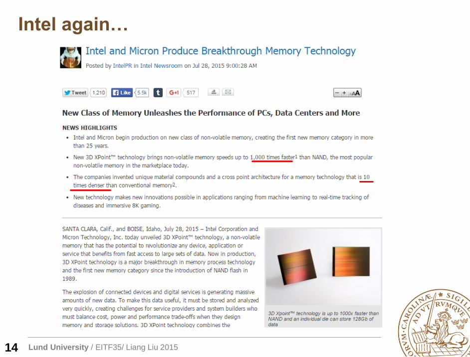
Intel again…
14
Lund University / EITF35/ Liang Liu 2015
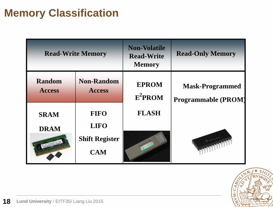
Read-Write MemoryNon-Volatile
Read-Write
Memory
Read-Only Memory
EPROM
E2PROM
FLASH
Random
Access
Non-Random
Access
SRAM
DRAM
Mask-Programmed
Programmable (PROM)
FIFO
Shift Register
CAM
LIFO
Memory Classification
18
Lund University / EITF35/ Liang Liu 2015
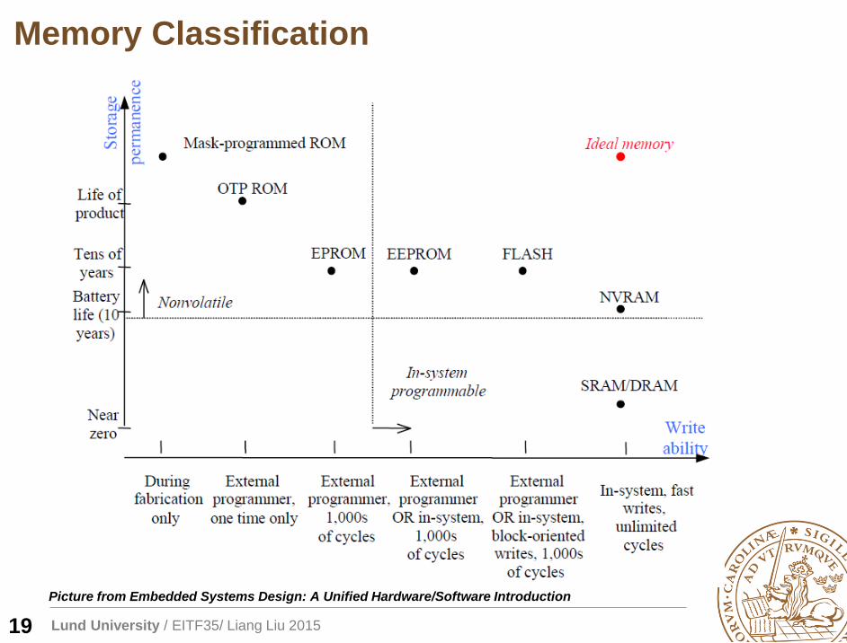
Memory Classification
Picture from Embedded Systems Design: A Unified Hardware/Software Introduction
19
Lund University / EITF35/ Liang Liu 2015
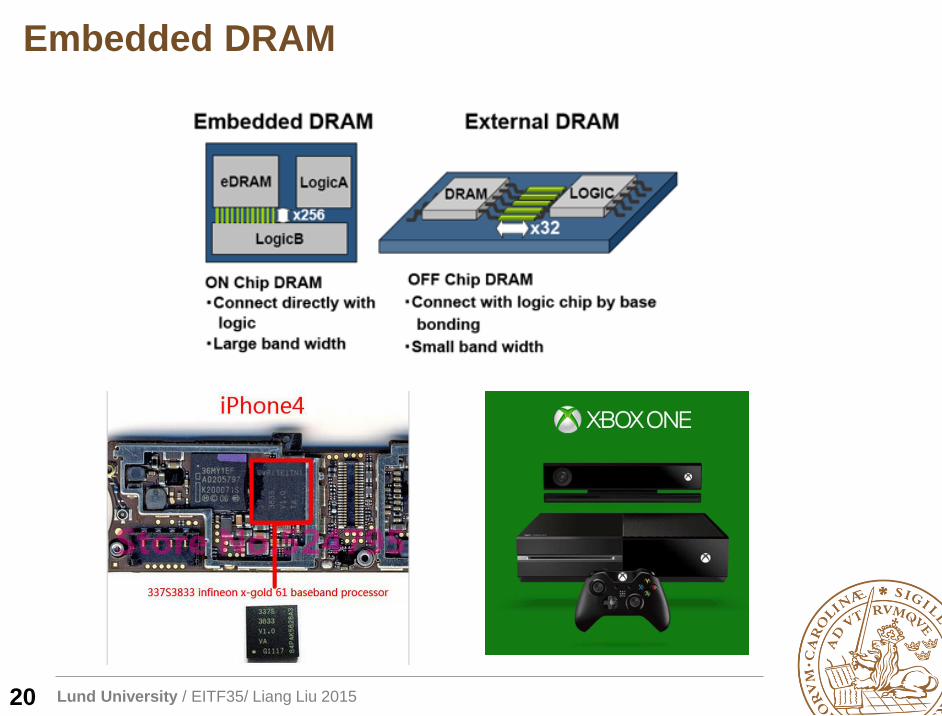
Embedded DRAM
20
Lund University / EITF35/ Liang Liu 2015
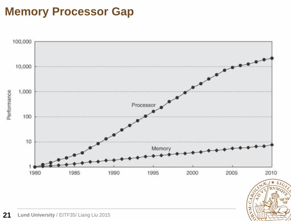
Memory Processor Gap
21
Lund University / EITF35/ Liang Liu 2015
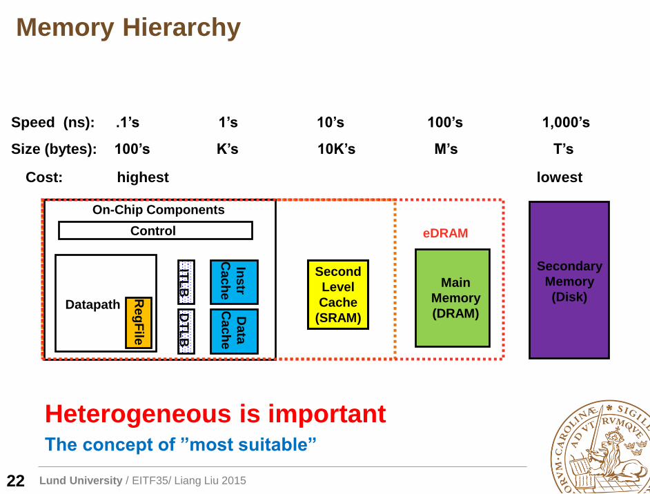
Memory Hierarchy
Second
Level
Cache
(SRAM)
Control
Datapath
Secondary
Memory
(Disk)
On-Chip Components
Re
gF
ile
Main
Memory
(DRAM)Da
ta
Ca
ch
eIn
str
Ca
ch
e
ITL
BD
TL
B
eDRAM
Speed (ns): .1’s 1’s 10’s 100’s 1,000’s
Size (bytes): 100’s K’s 10K’s M’s T’s
Cost: highest lowest
22
Heterogeneous is importantThe concept of ”most suitable”
Lund University / EITF35/ Liang Liu 2015
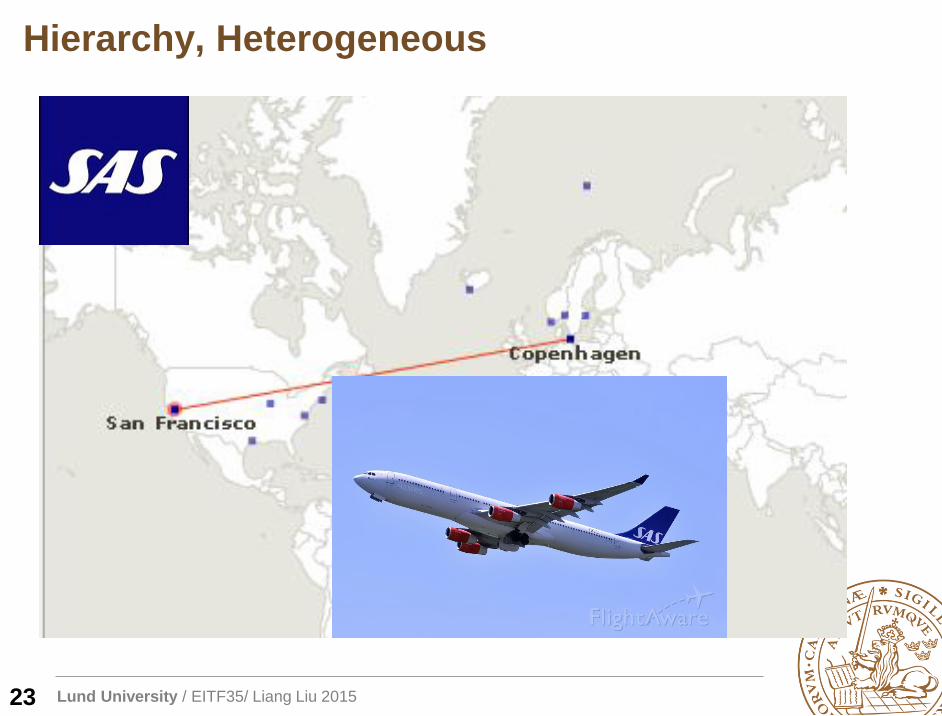
Hierarchy, Heterogeneous
23
Lund University / EITF35/ Liang Liu 2015
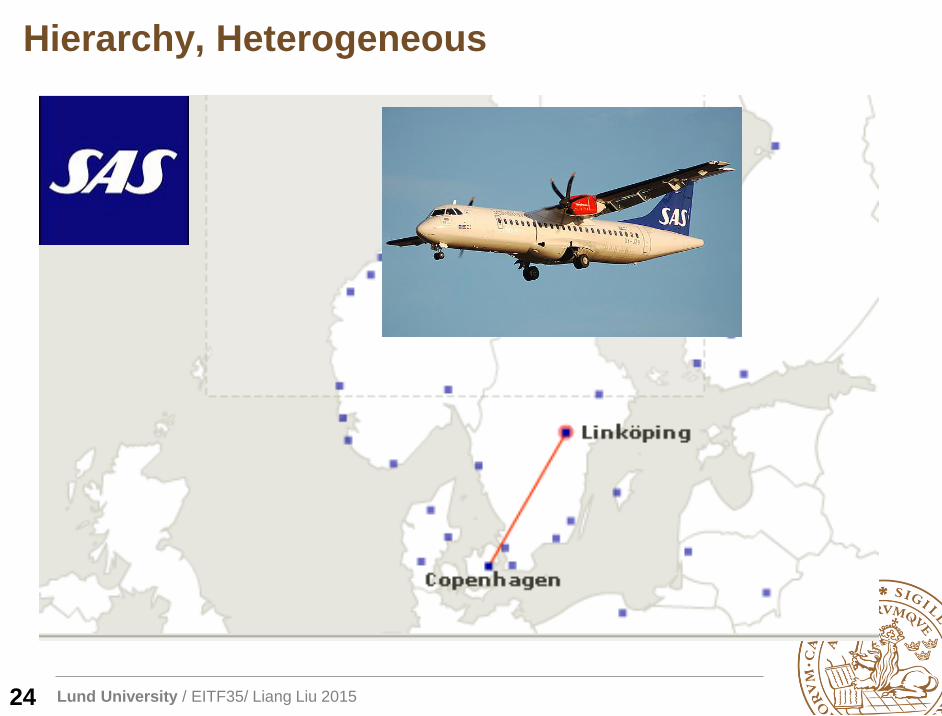
Hierarchy, Heterogeneous
24
Lund University / EITF35/ Liang Liu 2015
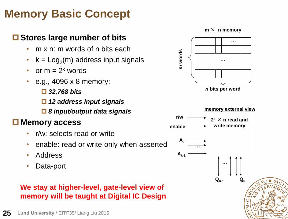
Memory Basic Concept
25
m × n memory
…
…
n bits per word
mw
ord
s
enable
2k× n read and
write memory
A0
…
r/w
…
Q0Qn-1
Ak-1
memory external view
Stores large number of bits
• m x n: m words of n bits each
• k = Log2(m) address input signals
• or m = 2k words
• e.g., 4096 x 8 memory:
32,768 bits
12 address input signals
8 input/output data signals
Memory access
• r/w: selects read or write
• enable: read or write only when asserted
• Address
• Data-port
We stay at higher-level, gate-level view of
memory will be taught at Digital IC Design
Lund University / EITF35/ Liang Liu 2015
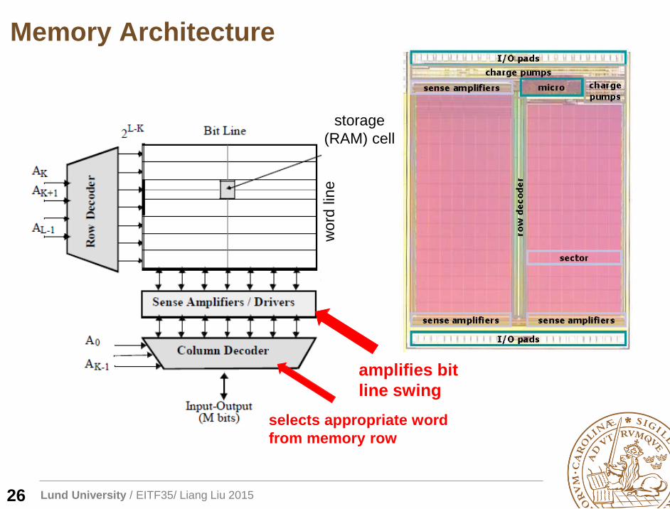
Memory Architecture
26
word
lin
e
storage
(RAM) cell
selects appropriate word
from memory row
amplifies bit
line swing
Lund University / EITF35/ Liang Liu 2015
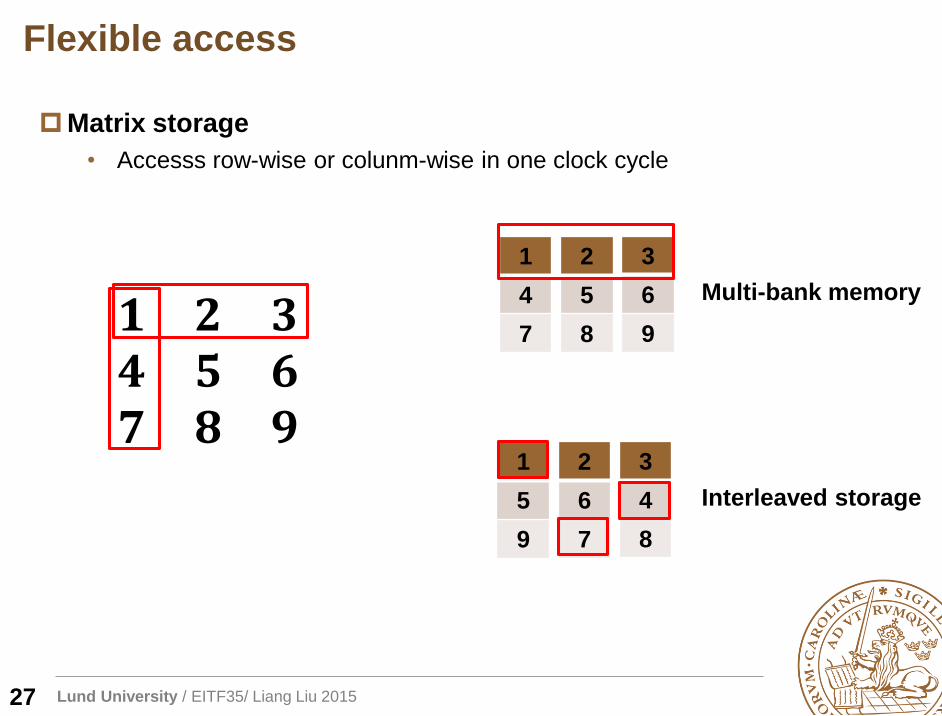
Flexible access
27
𝟏 𝟐 𝟑𝟒 𝟓 𝟔𝟕 𝟖 𝟗
Matrix storage
• Accesss row-wise or colunm-wise in one clock cycle
1
4
7
2
5
8
3
6
9
Multi-bank memory
1
5
9
2
6
7
3
4
8
Interleaved storage
Lund University / EITF35/ Liang Liu 2015
Outline
Overview of Memory
•Application, history, trend
•Different memory type
•Overall architecture
Registers as Storage Element
•Register File
•FIFO
Xilinx Storage Elements
28
Lund University / EITF35/ Liang Liu 2015
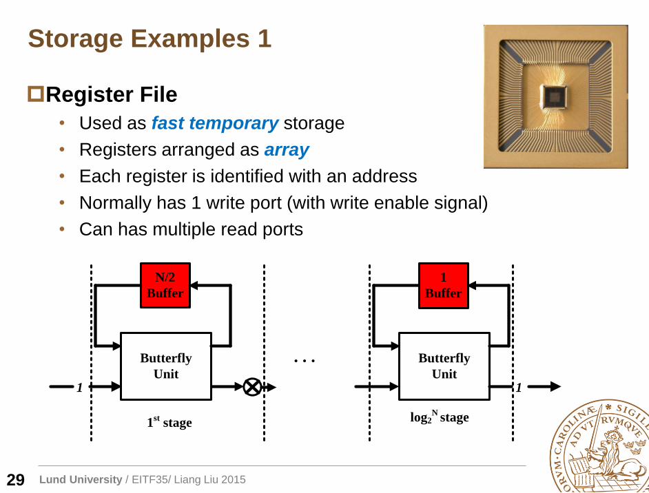
Storage Examples 1
Register File
• Used as fast temporary storage
• Registers arranged as array
• Each register is identified with an address
• Normally has 1 write port (with write enable signal)
• Can has multiple read ports
29
Butterfly
Unit
1st stage log2
N stage
1
N/2
Buffer
. . . Butterfly
Unit
1
Buffer
1
Lund University / EITF35/ Liang Liu 2015
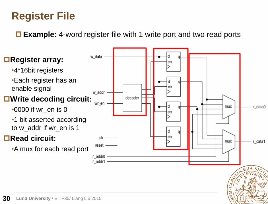
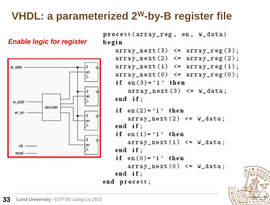
Register File
Example: 4-word register file with 1 write port and two read ports
30
Register array:
•4*16bit registers
•Each register has an
enable signal
Write decoding circuit:
•0000 if wr_en is 0
•1 bit asserted according
to w_addr if wr_en is 1
Read circuit:
•A mux for each read port
Lund University / EITF35/ Liang Liu 2015
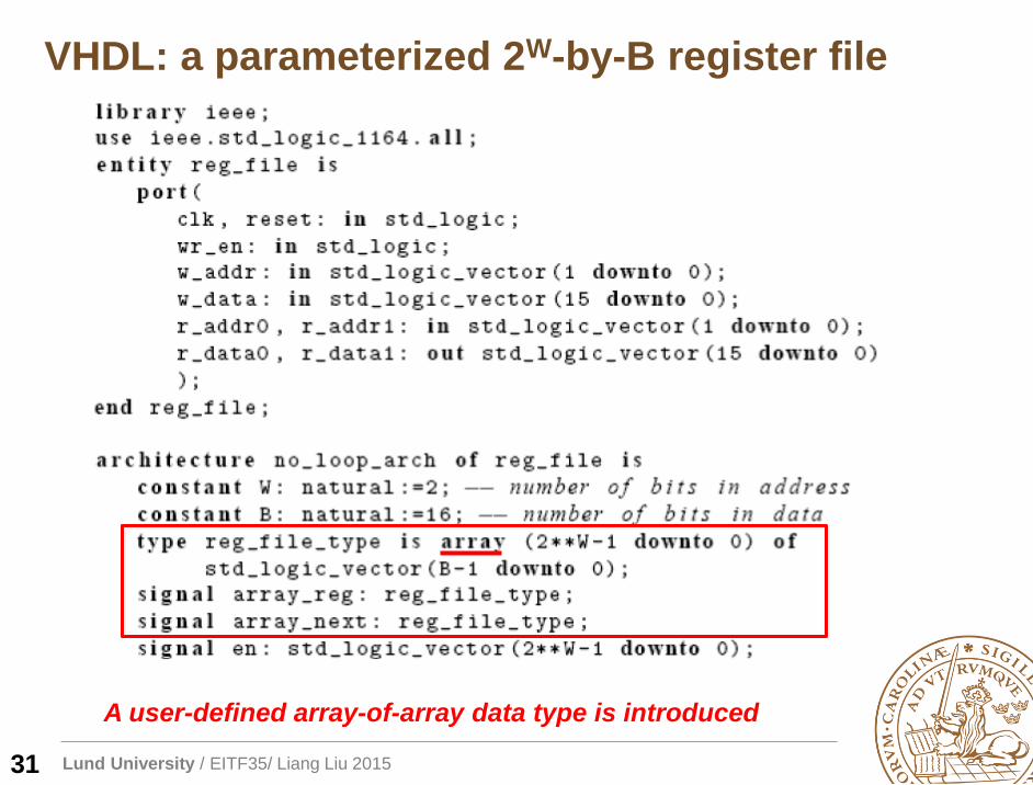
VHDL: a parameterized 2W-by-B register file
31
A user-defined array-of-array data type is introduced
Lund University / EITF35/ Liang Liu 2015
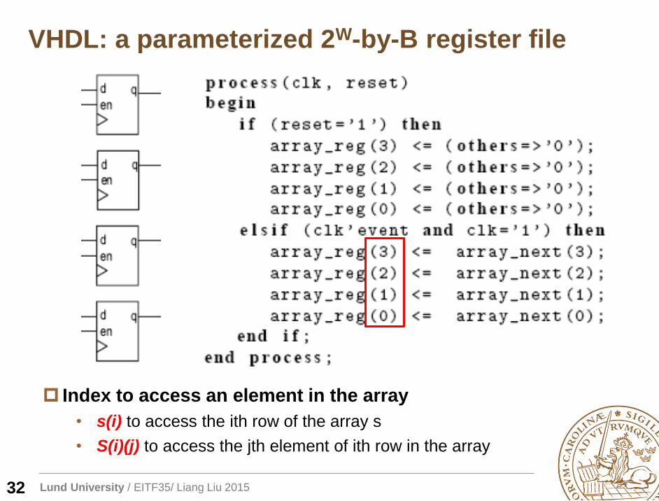
VHDL: a parameterized 2W-by-B register file
32
Index to access an element in the array
• s(i) to access the ith row of the array s
• S(i)(j) to access the jth element of ith row in the array
Lund University / EITF35/ Liang Liu 2015
VHDL: a parameterized 2W-by-B register file
33
Enable logic for register
Lund University / EITF35/ Liang Liu 2015
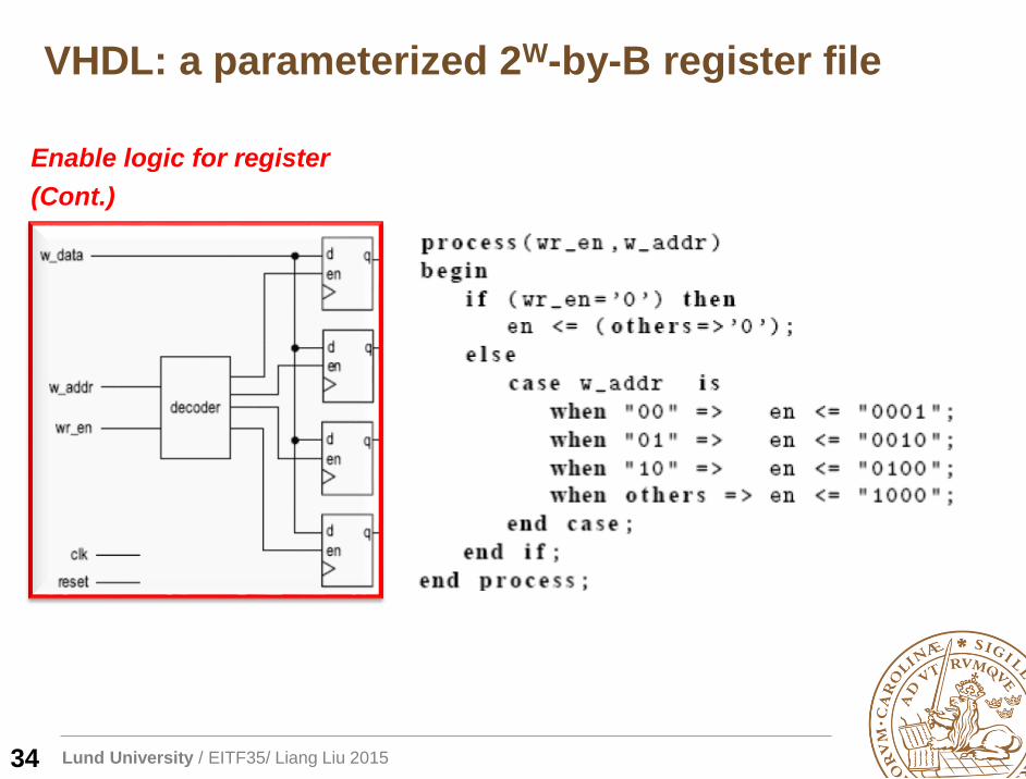
VHDL: a parameterized 2W-by-B register file
34
Enable logic for register
(Cont.)
Lund University / EITF35/ Liang Liu 2015
VHDL: a parameterized 2W-by-B register file
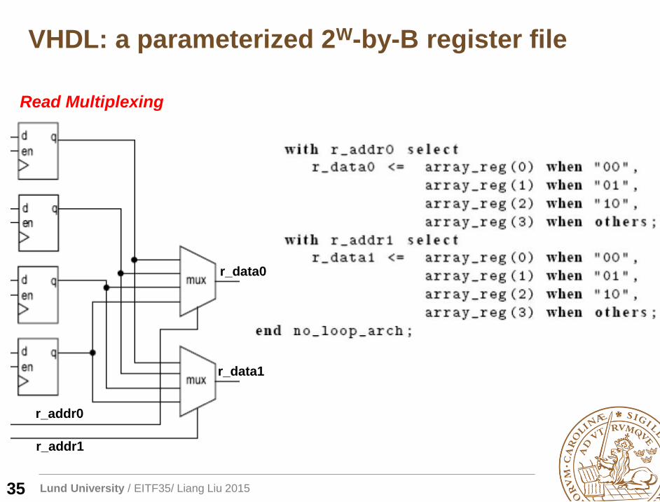
35
Read Multiplexing
r_data0
r_data1
r_addr0
r_addr1
Lund University / EITF35/ Liang Liu 2015
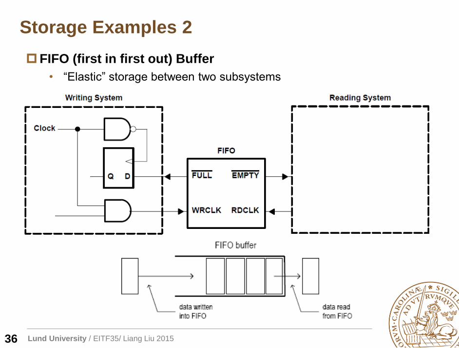
Storage Examples 2
FIFO (first in first out) Buffer
• “Elastic” storage between two subsystems
36
Lund University / EITF35/ Liang Liu 2015
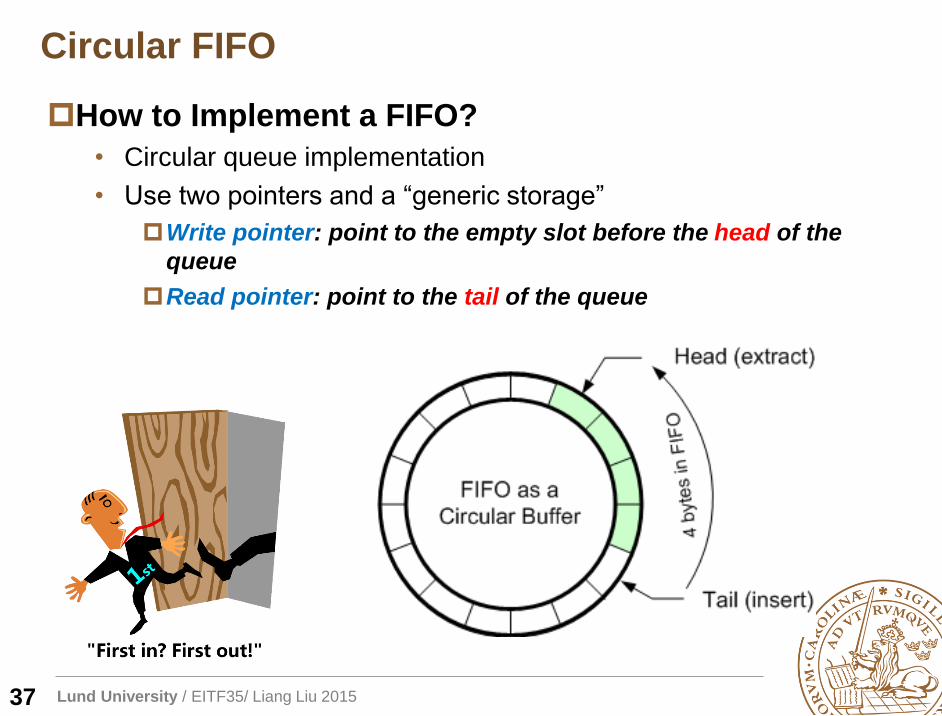
Circular FIFO
How to Implement a FIFO?
• Circular queue implementation
• Use two pointers and a “generic storage”
Write pointer: point to the empty slot before the head of the
queue
Read pointer: point to the tail of the queue
37
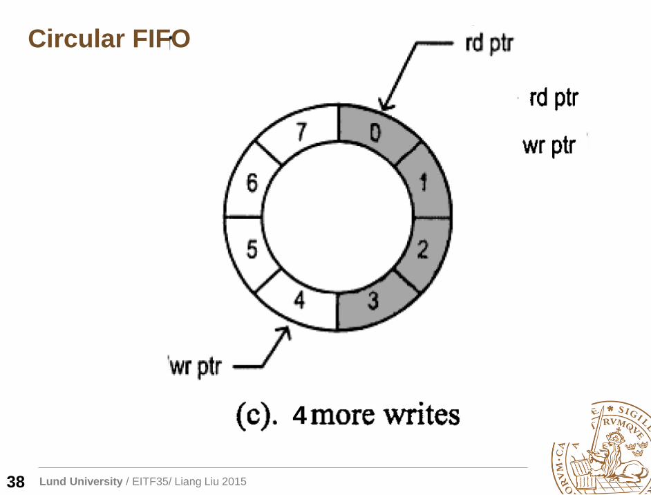
Lund University / EITF35/ Liang Liu 201538
(f) 5 6 4
Circular FIFO
Lund University / EITF35/ Liang Liu 2015
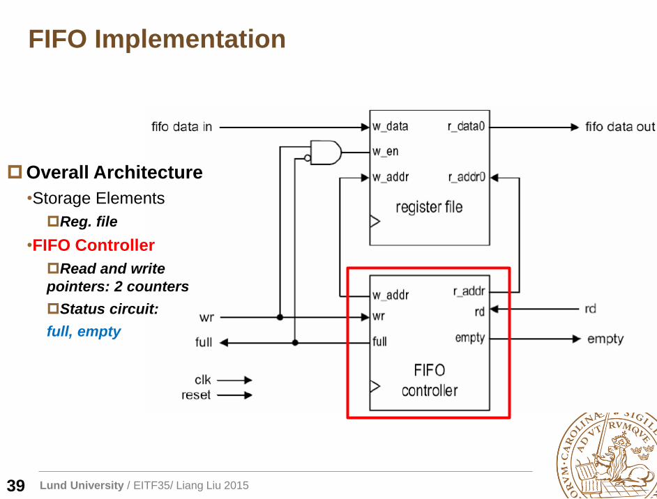
FIFO Implementation
Overall Architecture
•Storage Elements
Reg. file
•FIFO Controller
Read and write
pointers: 2 counters
Status circuit:
full, empty
39
Lund University / EITF35/ Liang Liu 2015
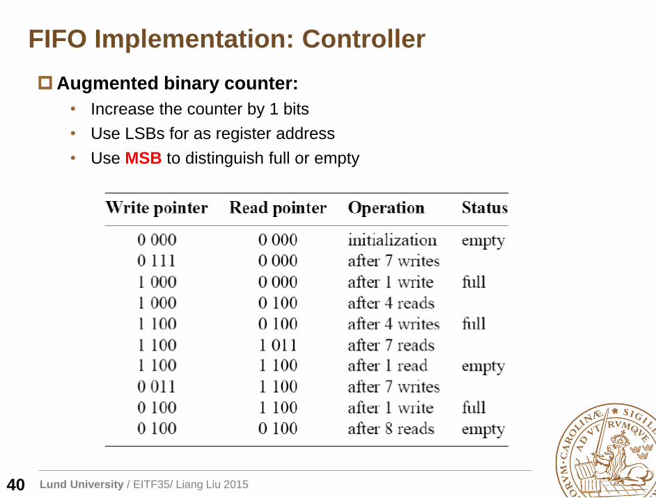
FIFO Implementation: Controller
Augmented binary counter:
• Increase the counter by 1 bits
• Use LSBs for as register address
• Use MSB to distinguish full or empty
40
Lund University / EITF35/ Liang Liu 2015
Outline
Overview of Memory
•Application, history, trend
•Different memory type
•Overall architecture
Registers as Storage Element
•Register File
•FIFO
Xilinx Storage Elements
Memory Generator
41
Lund University / EITF35/ Liang Liu 2015
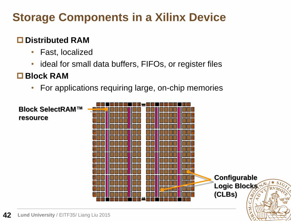
Storage Components in a Xilinx Device
Distributed RAM
• Fast, localized
• ideal for small data buffers, FIFOs, or register files
Block RAM
• For applications requiring large, on-chip memories
42
Configurable
Logic Blocks
(CLBs)
Block SelectRAM™
resource
Lund University / EITF35/ Liang Liu 2015
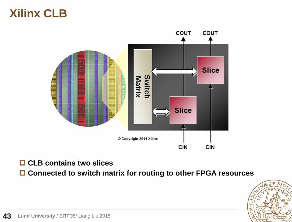
Xilinx CLB
CLB contains two slices
Connected to switch matrix for routing to other FPGA resources
43
Sw
itch
Matrix
CIN CIN
COUT COUT
Lund University / EITF35/ Liang Liu 2015
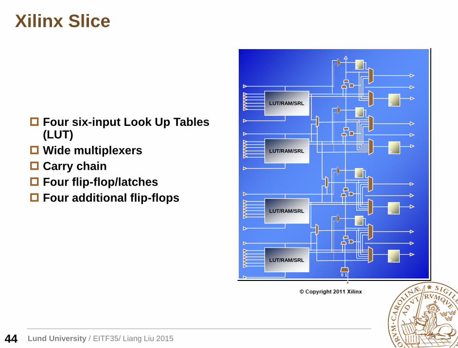
Xilinx Slice
Four six-input Look Up Tables (LUT)
Wide multiplexers
Carry chain
Four flip-flop/latches
Four additional flip-flops
44
LUT/RAM/SRL
LUT/RAM/SRL
LUT/RAM/SRL
LUT/RAM/SRL
0 1
Lund University / EITF35/ Liang Liu 2015
Two type of slice
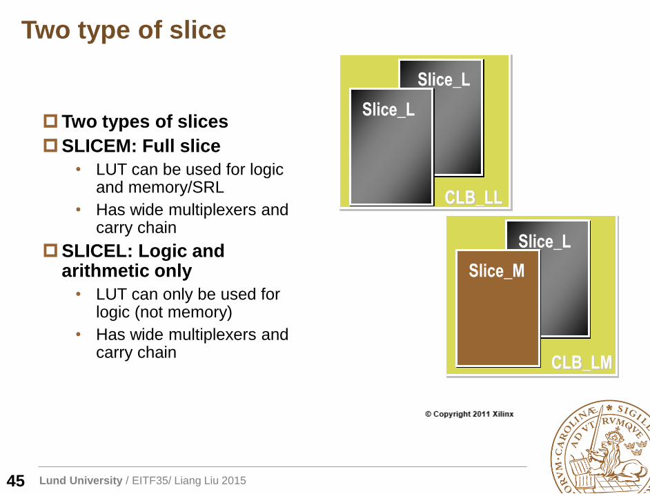
Two types of slices
SLICEM: Full slice
• LUT can be used for logic and memory/SRL
• Has wide multiplexers and carry chain
SLICEL: Logic and arithmetic only
• LUT can only be used for logic (not memory)
• Has wide multiplexers and carry chain
45
CLB_LL
Slice_L
Slice_L
CLB_LM
Slice_L
Slice_M
Lund University / EITF35/ Liang Liu 2015
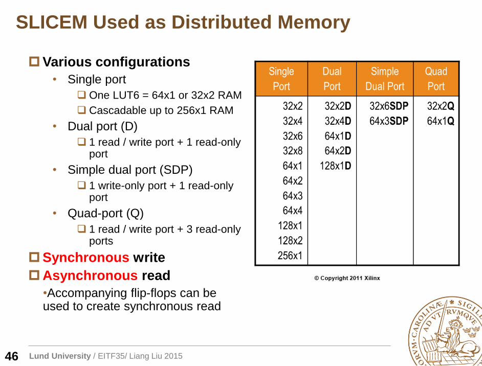
Various configurations
• Single port
One LUT6 = 64x1 or 32x2 RAM
Cascadable up to 256x1 RAM
• Dual port (D)
1 read / write port + 1 read-only port
• Simple dual port (SDP)
1 write-only port + 1 read-only port
• Quad-port (Q)
1 read / write port + 3 read-only ports
Synchronous write
Asynchronous read
•Accompanying flip-flops can be used to create synchronous read
SLICEM Used as Distributed Memory
46
Lund University / EITF35/ Liang Liu 2015
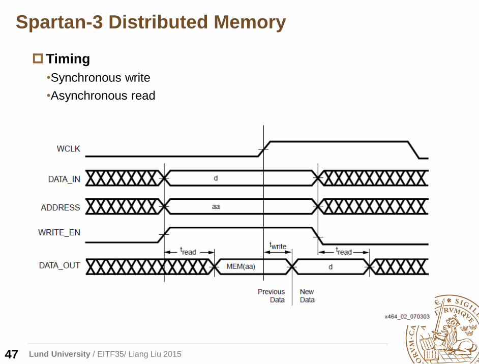
Timing
•Synchronous write
•Asynchronous read
Spartan-3 Distributed Memory
47
Lund University / EITF35/ Liang Liu 2015
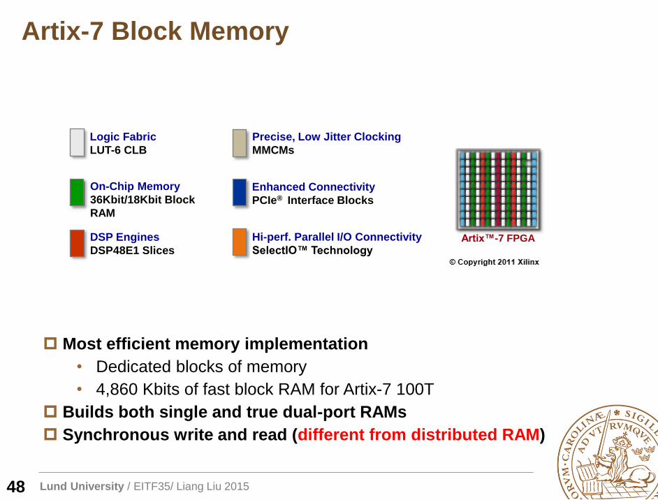
Artix-7 Block Memory
48
Most efficient memory implementation
• Dedicated blocks of memory
• 4,860 Kbits of fast block RAM for Artix-7 100T
Builds both single and true dual-port RAMs
Synchronous write and read (different from distributed RAM)
Artix™-7 FPGA
Precise, Low Jitter Clocking
MMCMs
Logic Fabric
LUT-6 CLB
DSP Engines
DSP48E1 Slices
On-Chip Memory
36Kbit/18Kbit Block
RAM
Enhanced Connectivity
PCIe® Interface Blocks
Hi-perf. Parallel I/O Connectivity
SelectIO™ Technology
Lund University / EITF35/ Liang Liu 2015
Artix-7 Block Memory
49
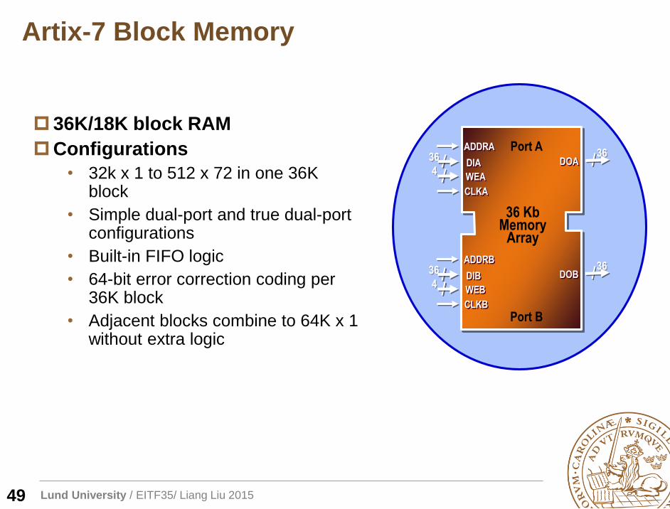
36K/18K block RAM
Configurations
• 32k x 1 to 512 x 72 in one 36K block
• Simple dual-port and true dual-port configurations
• Built-in FIFO logic
• 64-bit error correction coding per 36K block
• Adjacent blocks combine to 64K x 1 without extra logic
36DIA
ADDRA36
DOA
Port A
36 KbMemory
Array
CLKA
WEA4
36DIB
ADDRB36
DOB
Port BCLKB
WEB4
Lund University / EITF35/ Liang Liu 2015
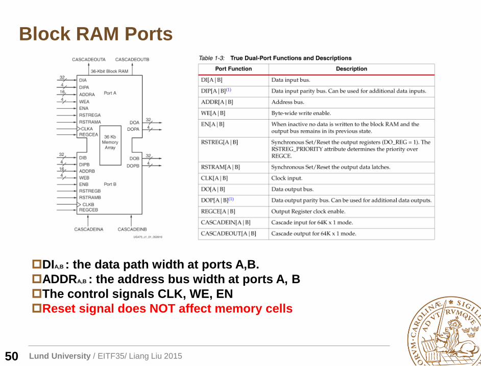
Block RAM Ports
DIA,B : the data path width at ports A,B.
ADDRA,B : the address bus width at ports A, B
The control signals CLK, WE, EN
Reset signal does NOT affect memory cells
50
Lund University / EITF35/ Liang Liu 2015
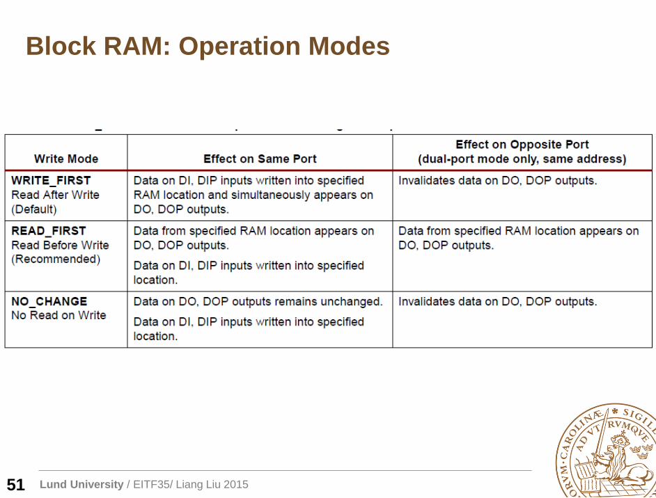
Block RAM: Operation Modes
51
Lund University / EITF35/ Liang Liu 2015
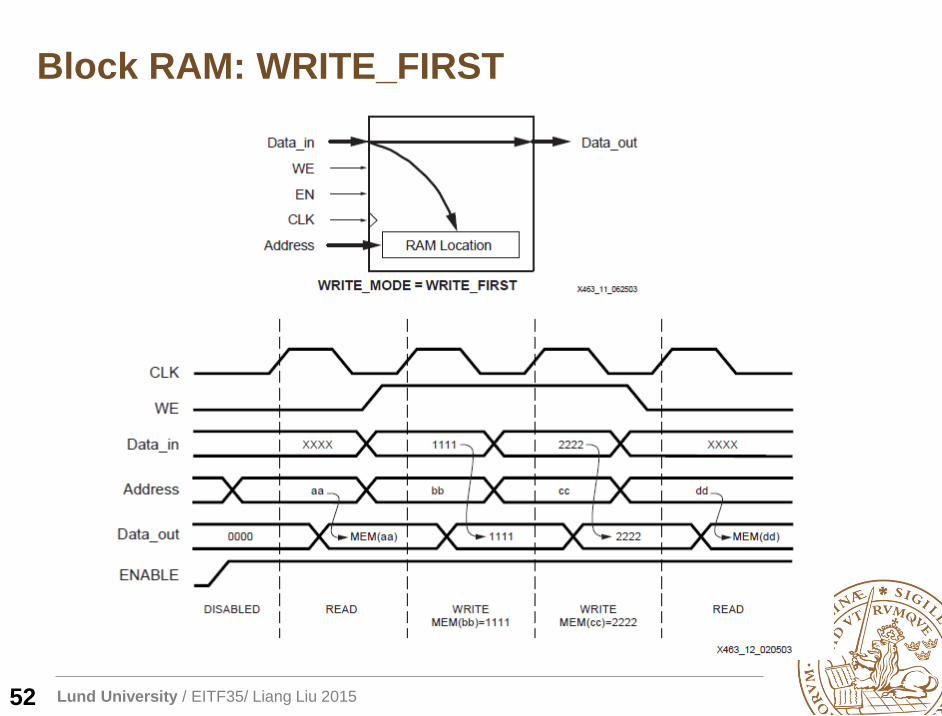
Block RAM: WRITE_FIRST
52
Lund University / EITF35/ Liang Liu 2015
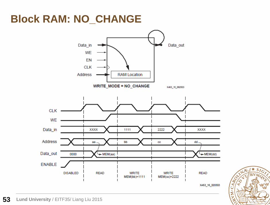
Block RAM: NO_CHANGE
53
Lund University / EITF35/ Liang Liu 2015
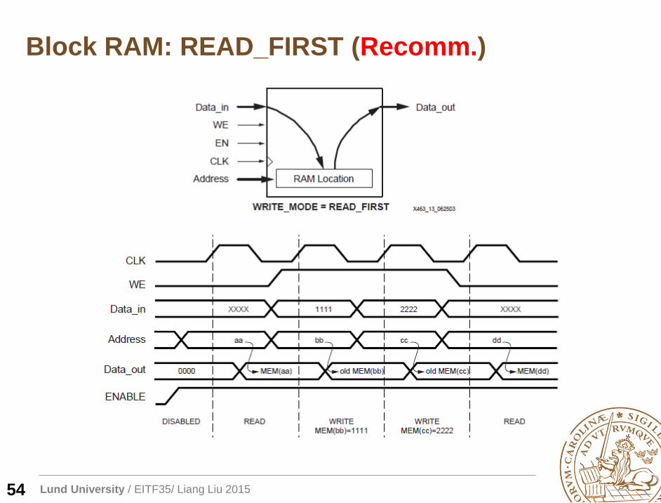
Block RAM: READ_FIRST (Recomm.)
54
Lund University / EITF35/ Liang Liu 2015
Reading Advice
RTL Hardware Design Using VHDL: P276-P292
UG437 7 Series FPGAs Memory Resources
UG901 Vivado Design Suite User Guide Synthesis
55


