Page 1
Doctoral School in Information Technologies
XXX Cycle
Electrical Measurements and Numerical Simulations of Ion
Implanted 4H-SiC PiN diodes
Coordinator:
Chiar.mo Prof. Marco Locatelli
Tutor:
Prof.ssa Giovanna Sozzi
Co–Tutor:
Dott.ssa Roberta Nipoti
Ph.D student:Maurizio Puzzanghera
Anni 2014/2017
Page 3
To my family . . .
Page 5
Table of Contents
Introduction 1
1 Single Crystal Silicon Carbide 5
1.1 Material Properties . . . . . . . . . . . . . . . . . . . . . . . . . . 5
1.2 SiC Wafers . . . . . . . . . . . . . . . . . . . . . . . . . . . . . . 7
1.2.1 Early history . . . . . . . . . . . . . . . . . . . . . . . . . 7
1.2.2 SiC Epitaxial Growth . . . . . . . . . . . . . . . . . . . . . 10
1.3 Technological improvements in SiC Growth substrates . .. . . . . 12
2 Ion Implanted vertical 4H-SiC PiN diodes 15
2.1 Ion Implantation . . . . . . . . . . . . . . . . . . . . . . . . . . . . 15
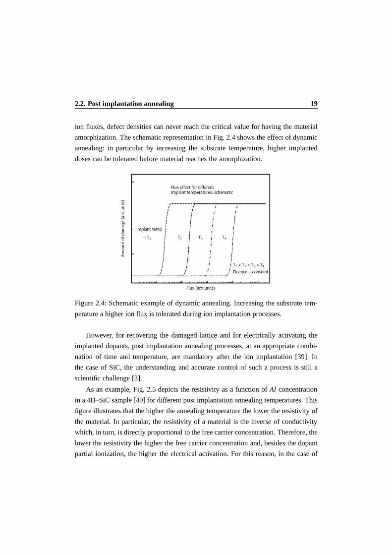
2.2 Post implantation annealing . . . . . . . . . . . . . . . . . . . . . . 18
2.3 Ohmic Contacts . . . . . . . . . . . . . . . . . . . . . . . . . . . . 21
2.4 Process steps . . . . . . . . . . . . . . . . . . . . . . . . . . . . . 24
2.5 Static electrical measurements . . . . . . . . . . . . . . . . . . . .25
2.5.1 Device schematic cross–sections and selection criteria . . . 25
2.5.2 Experimental Setup description . . . . . . . . . . . . . . . 25
2.5.3 Diode selection criteria . . . . . . . . . . . . . . . . . . . . 27
2.5.4 Experimental measurements . . . . . . . . . . . . . . . . . 28
3 Analysis of Static current–voltage curves 33
3.1 Motivations . . . . . . . . . . . . . . . . . . . . . . . . . . . . . . 33
3.2 Extraction of Area and Periphery current densities . . . .. . . . . . 34
Page 6
ii Table of Contents
3.2.1 Theoretical background I . . . . . . . . . . . . . . . . . . . 34
3.2.2 Experimental Area and Perimeter current density curves . . 37
3.3 Current temperature dependences and Arrhenius plot . . .. . . . . 43
3.3.1 Theoretical background II . . . . . . . . . . . . . . . . . . 43
3.3.2 Calculated constant values . . . . . . . . . . . . . . . . . . 48
3.3.3 Data analysis and experimental results . . . . . . . . . . . .49
3.4 Numerical simulations . . . . . . . . . . . . . . . . . . . . . . . . 57
3.4.1 Motivations . . . . . . . . . . . . . . . . . . . . . . . . . . 57
3.4.2 Used models and simulation parameters . . . . . . . . . . . 58
3.4.3 Simulation results . . . . . . . . . . . . . . . . . . . . . . 59
4 Lifetime measurements in SiC devices 69
4.1 Motivations . . . . . . . . . . . . . . . . . . . . . . . . . . . . . . 69
4.2 Lifetime definition . . . . . . . . . . . . . . . . . . . . . . . . . . 69
4.2.1 Recombination lifetime . . . . . . . . . . . . . . . . . . . . 70
4.2.2 Generation lifetime . . . . . . . . . . . . . . . . . . . . . . 71
4.2.3 Continuity equation for Generation/Recombination processes 72
4.2.4 Surface recombination velocity and surface recombination
lifetime . . . . . . . . . . . . . . . . . . . . . . . . . . . . 73
4.3 Lifetime measurements . . . . . . . . . . . . . . . . . . . . . . . . 73
4.3.1 Open Circuit Voltage Decay . . . . . . . . . . . . . . . . . 74
4.3.2 Experimental setup . . . . . . . . . . . . . . . . . . . . . . 75
4.3.3 Experimental set–up characterization . . . . . . . . . . . .77
4.3.4 Measured devices . . . . . . . . . . . . . . . . . . . . . . . 82
4.3.5 OCVD measurements and ambipolar lifetime extraction. . 85
4.3.6 Volume and Surface lifetime . . . . . . . . . . . . . . . . . 93
Summary 99
Bibliography 103
Acknowledgements 115
Page 7
List of Figures
1.1 (a) Elementary structural unit of SiC material. (b) A second type ro-
tated of 180 around the stacking direction, with respect to (a). . . . 5
1.2 Table reporting the main physical properties of the mostused SiC
polytypes for electronic application. . . . . . . . . . . . . . . . . . 6
1.3 On the left 2.5cm 6H–SiC manufactured wafer by CREE by using
seeded sublimation technique, on the right single–crystalSiC sub-
strates available prior to 1989. . . . . . . . . . . . . . . . . . . . . 8
1.4 (a) Increase of wafer size demonstrated by CREE company.(b) Re-
duction of micropipes densities in SiC Substrates of different dimen-
sion. . . . . . . . . . . . . . . . . . . . . . . . . . . . . . . . . . . 9
1.5 List of single–crystal SiC wafer providers since early 1990s. . . . . 9
1.6 Schematic view of a step–controlled epitaxial growth. .. . . . . . . 11
1.7 Current knowledge status of SiC process technologies for electronic
grade substrates. . . . . . . . . . . . . . . . . . . . . . . . . . . . . 12
2.1 Illustration of tilt and twist angles for defining implantation geome-
try. See text for further details. . . . . . . . . . . . . . . . . . . . . 16
2.2 Depth profiles of Nitrogen implantation into SiC <0001> with vari-
ous tilt angles. . . . . . . . . . . . . . . . . . . . . . . . . . . . . . 17
2.3 Example of multiple ion implantetion processes to obtain a flat box
doping profile. . . . . . . . . . . . . . . . . . . . . . . . . . . . . . 18
Page 8
iv List of Figures
2.4 Schematic example of dynamic annealing. Increasing thesubstrate
temperature a higher ion flux is tolerated during ion implantation pro-
cesses. . . . . . . . . . . . . . . . . . . . . . . . . . . . . . . . . 19
2.5 Resistivity versus Aluminum implanted concentration in a 4H-SiC
sample for different annealing temperatures, see text for further details. 20
2.6 Surface morphology of SiC samples after annealing process (a) with-
out protective carbon cap and (b) with protective carbon cap. . . . . 21
2.7 Band diagram of 4H-SiC. . . . . . . . . . . . . . . . . . . . . . . . 22
2.8 (a) Ni deposition on n–type 6H-SiC (b) Al/Ti deposition on p–type
6H-SiC, before and after annealing process. . . . . . . . . . . . . .23
2.9 In the top a schematic cross section of the studied diodesand in the
bottom a processed chip containing the studied devices are shown. . 26
2.10 (a) Linear scale and (b) log scale current–voltage characteristic of a
400µm diameter diode of this study, for varying temperatures. . . .28
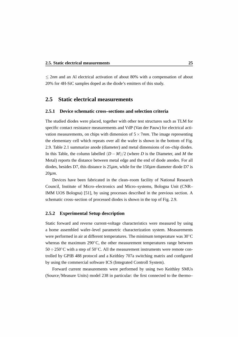
2.11 Trend of ideality factor of curves showed in Fig. 2.10. .. . . . . . . 30
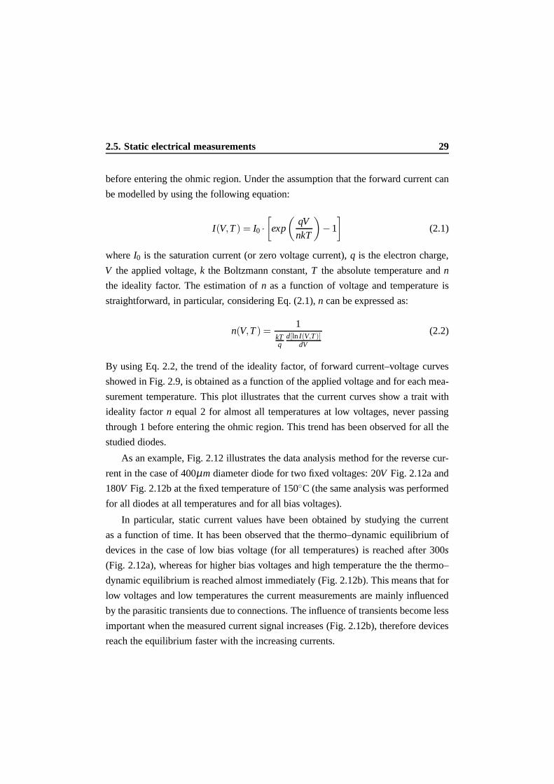
2.12 Example of data analysis for two different reverse biasvoltage (a)
20V and (b) 180V for the fixed temperature of 150C for a 400µm
diameter diode. . . . . . . . . . . . . . . . . . . . . . . . . . . . . 30
2.13 Typical reverse characteristic of a diode of this studyfor all the mea-
surement temperatures. . . . . . . . . . . . . . . . . . . . . . . . . 31
3.1 Two–dimensional schematic representation of the Sha model for diodes
of this study (see Chapter 2, Fig. 2.9). . . . . . . . . . . . . . . . . 37
3.2 (a) Current–voltage characteristics at RT for all diodes of this study.
(b) The curves showed in (a) are divided by the anode area for ob-
taining the corresponding current densities. . . . . . . . . . . .. . 38
3.3 Experimental current data divided by the emitter area ofthe studied
diodes and plotted versus the ratio 2/r by using Eq. (3.4) at 30C in
linear (a) and logarithmic scale (b). . . . . . . . . . . . . . . . . . . 38
3.4 Experimental perimeter (a) and area (b) current densities plotted ver-
sus the applied voltage for several temperatures. . . . . . . . .. . . 39
Page 9
List of Figures v
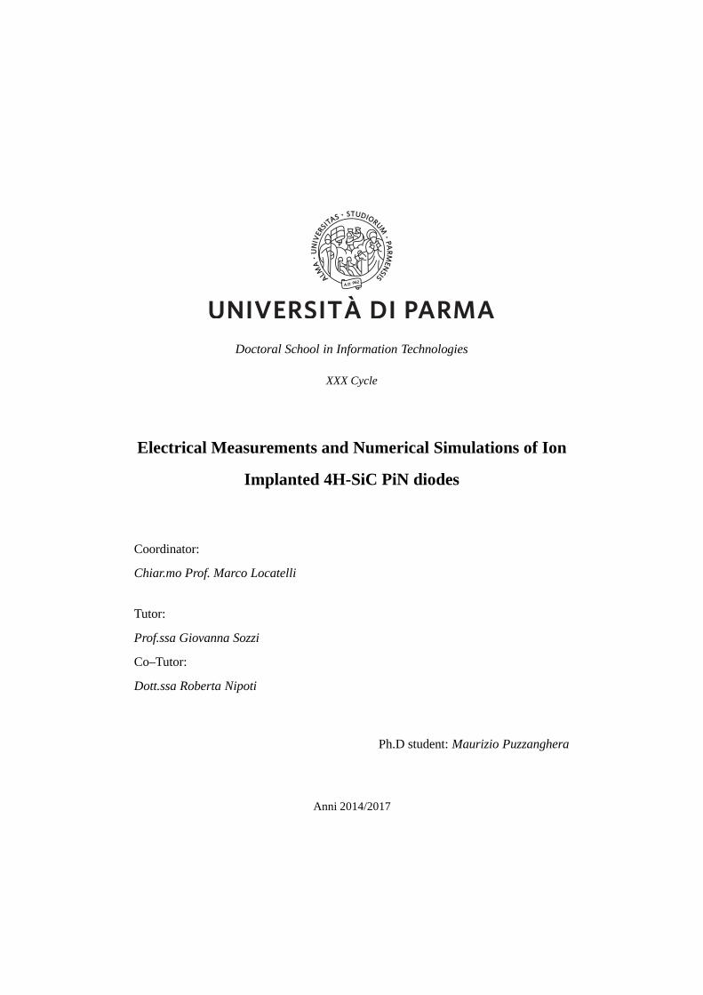
3.5 Trend of the ideality factorn for the perimeter (a) and the area (b)
current density. . . . . . . . . . . . . . . . . . . . . . . . . . . . . 40
3.6 (a) Reverse current–voltage curves at RT for all diodes of this study.
(b) The curves showed in (a) were divided to the anode area forob-
taining reverse current densities. . . . . . . . . . . . . . . . . . . . 41
3.7 (a) Perimeter (in linear scale) and (b) Area (in logarithmic scale) re-
verse current densities . . . . . . . . . . . . . . . . . . . . . . . . 42
3.8 Reverse area current density (JR,Vol) for increasing voltage and tem-
perature is shown. This current was obtained by using algorithm de-
scribed in the previous section, assuming negligible perimeter current
(null slope). . . . . . . . . . . . . . . . . . . . . . . . . . . . . . . 42
3.9 Example of dopants partial ionization at different temperatures in the
case of 6H–SiC material. . . . . . . . . . . . . . . . . . . . . . . . 48
3.10 Experimental hole density as a function of temperature. . . . . . . . 49
3.11 Area (black square) and perimeter (red circle) currentdensities at
250C. The dashed curves shows the extraction procedure for obtain-
ing the saturation currents. . . . . . . . . . . . . . . . . . . . . . . 51
3.12 Arrhenius plot of Area (black triangles) and Perimeter(red circle)
saturation current densities. . . . . . . . . . . . . . . . . . . . . . . 52
3.13 (a) Temperature dependence of the ratio between the space charge re-
gion at zero saturation voltage (W (0,T ))and the recombination life-
time (τr(T )). (b) Recombination lifetime vs temperature. . . . . . . 52
3.14 Graphical procedure for obtaining the diffusion current. The area re-
combination current desnity (red circle) is subtracted from the total
area current density (black square) and the diffusion current density
(blue triangle) is obtained. . . . . . . . . . . . . . . . . . . . . . . 53
3.15 Arrhenius plot of the diffusion current component. . . .. . . . . . 54
3.16 sp(T )Ls(T ) quality factor vs temperature. The dashed line represents
the average value. . . . . . . . . . . . . . . . . . . . . . . . . . . . 55
3.17 Arrhenius plot of the reverse area current density at two different bias
voltage:−100V (black full circle) and−190V (black open circle). . 57
Page 10
vi List of Figures
3.18 3D cross–section of simulated diodes. . . . . . . . . . . . . . .. . 59
3.19 Active implanted Aluminum density versus depth obtained as the
80% of SRIM2008 simulated profile (dark solid line), emitterhole
concentration versus depth simulated by Synopsys-Sentaurus TCAD
(dashed red line). . . . . . . . . . . . . . . . . . . . . . . . . . . . 61
3.20 Open black squares represent the experimental data, black solid line
show the simulated area current density taking into accountall traps,
while the black dot line show the ideal area current density (no traps).
The other curves represent the contribution to the total simulated area
current density of the single traps listed in table 3.3. . . . .. . . . . 62
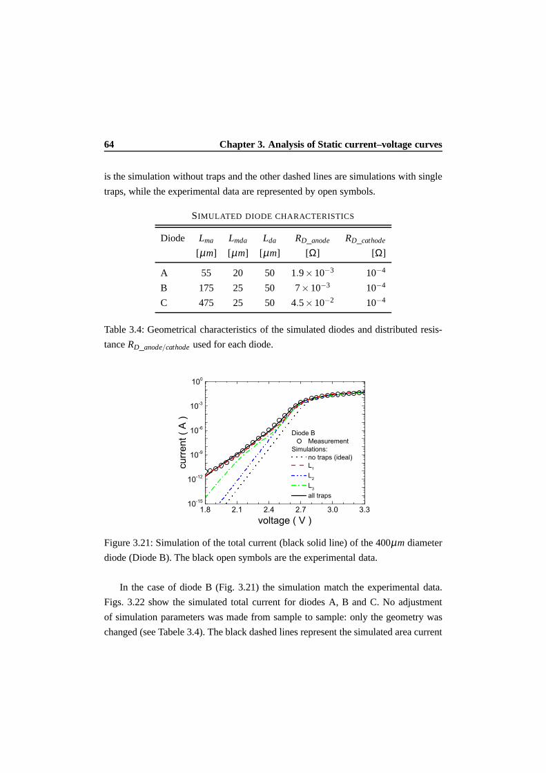
3.21 Simulation of the total current (black solid line) of the 400µm diam-
eter diode (Diode B). The black open symbols are the experimental
data. . . . . . . . . . . . . . . . . . . . . . . . . . . . . . . . . . . 64
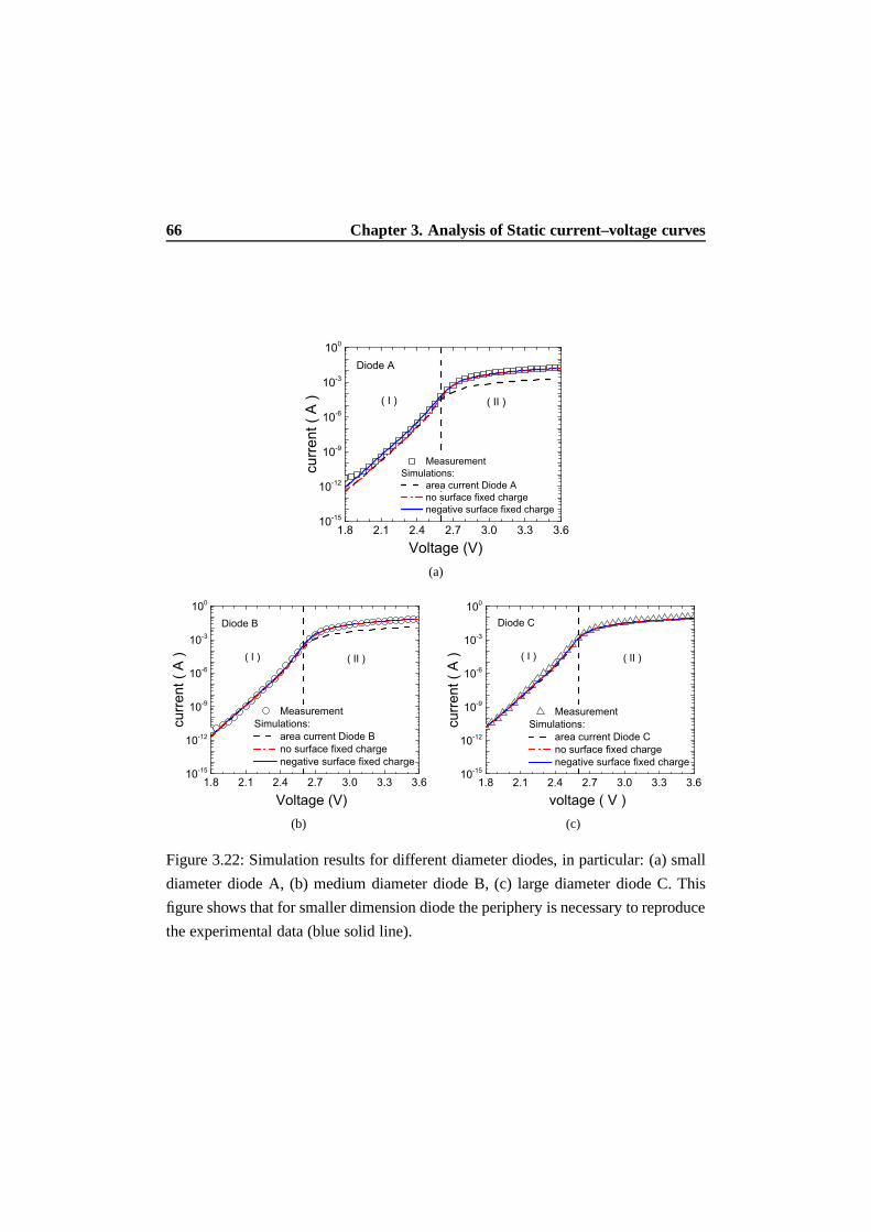
3.22 Simulation results for different diameter diodes, in particular: (a)
small diameter diode A, (b) medium diameter diode B, (c) large di-
ameter diode C. This figure shows that for smaller dimension diode
the periphery is necessary to reproduce the experimental data (blue
solid line). . . . . . . . . . . . . . . . . . . . . . . . . . . . . . . . 66
3.23 SRH recombination rate within the Space Charge Region (SCR), (a)
without any surface fixed charge and (b) with presence of surface
fixed charge. . . . . . . . . . . . . . . . . . . . . . . . . . . . . . . 67
3.24 Simulation of the perimeter current density with (solid red line) and
without (red dashed line) surface fixed charge (see text for details). . 68
4.1 (a) SRH, (b) radiative, (c) Auger recombination mechanisms. . . . . 71
4.2 (a) Ideal schematic circuit for implementing the OCVD measurement
technique, in this case the diode is forward biased with a voltage
source. (b) Different voltage decays after switching off the diode. . . 75
4.3 Schematic block diagram of the experimental set–up usedfor OCVD
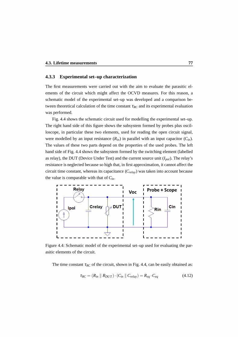
measurements. The central square block represents the PCB.. . . . 76
Page 11
List of Figures vii
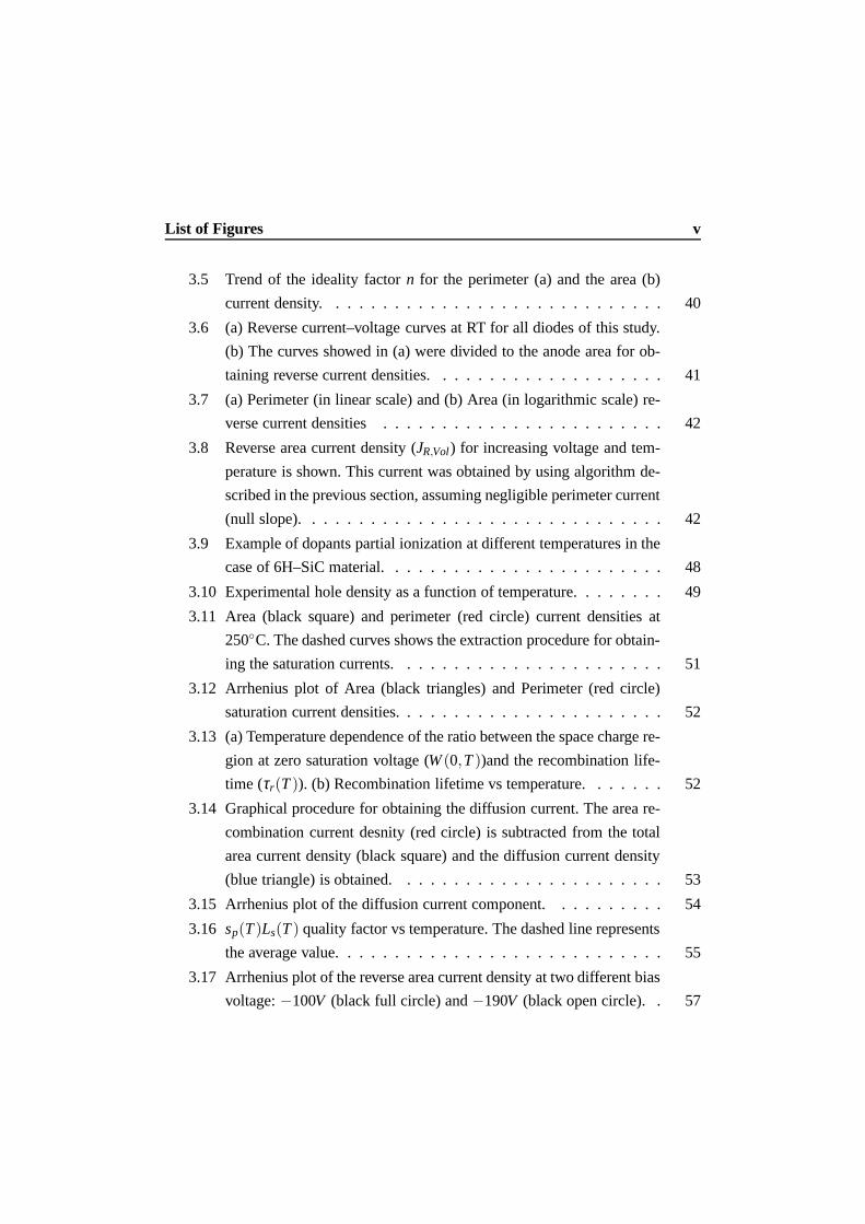
4.4 Schematic model of the experimental set–up used for evaluating the
parasitic elements of the circuit. . . . . . . . . . . . . . . . . . . . 77
4.5 Voltage transient measured (a) with passive probe (b) with active
probe by using differentRDUT . . . . . . . . . . . . . . . . . . . . . 80
4.6 Experimental time constantτRC versusReq = RDUT ‖ Rin, (a) exper-
imental data are fitted for extracting the value ofCeq, (b) the exper-
imental data are fitted by using Eq. (4.12) with expected values of
Ceq. . . . . . . . . . . . . . . . . . . . . . . . . . . . . . . . . . . 81
4.7 Req = RDUT ‖ Rin versusRDUT by usingRin of either passive (black
full squares) or active (red full circles) probes. . . . . . . . .. . . . 82
4.8 Experimental forward current–voltage curves of a 250µm diameter
diode before (red solid line) and after (red dashed line) thewire bond-
ing process. . . . . . . . . . . . . . . . . . . . . . . . . . . . . . . 83
4.9 Schematic model of the experimental set–up consideringa p–n junc-
tion as a DUT. . . . . . . . . . . . . . . . . . . . . . . . . . . . . 84
4.10 Experimental OCVD curves of a 400µm diameter diode measured
by using either passive (red solid line) and active (black solid line)
probes, the blues slid line represents the ideal trend by using a manual
fitting. . . . . . . . . . . . . . . . . . . . . . . . . . . . . . . . . . 85
4.11 Experimental OCVD curves of a 250µm diameter diodes measured
by using active probes for different bias currents. . . . . . . .. . . 86
4.12 (a) Percentage variation of the parallel connection betweenRin and
Rd(V ) with the respect toRd(V ) as a function of the applied voltage
in the case of a 250µm diameter diode. (b) The parallel connection
between the differential diode resistanceRd and the input resistance
Rin (blue dashed line) and the diode differential resistanceRd (red
solid line) are compared, as a function of the applied voltage. . . . . 88
Page 12
viii List of Figures
4.13 As an example, the procedure for extracting the carrierlifetime in the
case of a 250µm diameter diode is shown. The magenta solid line
represents the voltage decay of the diode, the black dashed line the
linear fitting of the voltage decay, the red dashed–dot line represents
the voltage limit. See text for further detail. . . . . . . . . . . .. . 88
4.14 Typical trend of the extractedτA as a function of the applied bias
currentIB for a diode of this study. . . . . . . . . . . . . . . . . . . 89
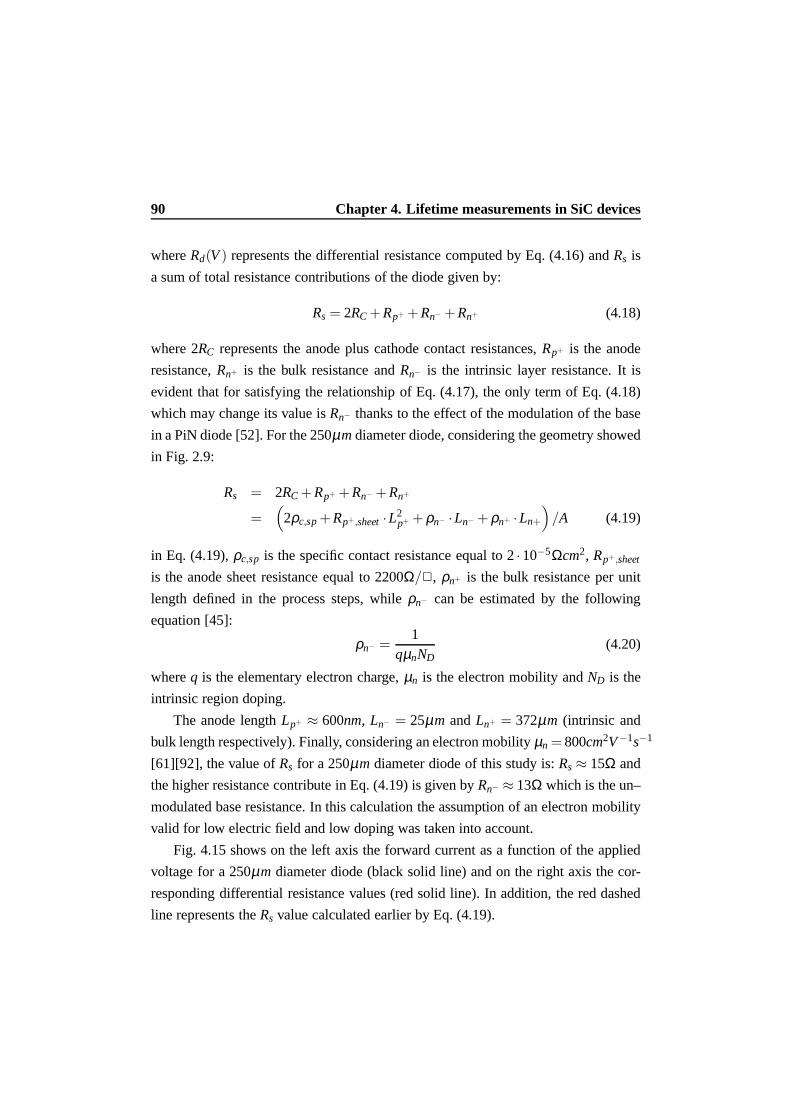
4.15 On the left axis the forward current (black solid line) and on the right
axis the differential resistance (red solid line) of a 250µm diameter
diode are reported. TheRs value plotted (red dashed lines) and the
current level after which the diode enters high injection level (black
dashed–dot line) are also plotted. . . . . . . . . . . . . . . . . . . . 91
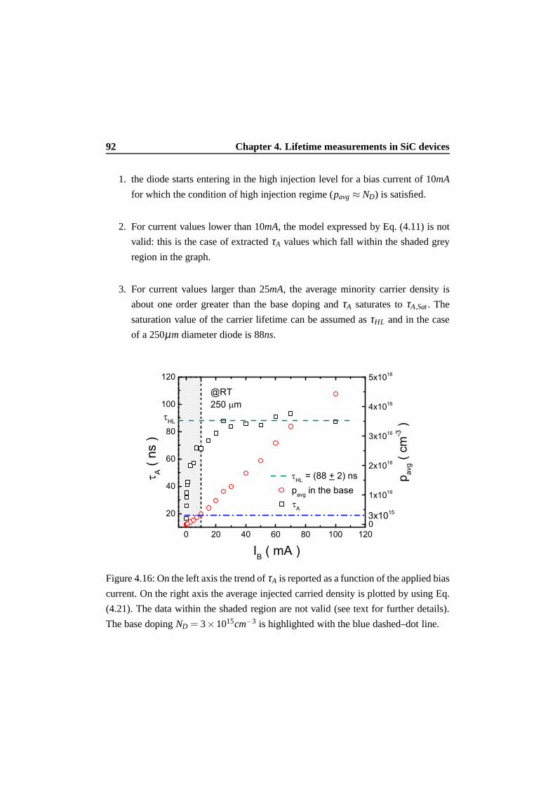
4.16 On the left axis the trend ofτA is reported as a function of the applied
bias current. On the right axis the average injected carrieddensity is
plotted by using Eq. (4.21). The data within the shaded region are
not valid (see text for further details). The base dopingND = 3×
1015cm−3 is highlighted with the blue dashed–dot line. . . . . . . . 92
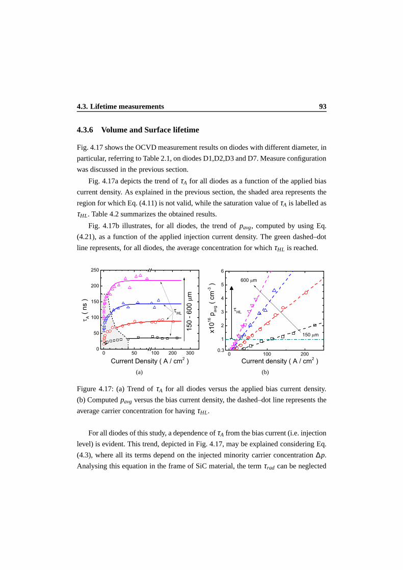
4.17 (a) Trend ofτA for all diodes versus the applied bias current density.
(b) Computedpavg versus the bias current density, the dashed–dot
line represents the average carrier concentration for having τHL. . . 93
4.18 Separation of volume and surface lifetime in the case of(a) surface
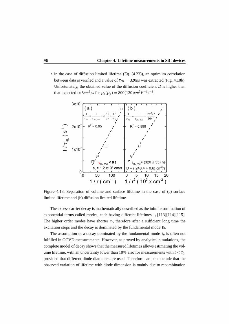
limited lifetime and (b) diffusion limited lifetime. . . . . .. . . . . 96
Page 13
List of Tables
2.1 Labels and dimensions of processed diodes. . . . . . . . . . . .. . 26
3.1 Physical constant and 4H-SiC material properties used in calcula-
tions. . . . . . . . . . . . . . . . . . . . . . . . . . . . . . . . . . 50
3.2 Simulation parameters used for modelling 4H-SiC material. . . . . . 60
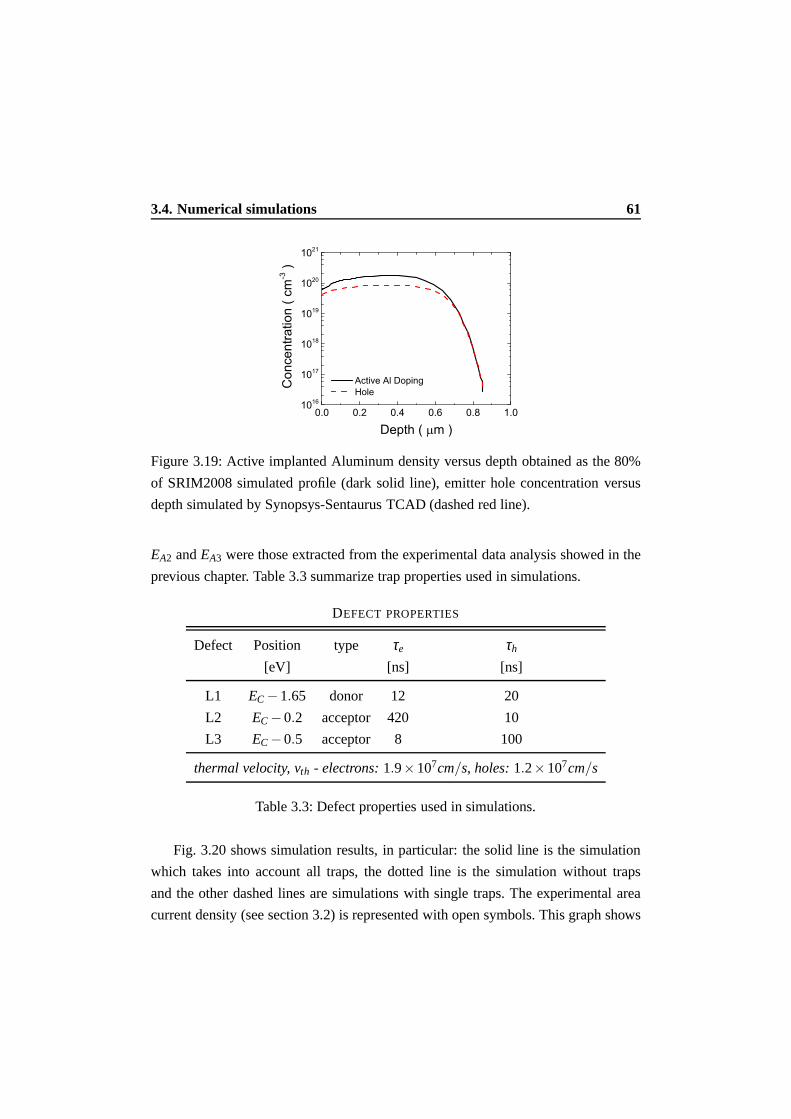
3.3 Defect properties used in simulations. . . . . . . . . . . . . . .. . 61
3.4 Geometrical characteristics of the simulated diodes and distributed
resistanceRD_anode/cathode used for each diode. . . . . . . . . . . . 64
4.1 Time constant values for differentRDUT in the case of passive and
active probes. The bias current is also reported. . . . . . . . . .. . 79
4.2 τHL measurement results. . . . . . . . . . . . . . . . . . . . . . . . 94
Page 15
Introduction
The fast growth of modern societies entails a quick development of electronic tech-
nologies with the aim to improve comfort, transportation and healthcare. These tech-
nological improvements require great advances in power distribution, power genera-
tion and power management technologies.
After the initial replacement of vacuum tubes by solid–state devices in the 1950s,
the related electronic market grew up rapidly. Among all semiconductor, the preferred
for industrial mass production of these devices was Silicon(Si). However, the steadily
increasing request of devices with higher performances andwith smaller dimensions
have led the research efforts in studying new semiconductormaterials suitable for
the production of a new class of devices for high power electronic and high tempera-
ture applications. Thanks to the superior physical properties with respect to Silicon in
terms of critical electric field and thermal conductivity values, Silicon Carbide (SiC)
has attracted the attention of many researchers as a possible candidate for the fabrica-
tion of this new generation of devices with high performanceand small dimensions.
Silicon Carbide is as old as Silicon, it was discovered more than likely by J. J.
Berzelius in the far 1824. After the first synthesis of this compound material, which
occured in the early 1890 by Ancheson, in 1907 its electronicproperties were further
investigated. The basic requirement for a mass industrial production is the growth of
large wafers with electronic grade. Unfortunately, SiC have a complex structure, the
Ancheson was a cumbersome process that required patience and often the purity of
crystals was not controllable. For this reason, the interest in Silicon Carbide as an
electronic material waned up to late 1970s when, thanks to the modified Lely pro-
Page 16
2 Introduction
cess, high quality 6H polytype large wafer were manufactured. After years of further
developments CREE Research was the first company to sell a 2.5cm high quality
6H–SiC wafers and in the 1990s SiC devices entered the electronic market. Since the
mid of 1990s the 4H became the favourite polytype for high power electronic device
production for the higher mobility and higher band–gap withthe respect to the 6H–
SiC. As a result of the rapid progress in SiC wafers growth anddevice fabrication
technologies in the last decade, SiC devices are commonly available in the electronic
market to date.
In this thesis work 4H–SiC ion implanted PiN diodes are studied and charac-
terised in detail. Electrical measurements (current–voltage curves and lifetime mea-
surements) and Numerical simulations are performed with the aim to better under-
stand physical phenomena which arises from the periphery ofthese diodes. This
analysis is relevant as it is well known that perimeter currents affect performances
of SiC devices. This thesis is structured as follows:
• Chapter 1 reports the material properties of the most used SiC polytype for
electronic applications together with a brief historical background of growth
processes of SiC wafers.
• Chapter 2 describes the ion implatation and post–implantation annealing pro-
cesses for selective area doping of SiC material. Furthermore, the issue related
to the ohmic contacts on SiC are also discussed. Finally, theprocessing steps of
the studied devices are listed and their experimental forward and reverse curves
are shown. In this chapter, the experimental set–up used forperforming these
latter measurements is described in detail.
• Chapter 3 describes the analysis methodologies for obtaining the experimental
perimeter and area current density curves. The range of validity of the sim-
ple abrupt–junction model is also analysed before applyingthe method to ex-
perimental area and perimeter curves. From this detailed analysis, important
information are extracted, in particular: defect activation energies responsible
of current transport, the recombination lifetime within the Space Charge Re-
gion and information about the surface quality. Numerical simulations are per-
Page 17
Introduction 3
formed in order to study the origin of periphery currents. Simulations, which
combines detailed experimental data analysis with appropriate literature re-
sults, are proposed and validated.
• Chapter 4 provides a brief explanation of generation and recombination life-
times. The main lifetime measurement techniques used in thecase of Silicon
Carbide devices are reported with particular attention to the Open Circuit Volt-
age Decay (OCVD) which is the method used for this study. A detailed char-
acterization of the experimental measurement set–up is shown and a schematic
circuital model is provided. Comparison between experimental and theoretical
calculations are performed in order to validate the proposed model. Finally,
the experimental OCVD curves of diodes are shown and studiedin detail and
an explanation about the volume and surface lifetimes of these devices is pro-
vided.
Page 19
Chapter 1
Single Crystal Silicon Carbide
1.1 Material Properties
Silicon Carbide (SiC) is a semiconductor which thanks to itsphysical properties is
widely used for fabrication of devices for high temperature, high power and high fre-
quency applications. The outstanding physical propertiesderive from its crystalline
structure, the SiC is a IV–IV compound material with a tetrahedric structure in which
Silicon atoms form almost covalent bondings with the near Carbon atoms (Fig. 1.1,
[1]). The stacking sequence of this elementary cell gives origin to different SiC poly-
types.
Figure 1.1: (a) Elementary structural unit of SiC material.(b) A second type rotated
of 180 around the stacking direction, with respect to (a).
Page 20
6 Chapter 1. Single Crystal Silicon Carbide
The strong chemical bondings together with a particular stacking sequence pro-
vide each polytype with unique electrical and optical properties. Even within a given
polytype, some important electrical properties are non–isotropic, indeed they are a
functions of crystallographic direction of current flow andapplied electric field. Fur-
thermore, SiC is able to form silicon dioxide (SiO2) as a native stable oxide, like
Silicon, and this is an important advantage for device fabrication such as MOSFETs
[2][3][4].
For use as an electronic semiconductor, among all SiC polytypes [5], the ma-
jor efforts of research and development have been concentrated on 3C, 6H, and 4H
polytypes [6]. 3C–SiC, also referred to asβ–SiC, is the only form of SiC with a cu-
bic crystal lattice structure. 4H–SiC and 6H–SiC are only two of many possible SiC
polytypes with hexagonal crystal structure [7].
Fig. 1.2 reports the main physical properties of these threepolytypes compared
to those of the most employed material for electronic devicefabrications, the Silicon.
Figure 1.2: Table reporting the main physical properties ofthe most used SiC poly-
types for electronic application.
Page 21
1.2. SiC Wafers 7
More detailed electrical and optical properties can be found in [8][9].
SiC polytypes exhibit advantages and disadvantages if compared to Silicon. The
most beneficial properties of SiC over Silicon are: higher breakdown electric field,
wider band–gap energy, higher thermal conductivity and higher carrier saturation
velocity (very important for high frequency applications). Compared to the others
two politypes, 4H–SiC is nowadays the preferred for production of electronic devices,
thanks to the superior band–gap and mobility values.
1.2 SiC Wafers
1.2.1 Early history
Most of Silicon Carbide’s superior intrinsic electrical properties with respect to other
semiconductor have been knowing for decades. Nevertheless, for commercial mass–
production of semiconductor electronic devices, large high quality wafers are needed.
SiC sublimes instead of melting and therefore cannot be grown by conventional
techniques such as Czochralski method employed in the manufacturing of almost
all high–quality Silicon large wafers. This prevented the realization of SiC crystals
suitable for electronic device mass–productions until thelate 1980s.
Despite the absence of SiC substrates, the potential benefits of a SiC–based elec-
tronic, for realising devices working in harsh–environment, has led research efforts
to obtain SiC manufacturable wafer.
In the late 1970s, Tairov and Tsvetkov invented a reproducible method for SiC
ingots growth [10][11]. They introduced a 6H–SiC seed into asublimation growth
furnace and designed an appropriate temperature gradient to control mass transport
from the SiC source onto the seed crystal, based on thermodynamic and kinetic con-
siderations. This growth method is called modified Lely or seeded sublimation pro-
cess (and also Physical Vapor Transport, PVT) and it was a breakthrough for SiC as
it offered the first possibility of growing relatively high–quality large–area substrates
of SiC that could be cut and polished into mass-produced SiC wafers.
After years of further development of the sublimation growth process [12], CREE
Research became the first company to sell 2.5cm–diameter semiconductor wafers of
Page 22
8 Chapter 1. Single Crystal Silicon Carbide
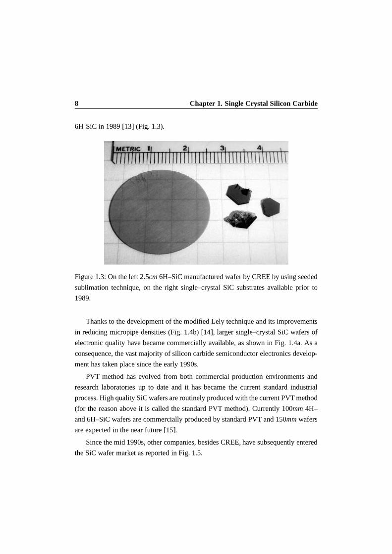
6H-SiC in 1989 [13] (Fig. 1.3).
Figure 1.3: On the left 2.5cm 6H–SiC manufactured wafer by CREE by using seeded
sublimation technique, on the right single–crystal SiC substrates available prior to
1989.
Thanks to the development of the modified Lely technique and its improvements
in reducing micropipe densities (Fig. 1.4b) [14], larger single–crystal SiC wafers of
electronic quality have became commercially available, asshown in Fig. 1.4a. As a
consequence, the vast majority of silicon carbide semiconductor electronics develop-
ment has taken place since the early 1990s.
PVT method has evolved from both commercial production environments and
research laboratories up to date and it has became the current standard industrial
process. High quality SiC wafers are routinely produced with the current PVT method
(for the reason above it is called the standard PVT method). Currently 100mm 4H–
and 6H–SiC wafers are commercially produced by standard PVTand 150mm wafers
are expected in the near future [15].
Since the mid 1990s, other companies, besides CREE, have subsequently entered
the SiC wafer market as reported in Fig. 1.5.
Page 23
1.2. SiC Wafers 9
(a) (b)
Figure 1.4: (a) Increase of wafer size demonstrated by CREE company. (b) Reduction
of micropipes densities in SiC Substrates of different dimension.
Figure 1.5: List of single–crystal SiC wafer providers since early 1990s.
Page 24
10 Chapter 1. Single Crystal Silicon Carbide
1.2.2 SiC Epitaxial Growth
Although sublimation–growth techniques are relatively easy to implement, these pro-
cesses are difficult to control, particularly over large substrate areas [1]. SiC is a ma-
terial having more than 170 polytypes and each polytype shows different properties
(as reported in Fig. 1.2 for the most common polytypes) such as different band–gap
which can range from 2.4eV to 3.3eV [4]. Therefore, a key issue during the growth
of SiC bulk material for electronic applications is the control of polytype. If special
precautions are not taken, during SiC crystals grown by sublimation technique, the
bulk material will contain inclusions of undesirable polytypes. Several technological
parameters impact the final polytype structure of SiC crystals, in particular: super-
saturation of the vapor above growing surface, growth temperature, growth pressure,
seed surface orientation and polarity and presence of impurities. Another important
technological improvement for the realization of SiC electronic devices with complex
structures is the accurate control and type of doping impurities and the thickness of
grown materials [15].
For these reasons, for improving the quality of bulk SiC material and realis-
ing complicated device structures, epitaxial growth methodologies such as liquid–
phase epitaxy (LPE), molecular beam epitaxy (MBE), and chemical vapor deposition
(CVD) have been also investigated.
In 1983 [16][17], the hetero–epitaxial growth of single–crystal SiC layers on top
of large–area silicon substrates was firstly carried out. Unfortunately, hetero–epitaxy
of SiC using Silicon as a substrate always results in growth of 3C-SiC with a very high
density of defects, because of differences in lattice constant and thermal expansion
coefficient between these two materials. For this reason, 3C–SiC has been commonly
used for manufacturing Micro–Electro–Mechanical systems(MEMS)–based sensors
(see as an example [18]), since the performance of electronic devices (Schottky bar-
rier diodes (SBDs), pn diodes, MOSFETs) was far below that expected.
However, strong economic motivation still encourages to improve hetero–epitaxial
growth of SiC on large–area Silicon substrates as this wouldprovide cheap wafers for
productions of SiC electronic devices that would be immediately compatible with sil-
icon integrated circuit.
Page 25
1.2. SiC Wafers 11
In 1987, Matsunami et al. [19] discovered that high–quality6H–SiC can be homo–
epitaxially grown by CVD at relatively low growth temperature, when a several de-
gree off–angle, with respect to the c–axis substrates (obtained by Acheson [20] or
modified Lely processes), is introduced into the 6H–SiC with(0001) orientation, this
technique was called step–controlled epitaxy [21].
Step controlled epitaxy is based upon growing epilayers on aSiC wafer pol-
ished at an angle (called the tilt–angle or off–axis angle) of typically 3 to 8 off the
(0001) basal plane, resulting in a surface with atomic stepsand flat terraces between
steps as schematically depicted in Fig.1.4. When growth conditions are properly con-
trolled and there is a sufficiently short distance between steps, ordered lateral step
flow growth takes place which enables the stacking sequence of the substrate to be
exactly mirrored in the growing epilayer.
Figure 1.6: Schematic view of a step–controlled epitaxial growth.
Homo–epitaxial growth of 6H–SiC on off–axis 6H-SiC (0001) became a standard
technique in the SiC community because it yielded high purity, good in–situ doping
control [22] and uniformity.
In 1993, a high mobility of over 700cm2V 1s1 was first reported for 4H–SiC grown
using this technique [23]. The combination of this result together with the superior
physical properties of 4H-SiC, the commercial release of 4Hpolytype wafers, and
demonstration of excellent devices realised with this material, made 4H–SiC the pre-
ferred choice for electronic device fabrication in the mid 1990s.
In 1995, a hot–wall CVD reactor was proposed by Kordina et al.[24]. This reactor
Page 26
12 Chapter 1. Single Crystal Silicon Carbide
design is currently the standard, because it allows superior control of temperature
distribution, has a much longer susceptor life and better growth efficiency.
1.3 Technological improvements in SiC Growth substrates
SiC devices realised since the 1990s, when the first high quality substrate was man-
ifacured by CREE, began to show performances that in some cases exceeded those
of GaAs or Si devices in high–power and high–temperature applications. As a conse-
quence, physical properties and defects of SiC materials have been extensively inves-
tigated. At the same time, other grown techniques were considered in order to obtain
wafers of higher quality, since substrates are the key elements in the development of
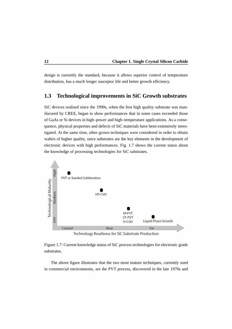
electronic devices with high performances. Fig. 1.7 shows the current status about
the knowledge of processing technologies for SiC substrates.
Figure 1.7: Current knowledge status of SiC process technologies for electronic grade
substrates.
The above figure illustrates that the two most mature techniques, currently used
in commercial environments, are the PVT process, discovered in the late 1970s and
Page 27
1.3. Technological improvements in SiC Growth substrates 13
the HT–CVD proposed more recently, as discussed in the previous section.
Other promising techniques are the Continuous Feed PVT (CF–PVT) [25], Halide
CVD (H–CVD) [26], and Modified PVT (M–PVT) [27]. Although these latter growth
techniques might have some technological edges over their predecessors, they are still
at the research stage.
Solution phase growth has yet to prove its capability of producing large area
substrates. Nonetheless, promising initial results and the advantages of this method
will certainly draw more attention from the research and industrial community.
Page 29
Chapter 2
Ion Implanted vertical 4H-SiC PiN
diodes
2.1 Ion Implantation
Diffusion and Ion implantation are fundamental processes for introducing impurities
in a semiconductor wafer through windows that are opened in selected regions of a
mask film that is deposied, or grown, on the surface of the semiconductor wafer itself.
In the case of Silicon Carbide, because of its very strong chemical bonding, diffu-
sion constants of impurities are extremely small. For this reason, a significant diffused
dopant–depth profile requires both very high temperatures (larger than 2000C) and
relatively long times. Under these conditions, it is hard tofind a good material for the
fabrication of a sufficiently resistant diffusion mask, moreover, the decomposition
of SiC at such high temperatures, as well as the formation of intrinsic and extended
defects, are strongly favoured. The development of ion implantation processing for
the selected area doping of SiC wafers is of major importancefor obtaining: source
or drain regions, junction termination, channel doping, p-body of FET devices,p+
contact and p-n junction [2][28][29].
The most common dopants for SiC are Aluminum (Al) and Boron (B) for ob-
taining p-type doped regions, whereas Nitrogen (N) and Phosphorus (P) are used
Page 30
16 Chapter 2. Ion Implanted vertical 4H-SiC PiN diodes
for n-type doped regions. Implant profiles can be scheduled either by Monte Carlo
simulations of the ion implantation process in software such as SRIM (Stopping and
Range of Ions in Matter) [30], or, much better, by Pearson IV algorithms [31] which
take into accounts experimental database for the differentmomenta of the ion depth
distribution such as those in [32]. In both the cases, simulation outputs concern ion
implantation processes along a random direction. The implantation geometry into
a crystal is defined as random when the incidence ions experience as many energy
losses and collisions as they would have in the same materialbut with amorphous
structure [3].
The convention for identifying implantation geometries islinked to tilt and twist
angles with respect to the wafer normal and the wafer flat, respectively. The tilt angle
can be defined as the rotation angle in the direction of the wafer normal with respect
to the ion beam incidence, whereas the twist angle is the rotation angle of the wafer
around its normal, as shown in Fig. 2.1. The tilt and twist angle values depend on the
relative position of the semiconductor lattice structure with respect to the wafer plane
and on the ion species, ion energy, and ion beam direction.
Figure 2.1: Illustration of tilt and twist angles for defining implantation geometry.
See text for further details.
Page 31
2.1. Ion Implantation 17
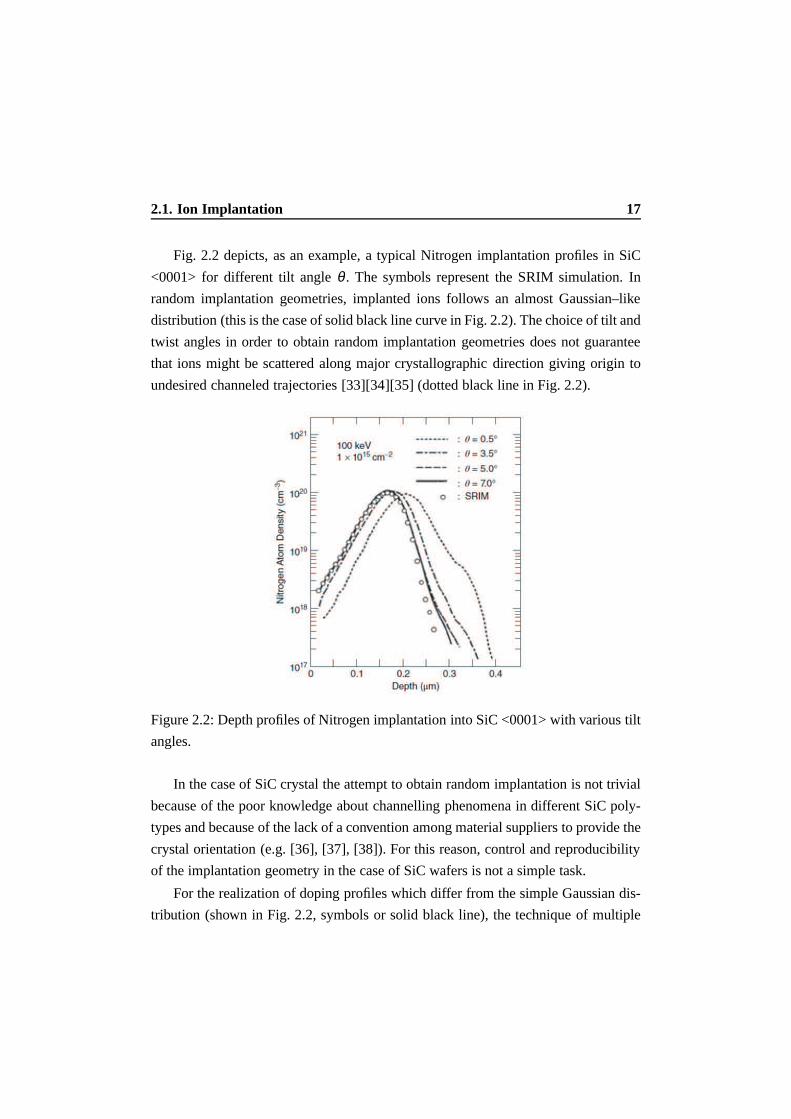
Fig. 2.2 depicts, as an example, a typical Nitrogen implantation profiles in SiC
<0001> for different tilt angleθ . The symbols represent the SRIM simulation. In
random implantation geometries, implanted ions follows analmost Gaussian–like
distribution (this is the case of solid black line curve in Fig. 2.2). The choice of tilt and
twist angles in order to obtain random implantation geometries does not guarantee
that ions might be scattered along major crystallographic direction giving origin to
undesired channeled trajectories [33][34][35] (dotted black line in Fig. 2.2).
Figure 2.2: Depth profiles of Nitrogen implantation into SiC<0001> with various tilt
angles.
In the case of SiC crystal the attempt to obtain random implantation is not trivial
because of the poor knowledge about channelling phenomena in different SiC poly-
types and because of the lack of a convention among material suppliers to provide the
crystal orientation (e.g. [36], [37], [38]). For this reason, control and reproducibility
of the implantation geometry in the case of SiC wafers is not asimple task.
For the realization of doping profiles which differ from the simple Gaussian dis-
tribution (shown in Fig. 2.2, symbols or solid black line), the technique of multiple
Page 32
18 Chapter 2. Ion Implanted vertical 4H-SiC PiN diodes
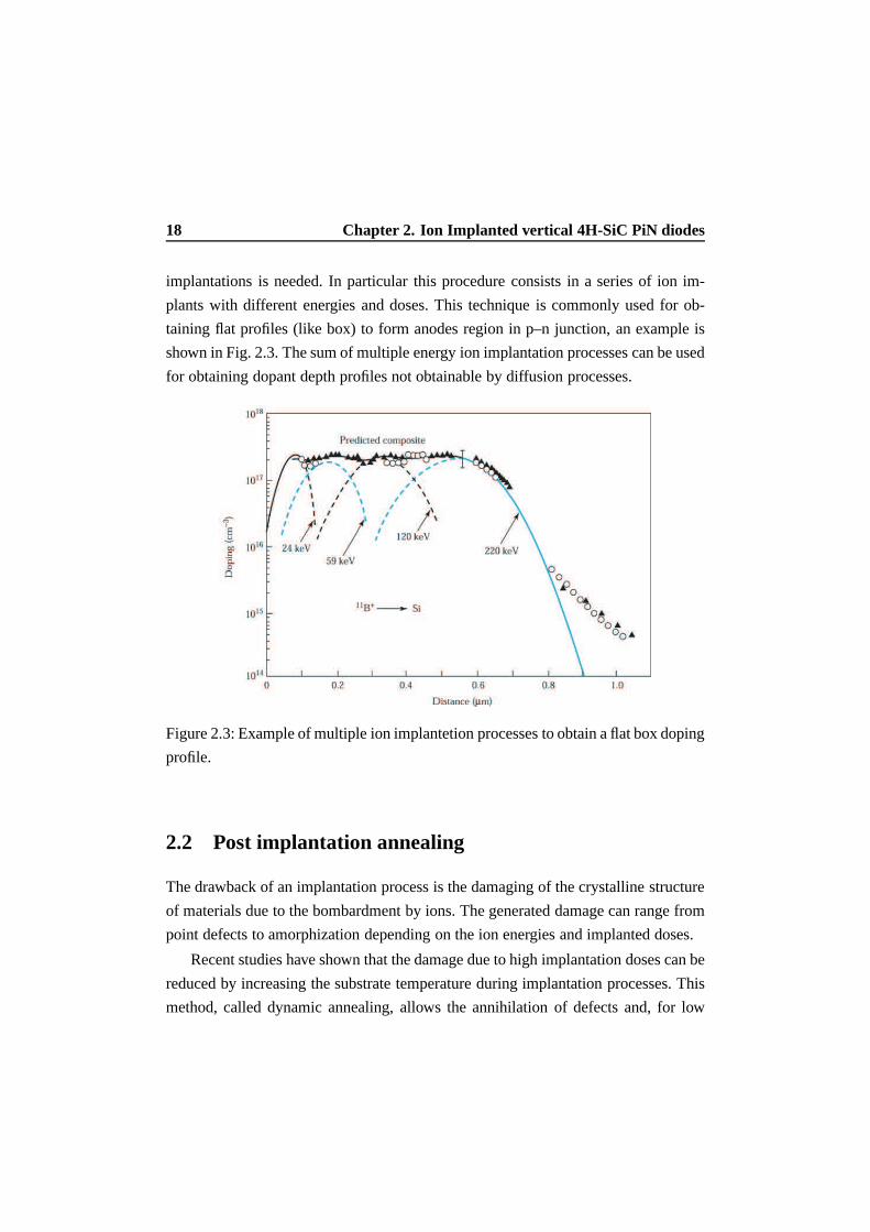
implantations is needed. In particular this procedure consists in a series of ion im-
plants with different energies and doses. This technique iscommonly used for ob-
taining flat profiles (like box) to form anodes region in p–n junction, an example is
shown in Fig. 2.3. The sum of multiple energy ion implantation processes can be used
for obtaining dopant depth profiles not obtainable by diffusion processes.
Figure 2.3: Example of multiple ion implantetion processesto obtain a flat box doping
profile.
2.2 Post implantation annealing
The drawback of an implantation process is the damaging of the crystalline structure
of materials due to the bombardment by ions. The generated damage can range from
point defects to amorphization depending on the ion energies and implanted doses.
Recent studies have shown that the damage due to high implantation doses can be
reduced by increasing the substrate temperature during implantation processes. This
method, called dynamic annealing, allows the annihilationof defects and, for low
Page 33
2.2. Post implantation annealing 19
ion fluxes, defect densities can never reach the critical value for having the material
amorphization. The schematic representation in Fig. 2.4 shows the effect of dynamic
annealing: in particular by increasing the substrate temperature, higher implanted
doses can be tolerated before material reaches the amorphization.
Figure 2.4: Schematic example of dynamic annealing. Increasing the substrate tem-
perature a higher ion flux is tolerated during ion implantation processes.
However, for recovering the damaged lattice and for electrically activating the
implanted dopants, post implantation annealing processes, at an appropriate combi-
nation of time and temperature, are mandatory after the ion implantation [39]. In
the case of SiC, the understanding and accurate control of such a process is still a
scientific challenge [3].
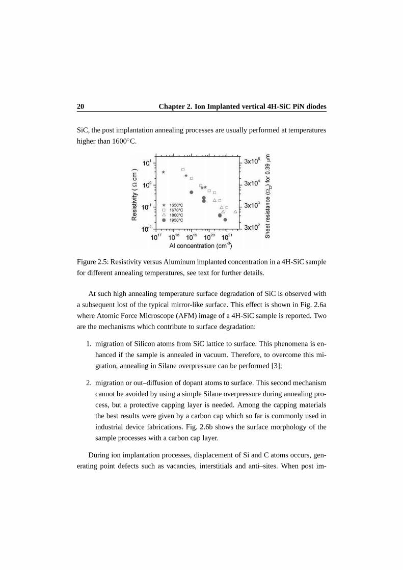
As an example, Fig. 2.5 depicts the resistivity as a functionof Al concentration
in a 4H–SiC sample [40] for different post implantation annealing temperatures. This
figure illustrates that the higher the annealing temperature the lower the resistivity of
the material. In particular, the resistivity of a material is the inverse of conductivity
which, in turn, is directly proportional to the free carrierconcentration. Therefore, the
lower the resistivity the higher the free carrier concentration and, besides the dopant
partial ionization, the higher the electrical activation.For this reason, in the case of
Page 34
20 Chapter 2. Ion Implanted vertical 4H-SiC PiN diodes
SiC, the post implantation annealing processes are usuallyperformed at temperatures
higher than 1600C.
Figure 2.5: Resistivity versus Aluminum implanted concentration in a 4H-SiC sample
for different annealing temperatures, see text for furtherdetails.
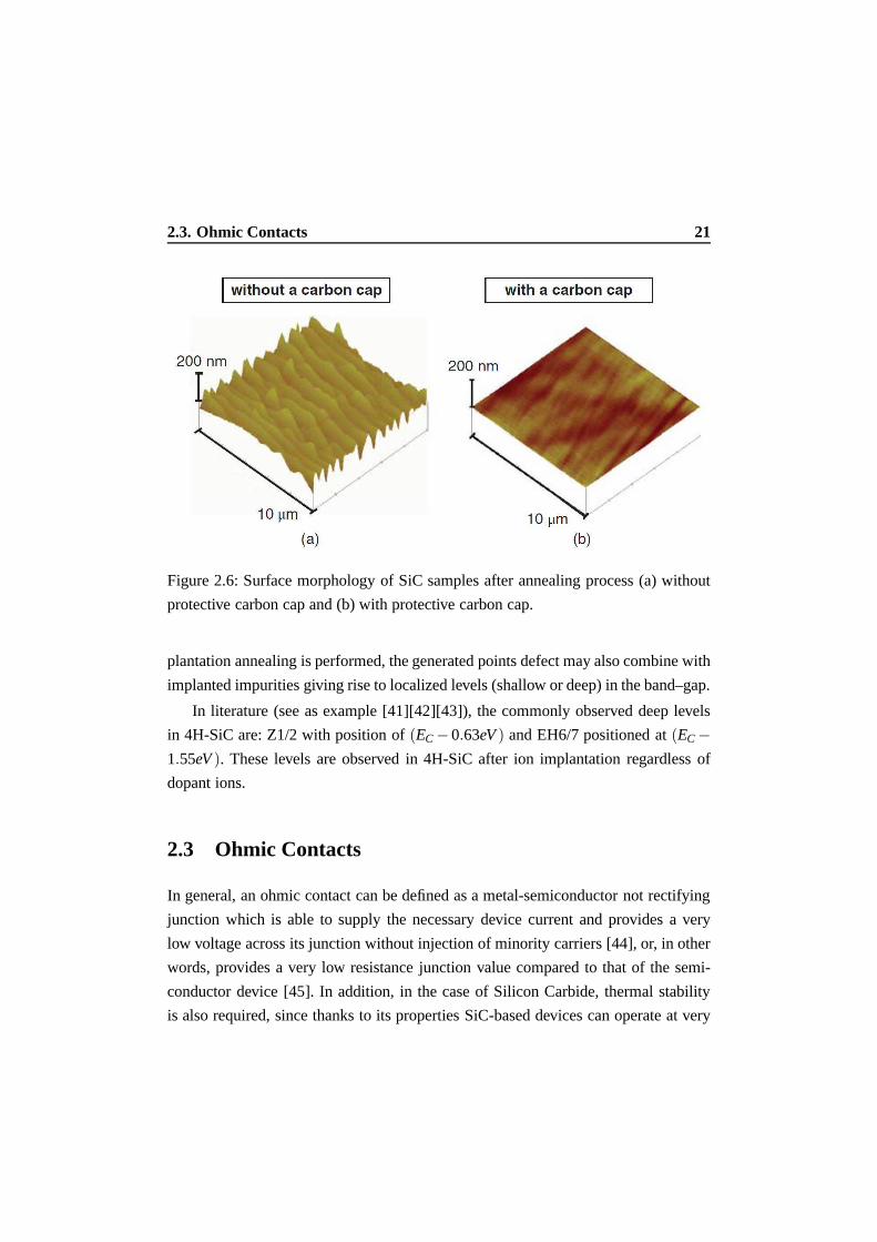
At such high annealing temperature surface degradation of SiC is observed with
a subsequent lost of the typical mirror-like surface. This effect is shown in Fig. 2.6a
where Atomic Force Microscope (AFM) image of a 4H-SiC sampleis reported. Two
are the mechanisms which contribute to surface degradation:
1. migration of Silicon atoms from SiC lattice to surface. This phenomena is en-
hanced if the sample is annealed in vacuum. Therefore, to overcome this mi-
gration, annealing in Silane overpressure can be performed[3];
2. migration or out–diffusion of dopant atoms to surface. This second mechanism
cannot be avoided by using a simple Silane overpressure during annealing pro-
cess, but a protective capping layer is needed. Among the capping materials
the best results were given by a carbon cap which so far is commonly used in
industrial device fabrications. Fig. 2.6b shows the surface morphology of the
sample processes with a carbon cap layer.
During ion implantation processes, displacement of Si and Catoms occurs, gen-
erating point defects such as vacancies, interstitials andanti–sites. When post im-
Page 35
2.3. Ohmic Contacts 21
Figure 2.6: Surface morphology of SiC samples after annealing process (a) without
protective carbon cap and (b) with protective carbon cap.
plantation annealing is performed, the generated points defect may also combine with
implanted impurities giving rise to localized levels (shallow or deep) in the band–gap.
In literature (see as example [41][42][43]), the commonly observed deep levels
in 4H-SiC are: Z1/2 with position of(EC −0.63eV ) and EH6/7 positioned at(EC −
1.55eV ). These levels are observed in 4H-SiC after ion implantationregardless of
dopant ions.
2.3 Ohmic Contacts
In general, an ohmic contact can be defined as a metal-semiconductor not rectifying
junction which is able to supply the necessary device current and provides a very
low voltage across its junction without injection of minority carriers [44], or, in other
words, provides a very low resistance junction value compared to that of the semi-
conductor device [45]. In addition, in the case of Silicon Carbide, thermal stability
is also required, since thanks to its properties SiC-based devices can operate at very
Page 36
22 Chapter 2. Ion Implanted vertical 4H-SiC PiN diodes
high-temperature.
Fig. 2.7 shows the 4H-SiC band diagram referring to the vacuum level. Ideally,
for having an ohmic contact, a metal with work functionqΦm lower thanqχs for n–
type material or higher thanqχs +Eg for p–type material is required. In these cases,
the carriers can flow in both directions without encountering any Schottky barrier.
Figure 2.7: Band diagram of 4H-SiC.
However, almost all metals have a work functionΦm between 5÷6eV and there-
fore, as shown in Fig. 2.7, in 4H-SiC ideal ohmic contacts cannot be realized espe-
cially on p–type material [46]. To overcome this problem in the case of wide band–
gap materials, the common strategies to form low resistivity ohmic contacts is by
using the tunnelling current phenomena [2].
In general, the as-deposited Metal–SiC contacts are non ohmic but with rectifying
properties because of the high value of the Schottky barrier. Therefore, besides to the
creation of highly doped layers for tunnelling phenomena and the accurate choice of
a metal which may form a low barrier height, a post depositionannealing process at
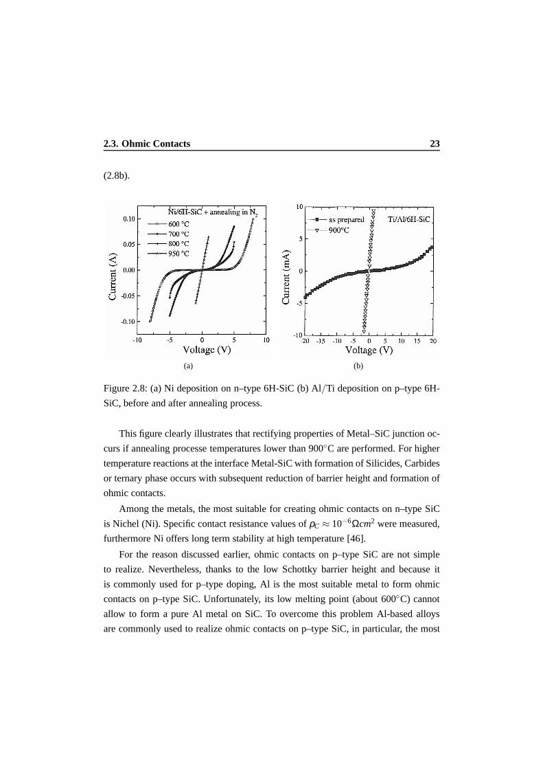
temperature in the range 900÷ 1000C is required. As an example, Fig. 2.8 shows
electrical Trasmission Line Model (TLM) measurements of as-deposited and after
annealing process of Ni on n–type 6H-SiC (2.8a) and of Al/Ti on p–type 6H-SiC
Page 37
2.3. Ohmic Contacts 23
(2.8b).
(a) (b)
Figure 2.8: (a) Ni deposition on n–type 6H-SiC (b) Al/Ti deposition on p–type 6H-
SiC, before and after annealing process.
This figure clearly illustrates that rectifying propertiesof Metal–SiC junction oc-
curs if annealing processe temperatures lower than 900C are performed. For higher
temperature reactions at the interface Metal-SiC with formation of Silicides, Carbides
or ternary phase occurs with subsequent reduction of barrier height and formation of
ohmic contacts.
Among the metals, the most suitable for creating ohmic contacts on n–type SiC
is Nichel (Ni). Specific contact resistance values ofρC ≈ 10−6Ωcm2 were measured,
furthermore Ni offers long term stability at high temperature [46].
For the reason discussed earlier, ohmic contacts on p–type SiC are not simple
to realize. Nevertheless, thanks to the low Schottky barrier height and because it
is commonly used for p–type doping, Al is the most suitable metal to form ohmic
contacts on p–type SiC. Unfortunately, its low melting point (about 600C) cannot
allow to form a pure Al metal on SiC. To overcome this problem Al-based alloys
are commonly used to realize ohmic contacts on p–type SiC, inparticular, the most
Page 38
24 Chapter 2. Ion Implanted vertical 4H-SiC PiN diodes
employed are Al/Ti alloys and its modification (e.g. Al/Ti/Ni) [2].
The sintering process for obtaining good ohmic contacts on p–type SiC is still a
scientific challenge, in particular the conservation of form factor and thickness of the
chemically reacted layer at the interface Metal-SiC are still open issues (e.g. [47]).
2.4 Process steps
A <0001> 8 off–axis 4H–SiC n–type homo–epitaxial commercial wafers [13] was
used to fabricate vertical p+–i–n− diodes.
The n− epi–layer thickness and doping are 25µm and 3×1015cm−3, respectively.
The n–type bulk wafer is 372µm thick and has a resistivity of 0.021Ωcm.
The p+ anodes are circular with different diameters in the range 150÷1000µm
and have been obtained by multiple-energies Al+ ion implantation processes at 400C
on selected areas. The implantation schedule has been fixed on the base of SRIM2008
simulation outputs [30] for obtaining an almost flat 2.5× 1020cm−3 Al depth box
profile thick about 0.57µm.
Post–implantation annealing process has been performed inside an inductively–
heated graphite crucible in a high–purity Ar atmosphere at 1950C for 5 min. The
heating rate was 40C/s and the cooling rate was exponential with a characteristic
time of about 3 min.
A resist film pyrolyzed in a forming gas ambient (C-cap) [48] has protected the
wafer surface during post–implantation annealing and was later removed by 850C/15
min dry oxidation.
Ohmic contacts on the p+–implanted anodes and on the n+ bulk cathode have
been formed with Ti/Al (80 nm/350 nm) and Ni (150 nm), respectively. Contacts
were alloyed at 1000C/2min in vacuum. After alloying, the anode contacts were
covered by a sputtered 350 nm Al(2%Si) film. The contacts on p+ are circular, con-
centric with the anodes and 40-50µm smaller in diameter than the anode. The Ni
cathode contact extends all over the wafer back surface.
Previous studies on the electrical activation [49] and the surface roughness [50] of
Al+ implanted 4H-SiC specimens have shown a root mean square surface roughness
Page 39
2.5. Static electrical measurements 25
≤ 2nm and an Al electrical activation of about 80% with a compensation of about
20% for 4H-SiC samples doped as the diode’s emitters of this study.
2.5 Static electrical measurements
2.5.1 Device schematic cross–sections and selection criteria
The studied diodes were placed, together with other test structures such as TLM for
specific contact resistance measurements and VdP (Van der Pauw) for electrical acti-
vation measurements, on chips with dimension of 5×7mm. The image representing
the elementary cell which repeats over all the wafer is shownin the bottom of Fig.
2.9. Table 2.1 summarize anode (diameter) and metal dimensions of on–chip diodes.
In this Table, the column labelled(D−M)/2 (whereD is the Diameter, andM the
Metal) reports the distance between metal edge and the end ofdiode anodes. For all
diodes, besides D7, this distance is 25µm, while for the 150µm diameter diode D7 is
20µm.
Devices have been fabricated in the clean–room facility of National Research
Council, Institute of Micro–electronics and Micro–systems, Bologna Unit (CNR–
IMM UOS Bologna) [51], by using processes described in the previous section. A
schematic cross–section of processed diodes is shown in thetop of Fig. 2.9.
2.5.2 Experimental Setup description
Static forward and reverse current-voltage characteristics were measured by using
a home assembled wafer–level parametric characterizationsystem. Measurements
were performed in air at different temperatures. The minimum temperature was 30C
whereas the maximum 290C, the other measurement temperatures range between
50÷250C with a step of 50C. All the measurement instruments were remote con-
trolled by GPIB 488 protocol and a Keithley 707a switching matrix and configured
by using the commercial software ICS (Integrated Controll System).
Forward current measurements were performed by using two Keithley SMUs
(Source/Measure Units) model 238 in particular: the first connected to the thermo–
Page 40
26 Chapter 2. Ion Implanted vertical 4H-SiC PiN diodes
DIMENSION OF PROCESSED DIODES
Label Diameter Metal (D−M)/2 number
– [µm] [µm] [µm] –
D7 150 110 20 4
D1 250 200 25 4
D2, D6 400 350 25 8
D3 600 550 25 4
D4 800 750 25 3
D5 1000 950 25 3
Table 2.1: Labels and dimensions of processed diodes.
Figure 2.9: In the top a schematic cross section of the studied diodes and in the bottom
a processed chip containing the studied devices are shown.
Page 41
2.5. Static electrical measurements 27
chuck for fixing the reference voltage at 0V , the second to the probe tip placed on
device anodes. The maximum applied voltage was 3.9V and the minimum step for
performing the voltage sweep was 30mV . This latter values ensured a stable output
of the SMU. A study on delay time between the voltage application and the current
reading was performed and an optimum delay of 4s was found. This time is sufficient
to avoid apparent leakage currents due to transients of parasitic connection elements.
By using the described measurement configuration a current floor of 5×10⁻¹⁴A was
measured at Room Temperature (RT).
Since very low reverse currents are expected in the case of SiC devices, the Keith-
ley Sub–femto–amperometer model 6430 was used for reverse measurements on the
studied diodes. In this case for minimizing the influence of parasitic leakage cur-
rents, the instrument was directly connected to the thermo–chuck avoiding switching
matrix connections. The maximum reverse bias voltage was−190V and sweep step
was−10V . A study on the delay time, similar to that of forward currentmeasure-
ments, was performed and a delay time of 300s was applied for this measurements
with a current reading each 5s in order to observe the trend of experimental data as a
function of time. In this case a current floor of≈ 5×10⁻¹⁵A was measured at RT.
2.5.3 Diode selection criteria
Among all devices on wafer, only few diodes with precise properties were measured
at different temperatures. In particular, the following criteria was adopted for select-
ing the good devices:
• forward characteristic study: only diodes with no shunt current at low voltages
and with higher current in ohmic region at the minimum measurement temper-
ature (i.e. 30C) were selected;
• reverse characteristic study: only diodes with the lower reverse current at the
maximum bias voltage (190V ) and with no evidence of break–down trend at
the maximum measurement temperature (i.e. 290C) were selected.
By adopting the above selection criteria, after a first screening, one diode for each
Page 42
28 Chapter 2. Ion Implanted vertical 4H-SiC PiN diodes
dimension among those listed in 2.1, were considered. In particular, diodes D7, D2,
D3 and D5 were characterized at all temperatures for forwardstudy, whereas diodes
D7, D2 ad D3 for reverse study.
2.5.4 Experimental measurements
Fig. 2.10 shows a typical current–voltage curves of diodes selected by using the cri-
teria described earlier, in particular: Fig. 2.10a shows the forward current–voltage
curves in the case of linear scale, whereas Fig. 2.10b in logarithmic scale, for 400µm
diameter diode for some measurement temperatures. In thesefigure the instrumental
current floor of 5×10⁻¹⁴A at RT is represented by the grey dashed region.
In the case of linear scale, it is worthwhile pointing out that the diode enters
the high–injection regime. In particular, after switchingon, a typical exponential–
like trend of the current–voltage curve for each temperature can be observed. This
trend indicates that the resistance of the diode base is lowering because of typical
modulation of the PiN diode base [52][53].
0 2 4
0
20
40
60
80
100
400 m
30°C 100 200 290
forw
ard
curre
nt (
mA
)
forward voltage (V)
(a)
0 2 410-14
10-12
10-10
10-8
10-6
10-4
10-2
100
30°C 100 200 290
forw
ard
curre
nt (
A )
forward voltage (V)
400 m
(b)
Figure 2.10: (a) Linear scale and (b) log scale current–voltage characteristic of a
400µm diameter diode of this study, for varying temperatures.
In the case of logarithmic scale, the curves have no evidenceof shunt currents
at low voltages and, after switching on, clearly show two different exponential trend
Page 43
2.5. Static electrical measurements 29
before entering the ohmic region. Under the assumption thatthe forward current can
be modelled by using the following equation:
I(V,T ) = I0 ·
[
exp
(
qVnkT
)
−1
]
(2.1)
whereI0 is the saturation current (or zero voltage current),q is the electron charge,
V the applied voltage,k the Boltzmann constant,T the absolute temperature andn
the ideality factor. The estimation ofn as a function of voltage and temperature is
straightforward, in particular, considering Eq. (2.1),n can be expressed as:
n(V,T ) =1
kTq
d[ln I(V,T )]dV
(2.2)
By using Eq. 2.2, the trend of the ideality factor, of forwardcurrent–voltage curves
showed in Fig. 2.9, is obtained as a function of the applied voltage and for each mea-
surement temperature. This plot illustrates that the current curves show a trait with
ideality factorn equal 2 for almost all temperatures at low voltages, never passing
through 1 before entering the ohmic region. This trend has been observed for all the
studied diodes.
As an example, Fig. 2.12 illustrates the data analysis method for the reverse cur-
rent in the case of 400µm diameter diode for two fixed voltages: 20V Fig. 2.12a and
180V Fig. 2.12b at the fixed temperature of 150C (the same analysis was performed
for all diodes at all temperatures and for all bias voltages).
In particular, static current values have been obtained by studying the current
as a function of time. It has been observed that the thermo–dynamic equilibrium of
devices in the case of low bias voltage (for all temperatures) is reached after 300s
(Fig. 2.12a), whereas for higher bias voltages and high temperature the the thermo–
dynamic equilibrium is reached almost immediately (Fig. 2.12b). This means that for
low voltages and low temperatures the current measurementsare mainly influenced
by the parasitic transients due to connections. The influence of transients become less
important when the measured current signal increases (Fig.2.12b), therefore devices
reach the equilibrium faster with the increasing currents.
Page 44
30 Chapter 2. Ion Implanted vertical 4H-SiC PiN diodes
0.6 1.2 1.8 2.4 3.01.0
1.2
1.4
1.6
1.8
2.0
2.2
forward voltage (V)
30°C 100 200 290
Idea
lity
Fact
or
400 m
Figure 2.11: Trend of ideality factor of curves showed in Fig. 2.10.
0 100 200 300-0.5
-0.4
-0.3
-0.2
-0.1
0.0
0.1
I REV
( 20
V,15
0°C
) (
pA
)
time ( s )
400 m
(a)
0 100 200 300-13.0
-12.9
-12.8
-12.7
-12.6
-12.5
I REV
(-18
0V, 1
50°C
) (p
A)
time ( s )
400 m
(b)
Figure 2.12: Example of data analysis for two different reverse bias voltage (a) 20V
and (b) 180V for the fixed temperature of 150C for a 400µm diameter diode.
Page 45
2.5. Static electrical measurements 31
For a more accurate estimation of the reverse current, especially at low voltages,
the value of the current measured at 0V bias voltage, which takes into account for
the noise current due to the instrumental offset voltage, has been subtracted from all
currents obtained at other bias voltages at all temperatures, in particular:
Irev(V,T ) = Irev_meas(V,T )− Irev_meas(0,T ) (2.3)
where in Eq. (2.3)Irev_meas(V,T ) is the measured reverse current at the bias voltage
V and at the temperatureT .
Fig. 2.13 depicts a typical reverse current characteristicof a 400µm diameter
diode at different temperatures. The characteristics of all diodes have similar trend
and have been obtained by using the method described above. The grey dashed box
points out the region above which the measured current has a reliable values (i.e.
above the instrumental current floor). Data within the box orat its boundary have
been obtained as a consequence of the operation by using Eq. (2.3), for this reason
these experimental data were excluded for data analysis.
0 50 100 150 20010-15
10-14
10-13
10-12
10-11
10-10
10-9 290°C
reverse voltage ( V )
I rev(T
) ( A
)
400 m30°C
Figure 2.13: Typical reverse characteristic of a diode of this study for all the mea-
surement temperatures.
Page 47
Chapter 3
Analysis of Static current–voltage
curves
3.1 Motivations
The common way for obtaining the area current density from forward or reverse
current–voltage characteristics of devices is to divide the measured current by the
active area of device itself:
J(V,T ) = Imeas(V,T )/A (3.1)
Nevertheless, the above relationship has validity only if the measured current
originates from the device volume, in other words only if periphery effects are in-
significant.
It is well–known that, in the case of Silicon Carbide devices, the periphery con-
tribution to the total measured current is not negligible and indeed its importance has
been claimed several times (see as an example [54][55][56]). However, few are the
studies which shows the separation and the accurate analysis of periphery and volume
current components in forward and reverse bias in the case ofSiC devices.
The aim of this thesis work is to provide a methodology for deeply studying the
current–voltage characteristics of SiC devices in order toobtain a better comprehen-
Page 48
34 Chapter 3. Analysis of Static current–voltage curves
sion of such a device performances and reliable estimates ofthe physical parameters
which can help to improve the device fabrication processing.
In the following sections area and volume currents have the same meaning, as the
device volume is the volume which lies below the device active area, in particular: for
the diodes of this study is the volume which lies under the diode anodes. Therefore,
the area or volume current is the current which flows through the area which defines
the volume or which flows in the volume with a section equal to the active area.
3.2 Extraction of Area and Periphery current densities
3.2.1 Theoretical background I
The measured current of a planar diode,Imeas(V,T ), which is voltage(V ) and tem-
perature(T ) dependent, can be written as a sum of several contributions,in particular
[57]:
Imeas(V,T ) = AJarea(V,T )+PJper(V,T )+CIcor(V,T )+ Ipar(V,T ) (3.2)
where:
• A andP are Area and Perimeter of the planar junction interface, i.e. Area and
Perimeter of the anode, respectively;
• C is the number of corners atP;
• Jarea(V,T ) andJper(V,T ) are the current densities per unit areaA and per unit
length of the perimeterP, respectively. More precisely:Jarea(V,T ) is the cur-
rent which flows in the volume defined by the junction area of devices and
Jper(V,T ) is the current which flows in the periphery of devices;
• Icor(V,T ) is the current value per corner;
• Ipar(V,T ) is a contribution that takes into account parasitic currents of the mea-
surement system.
Page 49
3.2. Extraction of Area and Periphery current densities 35
Icor(V,T ) depends on the device geometry andIpar(V,T ) depends on the used instru-
mental set–up.
In this study, vertical planar 4H-SiC p-i-n diodes with circular emitters of differ-
ent diameters (see Chapter 2, Table 2.1) were characterized. This geometry allows
to neglect theCIcor(V,T ) term in Eq. (3.2). Moreover, forward and reverse current-
voltage measurements were performed with two instrumentalset–up with current
floors of 5×10⁻¹⁴A and 5×10⁻¹⁵A, respectively, in the whole voltage and temper-
ature ranges of measurements (see Chapter 2, section 2.5.2). Therefore, in the case
of forward bias,Ipar(V,T ) term in Eq. (3.2) was neglected as its value is very small
compared to that of the measured current (see Fig. 2.10b).
In conclusion, considering thatA = πr2 andP = 2πr, wherer is the anode radius,
Eq. (3.2) can be written as:
Imeas(V,T )≈ πr2Jarea(V,T )+2πrJper(V,T ) (3.3)
When all terms of Eq. (3.3) are divided by the junction areaA = πr2, the following
equation is obtained:
Imeas(V,T )
πr2 = Jarea(V,T )+ Jper(V,T )2r
(3.4)
Making a plot of the measured current divided by the emitter Area (πr2) versus the
Perimeter–Area ratio (2/r) for each voltage and at a fixed temperature, the separation
of Area and Perimeter current densities is obtained. In particular, by using a linear
fitting on the so obtained curves, the intercept of the straight line gives the Area
current density and its slope the Perimeter current density. From Eq. (3.4) it is evident
that:
∀V > 3k/T,Imeas(V,T )
πr2 ≡ Jarea(V,T ) ⇐⇒ Jper(V,T )∼= 0∨A >> P
In other words, the measured current divided by the diode emitter area (Eq. 3.1) well
approximates the area current density only in case of:
- straight line with negligible slope (i.e.Jper ≈ 0);
Page 50
36 Chapter 3. Analysis of Static current–voltage curves
- large area diodes, this latter condition (i.e.A >> P) is not fulfilled by the SiC
diodes of this study.
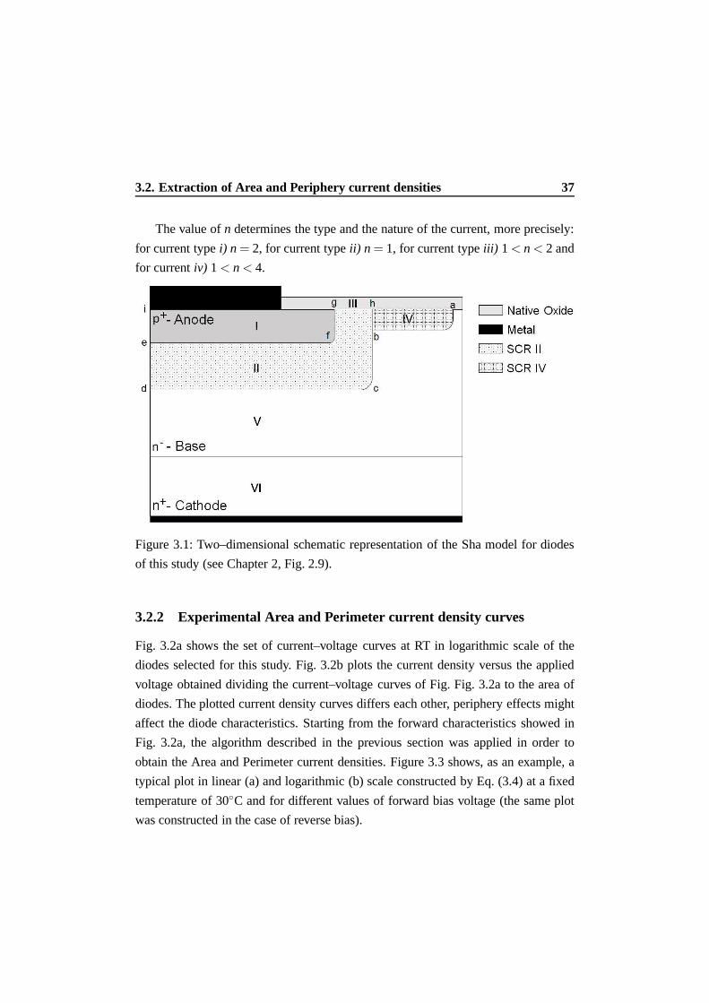
For the identification of the current type, the model proposed by Sah et al. [58][59]
for planar diodes with cylindrical symmetry (this suits thecase of ion implanted
diodes, Fig. 2.9) is considered. In this model, the diode total current is the sum of
four contributions:
i) a bulk recombination-generation current in the space charge region (SCR) of
the p-n junction that extends at the interface between emitter and base regions
(Fig. 3.1, SCR II, segment e–f–g). This interface is the sum of the emitter area
plus the emitter lateral surface (Fig. 3.1, SCR II, polygon h–c–d–e–f–g);
ii) a bulk diffusion current in the quasi neutral regions of the emitter volume and
surrounding diode base (Fig. 3.1, region V);
iii) a surface recombination-generation current in the region where the p-n junction
intercepts the wafer surface (Fig. 3.1, region III, region g–h);
iv) a bulk recombination-generation current in a channel that may form at the sam-
ple surface next to the Space Charge Region (SCR II, Fig. 3.1)because of the
native oxide/SiC interface charges (Fig. 3.1, SCR IV, delimited by the polygon
a–b–h).
The first two currents depend on the volume of devices, therefore from the area cur-
rent densityJarea(V,T ) in Eq. (3.3). The other two depend on the periphery of devices
and may be linked to the perimeter current densityJper(V,T ) in Eq. (3.3). All these
current components have an exponential dependence on V, so that forV greater than
few kT/q can be written as:
I(V,T ) = I0 ·
(
expqVnkT
)
(3.5)
whereI0 is the saturation or zero-voltage current that is dependenton the current type,
q is the electron elementary charge,V the applied voltage,k the Boltzmann constant,
T the absolute temperature andn the ideality factor.
Page 51
3.2. Extraction of Area and Periphery current densities 37
The value ofn determines the type and the nature of the current, more precisely:
for current typei) n = 2, for current typeii) n = 1, for current typeiii) 1< n < 2 and
for currentiv) 1< n < 4.
Figure 3.1: Two–dimensional schematic representation of the Sha model for diodes
of this study (see Chapter 2, Fig. 2.9).
3.2.2 Experimental Area and Perimeter current density curves
Fig. 3.2a shows the set of current–voltage curves at RT in logarithmic scale of the
diodes selected for this study. Fig. 3.2b plots the current density versus the applied
voltage obtained dividing the current–voltage curves of Fig. Fig. 3.2a to the area of
diodes. The plotted current density curves differs each other, periphery effects might
affect the diode characteristics. Starting from the forward characteristics showed in
Fig. 3.2a, the algorithm described in the previous section was applied in order to
obtain the Area and Perimeter current densities. Figure 3.3shows, as an example, a
typical plot in linear (a) and logarithmic (b) scale constructed by Eq. (3.4) at a fixed
temperature of 30C and for different values of forward bias voltage (the same plot
was constructed in the case of reverse bias).
Page 52
38 Chapter 3. Analysis of Static current–voltage curves
1.2 1.6 2.0 2.4 2.810-13
10-10
10-7
10-4
10-1
1000 m
curre
nt (
A )
voltage ( V )
150 m
@RT
(a)
1.6 2.0 2.4 2.810-10
10-7
10-4
10-1
102
curre
nt d
ensi
ty (
A / c
m2 )
voltage ( V )
1000 m
@RT
150 m
(b)
Figure 3.2: (a) Current–voltage characteristics at RT for all diodes of this study. (b)
The curves showed in (a) are divided by the anode area for obtaining the correspond-
ing current densities.
0 100 200 300
0.00
0.01
0.02
0.03
0.04
0.05
0.06
0.07
0.08
0 100 200 300
10-9
10-7
10-5
10-3
10-1
3.9V
1.71V
I/A (
A/cm
2 )
P/A ( cm-1 )
30°C - Linear
(a) (b)
3.9V30°C - Log
1.71V
Figure 3.3: Experimental current data divided by the emitter area of the studied diodes
and plotted versus the ratio 2/r by using Eq. (3.4) at 30C in linear (a) and logarithmic
scale (b).
Page 53
3.2. Extraction of Area and Periphery current densities 39
For each studied temperature, the starting voltage for the data analysis (1.71V at
30C, in Fig.3.3) is determined from the lowest common voltage among the whole
set of diodes which ensures a conduction current higher thanthe instrumental current
floor.
As clearly shown in Fig. 3.3(b) the slope of the curves decreases with increasing
voltages, meaning that the perimeter current is higher at low voltages and decreases
for increasing voltages.
Figure 3.4 features the core data of this study in the case of forward bias. In partic-
ular, (a) the perimeter (JF,Per) and (b) the area (JF,Vol) current density, obtained from
the intercept and the slope of curves in Fig. 3.3, respectively, are plotted as a function
of the applied voltage for different temperatures of measurement in logarithmic scale.
0 1 2 3 40 1 2 3 410-12
10-10
10-8
10-6
10-4
10-2
100 ( b )
J F,Vo
l ( A
/cm
2 ), J
F,Pe
r ( A
/cm
)
forward voltage ( V )
JF,Per 30°C 100°C 200°C 290°C
JF,Vol 30°C 100°C 200°C 290°C
( a )
Figure 3.4: Experimental perimeter (a) and area (b) currentdensities plotted versus
the applied voltage for several temperatures.
In Figure 3.5 the trend of the ideality factor, computed by using Eq. (2.2), of the
perimeter (a) and area (b) current densities is illustratedas a function of forward bias.
Page 54
40 Chapter 3. Analysis of Static current–voltage curves
These figures show that at low voltages and at all temperatures both the area and
perimeter current densities have an exponential trend witha value ofn around 2 and
that for increasing voltages 1<n<2 never passing through 1 before entering the ohmic
region.
1 2 31.0
1.5
2.0
nperimeter
30°C 100 200 290
Idea
lity
Fact
or
forward voltage ( V )
(a)
1 2 31.0
1.5
2.0
narea
30°C 100 200 290
Idea
lity
Fact
or
forward voltage ( V )
(b)
Figure 3.5: Trend of the ideality factorn for the perimeter (a) and the area (b) current
density.
A check like that for forward characteristics (Fig. 3.2), was performed for the re-
verse curves of the selected diodes. In particular, Fig. 3.6a shows the reverse current
curves at RT in logarithmic scale of the diodes and Fig. 3.6b show the correspond-
ing reverse current densities. This might mean that periphery effect might affect the
measured reverse diode characteristics.
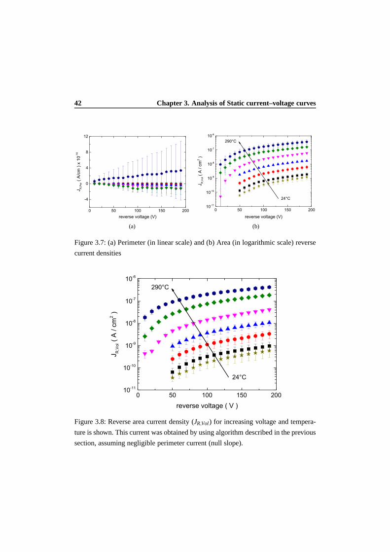
In Figure 3.7 are displayed (a) the Perimeter (JR,Per) and (b) Area (JR,Vol) current
densities, in the case of reverse bias: they are extracted byusing the same algorithm
used for forward bias (see, as an example Fig. 3.3) and described in the previous
section.
For small diameter diodes and for lower bias voltages, the measured reverse cur-
rent was comparable with the instrumental detection limit (as detailed in Chapter 2,
Section 2.5.2, Fig. 2.13). Therefore, in the temperature range from 24C up to 150C,
the obtained Area and Perimeter current density curves in Fig. 3.4 start at the reverse
Page 55
3.2. Extraction of Area and Periphery current densities 41
0 50 100 150 20010-15
10-14
10-13
10-12
10-11
reve
rse
curre
nt (
A )
reverse voltage ( V )
@RT
150 m 400 m 600 m
(a)
0 50 100 150 200
10-12
10-11
10-10
10-9
reve
rse
curre
nt d
ensi
ty (
A / c
m2 )
reverse voltage ( V )
150 m 400 m 600 m
@RT
(b)
Figure 3.6: (a) Reverse current–voltage curves at RT for alldiodes of this study. (b)
The curves showed in (a) were divided to the anode area for obtaining reverse current
densities.
voltage of 50V . For higher temperatures, over 150C, the value of reverse current was
sufficiently high to be detected even at low voltages.
The reverse perimeter current density is scattered and has not a well defined trend
dependence on the temperature and voltage and its value is always lower than the area
current density. Therefore, it was assumed that the reversecurrent of these devices
can mainly linked to their volume. For this reason the fittingof curves like those
showed in Fig. 3.3 was performed by assuming null slope: the obtained results are
shown in Fig. 3.8. The Affinity between absolute current values in the latter figure and
those showed in Fig. 3.7b, confirm that the contribution of perimeter reverse current
density can be neglected and therefore the reverse current density of these devices
can be linked to their volume.
Page 56
42 Chapter 3. Analysis of Static current–voltage curves
0 50 100 150 200
-4
0
4
8
12
J R,P
er (
A/cm
) x
10-1
0
reverse voltage (V)
(a)
0 50 100 150 20010-11
10-10
10-9
10-8
10-7
10-6
J R,V
ol (
A / c
m2 )
reverse voltage (V)
24°C
290°C
(b)
Figure 3.7: (a) Perimeter (in linear scale) and (b) Area (in logarithmic scale) reverse
current densities
0 50 100 150 20010-11
10-10
10-9
10-8
10-7
10-6
J R,V
ol (
A / c
m2 )
reverse voltage ( V )
24°C
290°C
Figure 3.8: Reverse area current density (JR,Vol) for increasing voltage and tempera-
ture is shown. This current was obtained by using algorithm described in the previous
section, assuming negligible perimeter current (null slope).
Page 57
3.3. Current temperature dependences and Arrhenius plot 43
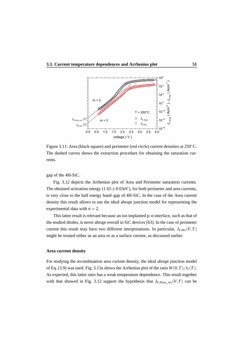
3.3 Current temperature dependences and Arrhenius plot
3.3.1 Theoretical background II
Area current density
The forward area current densityJF,Area (Jarea in Eq. 3.3), in the ideal case of a semi–
infinite bipolar junction, is the sum of a recombination (JF,Area_rec) and diffusion
(JF,Area_di f f ) currents, as described in the Sah model, in particular:
JF,Area(V,T ) = JF,Area_rec(V,T )+ JF,Area_di f f (V,T ) (3.6)
The two terms of Eq. (3.6) can be expressed as [45]:
JF,Area_rec(V,T ) =qW (V,T )ni(T )
2τr(T )· exp
(
qV2kT
)
(3.7)
JF,Area_di f f (V,T ) = q
√
Dp(T )τp(T )
·n2
i (T )ND
· exp
(
qVkT
)
(3.8)
whereq is the electron charge,W is the depletion region width,ni is the intrinsic
carrier concentration,τr is the effective carrier recombination lifetime in the Space–
Charge Region (SCR),k is the Boltzmann constant,Dp andτp are the minority carrier
diffusion coefficient and lifetime, respectively, andND is the ionized donor concen-
tration in the diffusion region. Dependences on the absolute temperatureT and on
the applied voltageV of all variables in Eqs. (3.7) and (3.8) are specified inside the
round brackets.
An accurate study of pre–exponential factors, or saturation zero-voltage currents,
in Eqs. (3.7) and (3.8) is remarkable since these currents are linked to the material
parameters, in particular:τr and the ratioDp/τp.
The temperature dependences of the pre–exponential factors of the above equa-
tions can be studied by extrapolating to zero–voltage the relative current component,
therefore:
JF0,Area_rec(0,T ) =qW (0,T )ni(T )
2τr(T )(3.9)
Page 58
44 Chapter 3. Analysis of Static current–voltage curves
JF0,Area_di f f (0,T ) = q
√
Dp(T )
τp(T )·
n2i (T )ND
(3.10)
where in above equations the intrinsic carrier density can be expressed as [45]:
ni(T ) =√
NC(T ) ·NV(T ) · exp
(
−Eg(T )2kT
)
(3.11)
In Eq. (3.11)NC(T ) andNV (T ) are the temperauture–dependent effective density of
state in the conduction and valence band, respectively andEg(T ) is the temperature
dependent band–gap. These quantities can be expressed as [45]:
NC(T ) = 2·
(
2πmdekTh2
)3/2
·Mc (3.12)
NV (T ) = 2·
(
2πmdhkTh2
)3/2
(3.13)
Eg(T ) = Eg(4K)−αT 2
(β +T)(3.14)
where in Eqs. (3.12) and (3.13)mde andmdh are the density of state effective mass
for electrons and holes, respectively,h is the Planck constant, in Eq. (3.12)Mc is the
number of equivalent minima in the conduction band. In Eq. (3.14) Eg(4K) is the
value of the energy gap at 4K,α andβ are two fitting parameters.
Under the hypothesis of abrupt junction, assumingNA >> ND (with NA andND
are the net acceptors and donors densities, respectively),the depletion layer width
W (V,T ) in Eq. (3.7) can be expressed as [45]:
W (V,T ) =
√
2ε0εr
qND· (Vbi(T )−V ) (3.15)
whereε0 is the vacuum dielectric constant,εr is the relative material dielectric con-
stant,V the applied voltage andVbi is the temperature dependent built–in potential
given by [45]:
Vbi =kTq
ln
(
NA(T )ND
n2i
)
(3.16)
Page 59
3.3. Current temperature dependences and Arrhenius plot 45
whereq, k, T , ND andni were defined earlier, andNA is the temperature dependent
acceptors density in the anode equal to the activated implantedAl density.
Assuming a weak temperature dependence of the ratioW (0,T )/τr(T ) it follows
that the main temperature dependence ofJF0,Area_rec of Eq. (3.9) is:
JF0,Area_rec(0,T ) ∝ ni(T )
∝√
T 3/2 ·T 3/2 · exp
(
−Eg(T )2kT
)
∝ T 3/2exp
(
−Eg(T )
2kT
)
hence:
JF0,Area_rec(0,T ) / T 3/2 ∝ exp
(
−Eg(T )
2kT
)
ln(
JF0,Area_rec(0,T ) / T 3/2)
∝ −1
2kT·Eg(T ) (3.17)
Therefore in the frame of this ideal abrupt junction model for the recombination
current, making a plot of the natural logarithm of the ratio(JF0,Area_rec(0,T ) / T 3/2)
versus 1/2kT and fitting the curve with a straight line, its slope gives thematerial
energy gap. It means that to apply this model and to extract a reliable value of the
recombination lifetimeτr within the Space Charge Region (SCR), the slope obtained
by linear fitting the plot of experimental data constructed by Eq. (3.17), must verify
the above described condition, that is, must give the material energy gap.
The same reasoning applies toJF0,Area_di f f (0,T ). In particular, starting from Eq.
(3.10), assuming that√
Dp
τpis proportional toT γ/2 whereγ is constant [45], the tem-
perature dependence ofJF0,Area_di f f (0,T ) can be written as:
JF0,Area_di f f (0,T ) ∝ T γ/2 ·
[
T 3/2 · exp
(
−Eg(T )2kT
)]2
∝ T γ/2 ·T 3 · exp
(
−Eg(T )
kT
)
JF0,Area_di f f (0,T ) / T 3 ∝ T γ/2 · exp
(
−Eg(T )
kT
)
(3.18)
Page 60
46 Chapter 3. Analysis of Static current–voltage curves
Since the termT γ/2 is weak compared to the exponential one, Eq. (3.18) can be
rewritten as:
JF0,Area_di f f (0,T ) / T 3 ∝ exp
(
−Eg(T )
kT
)
and hence:
ln(
JF0,Area_di f f (0,T ) / T 3) ∝ −1
kT·Eg(T ) (3.19)
As discussed earlier forJF0,Area_rec, before applying this model to the diffusion
current, the Arrhenius plot of experimental data must return the material energy gap.
Perimeter current density
As the diode emitters of this study have been doped by a selective area ion implanta-
tion process (see Chapter 2 for further details), a lateral bipolar junction surrounding
the emitter over its thickness is present. This junction maycontribute to the perimeter
current component with a recombination and a diffusion current governed by Eqs.
(3.7) and (3.8).
At the same time, this p–n junction crosses orthogonally thewafer surface (as
shown in Fig. 3.1, region g–h), therefore perimeter current, governed by surface cur-
rent, may be expected. This latter have an exponential-likedependence which can be
modelled as [54][60]:
JF,Per(V,T ) = qsp(T )Ls(T )ni(T ) · exp
(
−qV2kT
)
(3.20)
wheresp(T ) is the surface recombination velocity andLs(T ) is the surface diffusion
length, both of these variables are dependent on the temperature (T ). Extrapolating
to zero-voltage the previous equation it follows:
JF0,Per(0,T ) = qsp(T )Ls(T )ni(T ) (3.21)
A weak temperature dependence of the productsp(T )Ls(T ) is expected, therefore the
temperature dependence of the perimeter saturation current is determined by that of
Page 61
3.3. Current temperature dependences and Arrhenius plot 47
the intrinsic carrier density:
JF0,Per(0,T ) ∝ ni(T )
∝ T 3/2 · exp
(
−Eg(T )
2kT
)
and hence:
JF0,Per(0,T ) / T 3/2 ∝ exp
(
−Eg(T )
2kT
)
ln(
JF0,Per(0,T ) / T 3/2)
∝ −1
2kT·Eg(T ) (3.22)
As discussed earlier for the area current density, making anArrhenius plot of ex-
perimental data by using Eq. (3.22) if the resulting curve isa straight line with a
slope equal to the material energy gap, reliable values of the productspLs, which is
considered as a quality factor of surface passivation, can be obtained from Eq. (3.21).
Reverse area current
The reverse area current densityJR,Area(V,T ), as in the forward case, can be expressed
as a sum of generation and diffusion currents [45]:
JR,Area(V,T ) = JR,Area_gen + JR,Area_di f f (3.23)
where in Eq. (3.23):
JR,Area_gen(V,T ) =qW (V,T )ni(T )
τg(T )(3.24)
JR,Area_di f f (V,T ) = q
√
Dp(T )
τp(T )·
n2i (T )
ND(3.25)
in Eq. (3.24)τg(T ) is the generation lifetime of carriers within the SCR, the other
variables in Eqs. (3.24) and (3.25) were previously defined.
In the case of semiconductor with small values of intrinsic carrier densityni(T )
(such as Silicon Carbide) the diffusion current component will be necessarily negli-
gible compared to the generation one, therefore:
JR,Area(V,T )≈ JR,Area_gen(V,T )≈qW (V,T )ni(T )
τg(T )(3.26)
Page 62
48 Chapter 3. Analysis of Static current–voltage curves
Under the hypothesis of abrupt junction (as supposed so far), the depletion layer
width W (V,T ) can be expressed by using Eq. (3.15) obtaining:
JR,Area_gen(V,T )≈qni(T )τg(T )
·
√
2ε0εr
qND· (Vbi(T )−V ) (3.27)
This equation shows that this ideal model can be used for representing the experi-
mental data only if:
JR,Area_gen(V,T ) ∝ V 1/2 (3.28)
3.3.2 Calculated constant values
The constant values, used for the calculation of described variables in the previous
section, are reported in Table 3.1.
In this studyND is equal to theN− donor density of the epitaxial layer, as this
concentration is low (3×1015cm−3) even at Room Temperature all donors are fully
ionized, as shown, as an example, in Fig. 3.9 for 6H–SiC.
Figure 3.9: Example of dopants partial ionization at different temperatures in the case
of 6H–SiC material.
Page 63
3.3. Current temperature dependences and Arrhenius plot 49
The hole densityNA(T ) in the anode is a function of temperature and is plotted in
Fig. 3.10. This latter figure was obtained from literature data of Hall-effect measure-
ments for the same implantation process and electrical activation thermal treatment
of the studied diodes [49].
Figure 3.10: Experimental hole density as a function of temperature.
3.3.3 Data analysis and experimental results
Figure 3.11 depicts, as an example, the area (black square) and perimeter (red circle)
current densities at a fixed temperature of 250C. The black and red dashed lines
represent the extrapolation to zero–voltage of the area andperimeter current density
curves, respectively, with ideality factorn = 2.
This extrapolation procedure was applied to all curves at all temperatures. The so
obtained set of recombination saturation currents (JF0,Area_rec(0,T ) andJF0,Per(0,T ))
were studied following the methodology discussed in Section 3.3.1 for the area and
perimeter currents. In particular, for applying the abruptjunction model, the Arrhe-
nius plot of the saturation currents of the curve trait withn = 2 must give the energy
Page 64
50 Chapter 3. Analysis of Static current–voltage curves
PHYSICAL CONSTANTS
Parameter Symbol Value Ref.
Electron charge q 1.602×10⁻¹⁹ [C] [45]
Electron rest mass m0 9.1095×10⁻³¹ [kg]
Boltzmann constant k 1.381×10⁻²³ [J/K]
8.617×10⁻⁵ [eV/K]
Permittivity in vacuum ε0 8.854×10⁻¹⁴ [F/cm]
Plank constant h 6.626×10⁻³⁴ [J s]
4.136×10⁻¹⁵ [eV s]
PROPERTIES OF4H-SIC
Conduction Band Minima Mc 3 – [61]
Energy Gap (4K) Eg(4K) 3.265 [K]
α α 6.5×10⁻⁴ [eV/K]
β β 1.3×10³ [K]
Dielectric constant εr/ε0 9.66 –
eDOS Mass mde/m0 0.42 – [62]
hDOS Mass mdh/m0 2.6 –
Table 3.1: Physical constant and 4H-SiC material properties used in calculations.
Page 65
3.3. Current temperature dependences and Arrhenius plot 51
0.0 0.5 1.0 1.5 2.0 2.5 3.0 3.5 4.010-16
10-13
10-10
10-7
10-4
10-1
102
JF0,Per (T)m = 2 JF,Area
JF,Per
voltage ( V )
T = 250°C
m = 2
JF0,Area_rec (T)
J F,Ar
ea (
Acm
-2 ),
JF,
Per (
Acm
-1 )
Figure 3.11: Area (black square) and perimeter (red circle)current densities at 250C.
The dashed curves shows the extraction procedure for obtaining the saturation cur-
rents.
gap of the 4H-SiC.
Fig. 3.12 depicts the Arrhenius plot of Area and Perimeter saturation currents.
The obtained activation energy (1.65±0.03eV ), for both perimeter and area currents,
is very close to the half energy band–gap of 4H-SiC. In the case of the Area current
density this result allows to use the ideal abrupt junction model for representing the
experimental data withn = 2.
This latter result is relevant because an ion implanted p–n interface, such as that of
the studied diodes, is never abrupt overall in SiC devices [63]. In the case of perimeter
current this result may have two different interpretations. In particular,JF,Per(V,T )
might be treated either as an area or as a surface current, as discussed earlier.
Area current density
For studying the recombination area current density, the ideal abrupt junction model
of Eq. (3.9) was used. Fig. 3.13a shows the Arrhenius plot of the ratioW (0,T )/τr(T ).
As expected, this latter ratio has a weak temperature dependence. This result together
with that showed in Fig. 3.12 support the hypothesis thatJF,Area_rec(V,T ) can be
Page 66
52 Chapter 3. Analysis of Static current–voltage curves
15 30 45-80
-60
-40
-20
(1.65 + 0.03) eV
ln (
J F0_B
_rec
/ T
3/2 )
B = Area, Per Area Per
q/kT (eV-1)
Figure 3.12: Arrhenius plot of Area (black triangles) and Perimeter (red circle) satu-
ration current densities.
20 25 30 35 4040
80
120
160
200
W(0
,T) /
r(T
)
q / kT ( eV -1 )
(a)
0 50 100 150 200 250 3000.0
0.5
1.0
1.5
2.0
r (
s )
T (°C)(b)
Figure 3.13: (a) Temperature dependence of the ratio between the space charge re-
gion at zero saturation voltage (W (0,T ))and the recombination lifetime (τr(T )). (b)
Recombination lifetime vs temperature.
Page 67
3.3. Current temperature dependences and Arrhenius plot 53
modelled as a recombination current.
Fig. 3.13b shows the estimated recombination lifetimeτr within the SCR versus
the temperature. The computed values are of the order of about 1.1µs.
A curve trait withn = 1 may be found before ohmic regime, if the bulk diffu-
sion current becomes dominant on the recombination one. When this condition in
not fulfilled the ideality factorn has a value between 1 and 2 [45]. In this latter case,
0.0 0.5 1.0 1.5 2.010-20
10-16
10-12
10-8
10-4
100
m = 1
JF0,Area_diff (T)
JF0,Area_rec (T)
J F,Ar
ea (
Acm
-2 )
T = 250°C
JF,Area JF,Area_rec JF,Area - JF,Area_rec
voltage ( V )
m = 2
Figure 3.14: Graphical procedure for obtaining the diffusion current. The area recom-
bination current desnity (red circle) is subtracted from the total area current density
(black square) and the diffusion current density (blue triangle) is obtained.
diffusion and recombination currents might be comparable and the trait of curve with
n = 1 might be recognized by using a graphical approach. Fig. 3.14, as an exam-
ple, shows the graphical procedure for isolating the diffusion current component. In
particular, by extrapolating the recombination current tohigher voltages (red open
circles in Fig. 3.14), by using Eq. (3.7), and subtracting itfrom the total Area current
density (black open squares in Fig. 3.14), the diffusion componentJF,Area_di f f (V,T )
was obtained (blue open triangles in Fig. 3.14). As shown in the figure, at low volt-
ages the current withn = 2 due to the recombination within the SCR controls the
curve. At higher voltages the diffusion current is significant for a limited voltage
Page 68
54 Chapter 3. Analysis of Static current–voltage curves
ranges before the ohmic conduction starts dominating the last part of the curve. By
this procedure a set of diffusion saturation currentJF0,Area_di f f (0,T ) was obtained
for each temperature.
In figure 3.15, the Arrhenius plot of the so obtained diffusion saturation currents,
is depicted. The extracted activation energy of 2.77±0.04eV is too far from the en-
20 25 30 35 40-120
-100
-80
-60
-40
ln J
F0,A
rea_
diff /
T3
q/KT (eV-1)
( 2.77 + 0.04 ) eV
Figure 3.15: Arrhenius plot of the diffusion current component.
ergy band–gap of 4H-SiC to conclude that the exponential dependence in Eq. (3.17)
is dominant. This rules out the possibility to use Eq. (3.10)for an estimation of the
minority carrier lifetimeτp in the drift layer. Even if the ideal abrupt junction model
cannot be applied to all current components, the separationof perimeter and area
current densities has allowed to observe that traits of the forward current of 4H-SiC
p+− i−n− diodes can be described as the sum of two exponential currentcontribu-
tions with ideality factorn = 2 andn = 1, plus the ohmic region contribution.
Perimeter current density
As observed earlier, the result shown in Fig. 3.12 may have two interpretations. In
particular the perimeter component may be treated as:
Page 69
3.3. Current temperature dependences and Arrhenius plot 55
• an area current and studied by using the equations Eqs. (3.7) and (3.8);
• a perimeter current and studied by using Eq. (3.20).
In the first case the evaluation ofτr(T ) requires the knowledge of the lateral exten-
sion width of the SCR region adjacent to the emitter perimeter (i.e. the length of the
segment a–h relative to SCR IV in Fig. 3.1). Since it was not possible to estimate
it, the hypothesis of modelling the perimeter current by using Eq. (3.7) was not con-
sidered. Moreover, applying the graphical procedure showed in Fig. 3.14, the trait
with ideality factorn = 1 was not observed. For this two reasons,JF,Per(V,T ) in this
study was treated as a surface current and the surface quality factor (i.e. the product
sp(T )Ls(T )) was calculated.
Fig. 3.16 represents the productsp(T )Ls(T ) as a function of temperature. It can be
0 100 200 3000.0
0.5
1.0
1.5
2.0
2.5
s pLs (
cm
2 s-1 )
T (°C)
Figure 3.16:sp(T )Ls(T ) quality factor vs temperature. The dashed line represents the
average value.
state that, as expected, the temperature dependence is weak. The value of the product
sp(T )Ls(T ) is often used for qualifying the surface passivation, more precisely lower
values of this product imply better surface passivations. Since the diodes of this study
have no intentional surface passivation, the curve of Fig. 3.16 qualifies the passivation
due to the native oxide, or oxy-carbide, that spontaneouslyforms on the 4H-SiC wafer
surface when it is exposed to air. These values are two order of magnitude lower than
Page 70
56 Chapter 3. Analysis of Static current–voltage curves
those published for mesa 4H-SiC p–i–n diodes [54]. This is promising for the use of
selected area ion implantation technology for the fabrication of SiC bipolar junctions.
Reverse current density
Unfortunately, the reverse area current densities showed in Fig. 3.8 have aV –dependence
steeper than theV 1/2 expected in case of a pure generation current and therefore
the simple model of abrupt junction cannot be used for representing the experimen-
tal data. Nevertheless, under the hypothesis that this current might be dominated by
carrier emission from traps within the depleted region, thetemperature dependence
might be determined by the trap emission rate [64]:
JR,Area(V,T ) ∝ T 2exp
(
−Ena
kT
)
(3.29)
whereEna is a trap signature. Passing through the natural logarithm it follows that:
ln(
JR,Area(V,T )/T 2) ∝−Ena
kT(3.30)
Fig. 3.17 shows the Arrhenius plot ofJR,Area(V,T )/T 2 for V = −100,−190V .
Within errors, the two curves can be fitted by activation energies of 0.20+0.02eV at
low T and of 0.49+0.06eV at highT .
As the two reverse bias values show identical trap signatures, the hypothesis that
trap distribution over the depleted depth is uniform may hold. The trap signature of
Eq. 3.29 is connected with but does not exactly corresponds to the trap energy po-
sition in the band gap. In order to validate this extraction procedureEna has been
compared with the trap signature obtained by other electrical characterization tech-
niques, such as deep level transient spectroscopy (DLTS).
The electrically active defects in diodes of this study havebeen identified by
DLTS and the results are reported in [43]. Three electron traps were found, in partic-
ular: EH6/7 at(Ec−1.5)eV , Z1/2 at(Ec−0.67)eV , andX1 at(Ec−0.16)eV , plus
a hole trapX2 at(Ev−0.35)eV .
Z1/2 andEH6/7 are traps associated with the presence of carbon vacanciesVC
while X1 is systematically present in n–type 4H-SiC and may be due tometal impuri-
Page 71
3.4. Numerical simulations 57
20 24 28 32 36 40-36
-32
-28
-24
(0.20 + 0.02) eV
(0.20 + 0.02) eV
(0.47 + 0.04) eVln (
J R,A
rea_
V / T
2 )
q/kT ( eV-1 )
ln ( JR,Area_100V / T2 ) ln ( JR,Area_190V / T2 ) (0.50 + 0.06) eV
Figure 3.17: Arrhenius plot of the reverse area current density at two different bias
voltage:−100V (black full circle) and−190V (black open circle).
ties [65]. The high density ofVC defects in the drift layer of diodes of this study is due
to the very high temperature of the post–implantation annealing process [43][66][67].
The trap signatures showed in Fig. 3.17 and those ofZ1/2 andX1 defects iden-
tified by DLTS are in good agreement, while the very deep trap responsible of the
recombination current is likely to be theEH6/7 trap [68][69], and it was observed in
forward study (Fig. 3.12).
3.4 Numerical simulations
3.4.1 Motivations
Numerical simulation of forward characteristics of the studied diodes has been per-
formed by using Synopsys Sentaurus TCAD [70] with the aim to explain the origin
of perimeter current.
The experimental activation energies, obtained from forward and reverse curve
analysis (see Section 3.3), were used and their effect on thearea and perimeter current
Page 72
58 Chapter 3. Analysis of Static current–voltage curves
components was also studied.
Since, the previous performed analysis of experimental current–voltage curves
gives only the distance of defects within the band–gap from one of the edge band,
for classifying defects in terms of capture cross section, defect densities and type, the
support of other measurement techniques is needed. Therefore, Deep Level Transient
Spectroscopy (DLTS) measurements [43] were also performedon the studied diodes
as already reported at the end of the previous Section. Theseresults are in agreement
with those present in literature for other ion implanted 4H–SiC devices. Therefore,
the available capture cross sections and defect densities of DLTS study were used as
input parameters within Sentaurus TCAD. The missing information can be consid-
ered as an original results used for fitting the area and perimeter forward curves of
the studied 4H–SiC devices.
This procedure, which involves detailed electrical measurements and data analy-
sis, combined with appropriate literature results (for obtaining the missing informa-
tion from the electrical curves analysis), allows, in first approximation, the creation
of models which may be used to explain not considered effectsspeeding up and im-
proving design and fabrication of new devices.
3.4.2 Used models and simulation parameters
Simulations are based on the solution of well–known stationary drift–diffusion equa-
tions including models for incomplete ionization of dopants [71] and band–gap nar-
rowing [72]. Physically based models for Shockley-Read-Hall (SRH) and Auger [73]
recombination are used as well, even if, under the operatingconditions of interest,
SRH recombination is dominant and Auger recombination negligible.
Electron and holes mobilities are modelled by the empiricalrelation of Caughey–
Thomas with the fitting parameters for SiC taken from [74]. All simulations have
been performed at Room Temperature (RT). The fundamental 4H–SiC parameters
used in all simulations are listed in Table 3.2.
The cylindrical symmetry of the diodes (see Fig. 3.18) allows limiting the sim-
ulated area to half of the cross–section on a symmetry plane and calculating the 3D
current in a post–processing step thanks to the cylindricaloption available in Syn-
Page 73
3.4. Numerical simulations 59
opsys tool [70]. The modelled structure is the section inside the black frame in Fig.
3.18.
Figure 3.18: 3D cross–section of simulated diodes.
While then− andn+ regions have a constant doping of 3×1015cm−3 (see Chap-
ters 2 and 3 for details) and 7× 1018cm−3 (corresponding to 0.021Ωcm resistivity)
respectively, the anode acceptor doping is variable with depth. Fig. 3.19 shows the
Al+ acceptor depth profile with the corresponding hole distribution at RT; the former
has been computed taking into account the implanted Al depthprofile simulated by
SRIM2008 [30] and an electrical activation of 80%, the latter by Synopsys-Sentaurus
TCAD, which accounts for the temperature dependence of the partial ionization of
the Al acceptors in 4H–SiC. In the light of the net donor density in the n–epilayer,
the metallurgic p–n junction of diodes of this study falls ata depth of about 0.85µm.
3.4.3 Simulation results
Area current density
In order to obtain the area current density, the ideal devicewith Lma +Lmda section
(Fig. 3.18) was simulated and the effect of single traps on the electrical characteristics
were studied. As explained in the introduction, type and density of defects used in
the SRH model are based on DLTS study, while the used trap activation energiesEA1,
Page 74
60 Chapter 3. Analysis of Static current–voltage curves
4H-SIC SIMULATION PARAMETERS AT T0 = 300K
Parameter Symbol Value Ref.
Energy gap Eg 3.2 [eV] [45]
Electron affinity χ 4.1 [eV]
Dielectric constant εr/ε0 9.66 –
eDOS Mass mde/m0 0.42 – [62]
hDOS Mass mdh/m0 2.6 –
DOPANT INCOMPLETE IONIZATION: MAXIMUM IONIZATION ENETRGY
Aluminum Al 0.265 [eV] [71]
Nitrogen N 0.05 [eV] [75]
CAUGHEY–THOMAS MODEL FOR MOBILITY DOPING DEPENDENCE
electron hole
µmax 954 120 [cm2/Vs] [74]
µmin 0 15.9 [cm2/Vs]
Nre f ×1017 1.28 18 [cm−3]
a 0.61 0.65 –
Table 3.2: Simulation parameters used for modelling 4H-SiCmaterial.
Page 75
3.4. Numerical simulations 61
0.0 0.2 0.4 0.6 0.8 1.01016
1017
1018
1019
1020
1021
Con
cent
ratio
n ( c
m-3 )
Active Al Doping Hole
Depth ( m )
Figure 3.19: Active implanted Aluminum density versus depth obtained as the 80%
of SRIM2008 simulated profile (dark solid line), emitter hole concentration versus
depth simulated by Synopsys-Sentaurus TCAD (dashed red line).
EA2 andEA3 were those extracted from the experimental data analysis showed in the
previous chapter. Table 3.3 summarize trap properties usedin simulations.
DEFECT PROPERTIES
Defect Position type τe τh
[eV] [ns] [ns]
L1 EC −1.65 donor 12 20
L2 EC −0.2 acceptor 420 10
L3 EC −0.5 acceptor 8 100
thermal velocity, vth - electrons: 1.9×107cm/s, holes: 1.2×107cm/s
Table 3.3: Defect properties used in simulations.
Fig. 3.20 shows simulation results, in particular: the solid line is the simulation
which takes into account all traps, the dotted line is the simulation without traps
and the other dashed lines are simulations with single traps. The experimental area
current density (see section 3.2) is represented with open symbols. This graph shows
Page 76
62 Chapter 3. Analysis of Static current–voltage curves
the effect on the total current of each single trap.
1.8 2.1 2.4 2.7 3.0 3.310-11
10-9
10-7
10-5
10-3
10-1
101
J F,Ar
ea_s
im (
A/cm
2 )
Voltage (V)
ExperimentalSimulations:
no traps L1 L2 L3 all traps
Figure 3.20: Open black squares represent the experimentaldata, black solid line
show the simulated area current density taking into accountall traps, while the black
dot line show the ideal area current density (no traps). The other curves represent the
contribution to the total simulated area current density ofthe single traps listed in
table 3.3.
The level L1 can be identified withEH6/7 defect that originates from a car-
bon vacancy [76][77]. In the proposed model this defect is a donor, uniformly dis-
tributed in the diode’s volume and positioned atEA1 = 1.65eV under the conduc-
tion band edge [68][43]. Its concentration, taken from DLTSmeasurements [43], is
NT1 = 2.4×1014cm−3. TheEH6/7 level controls the carrier lifetime in p–type 4H–
SiC [78] and therefore doping–concentration–dependent SRH carrier lifetime for this
defect is considered, which is calculated as:
τL1 =τ0
1+(
NAlNRe f
)γ (3.31)
whereNRe f = 5×1018cm−3, γ = 1.2 andNAl is the implanted Aluminum concentra-
Page 77
3.4. Numerical simulations 63
tion. As in [78] and [43],τ0 = 20ns is assumed for holes, while for electronsτ0 = 12ns
is based on DLTS data [43].
Level L2 has been tentatively attributed to a residual impurity of a transition
metal like Ti or Cr, commonly observed in 4H-SiC [65]. Traps located atEC−0.16eV
andEC −0.18eV are assigned to Ti [65][69], while a trap located atEC −0.17eV is
attributed to Ti or Cr [79]. However, this trap has an acceptor–like behaviour. The trap
concentration and electron capture cross section lie in theranges 1013− 1014cm−3
and 8×10⁻¹⁶−2×10⁻¹⁴cm2 [69][80][81], respectively. Referring to the DLTS data
[43], concentrationNT2 = 4.2× 1013cm−3 and electron capture cross sectionσe =
3×10⁻¹⁵cm2 were fixed, while hole capture cross–sectionσh = 2×10⁻¹³cm2 values
gave the best match between measurements and simulations.
The Level L3 located around at 0.50eV above the valence band maximum has
been observed by several groups and usually is identified as the Boron–related D–
center [82][83][84][85]. However, considering that the Boron–related D–center has
been mainly detected in p–type–grown or Boron–implanted devices, in this study it
has been attributed to theZ1/2 centre as commonly observed by DLTS measurement
on ion implanted diodes [2][3][43]. Therefore, the energy position of L3 is 0.5eV
below the conduction band. Its concentration and electron capture cross section are:
NT3 = 4.2×1014cm−3 andσe = 1.8×10⁻¹⁴cm2, respectively [43]. The correspond-
ing hole capture cross–section was fixed at 2×10⁻¹⁵cm2.
Perimeter current density
Taking into account all defects used in the previous section(listed in Table 3.3) for re-
producing the area current density, simulations on diodes with different diameter (as
listed in Table 3.4) were performed in order to explain the origin of the experimental
perimeter current density.
For taking into account the periphery of diodes, With respect to the previous ideal
simulation, theLma +Lmda +Lda section (Fig. 3.18) was considered.
Fig. 3.21 shows the simulated current of the Diode labelled as B (400µm diame-
ter, see Table 2.1), in particular, as already seen for the area current density, the solid
line is the simulation of the total current taking into account all traps, the dotted line
Page 78
64 Chapter 3. Analysis of Static current–voltage curves
is the simulation without traps and the other dashed lines are simulations with single
traps, while the experimental data are represented by open symbols.
SIMULATED DIODE CHARACTERISTICS
Diode Lma Lmda Lda RD_anode RD_cathode
[µm] [µm] [µm] [Ω] [Ω]
A 55 20 50 1.9×10⁻³ 10−4
B 175 25 50 7×10⁻³ 10−4
C 475 25 50 4.5×10⁻² 10−4
Table 3.4: Geometrical characteristics of the simulated diodes and distributed resis-
tanceRD_anode/cathode used for each diode.
1.8 2.1 2.4 2.7 3.0 3.310-15
10-12
10-9
10-6
10-3
100
voltage ( V )
curre
nt (
A )
Diode B Measurement
Simulations: no traps (ideal) L1
L2 L3
all traps
Figure 3.21: Simulation of the total current (black solid line) of the 400µm diameter
diode (Diode B). The black open symbols are the experimentaldata.
In the case of diode B (Fig. 3.21) the simulation match the experimental data.
Figs. 3.22 show the simulated total current for diodes A, B and C. No adjustment
of simulation parameters was made from sample to sample: only the geometry was
changed (see Tabele 3.4). The black dashed lines represent the simulated area current
Page 79
3.4. Numerical simulations 65
considering the sectionLma + Lmda, the red dot–dashed lines are the total current
without hypothesis on the surface next to the diode anode andconsidering the diode
periphery (sectionLma+Lmda+Lda, Fig. 3.18). Finally, the blue solid lines represents
the total simulated current obtained by using a model which accounts for periphery
effects. This model will be detailed later on.
In Figs. 3.22 two different regions, divided by the dashed line, can be recognized:
the region I at low voltages and the region II at high voltages.
In the case of larger diode C, the region II is completely controlled by the area
current. In particular, as shown in Fig. 3.22c, the area (black dashed line) and total
(red dot–dashed line) simulated currents overlap and both of them match the exper-
imental data (open black triangles). Always considering Region II, in the case of
diodes A and B, the only simulated area current (black dashedline) do not match
the experimental data, as shown in Fig. 3.22a and Fig. 3.22b.The presence of diode
periphery is necessary to reproduce the experimental data,indeed the total current,
represented by the red dot–dashed line, match the experimental data (open black
squares and circles). Furthermore, it is worth to highlightthat the difference between
the area simulated current (black dashed line) and the totalsimulated current (red
dot–dashed line) decreases with the increasing of diode dimensions.
Observing region I, the simulated area current (black dashed line) fits the total
simulated current (red dot–dashed line) for all diodes. Moreover, in diodes B and C
the simulated area current also reproduces the measured current (symbols) quite well,
whereas in diode A there are some discrepancies.
The fact that the simulated current at low voltages (region I) does not scale with
the diode dimension suggests that some effects on the periphery of diodes are not
accounted for in the simulation model. These effects are negligible in larger diameter
devices and are more relevant for smaller diodes, indeed thelow–voltage recombi-
nation current in the simulation for diode A is underestimated. This underestimation
may be due to some inaccuracy of the surface modelling. The studied diodes have no
intentional surface passivation but the presence of nativeoxide may be expected, as
supposed in the previous Section 3.3.
The presence of a native oxide was taken into account by placing a negative fixed
Page 80
66 Chapter 3. Analysis of Static current–voltage curves
1.8 2.1 2.4 2.7 3.0 3.3 3.610-15
10-12
10-9
10-6
10-3
100
MeasurementSimulations:
area current Diode A no surface fixed charge negative surface fixed charge
curre
nt (
A )
Voltage (V)
Diode A
( I ) ( II )
(a)
1.8 2.1 2.4 2.7 3.0 3.3 3.610-15
10-12
10-9
10-6
10-3
100
MeasurementSimulations:
area current Diode B no surface fixed charge negative surface fixed charge
curre
nt (
A )
Voltage (V)
Diode B
( I ) ( II )
(b)
1.8 2.1 2.4 2.7 3.0 3.3 3.610-15
10-12
10-9
10-6
10-3
100
( I ) ( II )
voltage ( V )
curre
nt (
A )
Diode C
MeasurementSimulations:
area current Diode C no surface fixed charge negative surface fixed charge
(c)
Figure 3.22: Simulation results for different diameter diodes, in particular: (a) small
diameter diode A, (b) medium diameter diode B, (c) large diameter diode C. This
figure shows that for smaller dimension diode the periphery is necessary to reproduce
the experimental data (blue solid line).
Page 81
3.4. Numerical simulations 67
charge of densityQ f ix on the diode surface [86][87] that extends over the distance
Lmda + Lda (Fig. 3.18 and Fig. 3.1 for comparison with the model of Sha).The in-
sertion ofQ f ix/q = −5×1012cm−2 increases the recombination current of diode A
at low voltages and the simulation match the experimental curve (as shown in Fig.
3.22a, solid blue line). On the other hand, the insertion of this charge has negligible
effects on the I–V characteristics of diodes B and C.
Figs. 3.23 shows the effect of negative fixed charge on the diode surface. In partic-
ular: the presence ofQ f ix modifies the potential under the surface, attracting minority
carriers (holes) towards the n–region and enlarging the space charge region over the
Lda distance close to diode surface as shown in Fig. 3.23b (consistently with the Sha
model explained in the previous section). The extension of SCR increases the recom-
bination current at low voltages with respect to the case without surface fixed charge
(Fig. 3.23a) where SCR surrounds the diode anode. As reported in Table 3.4, the re-
gion delimited by the distanceLda where the SCR extends, is comparable in size to
the junction area only for the small diode A, while for the larger B and C diodes its
contribution to recombination current is negligible. Thisexplains why the effect of
Q f ix vanishes when the diode diameter increases.
(a) (b)
Figure 3.23: SRH recombination rate within the Space ChargeRegion (SCR), (a)
without any surface fixed charge and (b) with presence of surface fixed charge.
Page 82
68 Chapter 3. Analysis of Static current–voltage curves
Finally, Fig. 3.24 shows the simulated perimeter current density component, ob-
tained by subtracting the area current (black dashed line, Fig. 3.22) from the total
current of smaller diode and divided for its area, both with (dot–dashed red line, Fig.
3.22) and without negative surface charge (blue solid line,Fig. 3.22): the simulated
perimeter current is far from matching the experimental data (red open symbols) if
the fixed negative charge is not considered (red dashed line).
1.8 2.1 2.4 2.7 3.0 3.310-14
10-12
10-10
10-8
10-6
10-4
10-2
100
Experimental
JF,Per Simulations: no surface fixed charge negative surface fixed charge
Perim
eter
Cur
rent
Den
sity
( A/
cm )
Voltage (V)
Figure 3.24: Simulation of the perimeter current density with (solid red line) and
without (red dashed line) surface fixed charge (see text for details).
Page 83
Chapter 4
Lifetime measurements in SiC
devices
4.1 Motivations
Carrier lifetimes appear in all equations which model the current transport in bipolar
semiconductor devices (see as an example Eqs. (3.7),(3.8),(3.24)) and heavily af-
fect their performances. They are strictly connected to thepresence of defects in the
material and can give information about their densities [44]. Therefore, an accurate
estimation of this parameter can help designers to improve manufacturing processes
of devices and bulk materials.
4.2 Lifetime definition
Let consider a semiconductor in thermal equilibrium [88]; under this hypothesis the
action mass law holds:
np = n2i (4.1)
wheren and p are the free electron and hole concentrations, respectively, andn2i is
the intrinsic carrier concentration. When either injection or extraction of carriers oc-
curs within semiconductor, the thermal equilibrium state is violated and the product
Page 84
70 Chapter 4. Lifetime measurements in SiC devices
in Eq. (4.1) deviates its value fromn2i . In particular:np > n2
i in case of injection and
np < n2i in case of extraction of carriers. The time period needed to restore the ther-
mal equilibrium state of the semiconductor can be define as lifetime. This temporal
parameter falls in two different categories: recombination and generation lifetimes.
The former takes place when electron–hole pair annihilatesto restore the thermal
equilibrium after an injection of excess carriers (np > n2i ). The latter takes place in
the opposite case, that is, when electron–hole pair generates due to a paucity of carri-
ers (np < n2i ). When the recombination and generation mechanisms take place in the
bulk of semiconductor the parameterτr,g indicates either recombination or generation
lifetimes, whereas if these processes take place at the surface the quantitysr,g is used
to indicate either surface recombination velocity or generation velocity.
4.2.1 Recombination lifetime
The recombination lifetimeτr is a temporal parameter which is used to measure the
amount of time necessary to restore the thermal equilibriumstate when excess carri-
ers are introduced by light or by forward biasing in a semiconductor or a p–n junc-
tion. Its estimation passes through the recombination rateR which has a non–linear
dependence on the carrier concentrations, in particular:
R = A∆p(t)+B∆p(t)2+C∆p(t)3 (4.2)
whereA, B andC are three proportionality constants and∆p(t) is the excess carrier
density which can be define as∆p(t) = p(t)− p0 wherep0 is the carrier concentration
density at equilibrium. Dividing Eq. (4.2) by∆p(t) it follows:
R∆p(t)
= A+B∆p(t)+C∆p(t)2
=1
τSRH+
1τrad
+1
τAuger
≡1τr
(4.3)
Hence, the lifetimeτr in Eq. (4.3) depends on three different mechanisms [89],
schematically illustrated in Fig. 4.1 and described below:
Page 85
4.2. Lifetime definition 71
1. the well–known Shockely-Read-Hall (SRH) recombination(Fig. 4.1a) [90][91]
defined byτSRH which is independent from the carrier concentration and is
dominant in indirect band–gap semiconductor;
2. the radiative or band–to–band recombination (Fig. 4.1b)defined byτrad which
is inversely dependent on the carrier concentration and is dominant in direct
band–gap semiconductors;
3. the Auger or three–carrier recombination (Fig. 4.1c) defined byτAuger which
is inversely dependent on the square of carrier concentration and therefore is
dominant in case of high doping or high injection condition.
Figure 4.1: (a) SRH, (b) radiative, (c) Auger recombinationmechanisms.
4.2.2 Generation lifetime
The generation lifetimeτg is the counterpart of recombination one. In particular is a
temporal parameter which is used to measure the amount of time necessary to gener-
ate an electron–hole pair (ehp) in case of paucity of carriers, for example within the
SCR in a reverse biased junction. Its estimation passes through the generation rateG
which is the opposite of recombination rate:
G =−R
Page 86
72 Chapter 4. Lifetime measurements in SiC devices
In particular, the inverse process of:
1. SRH recombination is the thermal generation. This mechanism depends on the
sample temperature and is due to the breaking of chemical bonds which liberate
electrons generating an ehp.
2. Auger recombination is the impact ionization generationor avalanche multi-
plication. This process occurs if the electric field in a reverse biased junction
is high enough for accelerating carriers such that they can lift an electron by
impact from valence into the conduction band.
3. Radiative recombination is the optical generation. In this process a photon with
an energyE = h f , whereh is the Plank constant andf is the frequency, can be
absorbed within the SCR generating an ehp.
4.2.3 Continuity equation for Generation/Recombination processes
In a semiconductor at thermal equilibrium, electron–hole pairs continuously generate
and recombine with the same rate. It means that in a time interval dt the net recombi-
nation rate given by the difference between thermal generation Gth and recombination
R is null. In the macroscopic case it means that the variation of excess carriers is null,
more precisely that the carrier concentrations is constantas a function of time:
d∆p(t)dt
= Gth −R = 0 (4.4)
Eq. (4.4) define the steady-state condition of semiconductors, in particular when gen-
eration and recombination processes are balanced the material is in the steady-state
condition. By rearranging and substituting Eq. (4.3) in Eq.Eq. (4.4), it yields:
d∆p(t)dt
= Gth −∆p(t)
τr= 0 (4.5)
The general equations described above are valid for electrons (n(t)) and holes (p(t)).
Let consider an n-type semiconductor at thermal equilibrium without external stimuli,
Eqs. (4.1) and (4.5) hold. If excess concentrations of minority carriers pn << n0
Page 87
4.3. Lifetime measurements 73
(low level injection) is produced by lighting the semiconductor, the new steady-state
condition is given by:d∆p(t)
dt= G−
∆p(t)τr
= 0 (4.6)
where in this caseG = Gth+Glight and∆pn(t) = pn(t)− pn0 = Glight ·τr + pn0 . If the
light is suddenly turned-off att = 0 Eq. (4.6) is modified as:
d∆pn(t)dt
=−∆pn(t)
τr(4.7)
Considering the boundary conditionp(t → ∞) = pn0 and ∆pn(0) = pn(t)− pn0 =
Glight · τr + pn0 the solution which gives the decay of excess carrier concentration as
a function of time is:
pn(t) = ∆pn(0) ·exp−t
τr (4.8)
4.2.4 Surface recombination velocity and surface recombination life-time
Recombinations can occur at the surface of semiconductor, for example because of
the presence of dangling bonds [88]. For this reason, the measured lifetime depends
on both the bulk recombination lifetimeτr and the surface recombination lifetimeτs
and its expression is given by:
1τr,e f f
=1
τr,bulk+
1τs
(4.9)
whereτr,e f f is the effective (as–measured) carrier lifetime,τr,bulk is the bulk recom-
bination lifetime given by Eq. (4.3) andτs is the surface recombination lifetime.
4.3 Lifetime measurements
Several optical and electrical techniques can by used for measuring the carrier life-
times in semiconductor devices [44]. However, because of the vertical structure of the
studied devices, shown in Fig. 2.9, the optical techniques were excluded as the ex-
cess of carriers cannot be directly generated by lighting the base of diodes, where the
Page 88
74 Chapter 4. Lifetime measurements in SiC devices
main recombination mechanisms take place. Among the electrical methods, the two
most used are the Current Recovery Time (CRT or Reverse Recovery) and the Open
Circuit Voltage Decay. Since, the reverse current of the measured diodes at RT is very
low (see fig. 2.13) and even at high reverse voltage for smaller diodes might be lower
than the detection limit of the measurement instrumentations (see as an example Fig.
3.6a), the OCVD technique was adopted for performing lifetime measurements on
the PiN diodes of this study. Furthermore, in the case of SiC devices, this technique
in more suitable and allows to extract reliable values of thecarrier lifetime in the
base of PiN diodes [92]. Compared to the well-known CRT or Reverse Recovery
technique:
• all the generated excess carriers recombine spontaneously within the base;
none are swept out by the applied reverse voltage;
• the experimental set–up is of easy implementation and reverse bias is not re-
quired.
4.3.1 Open Circuit Voltage Decay
The Open Circuit Voltage Decay working principle is very simple: carrier lifetimes
can be evaluated by observing the open circuit voltage decayafter suddenly switching
off the forward diode current [44][93].
Fig. 4.2a depicts a schematic circuit for implementing the OCVD technique and
Fig. 4.2b illustrates the possible voltage decays after opening the circuit.
This electrical method was firstly proposed for measuring the minority carrier
lifetime in p–n junction [94]. In particular in [94] the effective minority carrier life-
time was linked to the voltage decay by the following equation:
τp,e f f =−kTq
×1
dV (t)dt
(4.10)
where in Eq. (4.10)k is the Blotzmann constant,T is the absolute temperature,q is
the electron elementary charge anddV (t)/dt is the slope of the linear part of voltage
decay (Fig. 4.2b, ideal decay).
Page 89
4.3. Lifetime measurements 75
Figure 4.2: (a) Ideal schematic circuit for implementing the OCVD measurement
technique, in this case the diode is forward biased with a voltage source. (b) Different
voltage decays after switching off the diode.
The theory initially developed for measuring the minority carrier lifetime in a
p-n junction, was later extended to the case of p–i–n devicesfor high injection level
condition [95][96][97][98] for obtaining the effective ambipolar carrier lifetime. In
this case Eq. (4.10) is modified as:
τamb,e f f =−2kT
q×
1dV (t)
dt
(4.11)
In both Eqs. (4.10) and (4.11) the extracted value ofτ is an effective recombination
lifetime which follows the expression shown in Eq. (4.9).
Besides being used to estimate carrier lifetimes, this technique can also be used to
approximatively evaluate the series resistance of junction devices. Indeed, the initial
voltage drop (∆Vd in Fig. 4.2b) is proportional to the series resistance of themeasure
junction devices [44][99].
4.3.2 Experimental setup
Fig. 4.3 depicts the block diagram of the experimental setupused in this work for
performing OCVD measurements.
The Source Monitor Unit (SMU) Keithley 2400 was used to provide the bias
current to the DUT (Device Under Test).
Page 90
76 Chapter 4. Lifetime measurements in SiC devices
Figure 4.3: Schematic block diagram of the experimental set–up used for OCVD
measurements. The central square block represents the PCB.
To separate the biasing unit from the DUT, the PCB (Printed Circuit Board) was
equipped with a mercury wetted relay, as suggested firstly in[96][100] and later in
[101], in particular with the model 200–1–A–5/6 of Pickering [102]. This kind of
relay provides very low on-state resistanceRon ≈ 0.075Ω, an open circuit resistance
greater than 1012Ω and a parasitic capacitance of about 5pF (as reported in the data–
sheet).
For opening the contact within the relay the arbitrary pulsegenerator Philips
PM5781 was used. The characteristics of the pulsed square signal were: amplitude 4
V, rise and fall time 2 ns (leading and trailing edges, respectively), duty cycle 50%
and period 50 ms (20 Hz).
For reading the open circuit voltage decay, Tektronix passive (P6139A) and active
(TAP2500) probes connected to the Tektronix Phosphorus Oscilloscope DPO7254
were used [103]. For minimizing parasitic contributions due to connections, the PCB
is made on an Arlon board [104] and devices are placed very close each other on
the board. Furthermore, SMA (SubMiniature version A) connectors are used to carry
electrical signals from generator to the PCB.
Page 91
4.3. Lifetime measurements 77
4.3.3 Experimental set–up characterization
The first measurements were carried out with the aim to evaluate the parasitic el-
ements of the circuit which might affect the OCVD measures. For this reason, a
schematic model of the experimental set–up was developed and a comparison be-
tween theoretical calculation of the time constantτRC and its experimental evaluation
was performed.
Fig. 4.4 shows the schematic circuit used for modelling the experimental set–up.
The right hand side of this figure shows the subsystem formed by probes plus oscil-
loscope, in particular these two elements, used for readingthe open circuit signal,
were modelled by an input resistance (Rin) in parallel with an input capacitor (Cin).
The values of these two parts depend on the properties of the used probes. The left
hand side of Fig. 4.4 shows the subsystem formed by the switching element (labelled
as relay), the DUT (Device Under Test) and the current sourceunit (Ipol). The relay’s
resistance is neglected because so high that, in first approximation, it cannot affect the
circuit time constant, whereas its capacitance (Crelay) was taken into account because
the value is comparable with that ofCin.
Figure 4.4: Schematic model of the experimental set–up usedfor evaluating the par-
asitic elements of the circuit.
The time constantτRC of the circuit, shown in Fig. 4.4, can be easily obtained as:
τRC = (Rin ‖ RDUT ) · (Cin ‖Crelay) = Req ·Ceq (4.12)
Page 92
78 Chapter 4. Lifetime measurements in SiC devices
As described in the previous Subsection, two different kindof probes were used
to read the voltage signal on theRDUT , in particular:
• Tektronix passive (P6139A): characterized by an input resistanceRin ≈ 10MΩand by an input capacitorCin ≈ 8pF . Since this probe is made by passive ele-
ments is called passive probe.
• Tektronix active (TAP2500): characterized by an input resistanceRin ≈ 33kΩand by an input capacitorCin ≈ 0.8pF . Since this probe is made by active
elements (i.e. semiconductors devices) is called active probe.
In this experiment in order to evaluate theτRC of the circuit, resistances of known
values in the range 47÷ 10kΩ were placed as a Device Under Test (RDUT ). Bias
currents were chosen for keeping a voltage drop of almost 5V on theRDUT . The
time constantτRC was estimated as the time needed to pass from 90% to 10% of
the voltage signal amplitude. Fig. 4.5 illustrates the measured voltage transient in the
case of passive (Fig. 4.5a) and active probes (Fig. 4.5b). The limits mentioned above
for estimating the 90% and 10% of the voltage amplitude are also shown by black
arrows. In the case of active probes (Fig. 4.5b), the voltagescale was normalized to
5V , while the different time scale with the respect to the case of passive probes (Fig.
4.5a) is due to the different characteristic between the twoprobes as discussed earlier.
In Figs. 4.5a and 4.5b, for high current, a typical under–damped response of an
RLC circuit is observed in the voltage transient. Oscillations are due to parasitic in-
ductances of connections. However this undesired effect, which is always present
in real circuit, does not compromise the estimation ofτRC. Table 4.1 reports the ex-
tracted value ofτRC for the different values ofRDUT in both cases of active and passive
probes. The used bias current values are also reported asIpol .
Taking into account thatCrelay = 5pF , in the frame of the hypothesized model of
Fig. 4.4, the expected value ofCeq should be about 13pF and about 6pF , for passive
and active probes, respectively.
Fig. 4.6a plots the experimental values ofτRC versus the parallel betweenRDUT
and Rin (i.e. Req), in the case of active (red full circle) and passive probes (black
Page 93
4.3. Lifetime measurements 79
EXPERIMENTAL τRC VALUES
PASSIVE PROBE
RDUT [Ω] RDUT ‖ Rin[Ω] Ipol [mA] τRC [ns]
10000 9990 0.5 146.8
6740 6735 0.742 96.6
3260 3258 1.534 47.0
805 804.94 6.211 11.6
217 216.99 23.742 2.9
46.6 46.6 111 1.0
ACTIVE PROBE
RDUT [Ω] RDUT ‖ Rin[Ω] Ipol [mA] τRC [ns]
10000 8000 0.6 41.3
6740 5768 0.9 28.6
3260 3014 1.84 18.5
2174 2062 3 10.6
1184 1150 6.07 5.44
996 972 6.03 5.44
805 789 7.5 3.90
671 660 9 2.47
333 330 18.02 2.24
217 215 30 0.62
46.6 46.55 130 0.36
Table 4.1: Time constant values for differentRDUT in the case of passive and active
probes. The bias current is also reported.
Page 94
80 Chapter 4. Lifetime measurements in SiC devices
-400 -200 0 200 400
0
1
2
3
4
5
10%
Volta
ge (
V )
Time ( ns)
90%
RDUT=46.6IPol=111mA
RDUT=10kIPol=0.6mA
(a)
-100 -50 0 50 100
-0.2
0.0
0.2
0.4
0.6
0.8
1.0
R=46.6I=130mA
10%
90%
Nor
mal
ized
Vol
tage
Time ( ns )
R=10kI=0.6mA
(b)
Figure 4.5: Voltage transient measured (a) with passive probe (b) with active probe
by using differentRDUT .
full squares). The slope of the straight line with null intercept which fits the exper-
imental data, returns the value of equivalent capacitanceCrelay ‖ Cin = Ceq of the
circuit. In particular,Ceq ≈ 14.6pF andCeq ≈ 5.2pF was extracted for passive and
active probes, respectively. These values are very close tothose expected following
the model of Fig. 4.4.
Fig. 4.6b shows a cross–check between experimental data andtheoretical calcu-
lations. With respect to the previous experiment, the experimental data (black solid
square of passive probes and red solid circle for active probes) were fitted by using the
expected values ofCeq (13pF and 6pF for passive and active probes, respectively) in
Eq. (4.12). In this plot the theoretical curves match the experimental data validating
the hypothesized model.
The extracted values ofτRC, reported in Table 4.1 and showed in Fig. 4.6, confirm
that active probes may be suitable for detecting very quick transient.
However, with respect to passive probes, in addition to the lower input capaci-
tance, the active probes feature a lower input resistance. Fig. 4.7 plots the computed
Req versus the DUT resistance in the range 46÷ 107Ω, by using theRin of either
passive (black full squares) or active (red full circles) probes. The DUT resistance
ranges from a minimum value that allowed to use each probe at its higher sensitiv-
Page 95
4.3. Lifetime measurements 81
0 2 4 6 8 10 120
40
80
120
160
200 passive probe - Ceq = (14.61 + 0.11) pF active probe - Ceq = (5.16 + 0.16) pF
RC (
ns )
RDUT // RIN ( k )
(a)
101 102 103 104 10510-10
10-9
10-8
10-7
10-6
Experimental: active probe passive probe
Theoretical: active probe passive probe
RDUT // Rin ( )
RC (
s )
(b)
Figure 4.6: Experimental time constantτRC versusReq =RDUT ‖Rin, (a) experimental
data are fitted for extracting the value ofCeq, (b) the experimental data are fitted by
using Eq. (4.12) with expected values ofCeq.
ity and a maximum value that emulates the high increasing resistance of a p-n diode
approaching the off-state.
In the case of passive probesReq is equal to the DUT resistance for a wider range
of RDUT values. In the case of active probes forRDUT values higher than 104Ω, Req is
lower than the corresponding DUT resistance and forRDUT = 106Ω Req =Rin. Figure
4.7 shows that, depending on the used probes, there is alwaysa limit DUT resistance
value so thatReq is almost equal to the DUT resistance which ensures to perform
reliable measurements.
The characterization of the measurement circuit which implements the OCVD
method pointed out that:
1. the parasitic capacitance of the relayCrelay is always present and cannot be
avoided;
2. the large resistance of the relay does not affect the measurement;
3. parasitic inductances due to connections are present andtheir effect can be
observed at very high current. However, these elements, always present in real
Page 96
82 Chapter 4. Lifetime measurements in SiC devices
101 102 103 104 105 106 107 108
101
102
103
104
105
106
107
108
Active Probe Passive Probe
RD
UT |
| RIN
( )
RDUT ( )
Figure 4.7:Req = RDUT ‖ Rin versusRDUT by usingRin of either passive (black full
squares) or active (red full circles) probes.
circuits, does not affect the measurement even if they can generate fluctuation
of the voltage signal;
4. the choice of the probe for reading the voltage signal depends on the features
of DUT and on the speed of transients.
4.3.4 Measured devices
Devices measured by using OCVD technique are vertical 4H-SiC PiN implanted
diodes manufactured at CNR-IMM of Bologna on n-type 4H-SiC epitaxial wafers
targeted for 3000 V blocking voltage. In particular, devices belonging to the chip
labelled L5 from diodes family SIC0303b were used. The precessing steps of these
devices were described earlier in Chapter 2. The selection criteria of diodes used for
OCVD measurements were the same adopted for the choice of devices for studying
forward and reverse characteristics (Chapter 2).
Since these diodes were on a chip, like that showed in the bottom of Fig. 2.9, for
connecting the sample on the PCB used in the OCVD measures (Fig. 4.3), Transistor
Page 97
4.3. Lifetime measurements 83
Outline packages model TO8–12 were used [105]. More precisely, the back of chip
L5 was mounted on a TO package by using a conductive paste and the diode anodes
were wire–bonded to its headers by using the digital wire–bonder model K&S 4523a
[106].
Diodes with different anode dimensions were used for lifetime measurements, in
particular, referring to Table 2.1, devices D1,D3,D6,D7 were mounted on TO package
and wire–bonded. As an example, Fig. 4.8 illustrates a comparison between forward
current–voltage curves before (black solid line) and after(red dashed line) wire–
bonding process on a 250µm diameter diode (D1) in linear scale (Fig. 4.8a) and
logarithmic scale (Fig. 4.8b).
0.0 0.5 1.0 1.5 2.0 2.5 3.0 3.5 4.00
10
20
30
40
50
@ RT 250 m
on wafer wire-bonded
curre
nt (
mA
)
voltage ( V )(a)
0.0 0.5 1.0 1.5 2.0 2.5 3.0 3.510-15
10-13
10-11
10-9
10-7
10-5
10-3
10-1
@ RT 250 m
on wafer wire-bonded
curre
nt (
A )
voltage ( V )(b)
Figure 4.8: Experimental forward current–voltage curves of a 250µm diameter diode
before (red solid line) and after (red dashed line) the wire bonding process.
These figures show that in the region of interest, where the trend is exponential,
the electric characteristics, before and after the wire bonding process, overlap each
other. In the very low voltage region the gap is due to the different experimental
setup and therefore the instrumental current floor plays a major role. While in the
linear part of the characteristic (ohmic region) the bondeddiode offer a slightly lower
series resistance. This check is necessary since wrong settings of ultrasonic bonding
processes might damage the crystalline structure of materials generating undesidered
Page 98
84 Chapter 4. Lifetime measurements in SiC devices
defects.
For checking whether the presence of the package might increase the parasitic ca-
pacitance of the measurement circuit, diodes capacitance–voltage (C–V) and capacitance–
frequency (C–f) measurements under reverse voltage (f = 100kHz and maximum
Vrev =−10V ) and at 0V at RT, respectively, were performed before and after mount-
ing the sample by using an HP4284A LCR meter with a test signalamplitude of
15mV. No relevant differences of capacitance values were observed.
Referring to the schematic model of Fig. 4.4, when the DUT is substituted with a
p–n junction, its resistance and capacitance vary, as a function of the voltage, during
the transient subsequent to the opening of the circuit. Fig.4.9 shows a new schematic
representation of the experimental set–up which takes intoaccount these capacitance
and resistance variations by using a simple circuital modelof the diode represented
by the parallel between the differential resistanceRd and diffusion capacitanceCdi f f .
Figure 4.9: Schematic model of the experimental set–up considering a p–n junction
as a DUT.
For SiC diodes of this study,Rd is of the order of fewΩ before the opening of the
circuit and increases during the voltage transient up to values larger than 1012Ω. At
the same time,Cdi f f is larger than any other capacitance in the system when diodes
are in the on–state and decreases to values of fewpF when the diodes are in the
off-state. In the following section, the OCVD curves taken by using either passive or
active probes for the above described SiC diodes will be shown and discussed. All
Page 99
4.3. Lifetime measurements 85
these measurements were performed at RT.
4.3.5 OCVD measurements and ambipolar lifetime extraction
Fig. 4.10a represents OCVD measurements on a 400µm diameter diode forward bi-
ased with a current of 50mA. The measures were performed in two different condi-
tions, in particular: by using passive probes (red solid line) and active probes (black
solid line). In this figure (as also showed in Fig. 4.2b), two different trends can be rec-
ognized:i) the junction capacitance trend andii) the shunt resistance trend. By using
the configuration with passive probes for reading the voltage transient, the junction
capacitance trend is evident and the decay is never linear, while in the case of active
probes the shunt resistance trend is dominant meaning that the shunt resistor of the
active probes is over–compensating the diode junction capacitance [107]. However,
in this latter case, even if the voltage transient decays rapidly, a linear traits of the
curve (which might approximate the ideal decay for few time constants) is present,
as shown in the enlargement in Fig. 4.10b, and can be used for extracting the slope
which can be used for computing the carrier lifetime by usingEq. (4.11).
-2 0 2 4 6 80.0
0.5
1.0
1.5
2.0
2.5
3.0
3.5
Ideal
Shunt Resistance
V OC (
V )
time ( s )
@RT400 mIpol = 50mA
Junction Capacitance
(a)
-0.6 -0.4 -0.2 0.02.1
2.2
2.3
2.4
2.5
2.6
2.7
@RT400 mIpol = 50mA
Ideal
Shunt Resistance
V OC (
V )
time ( s )
Junction Capacitance
(b)
Figure 4.10: Experimental OCVD curves of a 400µm diameter diode measured by
using either passive (red solid line) and active (black solid line) probes, the blues slid
line represents the ideal trend by using a manual fitting.
Page 100
86 Chapter 4. Lifetime measurements in SiC devices
For this reason, all OCVD measurements of this study were performed by using
the configuration with active probes.
Fig. 4.11a depicts the OCVD measurements of a 250µm diameter diode per-
formed by using active probes for different bias currents. The enlargement of Fig.
4.11b points out that:
• the higher the bias currents, the larger and less steep the initial linear traits
before the shunt–resistance trend starts dominating. These variations indicate
that the slope (and therefore lifetime for Eq. (4.11)) of thelinear trait changes
as a function of the injection level;
• the voltage after the switch opening (i.e. the voltage value after the voltage
drop) saturates as explained in [108];
• as expected for increasing currents, the voltage drop∆V increases being pro-
portional to the series resistance of diode [99][44].
0 1 2 3 4 5
0.0
0.5
1.0
1.5
2.0
2.5
3.0
3.5
V OC (
V )
time ( s )
@RT250 m
IB = 1 mA IB = 5 mA IB = 10 mA IB = 20 mA
(a)
1.0 1.2 1.4 1.6 1.8 2.02.0
2.2
2.4
2.6
2.8
3.0
3.2@RT250 m
IB = 1 mA IB = 5 mA IB = 10 mA IB = 20 mA
V OC (
V )
time ( s )(b)
Figure 4.11: Experimental OCVD curves of a 250µm diameter diodes measured by
using active probes for different bias currents.
The voltage limit after which the shunt–resistance trend dominates the transient
decay may be evaluated starting from the model shown in Fig. 4.9. In particular,
Page 101
4.3. Lifetime measurements 87
considering thatReq = Rd ‖ Rin andCeq =Cdi f f ‖ Cin = Cdi f f +Cin, it can be stated
thatτcircuit may be modelled by the following simple equation:
τcircuit = (Rd(V ) ‖ Rin) ·(
Cdi f f (V )+Cin)
(4.13)
At the beginning of the transientRd(V ) << Rin and the time constant of the decay,
showed in Eq. (4.13), becomes:
τcircuit = Rd(V ) ·(
Cdi f f (V )+Cin)
(4.14)
During the voltage transient the value ofRd(V ) increases and becomes higher than
Rin =Rshunt . Therefore,Rin dominates the parallel betweenRd(V ) andRin, originating
the shunt–resistance trend and the time constant of Eq. (4.14) will be:
τcircuit = Rin ·(
Cdi f f (V )+Cin)
(4.15)
Fig. 4.12a shows the percentage variation of the parallel connection betweenRin and
Rd(V ) with the respect toRd(V ) as a function of the applied voltage considering a
250µm diameter diode. For plotting this figure,Rd(V ) was easily obtained differen-
tiating the forward curve of Fig. 4.8a by using [44]:
Rd(V ) =
(
dVdI
)−1
(4.16)
and∆%= [(Rd(V )−Req)/Rd(V )] ·100.
Referring to Fig. 4.12a, if a maximum deviation of 20% fromRd is tolerated, Eq.
(4.14) is valid as long as the voltage decay approaches 2.46V and this value may be
set as a voltage limit after which the shunt–trend dominates. Fig. 4.12b shows that
after the voltage limit of 2.46V , the parallel betweenRd(V ) andRin saturates toRin,
therefore Eq. (4.15) will model the voltage transient.
Fig. 4.13 shows, as an example, the procedure adopted for extracting the ambipo-
lar carrier lifetimeτA: the dashed black line represents the linear fitting of the voltage
decay after the voltage–drop and before the inflection point. The lifetime is extracted
from the linear trait slope by using Eq. (4.11) for high injection level. The voltage
limit of 2.46V is also plotted (red dashed–dot line) and it points out that the linear
Page 102
88 Chapter 4. Lifetime measurements in SiC devices
0 1 2 3 4
0
20
40
60
80
100
%
voltage ( V )2.46
250 m
(a)
0 1 2 3 4101
102
103
104
105
Rd
Rd // RshuntR
d // R
shun
t (
)
forward voltage (V)
2.46
250 m
(b)
Figure 4.12: (a) Percentage variation of the parallel connection betweenRin and
Rd(V ) with the respect toRd(V ) as a function of the applied voltage in the case of
a 250µm diameter diode. (b) The parallel connection between the differential diode
resistanceRd and the input resistanceRin (blue dashed line) and the diode differential
resistanceRd (red solid line) are compared, as a function of the applied voltage.
1.0 1.2 1.4 1.6 1.8 2.02.1
2.3
2.5
2.7
2.9
3.1
@RT250 m
IB = 20 mA
V OC (
V )
time ( s )
A = 79 ns
2.46V
Figure 4.13: As an example, the procedure for extracting thecarrier lifetime in the
case of a 250µm diameter diode is shown. The magenta solid line represents the
voltage decay of the diode, the black dashed line the linear fitting of the voltage
decay, the red dashed–dot line represents the voltage limit. See text for further detail.
Page 103
4.3. Lifetime measurements 89
part ofVOC belongs to the diode. After this voltage limit the inflectionpoint is due to
the shunt resistorRin which clearly dominates the remaining part of the transient.
Following the procedure described above, the ambipolar carrier lifetimes were
extracted and plotted as a function of the bias current, as shown in Fig. 4.14. This
figure highlights a dependence ofτA from the current injection level as observed in
the trends of Fig. 4.11. In particular,τA increases up to reach a saturation valueτA,Sat .
Since Eq. (4.11) is only valid for the high injection regime,the trend ofτA in
Fig. 4.14 might suggest that the diode works in high injection level only whenτA
saturates toτA,Sat . For this reason, the hypothesis of high injection regime [52][53]
must be verified.
0 20 40 60 80 100 12020
40
60
80
100
120
A,Sat = (88 + 2) ns
A ( n
s )
IB ( mA )
@RT250 m
Figure 4.14: Typical trend of the extractedτA as a function of the applied bias current
IB for a diode of this study.
If the forward characteristic of the diode is studied, for verifying the high injec-
tion regime the following condition must be satisfied:
Rd(V )<< Rs (4.17)
Page 104
90 Chapter 4. Lifetime measurements in SiC devices
whereRd(V ) represents the differential resistance computed by Eq. (4.16) andRs is
a sum of total resistance contributions of the diode given by:
Rs = 2RC +Rp+ +Rn− +Rn+ (4.18)
where 2RC represents the anode plus cathode contact resistances,Rp+ is the anode
resistance,Rn+ is the bulk resistance andRn− is the intrinsic layer resistance. It is
evident that for satisfying the relationship of Eq. (4.17),the only term of Eq. (4.18)
which may change its value isRn− thanks to the effect of the modulation of the base
in a PiN diode [52]. For the 250µm diameter diode, considering the geometry showed
in Fig. 2.9:
Rs = 2RC +Rp+ +Rn− +Rn+
=(
2ρc,sp +Rp+,sheet ·L2p+ +ρn− ·Ln− +ρn+ ·Ln+
)
/A (4.19)
in Eq. (4.19),ρc,sp is the specific contact resistance equal to 2·10−5Ωcm2, Rp+,sheet
is the anode sheet resistance equal to 2200Ω/, ρn+ is the bulk resistance per unit
length defined in the process steps, whileρn− can be estimated by the following
equation [45]:
ρn− =1
qµnND(4.20)
whereq is the elementary electron charge,µn is the electron mobility andND is the
intrinsic region doping.
The anode lengthLp+ ≈ 600nm, Ln− = 25µm andLn+ = 372µm (intrinsic and
bulk length respectively). Finally, considering an electron mobilityµn = 800cm2V−1s−1
[61][92], the value ofRs for a 250µm diameter diode of this study is:Rs ≈ 15Ω and
the higher resistance contribute in Eq. (4.19) is given byRn− ≈ 13Ω which is the un–
modulated base resistance. In this calculation the assumption of an electron mobility
valid for low electric field and low doping was taken into account.
Fig. 4.15 shows on the left axis the forward current as a function of the applied
voltage for a 250µm diameter diode (black solid line) and on the right axis the cor-
responding differential resistance values (red solid line). In addition, the red dashed
line represents theRs value calculated earlier by Eq. (4.19).
Page 105
4.3. Lifetime measurements 91
Observing the above described figure, it can be state that thediode enters the
high injection regime when the bias current is greater than 24mA as the differential
resistance satisfied the condition expressed by Eq. (4.17).This value is highlighted in
the figure by the black dashed line.
2.0 2.5 3.0 3.5 4.00
10
20
30
40
50
60
70
80
curre
nt (
mA
)
250 m
voltage ( V )
IB = 24 mA
0
5
10
15
20
25
30
35
40
45
50
Rd
Rs
Rd (
)
Figure 4.15: On the left axis the forward current (black solid line) and on the right axis
the differential resistance (red solid line) of a 250µm diameter diode are reported. The
Rs value plotted (red dashed lines) and the current level afterwhich the diode enters
high injection level (black dashed–dot line) are also plotted.
A cross-check was performed for verifying the high injection level condition by
computing the minority carrier injected in the diode base byusing the following sim-
plified model [53]:
pavg ≈ navg =JBτ(JB)
2qd(4.21)
whereJB is the bias current density,τ(JB) is the current–dependent carrier lifetime,
q is the elementary electron charge andd is the half base width.
In Fig. 4.16, the plot ofpavg, obtained by Eq. (4.21), is overlapped to that of
Fig. 4.14 on the right axis (red open circle). The blue dashed–dot line represent the
intrinsic base dopingND = 3·1015cm−3.
This figure points out that:
Page 106
92 Chapter 4. Lifetime measurements in SiC devices
1. the diode starts entering in the high injection level for abias current of 10mA
for which the condition of high injection regime (pavg ≈ ND) is satisfied.
2. For current values lower than 10mA, the model expressed by Eq. (4.11) is not
valid: this is the case of extractedτA values which fall within the shaded grey
region in the graph.
3. For current values larger than 25mA, the average minority carrier density is
about one order greater than the base doping andτA saturates toτA,Sat . The
saturation value of the carrier lifetime can be assumed asτHL and in the case
of a 250µm diameter diode is 88ns.
0 20 40 60 80 100 120
20
40
60
80
100
120
A
HL = (88 + 2) nsA ( n
s )
IB ( mA )
@RT250 m
HL
0
1x10¹⁶
2x10¹⁶
3x10¹⁶
4x10¹⁶
5x10¹⁶
pavg in the base
p avg (
cm
-3 )
3x10¹⁵
Figure 4.16: On the left axis the trend ofτA is reported as a function of the applied bias
current. On the right axis the average injected carried density is plotted by using Eq.
(4.21). The data within the shaded region are not valid (see text for further details).
The base dopingND = 3×1015cm−3 is highlighted with the blue dashed–dot line.
Page 107
4.3. Lifetime measurements 93
4.3.6 Volume and Surface lifetime
Fig. 4.17 shows the OCVD measurement results on diodes with different diameter, in
particular, referring to Table 2.1, on diodes D1,D2,D3 and D7. Measure configuration
was discussed in the previous section.
Fig. 4.17a depicts the trend ofτA for all diodes as a function of the applied bias
current density. As explained in the previous section, the shaded area represents the
region for which Eq. (4.11) is not valid, while the saturation value ofτA is labelled as
τHL. Table 4.2 summarizes the obtained results.
Fig. 4.17b illustrates, for all diodes, the trend ofpavg, computed by using Eq.
(4.21), as a function of the applied injection current density. The green dashed–dot
line represents, for all diodes, the average concentrationfor which τHL is reached.
0 50 100 200 3000
50
100
150
200
250
A ( n
s )
Current Density ( A / cm2 )
HL
150
- 600
m
(a)
0 100 200
1
2
3
4
5
6
HL
600 m
Current density ( A / cm2 )
x1016
pav
g ( c
m-3 )
0.3
150 m
(b)
Figure 4.17: (a) Trend ofτA for all diodes versus the applied bias current density.
(b) Computedpavg versus the bias current density, the dashed–dot line represents the
average carrier concentration for havingτHL.
For all diodes of this study, a dependence ofτA from the bias current (i.e. injection
level) is evident. This trend, depicted in Fig. 4.17, may be explained considering Eq.
(4.3), where all its terms depend on the injected minority carrier concentration∆p.
Analysing this equation in the frame of SiC material, the term τrad can be neglected
Page 108
94 Chapter 4. Lifetime measurements in SiC devices
τHL MEASUREMENT RESULTS
Diode Area [cm2] JB,HL [A/cm2] τHL [ns]
D7 0.2×10⁻⁴ 113 36
D1 0.5×10⁻⁴ 51 88
D2 1.3×10⁻³ 32 142
D3 2.8×10⁻³ 25 218
Table 4.2:τHL measurement results.
as SiC is an indirect band–gap material (like Silicon), therefore radiative recombina-
tion are highly improbable. In the case of Auger recombination and carrier–carrier
scattering phenomena, which take place for very high injection levels, carrier life-
times are expected to reduce [96][88]. Observing the trend of τA in Fig. 4.17a, after
the saturation value ofτHL the lifetimes never decreases, meaning that very high
injection condition is never reached as shown in Fig. 4.17b and both Auger recom-
bination and carrier–carrier scattering phenomena are of minor importance. There-
fore the only term which might dominate the recombination rate in Eq. (4.3) is due
to Shockley–Read–Hall generation–recombination mechanism. This suggests that a
dominant recombination center might be present in these devices. Such a hypothesis
is congruent with the study carried out in the previous chapter and with the literature
results for ion implanted SiC diodes (see Chapter 2). In particular it is well–known
in the literature that the positions occupied by the lifetime killer defects are those of
Z1/2 andEH6/7 in the SiC bandgap [67][68][76] and with the fact that the density
of such defects significantly increases with the increasingtemperature for treatments
above 1500C [109][110].
The extractedτHL exhibits a dependence on diode dimensions, in particular am-
bipolar carrier lifetimes increase with increasing diode dimensions as clearly shown
in Fig. 4.17. This behaviour suggests that recombinations might also occur at the
diode periphery and the measuredτHL might be an effective lifetime. More precisely,
as shown in Eq. 4.9,τHL might be a sum of volume and surface lifetime. This hy-
Page 109
4.3. Lifetime measurements 95
pothesis is reasonable since in the previous chapter was demonstrated that the studied
diodes have a non–negligible periphery current component.Moreover, other authors
have observed the above described dependence by using different measurement tech-
niques (e.g. [111]).
The excess carriers generated, either optically or electrically, in a semiconductor
region tend to reach the equilibrium value through recombination either in the bulk or
at the surface, following the continuity equation (Eq. (4.6)) that can be solved under
appropriate boundary conditions; in the case of surface recombination its solution,
which yields toτs, is usually described in term of a surface recombination velocity
sr [112]. Relatingτs to the diode geometry and surface recombination velocitysr, is
not trivial: simple expressions of 1/τs can be found in two limiting cases, for cylin-
drical geometry, of small and largesr, respectively, corresponding to a surface– or
diffusion–limitedτs.
In the case of lowsr [112][113]:
1τHL
=1
τHL,vol+ sr
(
2r+
1h
)
(4.22)
wherer is the anode radius, and 2h is the cylinder thickness that equals the drift layer
thickness 2d = 25µm.
In the opposite case of highsr [114]:
1τHL
=1
τHL,vol+
π2D4
(
94r2 +
1h2
)
(4.23)
whereD is the carrier diffusion coefficient within the bulk, the other quantities were
previously defined.
Figs. 4.18 illustrate the fitting of the experimental data byusing either Eq. (4.22)
(Fig. 4.18a) or Eq. (4.23) (Fig. 4.18b). By interpolating the experimental data by
using these expression, it can be concluded that:
• in the case of surface limited lifetime (Eq. (4.22)), the extracted volume life-
time is negative and the surface recombination velocity is too high. In contra-
diction to the hypothesis of lowsr (Fig. 4.18a).
Page 110
96 Chapter 4. Lifetime measurements in SiC devices
• in the case of diffusion limited lifetime (Eq. (4.23)), an optimum correlation
between data is verified and a value ofτHL = 320ns was extracted (Fig. 4.18b).
Unfortunately, the obtained value of the diffusion coefficient D is higher than
that expected≈ 5cm2/s for µn(µp) = 800(120)cm2V−1s−1.
0 50 1000
1x10⁷
2x10⁷
3x10⁷
sr = 1.2 x105 cm/s
R2 = 0.95
HL_Vol= (320 + 35) ns
HL (
s-1 )
1 / r2 ( 103 x cm-2 )
( a )
drsr
VolHLHL
1211_
0 5 10 15 20
D = ( 248.4 + 0.6) cm2/s
2
2
_ 16911
rD
VolHLHL
( b )
HL_Vol < 0 !
1 / r ( cm-1 )
R2 = 0.998
Figure 4.18: Separation of volume and surface lifetime in the case of (a) surface
limited lifetime and (b) diffusion limited lifetime.
The excess carrier decay is mathematically described as theinfinite summation of
exponential terms called modes, each having different lifetimesτi [113][114][115].
The higher order modes have shorterτi, therefore after a sufficient long time the
excitation stops and the decay is dominated by the fundamental modeτ0.
The assumption of a decay dominated by the fundamental modeτ0 is often not
fulfilled in OCVD measurements. However, as proved by analytical simulations, the
complete model of decay shows that the measured lifetimes allows estimating the vol-
ume lifetime, with an uncertainty lower than 10% also for measurements witht < τ0,
provided that different diode diameters are used. Therefore can be conclude that the
observed variation of lifetime with diode dimension is mainly due to recombination
Page 111
4.3. Lifetime measurements 97
on the lateral cylindrical surface of the recombination volume formed by the anode
and the underneath SiC material.
Page 113
Summary
since the 1990s, thanks to the quick advances in manufacturing processes, 4H poly-
type Silicon Carbide devices have became the preferred choice for applications in the
field of high power systems. In the last decade research efforts have led to additional
improvements regarding the wafer qualities and device performances.
In this thesis work 4H–SiC PiN ion–implanted vertical diodes for high power
applications, manufactured at the Microsystem and Microelectronic Institute of Re-
search National Council (CNR–IMM) of Bologna, were deeply characterised.
The studied diodes have a circular anodes with different diameter dimensions
ranging from 150µm to 1000µm. Thep+ type anodes have a 2.5×1020cm−3 doping
and are obtained by ion implantation processes on an epitaxial intrinsic n− region
(the PiN base region) with a doping of 3×1015cm−3. This n− region lies on a bulk
materialn+ with resistivity of 0.021Ωcm. The cathode contact extends all over the
back of wafer, while the front contacts are circulars, concentric with anodes and have
dimensions smaller than 20÷25µm with the respect to anodes.
Forward electrical current–voltage curves were measured in a voltage range 0÷
3.9V with 30mV voltage step and a 4s delay time in a temperature range of 30 ÷
290C. Reverse curves were measured in the same temperature range, between 0V
and−190V with a delay of 300s. The measured curves were used for extracting
the area and perimeter current current densities. These latter curves were analysed
by using the Sha model, valid for planar diodes with cylindrical symmetry. For the
forward recombination area current density was demonstrated that the simple model
of the abrupt junction can be used to model the experimental data. Therefore, the
Page 114
100 Summary
position of the recombination centre within the material band–gap was obtained with
a value ofEA ≈ 1.65eV . Furthermore, the recombination lifetime in the Space Charge
Region was extracted, in particular:τr ≈ 1µs. The perimeter current density was
analysed as due to surface recombination and the surface quality factor was obtained:
sp ·Ls ≈ 1.5cm2s−1. This value qualifies the native oxide which spontaneously forms
on the sample surface when it is exposed to air. For comparison with the literature
data this value is two order of magnitude smaller than that obtained for Mesa PiN
diodes. This result is promising for the use of ion implantation technology for the
fabrication of SiC bipolar devices.
Unfortunately, reverse current–voltage curves cannot be analysed in the frame of
the simple abrupt junction model as th voltage dependence ofthe reverse area current
density was steeper than the expectedV 1/2. However, the value ofEna, which can
be considered a trap signature, were extracted. Two different values were obtained:
Ena1 ≈ 0.2eV and Ena2 ≈ 0.5eV . The set of trap activation energies deriving from
reverse and forward currents were compared with those obtained from a DLTS study
performed on the same diodes finding a good agreement betweenthem. In particular
the trap positioned at 1.65eV was associated to theEH6/7 defect, the trap positioned
at ≈ 0.5eV was associated to theZ1/2 defect. In the literature, it is demonstrated
that these two traps are associated to the presence of carbonvacancies in 4H–SiC
samples. The 0.2eV traps, instead, may be due to metal impurities.
Numerical simulations by using the commercial softward Synopsys Sentaurus
TCAD were performed in order to understand the origin of periphery current which
affects the forward characteristics of these diodes. This simulation study also demon-
strates that a detailed (but simple) electrical characterization, like that performed
on these diodes, combined with appropriate literature results can be used, in first
approximation, for explaining unexpected physical phenomena without using other
more complicated measurement techniques, like DLTS. Firstly, a deep literature study
pointed out that the energy level of traps and capture cross–section obtained by the
area and perimeter current components and by DLTS measurements on the diodes
were in agreement. Therefore, the hypotheses made on traps extracted by electrical
measurements were kept and their values were used as input parameter within the
Page 115
Summary 101
simulator. Capture cross–sections available from DLTS (which were in agreement
with literature results) were also used. The missing data were fitting parameters and
can be considered as original result of this simulation study. The first simulations
were performed on an ideal structure for fitting the experimental area current density
component the following value of lifetime were used:τe/h = 12/20ns for 1.65eV ,
τe/h = 420/10ns for 0.2eV andτe/h = 8/100ns for 0.5eV . For the three traps: elec-
tron lifetimes were obtained by DLTS study whereas the hole lifetimes are the fitting
parameters. Once fitted the area current density, the other simulations were performed
on a real structure, that is, considering the periphery of diodes made by the intrinsic
material next to the anode having a fixed length of 50µm. In this real case for fit-
ting the total curves of the whole set of diodes with different diameter dimensions
by using the trap levels and lifetimes used for the ideal case, a negative fixed charge
on the surface of diodes were taken into account. This negative charge extends the
space charge region in the base region of diodes next to the surface increasing the
recombination current. For a fixed periphery length, this effect is more visible in
small–diameter diodes.
Finally, lifetime measurements were performed on the same diodes by using the
electrical technique of Open Circuit Voltage decay (OCVD).After a detailed char-
acterization of the experimental set–up for evaluating theparasitic quantities which
could affect lifetime measurements, the ambipolar lifetime of diodes was extracted.
Since increasing lifetimes with increasing diode dimensions were obtained, the anal-
ysis of bulk and surface lifetimes were performed. It was found that high recombina-
tion occurs on the side of the intrinsic material which surrounds the volume defined
by the diode anodes. The extracted recombination ambipolarlifetime related to the
device volume was about 320ns.
Page 117
Bibliography
[1] R. K. Willardson and E. R. Weber,SiC Materials and Devices, vol. 52. Aca-
demic Press, 1998.
[2] T. Kimoto and J. A. Cooper,Fundamentals of Silicon Carbide Technology:
Growth, Characterization, Devices and Applications. John Wiley & Sons,
2014.
[3] S. E. Saddow and A. K. Agarwal,Advances in silicon carbide processing and
applications. Artech House, 2004.
[4] M. Shur, S. L. Rumyantsev,et al., SiC materials and devices, vol. 1. World
Scientific, 2006.
[5] J. Powell, P. Pirouz, and W. Choyke, “Growth and characterization of silicon
carbide polytypes for electronic applications,” 1993.
[6] N. G. Wright, A. B. Horsfall, and K. Vassilevski, “Prospects for sic electronics
and sensors,”Materials today, vol. 11, no. 1, pp. 16–21, 2008.
[7] P. G. Neudeck, “Sic technology,” 1998.
[8] G. L. Harris,Properties of silicon carbide. No. 13, Iet, 1995.
[9] W. Choyke and G. Pensl, “Physical properties of sic,”Mrs Bulletin, vol. 22,
no. 3, pp. 25–29, 1997.
Page 118
104 Bibliography
[10] Y. M. Tairov and V. Tsvetkov, “Investigation of growth processes of ingots
of silicon carbide single crystals,”Journal of crystal growth, vol. 43, no. 2,
pp. 209–212, 1978.
[11] Y. M. Tairov and V. Tsvetkov, “General principles of growing large-size sin-
gle crystals of various silicon carbide polytypes,”Journal of Crystal Growth,
vol. 52, pp. 146–150, 1981.
[12] R. F. Davis, C. H. Carter Jr, and C. E. Hunter, “Sublimation of silicon carbide
to produce large, device quality single crystals of siliconcarbide,” Sept. 12
1989. US Patent 4,866,005.
[13] Cree, “CREE, Inc..” http://www.cree.com/.
[14] C. Carter Jr, V. Tsvetkov, R. Glass, D. Henshall, M. Brady, M. St G, O. Kor-
dina, K. Irvine, J. Edmond, H.-S. Kong,et al., “Progress in sic: from material
growth to commercial device development,”Materials Science and Engineer-
ing: B, vol. 61, pp. 1–8, 1999.
[15] M. Wijesundara and R. Azevedo,Silicon carbide microsystems for harsh en-
vironments, vol. 22. Springer Science & Business Media, 2011.
[16] H. Matsunami, S. Nishino, and H. Ono, “Iva-8 heteroepitaxial growth of cubic
silicon carbide on foreign substrates,”IEEE Transactions on Electron Devices,
vol. 28, no. 10, pp. 1235–1236, 1981.
[17] S. Nishino, J. A. Powell, and H. A. Will, “Production of large-area single-
crystal wafers of cubic sic for semiconductor devices,”Applied Physics Let-
ters, vol. 42, no. 5, pp. 460–462, 1983.
[18] A. Roncaglia, R. Anzalone, L. Belsito, F. Mancarella, M. Camarda, N. Piluso,
R. Nipoti, and F. La Via, “Hetero-epitaxial single crystal 3c-sic opto-
mechanical pressure sensor,” inMaterials Science Forum, vol. 821, pp. 902–
905, Trans Tech Publ, 2015.
Page 119
Bibliography 105
[19] N. Kuroda, K. Shibahara, W. Yoo, S. Nishino, and H. Matsunami, “Step-
controlled vpe growth of sic single crystals at low temperatures,” inExt. Abstr.
19th Conf. on Solid State Devices and Materials, p. 227, 1987.
[20] F. Acheson, “Edward g,” Feb. 28 1893. US Patent 492,767.
[21] C. F. Zhe,Silicon Carbide: Materials, Processing & Devices, vol. 20. CRC
Press, 2003.
[22] W. J. Choyke, H. Matsunami, and G. Pensl,Silicon carbide: a review of fun-
damental questions and applications to current device technology. Akademie
Verlag, 1997.
[23] A. Itoh, H. Akita, T. Kimoto, and H. Matsunami, “Step-controlled epitaxy of
4h-sic and its physical properties,” inInstitute of Physics Conference Series,
vol. 137, pp. 59–62, Bristol [England]; Boston: Adam Hilger, Ltd., c1985-,
1994.
[24] O. Kordina, C. Hallin, A. Ellison, A. Bakin, I. Ivanov, A. Henry, R. Yakimova,
M. Touminen, A. Vehanen, and E. Janzen, “High temperature chemical vapor
deposition of sic,”Applied physics letters, vol. 69, no. 10, pp. 1456–1458,
1996.
[25] D. Chaussende, F. Baillet, L. Charpentier, E. Pernot, M. Pons, and R. Madar,
“Continuous feed physical vapor transport toward high purity and long boule
growth of sic,” Journal of The Electrochemical Society, vol. 150, no. 10,
pp. G653–G657, 2003.
[26] M. Fanton, M. Skowronski, D. Snyder, H. J. Chung, S. Nigam, B. Weiland,
and S. W. Huh, “Growth of bulk sic by halide chemical vapor deposition,” in
Materials Science Forum, vol. 457, pp. 87–90, Trans Tech Publ, 2004.
[27] P. Wellmann, P. Desperrier, R. Müller, T. Straubinger,A. Winnacker, F. Baillet,
E. Blanquet, J. M. Dedulle, and M. Pons, “Sic single crystal growth by a mod-
ified physical vapor transport technique,”Journal of Crystal Growth, vol. 275,
no. 1, pp. e555–e560, 2005.
Page 120
106 Bibliography
[28] P. Ivanov and V. Chelnokov, “Recent developments in sicsingle-crystal elec-
tronics,”Semiconductor science and technology, vol. 7, no. 7, p. 863, 1992.
[29] R. F. Davis, G. Kelner, M. Shur, J. W. Palmour, and J. A. Edmond, “Thin film
deposition and microelectronic and optoelectronic devicefabrication and char-
acterization in monocrystalline alpha and beta silicon carbide,” Proceedings of
the IEEE, vol. 79, no. 5, pp. 677–701, 1991.
[30] Z. James F., “SRIM.” http://www.srim.org/.
[31] R. G. Wilson, “The pearson iv distribution and its application to ion implanted
depth profiles,”Radiation Effects, vol. 46, no. 3-4, pp. 141–147, 1980.
[32] M. Janson, M. K. Linnarsson, A. Hallén, and B. Svensson,“Ion implanta-
tion range distributions in silicon carbide,”Journal of applied physics, vol. 93,
no. 11, pp. 8903–8909, 2003.
[33] E. Morvan, N. Mestres, J. Pascual, D. Flores, M. Vellvehi, and J. Rebollo,
“Lateral spread of implanted ion distributions in 6h-sic: simulation,” Materials
Science and Engineering: B, vol. 61, pp. 373–377, 1999.
[34] G. Lulli and R. Nipoti, “2d simulation of under-mask penetration in 4h-sic
implanted with al+ ions,” in Materials Science Forum, vol. 679, pp. 421–424,
Trans Tech Publ, 2011.
[35] G. Lulli, “Two-dimensional simulation of undermask penetration in 4h-sic im-
planted with al+ ions,” IEEE Transactions on Electron Devices, vol. 58, no. 1,
pp. 190–194, 2011.
[36] N. AB, “Noster AB.” http://www.norstel.com/.
[37] Wolfspeed, “Wolfspeed a CREE company.” htto://www.wolfspeed.com.
[38] Ascatron, “Ascatron.” http://ascatron.com/.
[39] S. M. Sze and M. K. Lee,Semiconductor Devices Physics and Technology.
John Wiley & Sons, third edition ed., 2012.
Page 121
Bibliography 107
[40] R. Nipoti, R. Scaburri, A. Hallén, and A. Parisini, “Conventional thermal an-
nealing for a more efficient p-type doping of al+ implanted 4h-sic,” Journal of
Materials Research, vol. 28, no. 1, pp. 17–22, 2013.
[41] T. Dalibor, G. Pensl, H. Matsunami, T. Kimoto, W. Choyke, A. Schöner, and
N. Nordell, “Deep defect centers in silicon carbide monitored with deep level
transient spectroscopy,”physica status solidi (a), vol. 162, no. 1, pp. 199–225,
1997.
[42] K. Kawahara, G. Alfieri, and T. Kimoto, “Detection and depth analyses of
deep levels generated by ion implantation in n-and p-type 4 h-si c,” Journal of
Applied Physics, vol. 106, no. 1, p. 013719, 2009.
[43] H. Ayedh, M. Puzzanghera, B. Svensson, and R. Nipoti, “DLTS study on Al+
ion implanted and 1950C annealed p-i-n 4h-sic vertical diodes,” inMaterials
Science Forum, vol. 897, pp. 279–282, Trans Tech Publ, 2017.
[44] D. K. Schroder,Semiconductor material and device characterization. John
Wiley & Sons, 2006.
[45] S. M. Sze and K. K. Ng,Physics of Semiconductor Devices. John Wiley &
Sons, third edition ed., 2007.
[46] F. Roccaforte, F. La Via, and V. Raineri, “Ohmic contacts to sic,”International
journal of high speed electronics and systems, vol. 15, no. 04, pp. 781–820,
2005.
[47] P. Fedeli, M. Puzzanghera, F. Moscatelli, R. Minamisawa, G. Alfieri, U. Gross-
ner, and R. Nipoti, “Ni-al-ti ohmic contacts on al implanted4h-sic,” in Mate-
rials Science Forum, vol. 897, pp. 391–394, Trans Tech Publ, 2017.
[48] R. Nipoti, F. Mancarella, F. Moscatelli, R. Rizzoli, S.Zampolli, and M. Ferri,
“Carbon-cap for ohmic contacts on ion-implanted 4h–sic,”Electrochemical
and Solid-State Letters, vol. 13, no. 12, pp. H432–H435, 2010.
Page 122
108 Bibliography
[49] A. Parisini and R. Nipoti, “Analysis of the hole transport through valence
band states in heavy al doped 4h-sic by ion implantation,”Journal of Applied
Physics, vol. 114, no. 24, p. 243703, 2013.
[50] R. Nipoti, L. Di Benedetto, C. Albonetti, and S. Bellone, “Al+ implanted anode
for 4h-sic pin diodes,”ECS Transactions, vol. 50, no. 3, pp. 391–397, 2013.
[51] IMM-Bo, “CNR–IMM UOS Bologna.” https://www.bo.imm.cnr.it/.
[52] B. J. Baliga,Fundamentals of power semiconductor devices. Springer Science
& Business Media, 2010.
[53] H. Schlangenotto, U. Scheuermann, and R. Doncker,Semiconductor Power
Devices, Physics, Characteristics, Reliability. Springer-Verlag Berlin Heidel-
berg, 2011.
[54] T. Kimoto, N. Miyamoto, and H. Matsunami, “Performancelimiting surface
defects in sic epitaxial pn junction diodes,”IEEE Transactions on Electron
Devices, vol. 46, no. 3, pp. 471–477, 1999.
[55] P. G. Neudeck, “Perimeter governed minority carrier lifetimes in 4h-sic p+ n
diodes measured by reverse recovery switching transient analysis,” Journal of
electronic materials, vol. 27, no. 4, pp. 317–323, 1998.
[56] S. Hou, P.-E. Hellström, C.-M. Zetterling, and M. Östling, “Scaling and model-
ing of high temperature 4h-sic pin photodiodes,”IEEE Journal of the Electron
Devices Society, vol. 6, no. 1, pp. 139–145, 2018.
[57] A. Czerwinski, E. Simoen, C. Claeys, K. Klima, D. Tomaszewski, J. Gibki, and
J. Katcki, “Optimized diode analysis of electrical siliconsubstrate properties,”
Journal of the Electrochemical Society, vol. 145, no. 6, pp. 2107–2112, 1998.
[58] C. T. Sah, R. N. Noyce, and W. Shockley, “Carrier generation and recombina-
tion in pn junctions and pn junction characteristics,”Proceedings of the IRE,
vol. 45, no. 9, pp. 1228–1243, 1957.
Page 123
Bibliography 109
[59] C. T. Sah, “A new semiconductor tetrode-the surface-potential controlled tran-
sistor,” Proceedings of the IRE, vol. 49, no. 11, pp. 1623–1634, 1961.
[60] K. Nonaka, A. Horiuchi, Y. Negoro, K. Iwanaga, S. Yokoyama, H. Hashimoto,
M. Sato, Y. Maeyama, M. Shimizu, and H. Iwakuro, “Suppressedsurface-
recombination structure and surface passivation for improving current gain of
4h-sic bjts,”physica status solidi (a), vol. 206, no. 10, pp. 2457–2467, 2009.
[61] I. Institute, “New Semiconductor Materials. Characteristics and Properties.”
http://www.ioffe.ru/SVA/NSM/.
[62] G. Wellenhofer and U. Rössler, “Global band structure and near-band-edge
states,”physica status solidi (b), vol. 202, no. 1, pp. 107–123, 1997.
[63] E. Albertazzi and G. Lulli, “Monte carlo simulation of ion implantation in
crystalline sic,”Nuclear Instruments and Methods in Physics Research Section
B: Beam Interactions with Materials and Atoms, vol. 120, no. 1-4, pp. 147–
150, 1996.
[64] P. Blood and J. W. Orton,The electrical characterization of semiconductors:
majority carriers and electron states, vol. 2. Academic Press, 1992.
[65] M. Dabrowska-Szata, M. Sochacki, J. Szmidt,et al., “Characterization of deep
electron traps in 4h-sic junction barrier schottky rectifiers,” Solid-State Elec-
tronics, vol. 94, pp. 56–60, 2014.
[66] H. Ayedh, V. Bobal, R. Nipoti, A. Hallén, and B. Svensson, “Formation of car-
bon vacancy in 4h silicon carbide during high-temperature processing,”Jour-
nal of Applied Physics, vol. 115, no. 1, p. 012005, 2014.
[67] R. Nipoti, A. Parisini, G. Sozzi, M. Puzzanghera, A. Parisini, and A. Carnera,
“Structural and functional characterizations of Al+ implanted 4H-SiC layers
and Al+ implanted 4H-SiC p-n junctions after 1950C post implantation an-
nealing,” ECS Journal of Solid State Science and Technology, vol. 5, no. 10,
pp. P621–P626, 2016.
Page 124
110 Bibliography
[68] N. T. Son, X. T. Trinh, L. Løvlie, B. Svensson, K. Kawahara, J. Suda, T. Ki-
moto, T. Umeda, J. Isoya, T. Makino,et al., “Negative-u system of carbon
vacancy in 4 h-sic,”Physical review letters, vol. 109, no. 18, p. 187603, 2012.
[69] J. Zhang, L. Storasta, J. Bergman, N. Son, and E. Janzén,“Electrically ac-
tive defects in n-type 4h–silicon carbide grown in a vertical hot-wall reactor,”
Journal of applied physics, vol. 93, no. 8, pp. 4708–4714, 2003.
[70] Synopsys, “Synopsys TCAD suite.” https://www.synopsys.com/silicon/tcad.html.
[71] A. Koizumi, J. Suda, and T. Kimoto, “Temperature and doping dependencies
of electrical properties in al-doped 4 h-si c epitaxial layers,” Journal of Applied
Physics, vol. 106, no. 1, p. 013716, 2009.
[72] C. Persson, U. Lindefelt, and B. Sernelius, “Band gap narrowing in n-type and
p-type 3c-, 2h-, 4h-, 6h-sic, and si,”Journal of applied physics, vol. 86, no. 8,
pp. 4419–4427, 1999.
[73] P. Šcajev, V. Gudelis, K. Jarašiunas, and P. Klein, “Fast and slow carrier re-
combination transients in highly excited 4h–and 3c–sic crystals at room tem-
perature,”Journal of Applied Physics, vol. 108, no. 2, p. 023705, 2010.
[74] T. Hatakeyama, T. Watanabe, M. Kushibe, K. Kojima, S. Imai, T. Suzuki,
T. Shinohe, T. Tanaka, and K. Arai, “Measurement of hall mobility in 4h-sic
for improvement of the accuracy of the mobility model in device simulation,”
in Materials Science Forum, vol. 433, pp. 443–446, Trans Tech Publ, 2003.
[75] T. Kimoto, A. Itoh, H. Matsunami, S. Sridhara, L. Clemen, R. Devaty,
W. Choyke, T. Dalibor, C. Peppermüller, and G. Pensl, “Nitrogen donors and
deep levels in high-quality 4h–sic epilayers grown by chemical vapor deposi-
tion,” Applied physics letters, vol. 67, no. 19, pp. 2833–2835, 1995.
[76] G. Alfieri, A. Mihaila, R. Nipoti, M. Puzzanghera, G. Sozzi, P. Godignon, and
J. Millan, “Point defects investigation of high-energy proton irradiated sic p+-
i-n diodes,” inMaterials Science Forum, vol. 897, pp. 246–249, Trans Tech
Publ, 2017.
Page 125
Bibliography 111
[77] T. Hornos, A. Gali, and B. G. Svensson, “Large-scale electronic structure cal-
culations of vacancies in 4h-sic using the heyd-scuseria-ernzerhof screened
hybrid density functional,” inMaterials Science Forum, vol. 679, pp. 261–264,
Trans Tech Publ, 2011.
[78] G. Liaugaudas, D. Dargis, P. Kwasnicki, R. Arvinte, M. Zielinski, and
K. Jarašiunas, “Determination of carrier lifetime and diffusion length in
al-doped 4h–sic epilayers by time-resolved optical techniques,” Journal of
Physics D: Applied Physics, vol. 48, no. 2, p. 025103, 2014.
[79] A. Castaldini, A. Cavallini, L. Polenta, F. Nava, C. Canali, and C. Lanzieri,
“Deep levels in silicon carbide schottky diodes,”Applied surface science,
vol. 187, no. 3, pp. 248–252, 2002.
[80] M. A. Mannan, K. V. Nguyen, R. O. Pak, C. Oner, and K. C. Mandal, “Deep
levels in n-type 4h-silicon carbide epitaxial layers investigated by deep-level
transient spectroscopy and isochronal annealing studies,” IEEE Transactions
on Nuclear Science, vol. 63, no. 2, pp. 1083–1090, 2016.
[81] N. Achtziger and W. Witthuhn, “Band gap states of ti, v, and cr in 4h–silicon
carbide,”Applied physics letters, vol. 71, no. 1, pp. 110–112, 1997.
[82] S. Sridhara, L. Clemen, R. Devaty, W. Choyke, D. Larkin,H. Kong, T. Troffer,
and G. Pensl, “Photoluminescence and transport studies of boron in 4h sic,”
Journal of applied physics, vol. 83, no. 12, pp. 7909–7919, 1998.
[83] G. Alfieri and T. Kimoto, “Detection of minority carriertraps in p-type 4h-sic,”
Applied Physics Letters, vol. 104, no. 9, p. 092105, 2014.
[84] K. Danno and T. Kimoto, “Deep level transient spectroscopy on as-grown
and electron-irradiated p-type 4h-sic epilayers,”Journal of applied physics,
vol. 101, no. 10, p. 103704, 2007.
[85] A. Lebedev, “Deep level centers in silicon carbide: A review,” Semiconductors,
vol. 33, no. 2, pp. 107–130, 1999.
Page 126
112 Bibliography
[86] Y. Ebihara, K. Chokawa, S. Kato, K. Kamiya, and K. Shiraishi, “Intrinsic
origin of negative fixed charge in wet oxidation for silicon carbide,” Applied
Physics Letters, vol. 100, no. 21, p. 212110, 2012.
[87] H. Watanabe, T. Hosoi, T. Kirino, Y. Kagei, Y. Uenishi, A. Chanthaphan,
A. Yoshigoe, Y. Teraoka, and T. Shimura, “Synchrotron x-rayphotoelectron
spectroscopy study on thermally grown sio2/4h-sic (0001) interface and its
correlation with electrical properties,”Applied Physics Letters, vol. 99, no. 2,
p. 021907, 2011.
[88] V. K. Khanna, “Physical understanding and technological control of carrier
lifetimes in semiconductor materials and devices: A critique of conceptual de-
velopment, state of the art and applications,”Progress in Quantum Electronics,
vol. 29, no. 2, pp. 59–163, 2005.
[89] D. Schroder, “The concept of generation and recombination lifetimes in semi-
conductors,”IEEE Transactions on Electron Devices, vol. 29, no. 8, pp. 1336–
1338, 1982.
[90] W. Shockley and W. Read Jr, “Statistics of the recombinations of holes and
electrons,”Physical review, vol. 87, no. 5, p. 835, 1952.
[91] R. N. Hall, “Electron-hole recombination in germanium,” Physical review,
vol. 87, no. 2, p. 387, 1952.
[92] M. E. Levinshtein, T. T. Mnatsakanov, P. Ivanov, J. W. Palmour, S. L.
Rumyantsev, R. Singh, and S. N. Yurkov, “" paradoxes" of carrier lifetime
measurements in high-voltage sic diodes,”IEEE Transactions on Electron De-
vices, vol. 48, no. 8, pp. 1703–1710, 2001.
[93] P. Blood and J. W. Orton,The electrical characterization of semiconductors:
measurement of minority carrier properties, vol. 1. Academic Press, 1990.
[94] S. Lederhandler and L. Giacoletto, “Measurement of minority carrier lifetime
and surface effects in junction devices,”Proceedings of the IRE, vol. 43, no. 4,
pp. 477–483, 1955.
Page 127
Bibliography 113
[95] L. Davies, “The use of pln structures in investigationsof transient recombina-
tion from high injection levels in semiconductors,”Proceedings of the IEEE,
vol. 51, no. 11, pp. 1637–1642, 1963.
[96] P. Wilson, “Recombination in silicon p-π- n diodes,”Solid-State Electronics,
vol. 10, no. 2, pp. 145–154, 1967.
[97] H. Schlangenotto and W. Gerlach, “On the effective carrier lifetime in psn rec-
tifiers at high injection levels,”Solid-State Electronics, vol. 12, no. 4, pp. 267–
275, 1969.
[98] H. Schlangenotto and W. Gerlach, “On the post-injection voltage decay of
psn rectifiers at high injection levels,”Solid-State Electronics, vol. 15, no. 4,
pp. 393–402, 1972.
[99] K. Schuster and E. Spenke, “The voltage step at the switching of alloyed pin
rectifiers,”Solid-State Electronics, vol. 8, no. 11, pp. 881IN7–882IN8, 1965.
[100] R. Bassett, “Observations on a method of determining the carrier lifetime in
p+-ν-n+ diodes,”Solid-State Electronics, vol. 12, no. 5, pp. 385–391, 1969.
[101] S. Bellone and G. D. Licciardo, “An analog circuit for accurate ocvd mea-
surements,”IEEE Transactions on Instrumentation and Measurement, vol. 57,
no. 6, pp. 1112–1117, 2008.
[102] C. P. Ltd. and P. E. Ltd, “Pickering Electronics Ltd.”
http://www.pickeringrelay.com.
[103] Tektronix, “Tektronix.” http://www.tek.com.
[104] A. E. Materals, “Arlon Electronic Materals.” http://www.arlon-med.com/.
[105] S. AG, “Schott.” http://www.schott.com/english/.
[106] K. . S, “K & S.” http://www.kns.com/en-us/Pages/Home.aspx.
Page 128
114 Bibliography
[107] M. A. Green, “Minority carrier lifetimes using compensated differental open
circuit voltage decay,”Solid-state electronics, vol. 26, no. 11, pp. 1117–1122,
1983.
[108] B. R. Gossick, “On the transient behavior of semiconductor rectifiers,”Journal
of Applied Physics, vol. 26, no. 11, pp. 1356–1365, 1955.
[109] R. Nipoti, M. Puzzanghera, and G. Sozzi, “Al+ ion implanted 4h-sic vertical
p+-i-n diodes: processing dependence of leakage current and ocvd carrier life-
times,” in Materials Science Forum, vol. 897, pp. 439–442, Trans Tech Publ,
2017.
[110] H. Ayedh, A. Hallén, and B. Svensson, “Elimination of carbon vacancies in 4h-
sic epi-layers by near-surface ion implantation: Influenceof the ion species,”
Journal of Applied Physics, vol. 118, no. 17, p. 175701, 2015.
[111] P. G. Neudeck and C. Fazi, “Nanosecond risetime pulse characterization of
sic p+ n junction diode breakdown and switching properties,” in Materials
Science Forum, vol. 264–268, pp. 1037–1040, Aedermannsdorf, Switzerland:
Trans Tech Publications, 1998.
[112] W. Shockley, “Electrons and holes in semiconductors:with applications to
transistor electronics,” 1953.
[113] D. T. Stevenson and R. J. Keyes, “Measurement of carrier lifetimes in germa-
nium and silicon,”Journal of Applied Physics, vol. 26, no. 2, pp. 190–195,
1955.
[114] J. McKelvey, “Volume and surface recombination of injected carriers in cylin-
drical semiconductor ingots,”IRE Transactions on Electron Devices, vol. 5,
no. 4, pp. 260–264, 1958.
[115] W. Shockley, “Electrons and holes in semiconductors,” &, vol. 471, p. 237,
1952.
Page 129
Acknowledgements
The University of Parma and the CNR–IMM of Bologna staff are warmly acknowl-
edged. In addition, the author would like to thank ProfessorGiovanni Chiorboli of
the University of Parma for its contribution to lifetime measurement and for the stim-
ulating discussions.