Electronic excitations in single-walled GaN nanotubes from first principles:Dark excitons and unconventional diameter dependences
Sohrab Ismail-BeigiDepartment of Applied Physics, Yale University, New Haven, Connecticut 06520, USA
�Received 21 August 2007; revised manuscript received 22 October 2007; published 4 January 2008�
We present the first ab initio predictions of electronic and excitonic states in gallium nitride nanotubes.Electron-hole interactions dramatically affect optical properties. Low-energy excitons are dark �dipole forbid-den� in all nanotubes with key ramifications for applications. We describe an unusual decrease of energy gapswith decreasing nanotube diameter, opposing expectations from quantum confinement. This stems from acombination of nanoscale curvature and gallium chemistry, should apply to other systems, and furnishes aninteresting way to reduce excitation energies with decreasing dimension.
Gallium nitride �GaN� is of great importance due to itsoptoelectronic properties, high thermal and mechanical sta-bility, and the realization of band-gap engineering via In andAl alloying. GaN is already used in light-emitting diodesand room-temperature laser diodes with long operatinglifetimes.1 Having a large band gap, GaN is a candidate foruse in high-temperature, high-power electronics and short-wavelength �UV� detectors.2 Nanostructures of GaN are ofinterest for many reasons: they should be semiconductingregardless of precise details so that doping will provide con-trol over conductivity, their optical properties should be tun-able through quantum size effects, they can serve as molecu-lar sensors, etc.
Currently, GaN nanowires are fabricated and show prom-ise for applications.3 In these nanowires, most atoms residein the crystalline wurtzite wire core. Genuine nanotubulargeometries, i.e., hollow core cylinders, may offer physicalproperties different from the bulk. To date, nanotubular GaNhas been synthesized,4 but the nanotube walls are many na-nometers thick which, again, means essentially bulklikeatomic layouts. Atomically thin GaN nanotubes have notbeen yet fabricated, in contrast with carbon, boron nitride, orboron single-walled nanotubes.5–7 GaN nanotubes are of in-terest for possibly unique optical and luminescent properties.Here, theory can help predict these properties, how they dif-fer from the bulk, to what extent they can be engineered, andwhether they are appropriate for envisaged applications.
Theoretical works have used density functional theory8,9
�DFT� to study single-walled GaN nanotubes �GaNNTs�.11–15
Because GaN is of primary interest for its electronic, optical,and luminescent properties, the use DFT is a serious draw-back: DFT fails badly for predicting these electronicexcitations.16,17 We present results for the electronic and op-tical properties of GaNNTs by using many-body electronicGreen’s functions. These ab initio methods describe excita-tions accurately in many materials.16,18–20 Excitation energiesare typically within 0.1–0.2 eV of experiment, sufficient formeaningful comparison and believable prediction. Briefly,we underline the significant effect of electron-hole interac-tions on optical properties, predict and verify the presence oflow-energy dark �dipole forbidden� bound excitons in all
GaNNTs, and describe and explain an unconventional de-crease of excitation energies with decreasing nanotube diam-eter. We conclude with implications of our findings for ap-plications and related material systems.
I. METHODOLOGY
We describe the electronic ground state using DFTwith the local-density approximation �LDA�, a plane-wavebasis, supercells, and norm-conserving Kleinman-Bylanderpseudopotentials.9,10 The N pseudopotential is generatedwith the 2s22p3 configuration, rc=1.80a0, and the p potentialis local. The Ga pseudopotential is generated for4s24p0.54d0.5 with scalar-relativistic corrections, nonlinearcore corrections �NLCC�,21 �rc
s ,rcp ,rc
d�= �2.30,2.19,4.48�a0,and the d potential is local. A plane-wave cutoff of 50 Ryconverges ground-state properties. The NLCC gives accurateground-state physics without requiring a high plane-wavecutoff or inclusion of semicore Ga 3d states.22,23 This thenallows for feasible excited-state computations. �We discussthe 3d semicore states below.�
Electronic excitations are calculated with ab initio many-electron Green’s function methods. Quasiparticle physics isdescribed by the Dyson equation within the GW approxima-tion to the electron self-energy.16 We fix the dielectric func-tion to its LDA random-phase approximation �RPA� value.We use identical LDA and GW quasiparticle states: Testsshow that off-diagonal self-energy elements have negligibleeffects. Optical excitations are found by solving the Bethe-Salpeter equation �BSE� for the two-particle Green’sfunction.19 To study isolated nanotubes, we truncate un-wanted Coulomb image interactions between periodicsupercells.24 All other parameters are chosen to converge en-ergy eigenvalue differences �LDA, GW, or BSE� to 0.1 eV.For optical transitions, we only consider light polarized par-allel to the nanotube axis: Depolarization effects ensuremuch weaker coupling for the perpendicular polarization.25
For example, for the �3,3� GaN nanotube below, the perpen-dicular polarization radiative transition rates are �15 000times smaller than the parallel ones.
Due to the localized nature of N orbitals, the GW calcu-lations require the inclusion of many high-energy bands anda large screening cutoff. We accelerate convergence by split-
ting the GW contributions into static and dynamic parts.26
However, we must still include plane waves in the screeningmatrix with energies up to 10 Ry as well as unoccupiedstates with energies up to 10 Ry above the Fermi energy,which makes for taxing nanotube computations.
Before presenting results, we discuss the role of the Gd 3dsemicore states on first principles calculations of GaN. At theDFT level, it has been recognized that a Ga pseudopotentialthat merely moves the 3d states into the frozen core with nofurther ado is quite unsatisfactory;27,28 predicted lattice con-stants can be too small, and more importantly, propertiessuch as lattice constants, bulk moduli, and band gaps arehighly variable. The NLCC allows one to keep the 3d in thefrozen core while greatly improving such predictions andbringing them closer to all-electron results �as well asexperiments�.27,28 The NLCC improvement is also observedfor the energetics and vibrational modes of GaN defects,22,23
although in some cases, involving Ga vacancies or pairs ofGa atoms as nearest neighbors, the NLCC is not accurateenough for high quality calculations of defect formation en-ergies, and the 3d states must be included explicitly.23,29
Briefly, for DFT-LDA, some accounting of the semicore 3dis a necessity; the NLCC accomplishes this in many, but notall, cases.
Moving beyond DFT, the first GW calculations of GaNdid not include the 3d states but used the NLCC.31 Thoseauthors noted that the NLCC was crucial in producing rea-sonable results. Studies that attempted to include the semi-core d electrons in GaN and other materials where cationshave semicore d states found that for quasiparticle GW cal-culations that start with the LDA, it is necessary to includethe entire atomic shell to obtain good results.33,34 For Ga, thismeans taking the entire 3s23p63d10 as part of the valence.Physically, this is because the Fock exchange matrix ele-ments between these orbitals are sizable: LDA describes suchinteractions poorly, whereas GW is supposed to correct them.However, for a LDA pseudopotential that moves part of theshell into the frozen core, the core-valence exchange interac-tions are not properly described. Recently, GW calculationsbased on the exact exchange method within the optimizedeffective potential �OEPx� framework have been applied to
materials with semicore states.35 A key feature of this ap-proach is that the pseudopotential is consistently generatedwithin OEPx so that a proper description of core-valenceexchange is automatically included into the frozen core.These OEPx pseudopotentials allow one to perform highquality GW calculations while only including the 3d states ofinterest.
From a practical standpoint, however, inclusion of the en-tire semicore shell requires a plane-wave cutoff that is toohigh for calculations of the size reported here with currentlyavailable computers. While OEPx can, in principle, allow forthe inclusion of only the 3d states, the computational work-load of this approach is quite prohibitive even for small unitcells.35 Therefore, we are forced to employ a Ga pseudo-potential which includes no explicit 3d states and usesthe NLCC. We treat core-valence interactions withinDFT-LDA:16,31,36 when using the GW self-energy � as a cor-rection to the LDA exchange-correlation potential Vxc, thepartial core density is not used when calculating this Vxc.
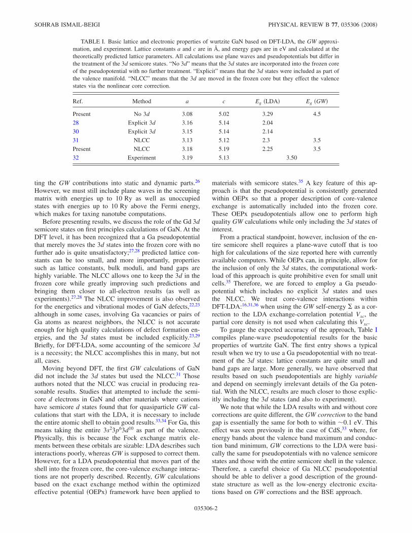
To gauge the expected accuracy of the approach, Table Icompiles plane-wave pseudopotential results for the basicproperties of wurtzite GaN. The first entry shows a typicalresult when we try to use a Ga pseudopotential with no treat-ment of the 3d states: lattice constants are quite small andband gaps are large. More generally, we have observed thatresults based on such pseudopotentials are highly variableand depend on seemingly irrelevant details of the Ga poten-tial. With the NLCC, results are much closer to those explic-itly including the 3d states �and also to experiment�.
We note that while the LDA results with and without corecorrections are quite different, the GW correction to the bandgap is essentially the same for both to within �0.1 eV. Thiseffect was seen previously in the case of CdS,33 where, forenergy bands about the valence band maximum and conduc-tion band minimum, GW corrections to the LDA were basi-cally the same for pseudopotentials with no valence semicorestates and those with the entire semicore shell in the valence.Therefore, a careful choice of Ga NLCC pseudopotentialshould be able to deliver a good description of the ground-state structure as well as the low-energy electronic excita-tions based on GW corrections and the BSE approach.
TABLE I. Basic lattice and electronic properties of wurtzite GaN based on DFT-LDA, the GW approxi-mation, and experiment. Lattice constants a and c are in Å, and energy gaps are in eV and calculated at thetheoretically predicted lattice parameters. All calculations use plane waves and pseudopotentials but differ inthe treatment of the 3d semicore states. “No 3d” means that the 3d states are incorporated into the frozen coreof the pseudopotential with no further treatment. “Explicit” means that the 3d states were included as part ofthe valence manifold. “NLCC” means that the 3d are moved in the frozen core but they effect the valencestates via the nonlinear core correction.
Ref. Method a c Eg �LDA� Eg �GW�
Present No 3d 3.08 5.02 3.29 4.5
28 Explicit 3d 3.16 5.14 2.04
30 Explicit 3d 3.15 5.14 2.14
31 NLCC 3.13 5.12 2.3 3.5
Present NLCC 3.18 5.19 2.25 3.5
32 Experiment 3.19 5.13 3.50
SOHRAB ISMAIL-BEIGI PHYSICAL REVIEW B 77, 035306 �2008�
035306-2
II. SHEETLIKE (TWO-DIMENSIONAL) FORM OF GaN
To properly orient a study of GaNNTs, we begin with thephysics of the two-dimensional sheetlike material fromwhich the nanotubes are constructed. We perform LDA cal-culations on a variety of possible GaN sheet structures. Forexample, we consider graphiticlike hexagonal lattices, trian-gular and square lattices, bilayers of such sheets, flat andbuckled sheets, etc. The hexagonal sheet, isostructural to BNsheets,6 with lattice vector of 3.17 Å has the lowest energy.This sheet is metastable by 0.39 eV/atom when compared towurtzite GaN. Thus, fabrication of GaNNTs may require ki-netic growth techniques, but it is encouraging that AlN nano-tubular materials can be fabricated37 even though their sheetenergy is even higher at 0.68 eV/atom above bulk.38 For usebelow, we find optical phonon frequencies at � for the sheetat 288 cm−1 �out of plane� and 758 cm−1 �in plane�. Thequadratic elastic energy increase �E=��2 for in-planestretching by a fraction � has modulus �=20.6 eV/atom.
At the LDA level, this sheet has an indirect band gap of2.4 eV between the valence band maximum �VBM� at K andthe conduction band minimum �CBM� at �, and the smallestdirect gap is 3.1 eV at � and is optically allowed. When weinclude GW self-energy effects, the gap remains indirect �K→�� but increases to 5.0 eV. The minimum GW direct gapis 5.6 eV and at �. The VBM at M has an energy of 0.4 eVbelow the VBM at K. The GW corrections are much largerthan those of bulk GaN �see Table I�. Thus, bulk GW correc-tions cannot simply be copied over to reduced dimensionalsystems without serious loss of accuracy.11 A main physicalreason is the dissimilar screening. In a three-dimensional me-dium, all electric field lines emanating from an electron orhole are screened since there is material in all directions. Inreduced dimensions, field lines can easily leave the material,so screening is anisotropic and much reduced. It is thescreening behavior of the many-body medium that deter-mines the GW corrections to DFT.
Figure 1 shows the sheet band structure. The ionicity dif-ference of Ga and N causes the � and �* bands derived fromthe out-of-plane pz orbitals to split by a large energy. Ingraphene, these bands are degenerate at the Fermi energy atK.39 Here, a “memory” of this degeneracy remains: the �-�*
gap is smallest at K and the sheet VBM remains there.Figure 2 displays the imaginary part of the dielectric func-
tion for the sheet, which is directly related to the opticalabsorption cross section. The large and qualitative differ-ences between the single-particle RPA-GW and two-particleGW-BSE methods highlight the crucial role and increasedstrength of electron-hole attractions in reduced dimensionalsystems. The lowest-energy GW-BSE peak is from an exci-ton with binding energy of 1.3 eV. This is the sheet’s lowestexcitation and is composed of electrons and holes about �.
The fact that the sheet has an indirect gap has importantconsequences for the electronic excitations of the nanotubes.Within the zone-folding scheme for nanotubes,39 we fold thesheet bands along the chiral direction to find the nanotubestates. When considering direct interband transitions, “roll-ing” the sheet turns states about the sheet K point into nano-tube VBM states at the nanotube � for �n ,0� nanotubes,whereas the region about the sheet M point turns into thenanotube VBM at the nanotube � for �n ,n� tubes. The CBMis at � for both sheets and tubes. Thus, the nanotube’slowest-energy direct transitions will be at its � point and willtake place between states with differing sheet crystal mo-menta or equivalently different angular momenta about thetube axis. Optical transitions between them are forbidden bythis momentum mismatch, so we expect dipole-forbidden�dark� low-energy excitations in GaNNTs.
To state this in more general terms, when a sheetlike ma-terial with an indirect band gap is “rolled up” to create nano-tubes, the zone-folding scheme predicts that the lowest-energy nanotube interband transitions will be dark due to amismatch of crystal momenta. Ceteris paribus, we wouldexpect that the lowest-energy excitons would also be dark.
III. GaN NANOTUBES
A. Structure and vibrational properties
We now describe our results for GaN nanotubes. We be-gin with basic structural and vibrational properties. Table II
FIG. 1. �Color online� Quasiparticle bands for the hexagonalGaN sheet based on the GW approximation. The valence bandmaximum at K is the zero of energy. The bands outlined with redcircles are the � and �* bands arising from out-of-plane pz orbitals.The other bands are in-plane � and �* states.
FIG. 2. �Color online� Imaginary part of the frequency-dependent dielectric function 2�� for the hexagonal GaN sheetbased on the RPA approximation with GW band energies �redcircles� and based on the BSE which includes excitonic effects�solid blue�. The first BSE peak corresponds to the bright exciton at4.3 eV.
ELECTRONIC EXCITATIONS IN SINGLE-WALLED GaN… PHYSICAL REVIEW B 77, 035306 �2008�
035306-3
describes the nanotubes that we have considered. For eachnanotube indexed by �n ,m�, we perform calculations byplacing the nanotube axis along the z direction. This is thephysically periodic direction with primitive lattice constantaz in the table. The choice of �n ,m� determines Nat, which isthe number of atoms per unit cell along z. We choose thesupercell to be square in the xy plane. Since we use theCoulomb truncation method,24 the actual shape or precisedimension of the cell in the xy direction is not relevant onceit is large enough to ensure convergence of calculated quan-tities. The length of the side of the square in the xy planewhere convergence is achieved is axy in the table and is thevalue we employ.
We relax the nanotube structures within LDA. Our start-ing guess for the structure is generated by rolling the GaNsheet into the nanotube. As found previously,11 the N atomslie at a larger radius than the Ga atoms from the nanotubecentral axis. Therefore, the diameter d in the table is theaverage of the two values. The difference in radius, the radialbuckling �r, decays to zero with increasing diameter. Wealso report the direct LDA band gap at the nanotube � pointin the table. The �n ,0� and �n ,n� direct band gaps behavedifferently and approach different values: for very largetubes, these turn into to the K→� and M→� transitions of
the sheet with LDA band gaps of 2.4 and 2.8 eV, respec-tively.
Previous work has reported on ground-state propertiessuch as structure, strain energies, or mechanicalproperties,11,13–15 so we concentrate on other findings. SinceRaman spectroscopy is an important tool for experimentalidentification of nanotubes,7,40 we describe the basic data forimportant long-wavelength phonons corresponding to radialbreathing modes. We calculate phonon frequencies of a fewGaNNTs within LDA, and Table III lists the results. Thesymmetric mode where Ga and N move radially and in phasehas frequency �s, while the out-of-phase mode has frequency�a. For a large nanotubes where d→ , these modes revert tothose of the sheet: the symmetric mode turns into an arbi-trarily long wavelength in-plane stretch, and the antisymmet-ric mode turns into the out-of-plane optical mode at � of thesheet, i.e., �s→0 and �a→288 cm−1.
In Fig. 3, we show the frequencies of both modes versusd. We note that lack of dependence of the frequencies on theclass of nanotube, which mirrors the behavior of the strain
TABLE II. The set of GaN nanotubes in this work for which LDA calculations are performed. All lengthsare in Å. Listed are the nanotube �n ,m� indices, the number of atoms per unit cell along the nanotube lengthNat, the size of the square base of the unit cell in the x and y directions axy, the length of the unit cell alongthe nanotube or z direction az, the mean diameter d, the radial buckling �r, and the direct LDA band gap forthe nanotube Eg
LDA �in eV�. See text for details.
Tube Nat axy az d �r EgLDA
�4,0� 16 12 5.15 4.41 0.25 1.93
�5,0� 20 13 5.25 5.34 0.21 1.90
�6,0� 24 13 5.43 6.24 0.17 1.88
�7,0� 28 14 5.45 7.20 0.14 2.02
�3,3� 12 13 3.12 5.40 0.21 2.09
�4,4� 16 15 3.11 7.14 0.16 2.31
�5,5� 20 17 3.18 8.78 0.12 2.31
�6,6� 24 19 3.18 10.5 0.10 2.42
TABLE III. Vibrational frequencies in cm−1 for radial breathingmodes of GaN nanotubes based on LDA calculations. d is the meannanotube diameter in Å. The frequency �s is for the symmetricmode where Ga and N move in phase, and �a is for the antisym-metric out-of-phase mode.
Tube d �s �a
�4,0� 4.41 193 439
�5,0� 5.34 168 406
�6,0� 6.24 151 370
�7,0� 7.20 135 353
�3,3� 5.40 166 399
�4,4� 7.14 137 358
�5,5� 8.78 116 335
FIG. 3. �Color online� Radial breathing mode frequencies incm−1 versus nanotube diameter d in Å. The upper set of data is forthe antisymmetric mode �a, and the lower set of data is for thesymmetric mode �s. Open �blue� triangles are for �n ,0� nanotubes,while �green� circles are for �n ,n� nanotubes. The upper continuousdashed curve is �a=288+2070 /d2, and the lower solid continuouscurve is �s=1040 /d.
SOHRAB ISMAIL-BEIGI PHYSICAL REVIEW B 77, 035306 �2008�
035306-4
energies:11 the results for �n ,0� and �n ,n� lie on the samecurve versus diameter. We have only calculated results forthe achiral �n ,0� and �n ,n� tubes. However, since these twoare the extreme cases for the choice of chiral angle,39 weexpect that results for other chiral nanotubes should lie be-tween the two extremes. Under this assumption, we expectno chirality dependence to these vibrational frequencies inGaNNTs.
For the symmetric mode, one can make a simple analyti-cal model to extract �s versus d using the data from the GaNsheet alone. In a continuum elastic picture, the symmetricradial mode corresponds to in-plane stretching of a GaNsheet. As noted above, such stretches cost a potential energy�E=��2, when stretching by a fraction �. A radial displace-ment �r means �=�r /r. The kinetic energy per atom ism�r2 /2, where m is the average atomic mass of Ga and N.The frequency of this quadratic system is �s=�� / m / ��d�=1040 /d, with d in Å and �s in cm−1. We plot this curve inFig. 3: there is some deviation at small d, but for d�9 Å, theit is already less than 2% and will only improve for larger d.
The behavior of the antisymmetric mode �a is more diffi-cult to model analytically. To understand the scaling of �aversus d, we implement a recent tight-binding model forGaN.41 Although the model was designed for bulk systems,we have verified that it describes well the geometries of GaNsheets and nanotubes. We use this model to calculate phononfrequencies for a large sample of nanotubes. For the symmet-ric mode, we verify again that the behavior for large d is�s�d−1. For the antisymmetric mode, the behavior is �a=A+Bd−2 for constants A and B. We fit our ab initio data to thismathematical form: A must equal 288 cm−1 as explainedabove, and the best fit for B yields the final form �a=288+2070 /d2. By d�9 Å, the error is less than 4%. We empha-size that we have used the tight-binding model only to findthe mathematical form of the function but not any of theactual constants.
Finally, we note that there exists a tangential mode whereGa and N atoms move out of phase along the surface of thenanotube. When d→ , this mode turns into the in-planeoptical phonon of the sheet at � with frequency �t=758 cm−1. The tight-binding model predicts the behavior�t=C+Dd−2, where D�0. We have not calculated any abinitio data for this mode, so precise determination of D is not
possible. However, based on a crude scaling of the tight-binding data that sets C=758 cm−1, we roughly estimate that�t�758−2190 /d2.
B. Electronic and optical properties
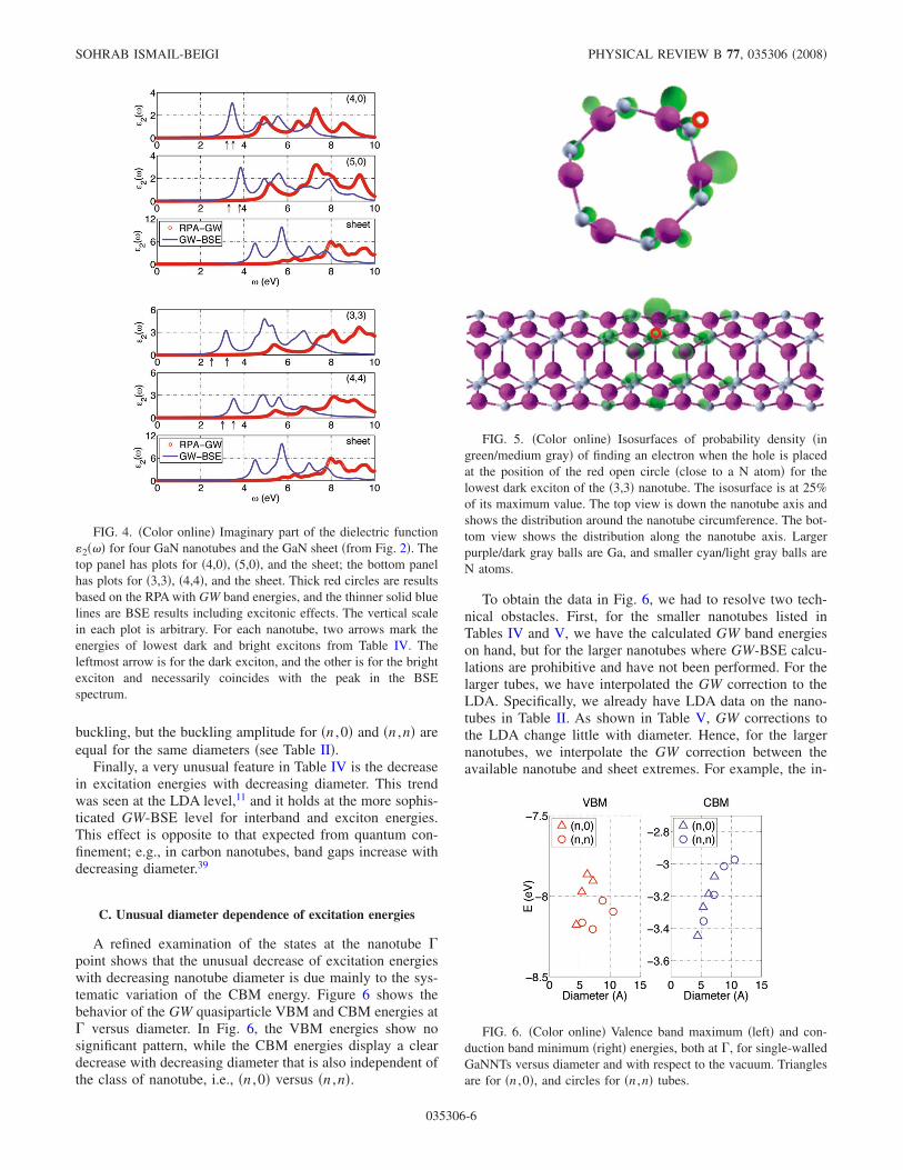
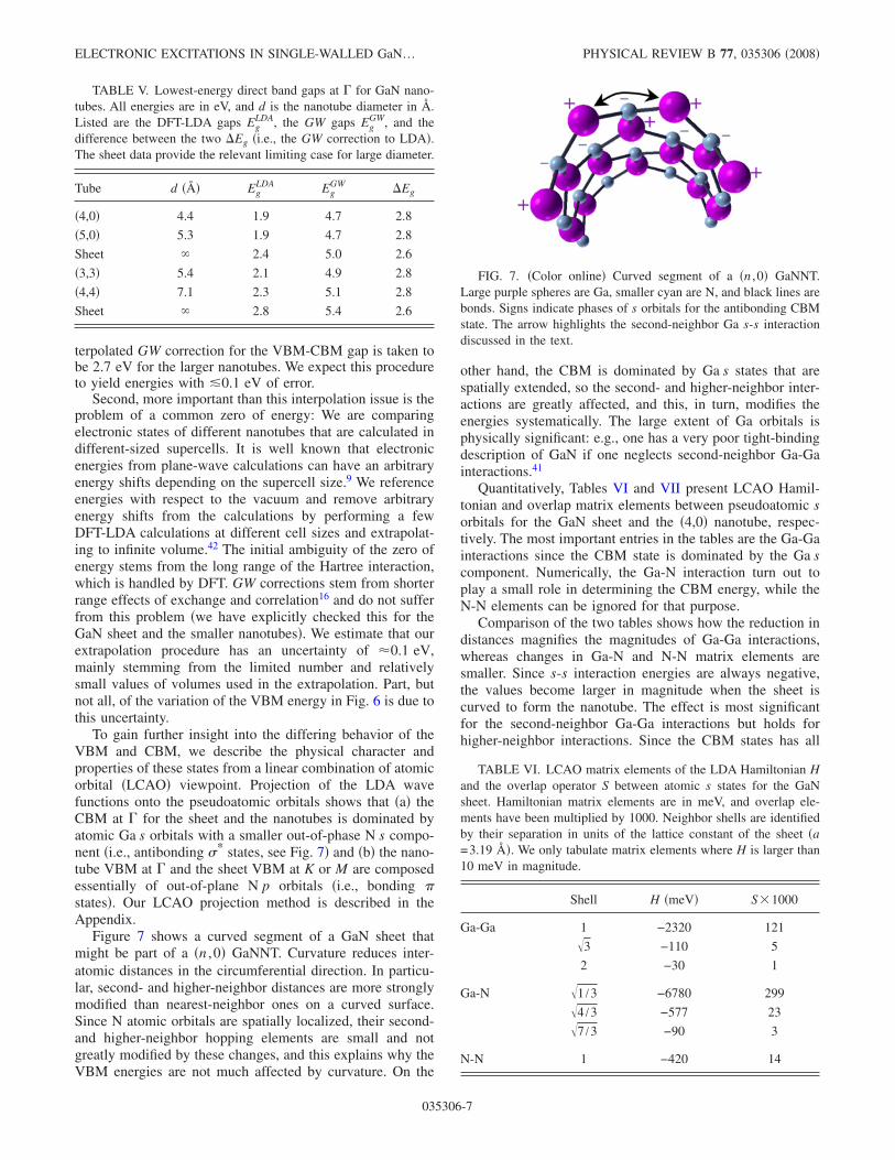
We now consider the electronic states of GaN nanotubes.Table IV summarizes our findings for the low-energy opticalproperties of four small-diameter achiral �n ,0� and �n ,n�nanotubes. Figure 4 shows the imaginary part of the dielec-tric function for each of these nanotubes. We now discusssalient features of these results. First, exciton binding ener-gies are large and �1–2 eV. Due to further dimensionalreduction, binding energies are larger in the nanotubes thanfor the sheet. �The exciton binding energy is the differencebetween the excitation energy � and the lowest interbandtransition Einter for which the exciton wave function has asizable amplitude.� Figure 5 shows a representative probabil-ity distribution for the lowest exciton of the �3,3� nanotube.Due to its large binding energy, the exciton is rather localizedboth around and along the nanotube axis. Second, as antici-pated, the lowest-energy excitons are dipole forbidden�dark�. There is a significant �0.5–1.0 eV difference be-tween the lowest dark and first bright exciton energies. Third,the bright excitons in �n ,0� and �n ,n� tubes both approachthe same limit: the sheet’s bright exciton. However, the darkexcitons approach different limits because, as per band fold-ing, the lowest direct transition for �n ,0� tubes correspondsto K→� in the sheet, whereas for �n ,n�, we have M→�.Based on the �n ,0� data, we estimate that the dark K→�excitons in large GaNNTs are at �3.6 eV with binding en-ergy of �1.4 eV.
Next, excitons in �n ,0� and �n ,n� tubes approach thesheet limit at different rates. Given a diameter, the �n ,0� aremuch closer to the sheet limit. The difference is large; forexample, for exciton binding energies, at d�5 Å, the �5,0�energy is within 0.1 eV of the sheet values, while the �3,3� is0.9 eV off. The difference is also visible in the plots of Fig.4; comparing the GW-BSE spectra for �5,0� and �3,3� to thesheet’s, we see that the �5,0� results are closer to the sheet forthe first and second low-energy peaks. We have not found thereason for the difference. For example, a key structural dif-ference between the sheet and the nanotubes is the radial
TABLE IV. Lowest-energy exciton energies in eV for single-walled GaNNTs. The lowest excitations aredark �dipole forbidden�; the lowest bright �optically allowed� exciton is also listed. d is the nanotube diam-eter, � the exciton energy, Einter the dominant interband transition for that exciton, and � the exciton bindingenergy. The sheet data provide the relevant limiting case for large diameter �Ref. 45�.
Tube d ��
Dark excitons Bright excitons
� Einter � � Einter �
�4,0� 4.4 3.2 4.7 1.5 3.5 4.9 1.5
�5,0� 5.4 3.3 4.7 1.4 3.8 5.2 1.4
Sheet 5.0 4.3 5.6 1.3
�3,3� 5.4 2.5 4.9 2.4 3.2 5.4 2.2
�4,4� 7.1 3.0 5.1 2.1 3.5 5.4 1.9
Sheet 5.4 4.3 5.6 1.3
ELECTRONIC EXCITATIONS IN SINGLE-WALLED GaN… PHYSICAL REVIEW B 77, 035306 �2008�
035306-5
buckling, but the buckling amplitude for �n ,0� and �n ,n� areequal for the same diameters �see Table II�.
Finally, a very unusual feature in Table IV is the decreasein excitation energies with decreasing diameter. This trendwas seen at the LDA level,11 and it holds at the more sophis-ticated GW-BSE level for interband and exciton energies.This effect is opposite to that expected from quantum con-finement; e.g., in carbon nanotubes, band gaps increase withdecreasing diameter.39
C. Unusual diameter dependence of excitation energies
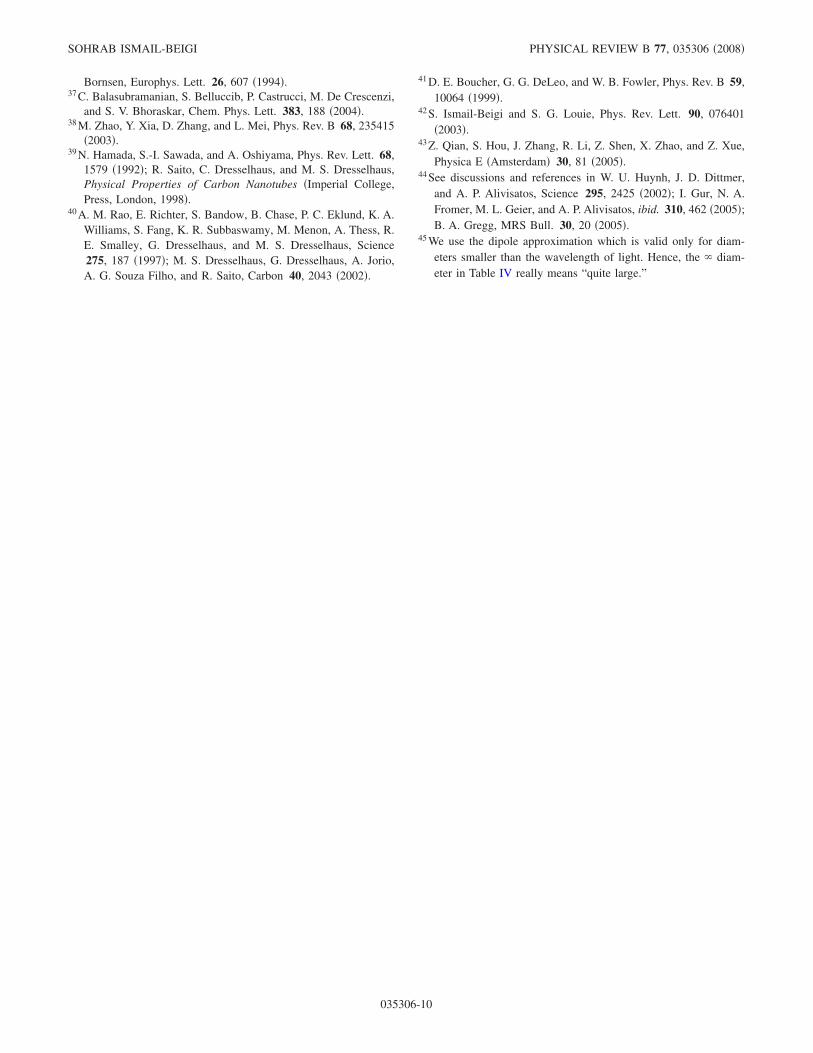
A refined examination of the states at the nanotube �point shows that the unusual decrease of excitation energieswith decreasing nanotube diameter is due mainly to the sys-tematic variation of the CBM energy. Figure 6 shows thebehavior of the GW quasiparticle VBM and CBM energies at� versus diameter. In Fig. 6, the VBM energies show nosignificant pattern, while the CBM energies display a cleardecrease with decreasing diameter that is also independent ofthe class of nanotube, i.e., �n ,0� versus �n ,n�.
To obtain the data in Fig. 6, we had to resolve two tech-nical obstacles. First, for the smaller nanotubes listed inTables IV and V, we have the calculated GW band energieson hand, but for the larger nanotubes where GW-BSE calcu-lations are prohibitive and have not been performed. For thelarger tubes, we have interpolated the GW correction to theLDA. Specifically, we already have LDA data on the nano-tubes in Table II. As shown in Table V, GW corrections tothe LDA change little with diameter. Hence, for the largernanotubes, we interpolate the GW correction between theavailable nanotube and sheet extremes. For example, the in-
FIG. 4. �Color online� Imaginary part of the dielectric function2�� for four GaN nanotubes and the GaN sheet �from Fig. 2�. Thetop panel has plots for �4,0�, �5,0�, and the sheet; the bottom panelhas plots for �3,3�, �4,4�, and the sheet. Thick red circles are resultsbased on the RPA with GW band energies, and the thinner solid bluelines are BSE results including excitonic effects. The vertical scalein each plot is arbitrary. For each nanotube, two arrows mark theenergies of lowest dark and bright excitons from Table IV. Theleftmost arrow is for the dark exciton, and the other is for the brightexciton and necessarily coincides with the peak in the BSEspectrum.
FIG. 5. �Color online� Isosurfaces of probability density �ingreen/medium gray� of finding an electron when the hole is placedat the position of the red open circle �close to a N atom� for thelowest dark exciton of the �3,3� nanotube. The isosurface is at 25%of its maximum value. The top view is down the nanotube axis andshows the distribution around the nanotube circumference. The bot-tom view shows the distribution along the nanotube axis. Largerpurple/dark gray balls are Ga, and smaller cyan/light gray balls areN atoms.
FIG. 6. �Color online� Valence band maximum �left� and con-duction band minimum �right� energies, both at �, for single-walledGaNNTs versus diameter and with respect to the vacuum. Trianglesare for �n ,0�, and circles for �n ,n� tubes.
SOHRAB ISMAIL-BEIGI PHYSICAL REVIEW B 77, 035306 �2008�
035306-6
terpolated GW correction for the VBM-CBM gap is taken tobe 2.7 eV for the larger nanotubes. We expect this procedureto yield energies with �0.1 eV of error.
Second, more important than this interpolation issue is theproblem of a common zero of energy: We are comparingelectronic states of different nanotubes that are calculated indifferent-sized supercells. It is well known that electronicenergies from plane-wave calculations can have an arbitraryenergy shifts depending on the supercell size.9 We referenceenergies with respect to the vacuum and remove arbitraryenergy shifts from the calculations by performing a fewDFT-LDA calculations at different cell sizes and extrapolat-ing to infinite volume.42 The initial ambiguity of the zero ofenergy stems from the long range of the Hartree interaction,which is handled by DFT. GW corrections stem from shorterrange effects of exchange and correlation16 and do not sufferfrom this problem �we have explicitly checked this for theGaN sheet and the smaller nanotubes�. We estimate that ourextrapolation procedure has an uncertainty of �0.1 eV,mainly stemming from the limited number and relativelysmall values of volumes used in the extrapolation. Part, butnot all, of the variation of the VBM energy in Fig. 6 is due tothis uncertainty.
To gain further insight into the differing behavior of theVBM and CBM, we describe the physical character andproperties of these states from a linear combination of atomicorbital �LCAO� viewpoint. Projection of the LDA wavefunctions onto the pseudoatomic orbitals shows that �a� theCBM at � for the sheet and the nanotubes is dominated byatomic Ga s orbitals with a smaller out-of-phase N s compo-nent �i.e., antibonding �* states, see Fig. 7� and �b� the nano-tube VBM at � and the sheet VBM at K or M are composedessentially of out-of-plane N p orbitals �i.e., bonding �states�. Our LCAO projection method is described in theAppendix.
Figure 7 shows a curved segment of a GaN sheet thatmight be part of a �n ,0� GaNNT. Curvature reduces inter-atomic distances in the circumferential direction. In particu-lar, second- and higher-neighbor distances are more stronglymodified than nearest-neighbor ones on a curved surface.Since N atomic orbitals are spatially localized, their second-and higher-neighbor hopping elements are small and notgreatly modified by these changes, and this explains why theVBM energies are not much affected by curvature. On the
other hand, the CBM is dominated by Ga s states that arespatially extended, so the second- and higher-neighbor inter-actions are greatly affected, and this, in turn, modifies theenergies systematically. The large extent of Ga orbitals isphysically significant: e.g., one has a very poor tight-bindingdescription of GaN if one neglects second-neighbor Ga-Gainteractions.41
Quantitatively, Tables VI and VII present LCAO Hamil-tonian and overlap matrix elements between pseudoatomic sorbitals for the GaN sheet and the �4,0� nanotube, respec-tively. The most important entries in the tables are the Ga-Gainteractions since the CBM state is dominated by the Ga scomponent. Numerically, the Ga-N interaction turn out toplay a small role in determining the CBM energy, while theN-N elements can be ignored for that purpose.
Comparison of the two tables shows how the reduction indistances magnifies the magnitudes of Ga-Ga interactions,whereas changes in Ga-N and N-N matrix elements aresmaller. Since s-s interaction energies are always negative,the values become larger in magnitude when the sheet iscurved to form the nanotube. The effect is most significantfor the second-neighbor Ga-Ga interactions but holds forhigher-neighbor interactions. Since the CBM states has all
TABLE V. Lowest-energy direct band gaps at � for GaN nano-tubes. All energies are in eV, and d is the nanotube diameter in Å.Listed are the DFT-LDA gaps Eg
LDA, the GW gaps EgGW, and the
difference between the two �Eg �i.e., the GW correction to LDA�.The sheet data provide the relevant limiting case for large diameter.
Tube d �� EgLDA Eg
GW �Eg
�4,0� 4.4 1.9 4.7 2.8
�5,0� 5.3 1.9 4.7 2.8
Sheet 2.4 5.0 2.6
�3,3� 5.4 2.1 4.9 2.8
�4,4� 7.1 2.3 5.1 2.8
Sheet 2.8 5.4 2.6
TABLE VI. LCAO matrix elements of the LDA Hamiltonian Hand the overlap operator S between atomic s states for the GaNsheet. Hamiltonian matrix elements are in meV, and overlap ele-ments have been multiplied by 1000. Neighbor shells are identifiedby their separation in units of the lattice constant of the sheet �a=3.19 �. We only tabulate matrix elements where H is larger than10 meV in magnitude.
Shell H �meV� S�1000
Ga-Ga 1 −2320 121�3 −110 5
2 −30 1
Ga-N �1 /3 −6780 299�4 /3 −577 23�7 /3 −90 3
N-N 1 −420 14
FIG. 7. �Color online� Curved segment of a �n ,0� GaNNT.Large purple spheres are Ga, smaller cyan are N, and black lines arebonds. Signs indicate phases of s orbitals for the antibonding CBMstate. The arrow highlights the second-neighbor Ga s-s interactiondiscussed in the text.
ELECTRONIC EXCITATIONS IN SINGLE-WALLED GaN… PHYSICAL REVIEW B 77, 035306 �2008�
035306-7
Ga s states in phase �see Fig. 7�, the enhanced Ga s-s matrixelements between all the Ga atoms add together and lowerthe CBM energy. Obviously, this result cannot be explainedby a simple appeal to a nearest-neighbor bonding picture:reduced distances would lead us to expect larger bonding-antibonding splittings and the opposite trend versus diameter.
In summary, the unusual behavior versus diameter is dueto the chemistry of Ga combined with curvature effects ac-cessible only at the nanoscale. The effect follows from thetwo rather generic facts that Ga atomic orbitals are spatiallyextended and that the CBM state is dominated by Ga atomicorbitals. Thus, this behavior and explanation should not bespecific to the LDA or other approximations employed here.Moreover, this mechanism can apply in other materials con-taining cations with large atomic orbitals and provides an-other way to reduce band gaps and excitation energies withdecreasing size.
CONCLUSIONS
We have offered state-of-the-art ab initio theoretical pre-dictions of the basic vibrational, electronic, optical, and ex-citonic properties of gallium nitride nanotubes as well as thetwo-dimensional sheet form of GaN which gives rise to thenanotubes. We have shown that electron-hole interactionslead to strongly bound excitons and dramatically modify theoptical spectra when compared to simple interband predic-tions.
The GaN sheet is shown to be an indirect band-gap ma-terial which makes for nanotubes whose lowest-energy direct
transitions are optically forbidden �dark�. This carries over tothe excitons; the lowest-energy excitons in the nanotubes arealso found to be dark. Finally, we have observed and ex-plained an unusual decrease in excitation energies with de-creasing diameter that opposes expectations based on theusual picture of quantum confinement in nanostructures. Thisunconventional behavior is due to a combination of nano-scopic curvature and the chemistry of gallium, can apply toother materials, and provides another method to reduce ex-citation energies with decreasing size.
We end with some implications and speculations. As lu-minescent materials, GaNNTs may fare poorly due to theunavoidable low-energy dark excitons; once excitons arethermalized in the nanotubes, the excitons have relativelyweak radiative strength. This conclusion should also apply toInN nanotubes because their sheet forms have indirect bandgaps as well.43
Conversely, this very property makes these materials use-ful when long-lived excitons are needed. For example, incurrent candidates for low-cost photovoltaic materials, pho-togenerated excitons must first diffuse through the materialin which they are created to reach an interface with anothermaterial. There, the exciton can dissociate across the inter-face into free carriers which then travel in opposite directionsto create a current.44 Clearly, this entire process is more ef-fective and efficient if the radiative lifetime of the excitons isnot a bottleneck during the �relatively slow� diffusion to theinterface.
Our results show that the optical absorption of GaNNTsbegins at �3.5–4.0 eV, which is beyond the visible spec-trum but can be useful for UV applications. To reduce thisenergy into the visible, InN or alloyed Ga / InN nanotubesmay be considered. As explained above, the unusual band-gap behavior versus diameter should apply also to InN nano-tubes because it stems from the large size of the cationatomic orbitals, a property shared by In and Ga. This class ofmaterials likely offers strong and tunable absorption com-bined with very long exciton lifetimes.
ACKNOWLEDGMENTS
We thank Lisa Pfefferle and Jung Han for sharing theirinterest and knowledge which inspired this work. This workwas supported primarily by the National Science Foundationunder Contract No. MRSEC DMR 0520495. The Bulldogparallel clusters of the Yale High Performance Computingcenter provided computing resources.
APPENDIX
Here, we describe the simple LCAO projection methodemployed in the analysis, discussion, and tables of Sec. III C.During the generation of pseudopotentials for Ga and N, weobtain the atomic radial functions Rinl�r�, where i labels theatom and n, l are standard atomic quantum numbers. Theatomic pseudo-wave-function is
where r�i is the position of atom i and the Ylm are sphericalharmonics centered at position r�i. We wish to find LCAO
TABLE VII. LCAO matrix elements of the LDA Hamiltonian Hand the overlap operator S between atomic s states for the �4,0�nanotube. Hamiltonian matrix elements are in meV, and overlapelements have been multiplied by 1000. rij /a is the interatomicdistance in units of the sheet lattice constant a. The column “Sheetshell” identifies the sheet neighbor shell to which the interactionbelongs in the nomenclature of Table VI. We only tabulate matrixelements where H is larger than 100 meV in magnitude.
rij /a Sheet shell H �meV� S�1000
Ga-Ga 0.942 1 −2920 150
0.967 1 −2670 140
1.33 2 −591 31
1.48 �3 −337 16
1.64 �3 −180 7
Ga-N 0.584 �1 /3 −6760 293
0.596 �1 /3 −6490 280
1.07 �4 /3 −878 34
1.15 �4 /3 −614 22
1.33 �7 /3 −261 9
1.46 �7 /3 −133 4
1.50 �7 /3 −103 4
N-N 1.00 1 −444 13
1.05 1 −328 9
SOHRAB ISMAIL-BEIGI PHYSICAL REVIEW B 77, 035306 �2008�
035306-8
matrix elements of the Hamiltonian �H� and overlap �S� be-tween two atomic orbitals,
Hinlm , i�n�l�m� = ��inlm�H��i�n�l�m�� ,
Sinlm , i�n�l�m� = ��inlm��i�n�l�m�� .
Above, H is the DFT Hamiltonian operator.In principle, a variety of approaches can be used to com-
pute H and S. We opt for the simplest one. Performing theGW calculations requires a large number of single-particle
orthonormal Bloch eigenstates � jk� of H along with their en-ergies Ejk�, where j is the band index and k� is the crystalmomentum. We employ completeness to write H and S as
Hinlm , i�n�l�m� = j,k�
��inlm�� jk��Ejk��� jk���i�n�l�m�� ,
Sinlm , i�n�l�m� = j,k�
��inlm�� jk���� jk���i�n�l�m�� .
The precision is limited by the cutoff in the sum over j.Convergence is monitored easily: the diagonals of H and Sapproach convergence from below, the diagonals of S ap-proach unity, and off-diagonal elements of S between differ-ent orbitals on the same atom approach zero. Computinginner products such as ��inlm �� j,k�� is standard for DFT cal-culations with nonlocal pseudopotentials;9 one uses theplane-wave expansion of � j,k� together with the standard text-book expansion of a plane wave into spherical waves aboutan arbitrary point �r�i or r�i��.
1 S. Nakamura, T. Mukai, and M. Senoh, Appl. Phys. Lett. 64,1687 �1994�; F. A. Ponce and D. P. Bour, Nature �London� 386,351 �1997�.
2 M. Asif Khan, Q. Chen, Michael S. Shur, B. T. Dermott, J. A.Higgins, J. Burm, W. J. Schaff, and L. F. Eastman, Solid-StateElectron. 41, 1555 �1997�.
3 W. Han, S. Fan, Q. Li, and Y. Hu, Science 277, 1287 �1997�; X.F. Duan and C. M. Lieber, J. Am. Chem. Soc. 122, 188 �2000�;J. C. Johnson, H.-J. Choi, K. P. Knutsen, R. D. Schaller, P. Yang,and R. Saykally, Nat. Mater. 1, 106 �2002�; V. Dobrokhotov, D.N. Mcllroy, M. G. Norton, A. Abuzir, W. J. Yeh, I. Stevenson, R.Pouy, J. Bochenek, M. Cartwright, L. Wang, J. Dawson, M.Beaux, and C. Berven, J. Appl. Phys. 99, 104302 �2006�.
4 Z. Liliental-Weber, Y. Chen, S. Ruvimov, and J. Washburn, Phys.Rev. Lett. 79, 2835 �1997�; J. Goldberger, R. He, Y. Zhang, S.Lee, H. Yan, H.-J. Choi, and P. Yang, Nature �London� 422, 599�2003�.
5 S. Iijima, Nature �London� 354, 56 �1991�.6 N. G. Chopra, R. J. Luyken, K. Cherrey, V. H. Crespi, M. L
Cohen, S. G. Louie, and A. Zettl, Science 269, 966 �1995�; A.Rubio, J. L. Corkill, and M. L. Cohen, Phys. Rev. B 49, R5081�1994�.
7 D. Ciuparu, R. F. Klie, Y. Zhu, and L. Pfefferle, J. Phys. Chem. B108, 3967 �2004�.
8 P. Hohenberg and W. Kohn, Phys. Rev. 136, B864 �1964�; W.Kohn and L. Sham, Phys. Rev. 140, A1133 �1965�.
9 M. C. Payne, M. P. Teter, D. C. Allan, T. A. Arias, and J. D.Joannopoulos, Rev. Mod. Phys. 64, 1045 �1992�.
10 L. Kleinman and D. M. Bylander, Phys. Rev. Lett. 48, 1425�1982�.
11 S. M. Lee, Y. H. Lee, Y. G. Hwang, J. Elsner, D. Porezag, and T.Frauenheim, Phys. Rev. B 60, 7788 �1999�.
12 S. Hao, G. Zhou, J. Wu, W. Duan, and B.-L. Gu, Phys. Rev. B 69,113403 �2004�.
13 E. Durgun, S. Tongay, and S. Ciraci, Phys. Rev. B 72, 075420�2005�.
14 M. Zhang, Z.-M. Su, L.-K. Yana, Y.-Q. Qiu, G.-H. Chen, andR.-S. Wang, Chem. Phys. Lett. 408, 145 �2005�.
15 B. Xu and B. C. Pan, Phys. Rev. B 74, 245402 �2006�.
16 M. S. Hybertsen and S. G. Louie, Phys. Rev. B 34, 5390 �1986�.17 Theory of the Inhomogeneous Electron Gas, edited by S. Lund-
qvist and N. H. March �Plenum, New York 1983�, and refer-ences therein.
18 S. Albrecht, L. Reining, R. Del Sole, and G. Onida, Phys. Rev.Lett. 80, 4510 �1998�; L. X. Benedict, E. L. Shirley, and R. B.Bohn, ibid. 80, 4514 �1998�; M. Rohlfing and S. G. Louie, ibid.81, 2312 �1998�.
19 M. Rohlfing and S. G. Louie, Phys. Rev. B 62, 4927 �2000�.20 G. Onida, L. Reining, and A. Rubio, Rev. Mod. Phys. 74, 601
�2002�.21 S. G. Louie, S. Froyen, and M. L. Cohen, Phys. Rev. B 26, 1738
�1982�.22 S. Limpijumnong, J. E. Northrup, and C. G. Van de Walle, Phys.
Rev. B 68, 075206 �2003�, and references therein.23 S. Limpijumnong and C. G. Van de Walle, Phys. Rev. B 69,
035207 �2004�, and references therein.24 S. Ismail-Beigi, Phys. Rev. B 73, 233103 �2006�.25 H. Ajiki and T. Ando, Physica B 201, 349 �1994�.26 F. Bechstedt, R. Del Sole, G. Cappellini, and L. Reining, Solid
State Commun. 84, 765 �1992�.27 V. Fiorentini, M. Methfessel, and M. Scheffler, Phys. Rev. B 47,
13353 �1993�.28 A. F. Wright and J. S. Nelson, Phys. Rev. B 50, 2159 �1994�.29 J. Neugebauer, T. Zywietz, M. Scheffler, J. E. Northrup, and C.
G. Van de Walle, Phys. Rev. Lett. 80, 3097 �1998�.30 A. Janotti, D. Segev, and C. G. Van de Walle, Phys. Rev. B 74,
045202 �2006�.31 A. Rubio, J. L. Corkill, M. L. Cohen, E. L. Shirley, and S. G.
Louie, Phys. Rev. B 48, 11810 �1993�.32 Semiconductors—Basic Data, 2nd revised ed., edited by O.
Madelung �Springer, Berlin, 1996�.33 M. Rohlfing, P. Kruger, and J. Pollmann, Phys. Rev. Lett. 75,
3489 �1995�.34 M. Rohlfing, P. Kruger, and J. Pollmann, Phys. Rev. B 57, 6485
�1998�.35 P. Rinke, A. Qtiesh, J. Neugebauer, C. Freysoldt, and M. Schef-
fler, New J. Phys. 7, 126 �2005�.36 M. Palummo, L. Reining, R. W. Godby, C. M. Bertonni, and N.
ELECTRONIC EXCITATIONS IN SINGLE-WALLED GaN… PHYSICAL REVIEW B 77, 035306 �2008�
035306-9
Bornsen, Europhys. Lett. 26, 607 �1994�.37 C. Balasubramanian, S. Belluccib, P. Castrucci, M. De Crescenzi,
and S. V. Bhoraskar, Chem. Phys. Lett. 383, 188 �2004�.38 M. Zhao, Y. Xia, D. Zhang, and L. Mei, Phys. Rev. B 68, 235415
�2003�.39 N. Hamada, S.-I. Sawada, and A. Oshiyama, Phys. Rev. Lett. 68,
1579 �1992�; R. Saito, C. Dresselhaus, and M. S. Dresselhaus,Physical Properties of Carbon Nanotubes �Imperial College,Press, London, 1998�.
40 A. M. Rao, E. Richter, S. Bandow, B. Chase, P. C. Eklund, K. A.Williams, S. Fang, K. R. Subbaswamy, M. Menon, A. Thess, R.E. Smalley, G. Dresselhaus, and M. S. Dresselhaus, Science275, 187 �1997�; M. S. Dresselhaus, G. Dresselhaus, A. Jorio,A. G. Souza Filho, and R. Saito, Carbon 40, 2043 �2002�.
41 D. E. Boucher, G. G. DeLeo, and W. B. Fowler, Phys. Rev. B 59,10064 �1999�.
42 S. Ismail-Beigi and S. G. Louie, Phys. Rev. Lett. 90, 076401�2003�.
43 Z. Qian, S. Hou, J. Zhang, R. Li, Z. Shen, X. Zhao, and Z. Xue,Physica E �Amsterdam� 30, 81 �2005�.
44 See discussions and references in W. U. Huynh, J. D. Dittmer,and A. P. Alivisatos, Science 295, 2425 �2002�; I. Gur, N. A.Fromer, M. L. Geier, and A. P. Alivisatos, ibid. 310, 462 �2005�;B. A. Gregg, MRS Bull. 30, 20 �2005�.
45 We use the dipole approximation which is valid only for diam-eters smaller than the wavelength of light. Hence, the diam-eter in Table IV really means “quite large.”
SOHRAB ISMAIL-BEIGI PHYSICAL REVIEW B 77, 035306 �2008�