CHAPTER 1 ELECTRONICS AND SEMICONDUCTORS Chapter Outline 1.1 Signals 1.2 Frequency Spectrum of Signals 1.3 Analog and Digital Signals 1.4 Amplifiers 1.5 Circuit Models for Amplifiers 1.6 Frequency Response of Amplifiers 1.7 Intrinsic Semiconductors 18 Doped Semiconductors NTUEE Electronics – L. H. Lu 1-1 1.8 Doped Semiconductors 1.9 Current Flow in Semiconductors 1.10 The pn Junction with Open-Circuit Terminals 1.11 The pn Junction with Applied Voltage 1.12 Capacitive Effects in the pn Junction
Transcript
CHAPTER 1 ELECTRONICS AND SEMICONDUCTORS
Chapter Outline1.1 Signals1.2 Frequency Spectrum of Signals1.3 Analog and Digital Signals1.4 Amplifiers1.5 Circuit Models for Amplifiers1.6 Frequency Response of Amplifiers1.7 Intrinsic Semiconductors1 8 Doped Semiconductors
NTUEE Electronics – L. H. Lu 1-1
1.8 Doped Semiconductors1.9 Current Flow in Semiconductors1.10 The pn Junction with Open-Circuit Terminals1.11 The pn Junction with Applied Voltage1.12 Capacitive Effects in the pn Junction
1.1 Signals
Signal processingSignals can be of a variety of forms in order to carry information from the physical world.It is most convenient to process signals by electronic system, therefore, the signals are first converted into
an electric form (voltage or current) by transducers.
SignalProcessorInput Signal
(voice, speed,pressure, etc.)
Output Signal(voice, speed,pressure, etc.)
Transducer Transducer
Electric Signals Electric Signals
t
v(t)
t
v(t)
Signal sourcesThevenin form: (voltage source vs + series resistance Rs) Presenting the signal by voltage form. Is preferred when Rs is low.
Norton form: (current source is + shunt resistance Rs) Presenting the signal by current form. Is preferred when Rs is high.
In electronics systems, the signal is taken from one of the two forms for analysis.Two forms are interchangeable with vs(t) = is(t) Rs.
NTUEE Electronics – L. H. Lu 1-2
1.2 Frequency Spectrum of Signals
Sinusoidal signalIn time domain, a sinusoidal signal is given as: va(t) = Vasin( t + )Can be characterized by its amplitude (Va), frequency () and phase ()Any time-domain signal can be expressed by its frequency spectrum. Periodic signal Fourier series Non-periodic signal Fourier transform
Periodic signalThe fundamental frequency of periodic signal is defined as 0 = 2/T.A periodic signal can be expressed as the sum of sinusoids at harmonic frequencies (n0) by Fourier series.
Non-periodic signalThe Fourier transform is applied to a non-periodic function of time.The spectrum of a non-periodic signal contains all possible frequencies.
Signal classificationAnalog signal: signal can take on any value.Digital signal: can only take on finite quantization levels.Continuous-time signal: defined at any time instant.Discrete-time signal: defined only at the sampling instants.Sampling: the amplitude is measured at equal time intervals.Quantization: represent the samples by a finite values.Quantization error: Difference between sampled value and quantized value. Can be reduced by increasing the quantization levels
Continuous-time analog signalv(t)
t
Discrete-time analog signal Sampling
Can be reduced by increasing the quantization levels.Data conversionAnalog-to-digital converter (ADC):
Digital-to-analog converter (DAC):
NTUEE Electronics – L. H. Lu 1-5
A/Dconverter ...
b0b1
bN-1
vA
Analoginput
Digitaloutput
D/Aconverter...
b0b1
bN-1
vD
Analogoutput
Digitalinput
vA = vD + quantization error
111
00 2....22 N
ND bbbv
3,3,3,2,3,3…
Digital signal
Quantization error
t
Quantization3
2
1
0t
t
1.4 Amplifiers
Gain of amplifiersVoltage gain Av vO / vI
Current gain Ai iO / iI
Power gain Ap vO iO / vI iI
Amplifier gains are dimensionless (ratio of similarly dimensioned quantities).Voltage and current gain can be positive or negative depending on the polarity of the voltage and current.The gain is frequently expressed in decibels: Voltage gain Av (dB) 20 log | Av | Current gain Ai (dB) 20 log | Ai | Power gain A (dB) 10 log | A | Power gain Ap (dB) 10 log | Ap | Gain > 0 dB | A | > 1 (amplification) Gain < 0 dB | A | < 1 (attenuation) The polarity of the voltage and current is not shown in dB expression.
Amplifier power suppliesAmplifiers require dc power supplies.Pdc = VCC ICC + VEE IEE
Pdc + PI = PL + Pdissipated
(efficiency) = (PL / Pdc )100%
NTUEE Electronics – L. H. Lu 1-6
Transfer characteristics of linear amplifierThe plot of output response vs. input transfer characteristicsFor linear amplifier, the transfer characteristics is a straight line
passing the origin with slope = Av.It is desirable to have linear amplifier characteristics for most of
the applications.Output waveform is an enlarged copy of the input: vO(t) = AvvI(t)No higher power terms of vI at the output.
Amplifier saturationAmplifier saturationPractically, the amplifier transfer characteristic remains linear
over only a limited range of input and output voltages.The amplifier can be used as a linear amplifier for input swing:
L/Av vI L+/Av vO = AvvI
For input larger than the swing limitation, the output waveformwill be truncated, resulting in nonlinear distortion.
The nonlinearity properties can be expressed as:vO = a0 + a1vI + a2vI
2 + a3vI3 …..
NTUEE Electronics – L. H. Lu 1-7
Nonlinear transfer characteristics and biasingIn practical amplifiers the transfer characteristic may exhibit nonlinearities of various magnitude.The nonlinearity characteristics will result in signal distortion during amplification.In order to use the circuit as a linear amplifier: Use dc bias to operate the circuit near the middle of the transfer curve quiescent point. Superimpose the time-varying (ac) signal on the dc bias at the input. Be sure that the signal swing is sufficiently small for good linear approximation. The time-varying (ac) components at the output is the desired output signal.
Concept of equivalent circuitPractical amplifier circuit could be rather complexUse a simplified model to represent the properties and behavior of the amplifierThe analysis results do not change by replacing the original circuit with the equivalent circuit
Voltage amplifiersA simplified two-port model is widely used for unilateral voltage amplifiers
Voltage Amplifier
The model is composed of three components: Input resistance (Ri): the resistance by looking into the input port Output resistance (Ro): the resistance by looking into the output port Open-circuit voltage gain (Avo): the voltage gain (vo/vi) with output open-circuit
Circuit analysis with signal source and load:
Voltage gain:
Overall gain:
Ideal voltage amplifier: Ri = and Ro = 0
NTUEE Electronics – L. H. Lu 1-10
oL
Lvo
i
ov RR
RAvvA
oL
Lvo
si
i
s
ov RR
RARR
RvvG
Circuit parameters in the amplifier modelThe model can be used to replace any unilateral amplifier by proper circuit parameters
The parameters can be obtained by circuit analysis or measurement Analysis (measurement) of the input resistance:The resistance by looking into the input port v
ix
The resistance by looking into the input port (find ix for a given vx or find vx for a given ix)
Analysis (measurement) of the output resistance:Set vi = 0 by input shortThe resistance by looking into the output port
(find ix for a given vx or find vx for a given ix) Analysis (measurement) of the open-circuit voltage gain:Given vx at inputFind open-circuit output voltage vo
vo is divided by vx
NTUEE Electronics – L. H. Lu 1-11
vx
vx
vx
ix
vo
Ri vx/ix
Ro vx/ix
Avo vo/vx
Cascade amplifierMultiple stages of amplifiers may be cascaded to meet the application requirementThe analysis can be performed by replacing each stage with the voltage amplifier model
Buffer amplifierBuffer amplifierImpedance mismatch may result in a reduced voltage swing at the loadBuffer amplifier can be used to alleviate the problem The gain of the buffer amplifier can be low (~1) The buffer amplifier has high input resistance and low output resistance
NTUEE Electronics – L. H. Lu 1-12
Amplifier typesVoltage amplifier: gain of interest is defined by vo/vi (V/V)Current amplifier: gain of interest is defined by io/ii (A/A)Transconductane amplifier: gain of interest is defined by io/vi (-1)Transimpedance amplifier: gain of interest is defined by vo/ii ()
Amplifier modelsVoltage Amplifier Current Amplifier
Unilateral modelsThe amplifier models considered are unilateral; that is, signal flow only from input to output.The model is simply and easy to use such that analysis can be simplified.Not all amplifiers are unilateral and more complicated models may be needed for the analysis.
o s vo[ i ( i s)][ L ( L o)]For ideal case (Ri → , Ro → 0): vo / vs = Avo
o s ms[ i ( i s)][ o ( L o)]For ideal case (Ri → , Ro → ): io / vs = Gms
Current Amplifier Transimpdeance Amplifier
io = Aisii Ro / (RL+Ro)io / is = AisRsRo / [(RL+Ro)(Ri+Rs)]For ideal case (Ri → 0, Ro → ): io / is = Ais
vo = Rmoii RL / (RL+Ro)vo / is = RmoRsRL / [(RL+Ro)(Ri+Rs)]For ideal case (Ri → 0, Ro → 0): vo / is = Rmo
1.6 Frequency Response of Amplifiers
Measuring the amplifier frequency responseApplying a sinusoidal signal to a linear amplifier, the output is sinusoidal at the same frequency.Amplifier transfer function can be obtained by varying the
input sinusoidal frequency () and measuring the output: Magnitude: |T()| = Vo / Vi
Phase: T() =
Amplifier bandwidthThe bandwidth is defined within 3dB from the flat gain.For signal containing components outside the bandwidth, the output waveform will be distorted.
Evaluating the amplifier frequency responseComplex frequency Replace inductance L with a reactance or impedance sL Replace capacitance C with a reactance or impedance 1/sC Calculate the transfer function with physical frequency T(s) = Vo(s)/Vi(s) Replace the complex frequency s with j for the evaluation
Physical frequency Replace inductance L with a reactance or impedance jL Replace capacitance C with a reactance or impedance 1/jC Calculate the transfer function with physical frequency T() = Vo()/Vi()
NTUEE Electronics – L. H. Lu 1-15
Low-pass High-pass
Time constant: = 1/RC Time constant: = L/R Time constant: = 1/RC Time constant: = L/R
Single-time-constant networksThe single-time-constant (STC) network is composed of one reactive component and one resistance.Most STC networks can be classified into two categories: low-pass (LP) and high-pass (HP).
NTUEE Electronics – L. H. Lu 1-16
Low-pass STC
RCjCjRCj
jVjVjT
i
o
11
/1/1
)()()(
NTUEE Electronics – L. H. Lu 1-17
0/1)(form General
jKjT
20 )/(1
|)T(j| Magnitude
K
)/(tan)( Phase 01 jT
RLjLjRR
jVjVjT
i
o
/11
)()()(
High-pass STC
RCjCjRR
jVjVjT
i
o
/11
/1)()()(
NTUEE Electronics – L. H. Lu 1-18
/1)(form General
0jKjT
20 )/(1
|)T(j| Magnitude
K
)/(tan)( Phase 01 jT
LjRLjRLj
jVjVjT
i
o
/11
)()()(
1.7 Intrinsic Semiconductors
Covalent bondEach valence electron of a silicon atom is shared by one of its four nearest neighbors.Electrons served as covalent bonds are tightly bound to the nucleus.
Electron-hole pairAt 0K, no free carriers are available Si behaves as an insulator.
At room temperature, a small amount of covalent bonds will be broken by the thermal energy electron-hole pair generation as free carriers.
Both electrons and holes are free to move can contribute to current conduction can contribute to current conduction.
NTUEE Electronics – L. H. Lu 1-19
Carrier concentration in intrinsic semiconductorFor intrinsic semiconductor at thermal equilibrium, generation and recommendation rate are equal.The conductance of intrinsic semiconductor is proportional to the carrier concentrationThe carrier concentration is given by n = p = ni (intrinsic carrier concentration) np = ni
2
ni2(T) = BT3eEg /kT
ni increases as temperature increases ni decreases as temperature decreases
Intrinsic carrier concentration for Si at room temperature: ni = 1 51010 /cm3Intrinsic carrier concentration for Si at room temperature: ni 1.510 /cm
NTUEE Electronics – L. H. Lu 1-20
Extrinsic semiconductorExtrinsic (doped) semiconductor = intrinsic semiconductor + impuritiesAccording to the species of impurities, extrinsic semiconductor can be either n-type or p-type.
n-type semiconductorThe donor impurities have 5 valence electrons are
added into silicon.P, As, Sb are commonly used as donor.Silicon atom displaced by a donor atom.Donor ions are bounded in the lattice structure and
thus donate free electrons without contributing holesthus donate free electrons without contributing holes.By adding donor atoms into intrinsic semiconductor,
the number of electrons increases (n p)→ n-type semiconductor.
Majority carrier: electronMinority carrier: hole
NTUEE Electronics – L. H. Lu 1-21
p-type semiconductorThe acceptor impurity has 3 valence electron (Boron).Silicon atom displaced by a trivalent impurity atom.The boron lacks one valence electron. It leaves
a vacancy in the bond structure.This vacancy can accept electron at the expense of
creating a new vacancy.Acceptor creates a hole without contributing
free electron.By adding acceptor into intrinsic semiconductorBy adding acceptor into intrinsic semiconductor,
the number of holes increase (p n) → p-type semiconductor.
Majority carrier: holeMinority carrier: electron
NTUEE Electronics – L. H. Lu 1-22
Carrier concentrationCharge neutrality: Particles with positive charge:p: hole concentration (mobile)ND: donor concentration (immobile) Particles with negative charge:n: electron concentration (mobile)NA: acceptor concentration (immobile) Local charge density: v = q (NA n ND p ) Charge neutrality (positive charge = negative charge): NA n = ND p Charge neutrality (positive charge negative charge): NA n ND p
Mass-action law np = ni
2 for semiconductor under thermal equilibriumFor n-type semiconductor
For p-type semiconductor
NTUEE Electronics – L. H. Lu 1-23
n = ND pnp = ni
2 →])2(11[
22
D
iD
NnNn
nnp i /2 if ND » ni →Di Nnp /2
DNn
p = NA nnp = ni
2
])2(11[2
2
A
iA
NnNp
pnn i /2→ if NA » ni →
Ai Nnn /2ANp
1.9 Current Flow in Semiconductors
Free carriers in semiconductorsMobile particles with positive or negative charges: electrons and holesThe transportation of carriers results in current conduction in semiconductors.
Carrier driftThermal motion in the absence of electric field: The direction of flight being changed at each collision with the heavy, almost stationary ions. Statistically, a electron has a random thermal motion in the crystal structure. Net displacement over a long period of time is zero no net current flow (I = 0).
Thermal motion under electric field E: The combined motion of electron under electric field has a random component and a drift component The combined motion of electron under electric field has a random component and a drift component. Still, no net displacement due to random motion component over a long period of time. The drift component provides the electron a net displacement.
Drift is the carrier movement due to the existence of electric field.
NTUEE Electronics – L. H. Lu 1-24
MobilityF = qE a = F /m* (m* is the effective mass of electron)
Assume the time interval between collision is tcoll and the drift velocity immediately after the collision is 0.Then the average velocity of the electron due to the electric field is:
Mobility indicates how fast an electron/hole can move under certain electric field intensity.n is used to specify the mobility of electron.Similarly, p is used to specify the mobility of hole.In most cases electron mobility is larger than hole mobility in a semiconductor
Etm
qEatdriftv collcoll
d *22)( )/Vseccm(
22
*mqt
Ev colld
In most cases, electron mobility is larger than hole mobility in a semiconductor.Carrier drift in semiconductorSemiconductor parameters: Electron concentration: n (1/cm3) Electron mobility: n (cm2/V) Hole concentration: p (1/cm3) Hole mobility: p (cm2/V)
Dimensions: Cross-section area: A (cm2) Length: L (cm)
NTUEE Electronics – L. H. Lu 1-25
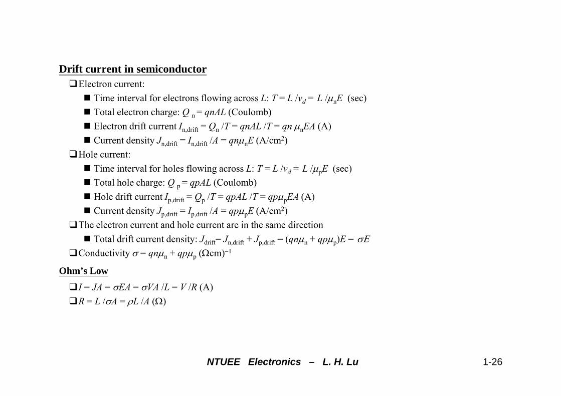
Drift current in semiconductorElectron current: Time interval for electrons flowing across L: T = L /vd = L /nE (sec) Total electron charge: Q n = qnAL (Coulomb) Electron drift current In,drift = Qn /T = qnAL /T = qn nEA (A) Current density Jn,drift = In,drift /A = qnnE (A/cm2)
Hole current: Time interval for holes flowing across L: T = L /vd = L /pE (sec) Total hole charge: Q p = qpAL (Coulomb) Hole drift current I d if = Q /T = qpAL /T = qp EA (A) Hole drift current Ip,drift Qp /T qpAL /T qppEA (A) Current density Jp,drift = Ip,drift /A = qppE (A/cm2)
The electron current and hole current are in the same direction Total drift current density: Jdrift= Jn,drift + Jp,drift = (qnn + qpp)E =
Conductivity = qnn + qpp (cm)1
Ohm’s Low
I = JA = EA = VA /L = V /R (A)R = L /A = L /A ()
NTUEE Electronics – L. H. Lu 1-26
Carrier diffusionDiffusion is a manifestation of the thermal random motion of particles. Section I: total # = 6 (3 moving to the left and 3 moving to the right) Section II: total # = 4 (2 moving to the left and 2 moving to the right) Net flux: 1 moving across the interface from section I to section II.
Statistically, a net carrier flow from high to low concentration region in a inhomogeneous material.I II
dxdpqDJ pdiffp )(
dnDJ
Einstein Relation: Dp /p = Dn /n = kT/q = VT (thermal voltage).Total diffusion current densityBoth electron and hole diffusion contribute to current conduction.Total diffusion current density:
NTUEE Electronics – L. H. Lu 1-27
dxdpqD
dxdnqDJJJ pndiffpdiffndiff )()(
dxdnqDJ ndiffn )(
Dn: diffusion constant (diffusivity) of e
Dp: diffusion constant (diffusivity) of h
Graded semiconductorFor a non-uniform semiconductor, the doping concentration is represented as ND(x).The mobile carrier will diffuse due to the non-uniform distribution.The uncompensated space charge will build up a field (potential) for the system to reach equilibrium.No net current flows at any point under equilibrium. Therefore, the built-in potential can be derived under thermal equilibrium
between points with different doping concentration.
Built-in potential from hole concentration
Built-in potential from electron concentration
x
n(x)
Electron diffusion
NTUEE Electronics – L. H. Lu 1-28
dxdV
dxdp
pVE T
dxdpDEp pp
pdpVdV T
0dxdpqDEqpJ ppp
TVVepp /21
212
11221 ln
ppVVVV T
TVVenn /21
21
dxdV
dxdn
nVE T
dxdnDEn nn
ndnVdV T
0dxdnqDEqnJ nnn
1
21221 ln
nnVVVV T
ND(x)E = 0
x
Electron diffusion
Electron drift
E
excess negativemobile charge
excess positivefixed charge
n(x)
ND(x)
1.10 The pn Junction with Open-Circuit Terminals
Physical structure of a pn junctionClose contact of a n-type semiconductor and a p-type semiconductorA two-terminal electron device with anode and cathode
pn-junction in contact
Majority carriers are crossing the interface (diffusion) and recombined in the other side of the junction.Leaving uncompensated space charges ND
+ and NA depletion region.
In depletion region, electric field (potential) builds up due to the uncompensated space charges.The built-in potential behaves as an energy barrier, resulting in reduction of the majority carrier diffusion.This field will also result in minority carrier drift across the interface in the opposite direction to diffusion.
NTUEE Electronics – L. H. Lu 1-29
p-type: doping concentration: NAmobility p
n-type: doping concentration NDmobility n
pn-junction formation (thermal equilibrium)Depletion region increases due to majority carrier diffusion across the junction.The built-in potential from uncompensated space charge increases, resulting in reduction of diffusion.Minority carriers are swept across the junction in the presence of the built-in field drift current.Equilibrium is reached when Jdiff and Jdrift are equal in magnitude and opposite in direction.No net current flows across the junction.
n-type (ND)p-type (NA)E
hole diffusionJp = 0
NTUEE Electronics – L. H. Lu 1-30
NeutralRegion
NeutralRegion
DepletionRegion
hole drift
electron diffusion
electron drift
p
Jn = 0
20
0
0
00 lnlnln||
i
DAT
n
pT
p
nT n
NNVpp
VnnVV
V0p-type
n-type
The depletion regionStep graded junction (abrupt junction) is used for analysis.Carriers are fully depleted in the depletion region.Neutral region in n-type and p-type outside depletion region.Built-in potential: V0 = VT ln (NAND /ni
Neutral p-type region: Majority carrier pp = pp0 = NA
Minority carrier np = np0 = ni2/NA
Depletion region: n = 0 p = 0 p 0
No net current flows across the junction
NTUEE Electronics – L. H. Lu 1-32
1.11 The pn Junction with an Applied Voltage
Depletion regionForward bias: VF reduces the depletion region and the energy barrier.Reverse bias: VR increases the depletion region and the energy barrier.
Charge density (v)
xnxp
qND
x
Charge density (v)
xnxp
qND
x
Forward bias (V = VF) Reverse bias (V = VR)
SipASinD xqNxqNE //max
NTUEE Electronics – L. H. Lu 1-33
qNA
Electric field ()
xnxp
Emax
x
x
Electrostatic potential (V)
xnxp
V0+VR
qNA
Electric field ()
xnxp
Emax
x
x
Electrostatic potential (V)
xnxp
V0VF
AD
ADSi
NNNN
qVVW
)(2 0
)()(2 0
DAD
ASi
DA
An NNqN
VVNWNN
Nx
)()(2 0
DAA
DSi
DA
Dp NNqN
VVNWNN
Nx
Minority carrier distribution due to junction biasMinority carrier distribution is influenced by the junction biasDiffusion currents exist due to non-uniform carrier distributionJunction bias condition: Zero bias (equilibrium): V = 0 Forward bias: V = VF
The I-V characteristics of the pn junctionThe junction current depends on the junction voltageThe junction current is proportional to the junction areaThe junction current is given by
Saturation current:
NTUEE Electronics – L. H. Lu 1-35
)()()()(
spn
nppn LL
An
n
Dp
pi
n
pn
p
nps NL
DNL
DqAn
LnD
LpD
qAI 200
)1( / kTqVs eII
Reverse breakdownBreakdown voltage: a reverse junction bias VR = VZ
A large reverse current flows when reverse bias exceeds VZ
For breakdown voltage < 5V Zener breakdown.For breakdown voltage > 5V avalanche breakdown.Breakdown is nondestructive if the power dissipation is limited.
Zener breakdownThe strong electric field in the depletion region breaks covalent bonds, generating electron-hole pairs.Generated electrons are swept into the n side and holes are swept into the p side for a reverse current.Zener breakdown normally takes place for pn junction with high doping concentrationZener breakdown normally takes place for pn junction with high doping concentration.
Avalanche breakdownThe minority carriers that cross the depletion region gain sufficient kinetic energy due to the field.The carriers with high kinetic energy break covalent bonds in atoms during collision.More carriers are accelerated by the field for avalanche reaction.Avalanche normally takes place first for pn junction with low doping concentration.
NTUEE Electronics – L. H. Lu 1-36
1.12 Capacitive Effects in the pn Junction
Depletion or junction capacitanceThe depletion width is controlled by the terminal voltage.The change of terminal voltage (dV) will result in dQ at the
edge of the depletion region capacitance.The junction capacitance due to space charge is Cj = dQ/dVR.
Cj can also be estimated by a parallel-plate capacitor:
0 )(2 VVNNW RADSi
AD
AD
R
Si
R
nD
Rj NN
NNVV
VqAdV
wqANddVdQC
)(2 0
0
Under forward bias conditions, W reduces larger Cj.Under reverse bias conditions, W increases smaller Cj.General formula for depletion capacitance for arbitrary doping profile:
NTUEE Electronics – L. H. Lu 1-37
00
00
0
0
12
112
)(
VNNNNqAC
VVC
VVNNNNqA
wAC
NNq
DA
DASij
Rj
RDA
DASi
dep
Sij
RAD
mRjj V
VCC )1(0
00
Diffusion capacitanceExcess minority carrier stored in neutral region will change with the terminal voltage capacitance.By integration the excess minority carriers at both sides:
Small-signal diffusion capacitance:
IIIIDLI
DL
QQQ Tnnppnn
np
p
pnp
22
IVdV
dQC
eIeIIQ
T
Td
VVsT
kTqVsTT
T
)(
//
Cd is large under forward bias conditions.Cd is neglected under reverse bias conditions.