Electroosmotic Flow Characterization and Enhancement in PDMS Microchannels by Zeyad Almutairi A thesis presented to the University of Waterloo in fulfillment of the thesis requirement for the degree of Master of Applied Science in Mechanical Engineering Waterloo, Ontario, Canada, 2008 c Zeyad Almutairi 2008
Transcript
Electroosmotic Flow Characterizationand Enhancement in PDMS
Microchannels
by
Zeyad Almutairi
A thesispresented to the University of Waterloo
in fulfillment of thethesis requirement for the degree of
I hereby declare that I am the sole author of this thesis. This is a true copy of the thesis,including any required final revisions, as accepted by my examiners.
I understand that my thesis may be made electronically available to the public.
ii
Abstract
Electroosmotic flow is widely used as a solution pumping method in numerous mi-crofluidic applications. This type of flow has several advantages over other pumpingtechniques, such as the fast response time, the ease of control and integration in differ-ent microchannel designs. The flow utilizes the scaling of channel dimensions, whichenhances the effects of the electrostatic forces to create flow in microchannels under anelectrical body force. However, the electrostatic properties of the solution/wall materialpairings are unique and must be experimentally measured. As a consequence, accurateknowledge about the electrostatic properties of the solution and wall material pairingsis important for the optimal design of microfluidic devices using electroosmotic flow.Moreover, the introduction of new solutions and new channel materials for differentapplications is common in the microfluidics area. Therefore, any improvement on theexperimental techniques used to examine the electrostatic properties of microchannels isbeneficial to the research community.
In this work, an improvement to the current-monitoring technique for studying theelectrokinetic properties of microchannels is achieved by replacing the conventionalstraight channel design with a new Y-channel design. The errors from both the unde-sired pressure driven flow and solution electrolysis were addressed and significantly re-duced. The new design offers high accuracy in finding the electrokinetic properties ofmicrochannels. The experimental outcome from the new channel design is better com-pared to the outcomes of the straight channel, which helps in distinguishing the importantelectroosmotic pumping regions from the current-time plot. Moreover the time effective-ness in performing the experiments with the new channel design is better compared tothat for the straight channel design.
A modified analysis approach is also presented and validated for finding the elec-trokinetic properties from the outcomes of the current-monitoring technique, which iscalled the current-slope method. This approach is validated by comparing its findingswith the results of the conventional length method. It was found for most situations thatthe discrepancy between the two methods, the current-slope and total length method,are within the uncertainty of the experimental measurements, thus validating the newanalysis approach. In situations where it is hard to distinguish the start and end of so-lution replacement from the current-time plot of the current-monitoring technique, thecurrent-slope method is advised.
With the new design, different parametric studies of electroosmotic flow in PDMSbased microchannels are estimated. At first the zeta potential of biological buffers arestudied. Moreover the effect of continuous electroosmotic pumping, the chip substrate
iii
structure, and temperature on the average zeta potential of microchannels are examined.It was found that for air plasma treated PDMS microchannels the chip substrate materialdoes not have an effect on the average zeta potential of the microchannels.
The following chemical treatments are attempted with the aim of improving the sur-face and electrostatic properties of PDMS based microchannels: prepolymer additivewith acrylic acid, extraction of PDMS, and both heat and plasma induced HEMA (Hy-droxyethyl methacrylate) grafting on the surface of PDMS. Extensive characterization isperformed with different experimental methods. The stability of the artificial hydrophilicproperties of the PDMS microchannels with time was improved with both the extractionand HEMA grafting techniques. On the other hand, there was no evidence of any im-provement in the zeta potential of microchannels with the surface treatments.
iv
Acknowledgements
In the name of God the most gracious the most merciful.
First I would like to thank both of my supervisors Prof. Ren and Prof. Johnson fortheir help and support during my quest for the master degree. The research attitude, andthe encouragement from Prof. Ren has changed my research approach to a better stateand are well appreciated. My sincere gratitude to Prof. Johnson for his professionaladvises and ideas regarding my research. At one point during the master program hestood by my side and helped me to overcome serious problems that were hindering myprogresses in the research. I’m very grateful to him.
I would like to thank Prof. Culham and Prof. Yarusevych for agreeing to be thecommittee members of the MSc degree. Their comments and suggestions have helped inimproving the thesis structure.
Special thanks to Prof. Leonardo Simon from the chemical engineering departmentfor his assistance, discussion and support with the ATR-FTIR system. Also thanks andappreciation to Prof. P. Chen from the chemical engineering department for allowing theuse of his contact angle measurement system.
Special appreciation is directed to the group members at the Microfluidics lab at theUniversity of Waterloo. Lab members that I worked closely with and deserve recognitionare Tom Glawdel, Razim Sami, Jay Taylor, and Sean Wang.
I would like to thank my sponsor King Saud University for their financial supportduring my graduate studies. Also I wish to thank the Saudi Cultural Bureau in Canadafor their endless efforts for assisting the Saudi students in Canada. Their work is in theshadow and I would like to thank them for it.
Special thanks for my dear friends here in Waterloo who made the work in last twoyears somewhat enjoyable. I gained great friends that I would like to dedicate themwith special appreciation whom are Mubarak Almutairi (My Cousin), Fawaz Alsolami,Abdulaziz Alkhoraidly, Ammar Altaf and Khalid Almutairi.
Last but not least, I would like to thank my dear family who supported and encour-aged me to stay with my choices. Special appreciation and respect to my father, who ismy main inspirer. He raised me on looking for the hard path, pursue new adventures,and not to be short-sighted about different issues. Sincere appreciation to my mother,since her love and support was there when I need it. I’m indebted for the affection of mysiblings, especially my younger sister Tahani.
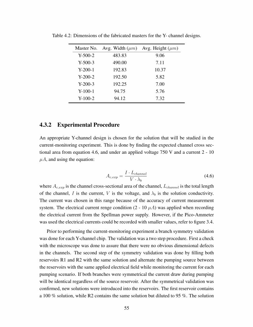
4.2 Dimensions of the fabricated masters for the Y- channel designs. . . . . 55
4.3 The effect of changing the channel dimensions on the zeta potential for1X TBE buffer and PDMS/glass chip. . . . . . . . . . . . . . . . . . . 60
4.4 The zeta potential values for different solutions for the Y-channel andstraight channel results found in the literature. (∗) is from experimentsperformed in the lab with a straight channel design. . . . . . . . . . . . 62
5.1 Results of PDMS/SU8 microchannels with different solutions and differ-ent Y-channel designs. . . . . . . . . . . . . . . . . . . . . . . . . . . 70
5.2 Temperature effects on the zeta potential for different solutions. . . . . 73
6.2 Infrared frequencies and the assigned chemical compounds [85] . . . . 85
6.3 Results of the current-monitoring exepriments and the dry storage anal-ysis for different HEMA grafting protocols. P/P is the PDMS/PDMSmicrochannel, and P/g is the PDMS/glass microchannel. . . . . . . . . 92
C.1 Uncertainty parameters of the experimental setup. . . . . . . . . . . . . 112
4.8 The electrolysis phenomena and its effects on the solutions at the reser-voirs during electroosmotic pumping. . . . . . . . . . . . . . . . . . . 53
Aab Absorbance of infra red beamAc Microchannel cross sectional area (m2)
Ac exp Expected microchannel cross sectional area (m2)
cp Specific heat of the solution (J/kg ·K)
xv
ci Molar concentration of species i (mol/L)C Concentration of chemical compound (mol/L)Clight Speed of light (m/s)Di Diffusion coefficient of species i (m2/s)
Dh Hydraulic diameter of microchannel(
=4 · Ac
P
)e Electron charge (C)~E,E Applied electric field (V/m)Ex, Ey, Ez Applied electric field at different coordinates (V/m)Es Streaming potential (V)f Form factor of channel or capillary (m−1)~Fb External body force in vector notation (N/m3)h Channel height (m)I Electrical current (A)I1, I2 Steady current values at the start and end of replacement (A)Ibulk cond Current carried from the bulk conductivity of the solution (A)Isurf cond Surface current carried within the EDL (A)Itotal Total current draw during electroosmotic flow (A)k Spring constant (N/m)kb Boltzmann constant (m2kg/s2K)
l Path length of the infra red beam (m)L Channel length (m)Lchannel Total channel length (m)Ld Displacement length in the microchannel in the Y-channel design (m)Lside Side channel length of the Y-channel design (m)m Mass (kg)M Solution concentration (mol/L)ni Ionic numberni∞ Ionic concentration at natural stateP Channel perimeter (m)4p, ~p Pressure (Pa)Re Reynolds numberRelectrical Electrical resistance of the solution in the microchannel (Ohm)Ri Rate of generation of species i due to chemical reactionR1, R2 Meniscus radius (m)R1, R2, R3 Reservoirs of the microchannelt1, t2 Start and end of replacement times (s)4t Time difference (s)
xvi
T Absolute temperature in kelvin (K)~T Temperature field (K)Ttran Transmittance of infrared beam~u Velocity field (m/s)uav Average velocity in microchannel (m/s)uslip Slip velocity at shear layer in the EDL (m/s)uemo Average electroosmotic velocity in the microchannel (m/s)w Channel width (m)W Wave number (cm−1)zi Valence of ion specie i
)φ Applied electric potential (V olt)κ−1 Debye length (m)λb Solution conductivity (S/m)λs Surface conductance (S - Siemens)ω Frequency of vibration (Hz)ψ Electrostatic potential from the surface charge (V olt)µ Solution viscosity (Pa · s)µemo Electroosmotic mobility (m2/V · s)ρ Solution density (kg/m3)ρf Charge densityσ Fluid surface tension (N/m)σsg Solid-gas interfacial energy (N/m)σsl Solid-liquid interfacial energy (N/m)θ Contact angle (Degree)ζ Zeta potential (V olt)
xvii
Chapter 1
Introduction
1.1 Background
The area of microfluidics has attracted an increased interest in recent years from re-searchers in chemistry, biomedical and engineering sciences [1, 2, 3, 4, 5]. The areaattracted research since it offered different features that are beneficial for many appli-cations [1, 2, 3, 4, 5]. Controlling the environmental domain in microdevices, such asthe mass flow, and temperature, can be achieved with high precision [4, 5]. Moreover,reducing the volumes of reagents, shortening the experimental time, and increasing thedetection accuracy are reasons for the interest in microfluidics [4, 5].
Microfluidics is a multidisciplinary field where researchers combine their efforts tosuccessfully manufacture devices for desired applications [5]. The design of microflu-idic devices may require the integration of different physical phenomena and will gothrough stages (such as device analysis, numerical simulations, prototyping, and valida-tion studies) before the final micro device is produced. Currently the micro total analysis(µTAS) has the largest research interest, where different applications are integrated andoptimized in one chip [1, 3, 5]. The fabrication of a successful µTAS-chip for an appli-cation may involve: flow pumping, reagent mixing, flow control, and detection processes[5]. The µTAS analysis is also referred to as Lab-on-Chip. The main applications forresearch in Lab-on-Chip are in biomedical diagnostics.
The global market for technologies related to the microfluidics area was approx-imated to be 3 billion dollars in 2006, and it is expected to grow [1, 3]. The mainarea of research is the Lab-on-Chip applications which are related to the health sciences[1, 3, 6, 7]. The objective is to successively manufacture chips that will perform differentbiomedical analyses with high accuracy and short operation time. However, other areas
1
related to microfluidics, such as chemical synthesis and sensors, also received a largeinterest [1, 2, 5, 8, 9].
Throughout the applications of microfluidics, electroosmotic flow is extensively usedin various functions, such as sample transport, micromixing, and reagent delivery [4, 10].Various aspects of electroosmotic flow such as the ease of control, fast response time, andease of integration, are reasons that attracted researchers to use it in numerous applica-tions [4, 10]. Electroosmotic flow can be created in microchannels since the effects ofelectrostatic forces are increased in the microscale, and under an applied electric fieldflow is achieved. As a consequence, accurate knowledge about the electrostatic prop-erties of the solution and wall material pairing is important for the optimal design ofmicrofluidic devices using electroosmotic flow [4, 10].
As microfluidics evolves, different channel material and new solutions are frequentlyintroduced in numerous applications. One example is polydimethylsilicone (PDMS),which is an elastomeric polymer widely used as a microchannel substrate material be-cause of the ease and cost of manufacturing. Also, PDMS supports electroosmotic pump-ing in microchannels. However, the electrostatic properties of PDMS are lower than thatof glass or silicon. PDMS also has several disadvantages, such as the hydrophobic na-ture and the sample adsorption, which hinder the use of PDMS in different microfluidicapplications. Thus, the area of treating PDMS for different applications has gained aninterest from different researchers with an aim of improving the electrostatic propertiesof PDMS.
1.2 Research Motivator
In different microfluidic applications electroosmotic flow is used as a pumping tech-nique to drive fluid and transfer species through channel geometries [4, 10]. Electroos-motic flow utilizes the geometrical scaling effects of microscale channels which willenhance the effects of electrostatic forces [4, 10]. To this end, different experimen-tal techniques are available to study different electrostatic properties of microchannelwalls and solutions, and the most common technique in the microfluidics communityis the current-monitoring technique. If correctly used, the current-monitoring techniqueis simple and reliable. However, for microchannels in chip format the technique hassome practical weaknesses that will affect its results. Problems such as the solution elec-trolysis and undesired pressure driven flow can cause errors from the outcomes of thecurrent-monitoring technique.
In the first part of the thesis the improvement on the current-monitoring technique is
2
presented with the use of a new Y-channel design. Also, a modified analysis approach,the current-slope approach, for the experimental outcomes of the current-monitoringtechnique is presented and validated.
In the microfluidic area, PDMS is widely used for different applications as a channelmaterial in devices utilizing electroosmotic flow. PDMS is hydrophobic and has lowelectrostatic properties (the zeta potential ζ), compared to glass. For these reasons, thesecond motivator for this work is the enhancement of the electroosmotic flow and surfaceproperties of PDMS based microchannels. Different chemical based surface treatmentsare attempted and a full scope characterization is done with experimental approaches.
1.3 Objective and Outline
The general scope of the thesis is divided into two main parts, first the study of the elec-trostatic properties of biological buffers in PDMS based microchannels, and second theenhancement of the electrostatic and surface properties of PDMS based microchannels.The main goals of this work are as follows:
1. Develop a simple and reliable channel design and improved experimental approachto study the electrostatic properties of microchannels.
2. Propose a new analysis approach, the current-slope approach, for the outcomesfrom the current-monitoring technique.
3. Measure the electrostatic properties of different biological buffers, MOPS, L15-ex,and HEPES, that have not been reported in the literature.
4. Perform different parametric studies on the electroosmotic flow in microchannelsto find the effects of changing the experimental conditions on electroosmotic flowin PDMS microchannels.
5. Enhance the surface electrostatic properties of PDMS based microchannels withchemical treatments.
6. Perform a characterization study of the effects of the chemical treatments on thehydrophilic and zeta potential properties of PDMS based microchannels
The thesis is outlined as follows:
3
Chapter 2: An overview of the theory and basic concepts of microfluidics is presented.The chapter will also include a literature review on both the current-monitoringtechnique and the surface treatment of PDMS based microfluidic chips.
Chapter 3: The experimental setups used in this work will be presented in this chap-ter. Mainly, the solutions used, the chip and sample manufacturing, the current-monitoring setup, the contact angle system, the ATR-FTIR system, and the fluo-rescence microscopy system are discussed.
Chapter 4: In this chapter the new Y-channel design will be presented to study the elec-trostatic properties of microchannels with the current-monitoring technique. Thedifferent aspects of the design will be discussed. Moreover, the validation of theaccuracy of the Y-channel design with different criteria will be examined.
Chapter 5: The chapter will first present the modified current-slope approach that wasproposed for analyzing the outcomes of the current-monitoring technique. Also,different parametric studies on electroosmotic flow in PDMS microchannels willbe presented.
Chapter 6: This chapter will discuss the different chemical based surface treatmentsused to modify and enhance the electrostatic properties of PDMS based microchan-nels. The characterization of the effects of the treatments will be presented withdifferent experimental studies.
Chapter 7: In this chapter a summary of the results that were reached in the presentwork will be presented. Recommendations for further improvements on the currentstudies will also be presented.
4
Chapter 2
Literature Review
The design of microfluidic applications requires an understanding of physical phenomenain microscale [1, 3, 11, 8, 6, 7]. Due to dimensional scaling, certain phenomena diminishsuch as the convective momentum and the gravity force compared to others like theviscus and electrostatic forces. First a view of the different applications of microfluidicswill be presented. A general overview of different transport phenomena in microscaleis discussed in this chapter with the emphasis on the momentum transport phenomena.Also, the use of PDMS as a channel substrate material is discussed. Furthermore, thesurface modifications that have been used to maintain desirable surface properties inPDMS based microchannels are reviewed.
2.1 Microfluidics Background
Microfluidics can be defined as the study of the transport and control of minute volumesof fluid in small scale devices [1]. The area was introduced following the establishment ofMEMS (Microelectromechanical systems), which allowed manufacturing microchannelswith high accuracy [1]. Microfluidics gained interest in different bio-medical diagnosticsand chemical synthesis research because of its promising advantages such as handlingminute samples, increasing the detection accuracy, and reducing the time needed to per-form experiments were reasons that attracted research to microfluidics [5, 8, 12, 13, 14].Moreover the ability and precision in controlling the experimental environment, such astemperature and flow rate, were other reasons for this interest [2, 5, 8, 6, 7, 15]. Themicrofluidics area is also facing great challenges, such as material challenges, flow con-trol, mixing, and cost of devices [2, 5, 8]. Up to now most of the research that has beendone in microfluidics is still in the proof of concept stage and validating its use in dif-
5
ferent applications [1, 5, 8, 13]. However, it is anticipated by numerous researchers thatin the near future devices with microfluidic concepts for biomedical and life sciencesapplications will be available [1, 2, 5, 8, 7, 14].
Lab-on-Chip is the area that is concerned with studying and promoting the appli-cation of microfluidic concepts in biomedical applications [5, 7]. Microchip devices,such as cell sorter, cell culture, DNA, and protein separation and analysis, are examplesof Lab-on-Chip devices [14, 16, 17, 18, 19, 20, 21]. Presently Lab-on-Chip applica-tions is the area that has the highest attraction for research in microfluidics [5, 15]. Thefuture goal of Lab-on-Chip is developing portable biomedical diagnostics devices withhigh accuracy and short analysis time. Achieving this goal needs cooperation betweenresearchers from different scientific disciplines and it will involve the optimization ofdifferent physical phenomena.
An example of a micro device that is considered as a Lab-on-Chip device was pre-sented by Dodge et al. [22]. The main operation of the chip was to isolate myoglobin,a single chain protein, from a bio-sample. The system involved the integration of flowcontrollers, pumps, and micromixers [22]. Another example for microfluidics applica-tion in the bio-medical area is the PCR chip (polymer chain reaction) for DNA. The PCRtechnique amplifies a DNA sample with heat controlled reactions. This is performed inmicrofluidic chips since precise temperature control and variation can be achieved withhigh precision [17, 18, 23]. Recently, Lui et al. [23] was able to integrate a chip withITP-ZE (Isotachophoresis-Zone electrophoresis) to separate the Hepatitis B virus withhigh accuracy that competed with the accuracy of conventional macro devices [23].
Agilent Technologies successively produced a commercial product which was basedon microfluidic concepts. The Agilent HPLC-chip is a microfluidic chip that is used alongwith the Agilent 2100 bioanalyzer to perform liquid chromatography of bio samples. TheHPLC-chip is polymeric based and reusable. Agilent states that the accuracy and the timefor performing measurements with this chip are better than conventional methods [24].
In chemical synthesis applications, the microfluidics area is also promising since theprecision of controlling the mass and thermal transport are high in the microscale [2, 8,9, 12]. An example of a successive chemical synthesis application in microfluidics waspresented by Miller et al. [12]. They successfully performed a carbonylation reaction ina glass microchip. This type of reaction in macro scale needs high pressure and specialconditions, yet it was achieved in microscale with a reaction rate higher than that of amacroscale domain [12].
The first era of microfluidics started with microchips fabricated from glass and sili-con. The fabrication process was time consuming and expensive [1, 3]. The introduction
6
of polymeric based materials to the microfluidics area was the period for which the re-search in microfluidics gained a lot of interest because of the simplicity and cost ofmanufacturing the chips. PDMS (polydimethylsilicone) is one polymeric material thatattracted the attention of researchers because of its favorable properties that suit differ-ent microfluidic applications. On the other hand, PDMS needs to be treated for certainapplications, as will be discussed later in this chapter.
Initially, microchips for microfluidic applications were fabricated from glass and sili-con. The fabrication process was time consuming and expensive [1, 3]. The introductionof polymeric-based materials to the microfluidics area attracted a huge interest becauseof the simplicity and low cost of manufacturing the chips. PDMS (polydimethylsilicone)is one polymeric material that attracted the attention of researchers because of its favor-able properties, such as optically transparent, ease of manufacturing, and low cost, whichsuits different microfluidic applications. On the other hand, PDMS needs to be treatedfor certain applications, as will be discussed later in this chapter.
For an integrated microfluidic chip, different processes may be incorporated and op-timized in a single chip, such as sample transport, flow control, temperature control, andeffective mixing [1, 2, 3, 8]. These goals are achieved by an understanding the transportphenomena of fluids in microscale [1, 2, 3, 8].
2.2 Microscale Transport Phenomena
An understanding of transport phenomena of mass, momentum, and heat in microscale isimportant for the design of microfluidic devices. In the literature there are several booksthat cover different transport phenomena in microfluidic applications [1, 3, 4].
For the liquid phase in a microchannel, the continuum approach is still valid as longas the characteristic length of the microchannel is large compared to the mean free pathof the fluid molecules [1, 3, 4, 11, 8] 1. This is the case for most microfluidic devices, andfor the work that will be discussed in this thesis. Thus, the established macro scale mass,momentum, and energy conservation equations are appropriate to analyze the microflu-idic systems. Moreover, solution properties, such as viscosity, density, and electricalconductivity are assumed to be identical to the values used in the macro scale analysis.
1The Knudson number relates the mean free path between the molecules of the fluid with the charac-teristic length of flow domain. The Knudson number gives a direction on how to analyze the fluid flow andif the continuum approach is valid. It is very important for gas dynamic analysis since the intermoleculardistance of the gas molecules are higher than of liquids [3].
7
Due to the scaling of geometry and the large surface to volume ratio of channels, dif-ferent phenomena will have considerable effects on the flow. First, the Reynolds number(Re) in microchannels is around unity and the flow is laminar [1, 3]. As a consequence,viscous forces play a significance role in the flow. Also, the mixing speed of non re-acting solutions is low in the microscale, since the dominant mixing mechanism is thediffusion of the species [1, 3, 25]. Moreover, the electrostatic effects become significantin microscale. This comes in the formation of the electric double layer (EDL) of ions in aregion close to the wall of the microchannel. Body forces also change in the microscalewith the gravity effects diminishing compared to the electrostatic and capillary forces[1, 3, 4]. Electrostatic effects play a major role in flow development in microscale suchas electroosmotic flow and electrophoreses [4, 11].
2.2.1 Electric Double Layer (EDL)
When a channel surface comes in direct contact with a solution that has polar propertiesand in the absence of chemical reactions, a static surface charge will build along the wall[4, 11, 26]. This build up of the electric potential can occur due to different chemicalmechanisms, such as ionization of surface groups, specific ionic absorptions on the wall,or other mechanisms [4, 11, 3]. This surface charge will affect the solution ions. Theions that have the opposite charge of the wall will be attracted and the ones having thesame charge as the wall will be repelled. This phenomenon takes place to neutralizethe wall surface charge. The region close to the wall where the wall surface charge isaffecting the solution ions is called the electric double layer (EDL). Figure 2.1 presentsa schematic of the EDL.
Figure 2.1: The electric double layer (EDL) [11].
8
As presented in Figure 2.1 there are two distinct regions in the EDL: a region con-taining immobile ions (stern layer), and the diffuse layer. The stern layer is the regionwhere the ions are firmly attracted to the wall. The diffuse layer is the region in whichthe ions have some mobility of motion, such as diffusion, while still being affected bythe wall charge. The thickness of the EDL is approximated to be in the same order as theDebye length [4, 11, 3]:
κ−1 =
(ε · kb · T
2 · e2 · z2i · ni∞
)1/2
(2.1)
where κ−1 is the Debye length, ε is the solution permittivity, kb is the Boltzmann con-stant, T is the absolute temperature, zi is the valance of the species i, e is the electroncharge, and ni∞ is the ionic concentration at natural state. The Debye length for a sym-metric electrolyte with a valance of z+ = −z− = z at a temperature of 25oC can beapproximated by [11]:
κ−1 =3.04
z ·√M× 10−10 (2.2)
where M is the solution concentration in mol/L. Equation 2.2 suggests that thicknessof the EDL will decrease as the solution concentration increases because more ions areavailable to neutralize the wall surface charge.
The analysis of the electric potential carried within the EDL is important since it is abody force in the microscale cannot be neglected. To find the effect of applying an ex-ternal body force on the EDL, the charge distribution of the ions in the EDL region mustbe found. The analysis of the electric charge potential follows the derivation presentedin the literature [4, 11, 26]. It is assumed that the ionic distribution for a certain speciesfollows a Boltzmann distribution and is presented by [4, 11, 26]:
ni = ni∞ exp
(−zieψ
kbT
)(2.3)
where ni is the ionic concentration of species i, ni∞ is the ionic concentration at neutralstate (ψ = 0), zi is the valance of the ion, e is the charge of the electron, ψ is theelectrostatic potential distribution from the wall, kb is the Boltzmann constant, and T isthe absolute temperature. The ionic charge density is found by:
ρf =∑
i
e · zi · ni (2.4)
where ρf is the charge density of the ions. By assuming that the electric charge distribu-tion is only affected by the wall charge equation 2.4 will reduce to:
ρf = −2 · e · zini∞ · sinh
(zieψ
kbT
)(2.5)
9
The electrostatic potential distribution within the EDL could be found from the Poissonrelation:
d2ψ
dy2= −ρf
ε(2.6)
d2ψ
dy2=
2 · e · zini∞
ε· sinh
(zieψ
kbT
)(2.7)
For a thin EDL the hyperbolic term will reduce to the first term of the Taylor expansion[3]:
sinh
(zieψ
kbT
)'
(zieψ
kbT
)(2.8)
Thus, the electrostatic potential reduces to:
d2ψ
dy2= κ · ψ (2.9)
One important property of the EDL is the electrostatic potential at the imaginary shearplane in the EDL (figure 2.1 which is called the zeta potential ζ . The zeta potential isimportant since it relates the average electroosmotic pumping in microchannels with theapplied electrical field, as will be presented in the an upcoming section [4, 11, 26].
When an external electrical body force is applied tangentially to the EDL, the mobileions in the diffuse region of the EDL will move with a non uniform velocity distributionacross the EDL thickness. This can be used as for solution pumping since the bulksolution in the region out of the EDL will be dragged by viscous forces. More details onthis phenomenon will be presented in explaining the electroosmotic flow.
2.2.2 Thermal Transport
The thermodynamic state of a control volume in a microchannel is governed by the en-ergy balance described previously in the literature for macro scale but with some modi-fications [1, 3, 8]. The energy conservation equation is presented next:
ρ · cp[∂T
∂t+ ~u · ∇~T
]= ∇ ·
(k (T ) · ~T
)+ λb (T ) · ~E · ~E (2.10)
where ρ is the solution density, cp is the specific heat of the solution, ~T is the absolutetemperature field, λb (T ) is the solution conductivity as a function of temperature, and ~E
is the applied electrical field. Due to scaling of the geometry the surface to volume ratioin microchannels is very high and the heat dissipation is large [1, 12]. This improves
10
precision in controlling the heat in the microscale domain [1, 8] and has been utilizedin different microscale applications that need precise temperature control, such as PCRchips.
An important phenomenon that has crucial effects on the stability of electroosmoticpumping is the joule heating [27]. This phenomenon happens since the solution that isbeing pumped has an electric conductivity which will create an electric current. Thus, thepresence of both the electrical current and the applied voltage creates internal heating.This will cause changes in the solution properties, moreover the flow pumping conditionswill change. This will effect the outcome of the electroosmotic pumping. Therefore, itmust be taken into consideration when electroosmotic pumping is used [27]. The finalterm of equation 2.10 is the internal heat generation in the presence of joule heating.
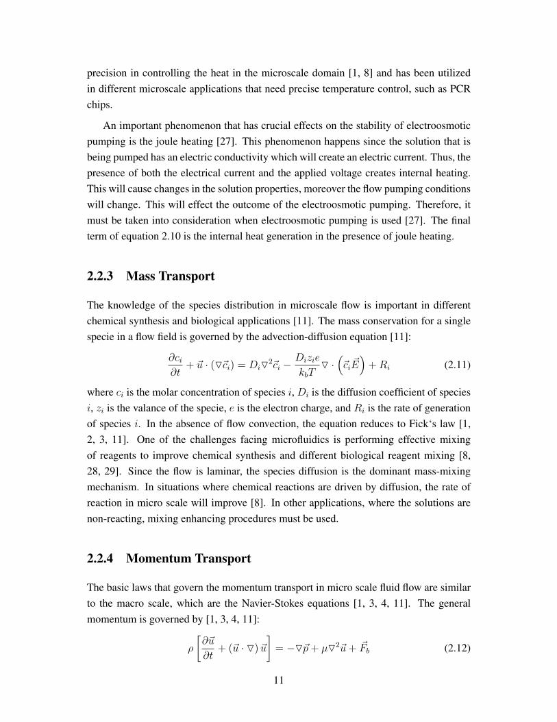
2.2.3 Mass Transport
The knowledge of the species distribution in microscale flow is important in differentchemical synthesis and biological applications [11]. The mass conservation for a singlespecie in a flow field is governed by the advection-diffusion equation [11]:
∂ci∂t
+ ~u · (O~ci) = DiO2~ci −
Dizie
kbTO ·
(~ci ~E
)+Ri (2.11)
where ci is the molar concentration of species i, Di is the diffusion coefficient of speciesi, zi is the valance of the specie, e is the electron charge, and Ri is the rate of generationof species i. In the absence of flow convection, the equation reduces to Fick‘s law [1,2, 3, 11]. One of the challenges facing microfluidics is performing effective mixingof reagents to improve chemical synthesis and different biological reagent mixing [8,28, 29]. Since the flow is laminar, the species diffusion is the dominant mass-mixingmechanism. In situations where chemical reactions are driven by diffusion, the rate ofreaction in micro scale will improve [8]. In other applications, where the solutions arenon-reacting, mixing enhancing procedures must be used.
2.2.4 Momentum Transport
The basic laws that govern the momentum transport in micro scale fluid flow are similarto the macro scale, which are the Navier-Stokes equations [1, 3, 4, 11]. The generalmomentum is governed by [1, 3, 4, 11]:
ρ
[∂~u
∂t+ (~u · O) ~u
]= −O~p+ µO2~u+ ~Fb (2.12)
11
where ρ is the solution density, µ is the solution viscosity, Op is the pressure gradient,and ~Fb is the applied body force. Body forces from gravity effects diminish in the flowfield because of the scaling of geometry 2. Thus, the electrostatic body force and thecapillary effects will have an influence on the flow in microscale and must be considered[1, 3, 4, 10, 11].
In most cases the flow in microchannels is steady and laminar with Re less than unity(Re ≤ 0.1). Thus, the time dependent term will be eliminated. Moreover, the convectionterm in the equation 2.12 could be neglected compared to the viscous term [1, 3]. Thisleads to Stokes’ approximation of the momentum conservation [1, 3]:
0 = −O~p+ µO2~u+ ~Fb (2.13)
The three major pumping methods in microfluidic devices are: pressure driven flow,capillary driven, and electroosmotic driven flow. The main aspects of these methods willbe presented next, with more elaboration on electroosmotic driven flow.
Pressure Driven Flow
Pressure driven flow is achieved by applying a pressure difference between the nodes(reservoirs) of the channel network with the aid of an external pressure source, such assyringe pumps [10]. The velocity field in the channels will have a parabolic profile,identical to the laminar Poiseuille flow profile [1, 3], across the cross section area of thechannel [1, 3], which is unfavorable for sample transport and detection applications [30].This Poiseuille flow profile will increase the sample dispersion and the lower the accuratedetection of the analytes. Also, the need for an external pressure source complicates thehardware setup, and the portability of the devices is affected. Another issue with pressuredriven flow is that immediate flow control is hard to achieve since valving elements arehard to integrate in microchips that use hard materials for channel substrates [1, 3, 31].Thus, different means of flow control in pressure driven flow in microscale is still anopen research problem [31].
Unger et al. [31] utilized the flexibility properties of PDMS microchannels to createpneumatic operated valves in microchips that allowed the control of the flow directionin microchips. The main issue with their system is that the controlling of the valves isachieved with a large external setup, which eliminates the portability of the device [10].
2The gravity force is scaled to the third power while the capillary force is scaled to the first powercompared to the characteristic length . The decrease in the dimensions will reduce the gravity effectscompared to the capillary and electrostatic forces [1].
12
A unique phenomena happens with pressure driven flow in shallow microchannelswhich is the electroviscous effects [4, 11, 26]. When fluid flows in a shallow microchan-nel, and due to the presence of EDL, this flow will cause the free ions in the EDL tomove in the flow directions and accumulates. This accumulation of ions induces a poten-tial field that creates a back flow in the microchannel. To an observer, the flow rate willbe lower than the predicted flow rate from the traditional laminar Poiseuille flow equa-tion. This is analogous to an increase in the viscosity of the solution in the microchannel;hence it is called the electroviscous effect. This effect has been utilized in the streamingpotential technique to find the electrostatic properties of materials.
Capillary Driven Flow
Capillary driven flow uses the surface to volume ratio aspects of microchannels and thesurface energy effects of the wall on the solution to create a passive pumping method.By utilizing the nature of the surface tension from channel walls, fluid flow could beachieved by creating gradients regions of hydrophilic channel patterns in the microchan-nels. This is achieved by creating meniscus shape differences between the two ends ofthe microchannel [1, 3, 32, 33, 34]. The flow in the capillary can be found by:
4p = σ
(1
R1
− 1
R2
)(2.14)
where σ is the fluid surface tension, and R1 and R2 are the solution radius of curvatureof the gas liquid interface. This method of pumping is useful for passive continuouspumping of solutions in microchannels, but the limitations of immediate flow control isstill apparent, similar to pressure driven flow.
In the literature, Berthier and Beebe [32] analyzed the stability conditions of a passivepump utilizing surface tension properties. Suk and Cho [34] used a scheme to patternthe microchannel with hydrophilic and hydrophobic regions to create a flow in the mi-crochannel. Also they studied the effect of the ratio of hydrophilic to hydrophobic areason the flow field [34].
Electroosmotic Driven Flow
Electroosmotic flow is an electrokinetic driven flow that utilizes the presence of the EDLin microchannels [4, 11, 26]. The flow is created by applying an external body force withan electric field that affects the free ions in the EDL causing them to migrate in a certaindirection. The movement of the ions is affected by the sign of the surface charge and the
13
direction of the electric field. The electric field can be implemented by placing electrodesin direct contact with the solution. The migration of the ions within the EDL will causethe solution in the bulk region, away from the EDL, to move with same velocity dueto viscous effects [4, 11, 26]. Figure 2.2 presents a schematic of the principle of theelectroosmotic flow for a negatively charged surface under an applied external electricfield.
- - - - - - - - - - - - -
- - - - - - - - - - - - -
- - - - - - - - -
dydxx
PP ⋅
⋅
∂∂
+dyP ⋅ xbF ,
dxyx ⋅τ
dxdyy
yx
yx ⋅
⋅
∂
∂+
ττ
x
y+ ive- ive
uemo
- -- - - - - - - -
+
Shear planeΨ(y) (Volt)
ζ
- - -- - -+ + + + + + + + + + + +
+ +
++
+
+
+
+
+
+
++
+
+
+
+
++
+
+
+
++
+
++
+
+
+
+
+
+
++
+
+ + +++
++
+++
Diffuse layer
Ψs
++
- ive surface charge
uslip
+ ive
- ive
y
x
y
Microchannel wall
dxdy
++ ++ ++ ++ ++ ++ ++
++ ++ ++ ++ ++ ++ +
Ex
)(Voltφ
Shear plane
- -
h
L
h
w
Flow
direction Applied Body force
Side section
Flow direction
Side View
y
Figure 2.2: Schematic of electroosmotic flow in a microchannel.
The simplicity of incorporating electroosmotic flow in different microchannel de-signs, ease of control through complex channel geometry, and the fast response timeare advantages of electroosmotic pumping which are hard to achieve with other pump-ing methods [4, 10, 11, 26]. Moreover, the velocity profile is plug like, which makesit attractive for sample transport and detection applications. Electroosmotic pumpinghas been widely used in several microfluidic applications such as micromixers [29]; cellsorters [16] , electroosmotic pumps [35], DNA stretching [36], and sample handling andseparation [37, 38, 39]. On the other hand, electroosmotic flow is not without disadvan-tages. Problems, such as the occurrence of solution electrolysis and joule heating undercertain operation conditions, will negatively affect the electroosmotic flow in microchan-nels [27, 40, 41].
The analysis of the momentum transport in is important to understand the velocity
14
flow field during electroosmotic pumping. A representative 2D control volume in so-lution is presented in figure 2.2 where the CV is under the influence of the pressure,viscous and body forces. The external body force originates from the applied electricpotential that will affect the ions in the EDL. As discussed previously, the momentumconservation is governed by [1, 3, 4, 11]:
0 = −O~p+ µ · O2~u+ ~Fb (2.15)
Under the assumption of the absence of pressure gradient, the equation reduces to:
0 = µO2~u+ ~Fb (2.16)
where ~Fb is the body force coming from the effect of the external electric field on thefree ions within the EDL. This body force is calculated by [11]:
~Fb = ρf · ~E (2.17)
where ρf is the ionic charge density in the EDL, and ~E is the applied electrical field invector notation. For a three dimensional applied electrical field:
Ex =∂φ
∂x,Ey =
∂φ
∂y, and Ez =
∂φ
∂z
whereEx, Ey, andEz are applied electric fields in the different directions, and φ is the ap-plied potential between the electrodes. Recall from the EDL explanation, section 2.2.1,the net charge density ρf is related to the electrostatic surface charge by Poisson equa-tion:
∂2ψ
∂y2= −ρf
ε(2.18)
where ψ is the electrostatic potential due to the wall surface charge, and ε is the per-mittivity of the solution. By considering a flow in a microchannel where the electricfield applied in the x-coordinate and the wall surface charge is affecting the ions in y-coordinate, the momentum equation can be reduced to:
d2u
dy2=εEx
µ
∂2ψ
∂y2(2.19)
By following [1, 3, 4, 11, 26] the equation will reduce to:
u =εEx
µ(ψ − ζ) (2.20)
where ζ is the electrostatic potential at the shear plane of the EDL. In the region awayfrom the EDL ψ = 0, and the velocity is equal to the slip-velocity. Thus, equation 2.20will reduce to:
uslip = −εEx
µζ (2.21)
15
equation 2.21 is known as the Helmholtz-Smoluchowski (H-S) slip velocity equation[1, 11, 26]. For a thin EDL compared to the channel thickness the average electroos-motic velocity in the microchannels is approximated by the H-S slip velocity. From thisequation comes the importance of the zeta potential of microchannels since it relatesthe average velocity in the microchannel with electric field. Another commonly usedterm to describe electroosmotic flow in microchannels is the electroosmotic mobility
µemo =−ζ · εµ
which is a regrouping of the zeta potential and the solution properties.
Electrical Current Draw During Electroosmotic Flow During electroosmotic pump-ing there will be an electrical current draw because of the presence of different ion fluxphenomena. By assuming that the channel material is perfectly insulative and no currentis carried within the stern layer of the EDL, the current draw has three main contributors.The main electric current components are: the current carried from the bulk solutionconductivity, the current carried from the convection of the ions within the EDL, andthe current from the diffusion of ions. The current carried from the diffusion of ions isvery small compared to other terms, therefore it is neglected. The total current draw willreduce to the current carried from the bulk solution conductivity and the convection ofions in the EDL. Another terminology used to describe the current carried in the EDLis the surface conductance. Equation 2.22 presents the total current draw due to steadyelectroosmotic pumping of one solution in a microchannel [11]:
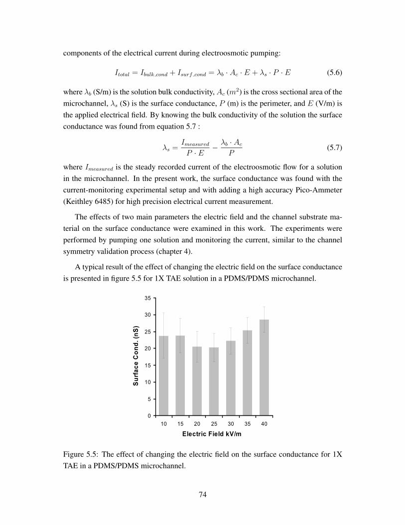
Itotal = Ibulk cond + Isurf cond = λb · Ac · E + λs · P · E (2.22)
where Itotal is the total current draw, Ibulk cond is the current carried from the bulk solutionconductivity, Isurf cond is the current carried within the EDL , λb (S/m) is the solution bulkconductivity,Ac (m2) is the cross sectional area of the microchannel, λs (S) is the surfaceconductance, P (m) is the perimeter, and E (V/m) is the applied electrical field. Sincethe solution conductivity could be measured the surface conductance can be determinedby rearranging equation 2.22 into:
λs =Imeasured
P · E− λb · Ac
P(2.23)
where Imeasured is the steady current recorded during electroosmotic flow in a microchan-nel. In most cases, the current carried within the EDL is small compared to the currentfrom the solution conductivity. Therefore, the measurement of the surface current needsspecial techniques and high precision equipment. Presently, the streaming potential is themost adopted method for finding the surface conductance [11, 26, 42, 43]. Recently, thecurrent-monitoring technique was introduced to estimate the surface conductance duringelectroosmotic pumping [42].
16
2.3 Zeta Potential Measurements
The importance of the zeta potential is that it defines the electroosmotic flow in mi-crochannels where the higher the zeta potential the faster the electroosmotic pumping.The zeta potential by nature is affected by different properties such as wall surface chargedensity, solution concentration, and the pH [44, 45], which makes it unique for the solu-tion and material pairings. Furthermore, due to the nature of the microfluidics area newsolutions and new materials are frequently introduced and the accurate knowledge of thezeta potential of the solution/wall pairing is important when electroosmotic pumping isused.
As an electrostatic property, the zeta potential can not be measured directly. How-ever, it is inferred from the average flow velocity measurements in microchannels, andthen approximated from the H-S equation [4, 11, 44, 45]. Different experimental tech-niques have been used in the literature to find the zeta potential, but the techniques arenot without problems or limitations. The most common experimental methods used tomeasure the zeta potential are as follows: the current-monitoring technique [4, 46, 41,42, 47, 48, 49, 50, 51, 52], the streaming potential [26, 43, 53], and direct velocity mea-surement with micro particle image velocimetry (µ-PIV) and fluorescein photobleaching[46, 54, 21, 51, 55, 56, 57]. These techniques will be presented in the next sections.
2.3.1 Streaming Potential Technique
The streaming potential technique relates the applied pressure difference to the measuredstreaming potential in order to estimate both the zeta potential and surface conductanceof capillary and microchannels [4, 11, 26]. If a solution is forced to flow through achannel with an applied pressure difference, the free ions within the EDL will be carriedin the same direction of the flow, creating a current flow. This current flow is called thestreaming current (Ist). The moving ions accumulate within the EDL, causing an electricpotential to build up, and eventually creating another flow in the direction opposite tothe pressure driven flow. The flow that was created by the induced electric potentialalso carries an electrical current called the conduction current (Icond). If the conductioncurrent and the streaming current are equal (Ist = Icond), then a steady state conditionis reached. The electrostatic potential that is built up at the steady state condition iscalled the streaming potential [26]. By relating the streaming potential and the appliedpressure difference both the zeta potential and the surface conductance could be found[26]. Equation 2.24 presents the relation used to analyze the experimental outcomes of
17
the streaming potential:Es
4p=εζ
µ
1
(λb + f · λs)(2.24)
where Es is the measured streaming potential, 4p is the applied pressure difference,εis the dielectric constant of the solution, λb is the bulk solution conductivity, λs is thesurface conductance, and f is the form factor of the channel or capillary (perimeter /cross sectional area) [26]. Since both the zeta potential and the surface conductance areunknown several measurements must be performed to find a relationship between 4Pand Es. Erickson et al. [43] used this technique to find the zeta potential and surfaceconductance of different solutions in glass. Sze et al. [58] used the technique with themodified slope analysis to find the zeta potential of glass coated with PDMS.
The main issue with this technique is that it needs several points of measurementsin order to get an estimate of the zeta potential. Moreover, the published results in theliterature were not repeatable [43].
2.3.2 Direct Velocity Measurement
Another approach for finding the zeta potential of a microchannel is to quantitativelymeasure the actual velocity in the microchannel. This can be achieved with differenttechniques, such as µ-PIV [54, 56, 59], and fluorescent dye photobleaching [46, 51, 57].Finding the channel zeta potential with direct velocity measurement is not a one step taskand needs some advanced hardware and analysis. Nevertheless, these techniques give ex-tra information about flow field by offering real time flow behavior during electroosmoticflow in microchannels [46, 51, 57].
µ-PIV is a quantitative method used to examine the actual flow field in microchannelsby tracking fluorescent particles introduced in the flow [3]. The velocity field is found bycapturing two consecutive images of the particles in the flow and then performing crosscorrelation analysis to the images to get information about the flow field. After findingthe velocity field from the µ-PIV measurements the zeta potential is found from the H-Sequation 2.21. A point of consideration when using the µ-PIV with the electroosmoticflow is that the particles are mostly charged and the applied electric field will causeparticles to have an electrophoretic motion. Thus, the tracked velocity is made of the twocomponents which are the electroosmotic velocity of the flow and the electrophoreticvelocity of the particles. This issue must be taken with care when analyzing the µ-PIVoutcomes with electroosmotic flow. Yan et al. [54] used the µ-PIV system to find thezeta potential of glass microchannels. The results of the zeta potential were comparableto results found in the literature. Hsieh et al. [59] used a µ-PIV system to find the
18
electroosmotic mobility of square PDMS microchannels and compared the results withresults from the literature.
Another approach is to infer the electroosmotic velocity in a microchannel by tracinga photobleached region in the flow field. This is done by dying the solution with a fluo-rescent dye and then photobleaching a region of interest with an appropriate light source.The photobleached region will have the same velocity as the electroosmotic velocity.The average electroosmotic velocity could be found by tracking the photobleached re-gion. Pittman et al. [46] performed photobleaching of neutral fluorophore to find thesteady electroosmotic mobility in a cross microchannels manufactured in glass and com-pared it to the current-monitoring technique. It was found that the cross intersection willeffect the electroosmotic flow in the microchannel. Wang [57] used the photobleachingtechnique to find the electroosmotic mobility with a glass Y-channel design.
2.3.3 Current-Monitoring Technique
The current-monitoring technique is the most adapted technique in the microfluidic com-munity for finding the zeta potential of microchannels. Figure 2.3 presents a schematicof the operation principle for the current-monitoring technique. The current-monitoringtechnique is based on a simple concept which is monitoring the current change due to thesolution conductivity change while performing electroosmotic pumping [4, 46, 41, 42,47, 48, 49, 50, 51, 52]. This is achieved by replacing the solution that is being pumpedwith the same solution but with a slightly different conductivity (ie. 5 % conductivitydifference). By monitoring the current change with time and finding the time needed toperform the full replacement the average velocity is estimated.
19
Figure 2.3: The basic concept of the current-monitoring technique [19].
The average velocity is found from:
uav =Lchannel
t2 − t1(2.25)
where uav is the average velocity of the electroosmotic pumping in the microchannel,Lchannel is the channel length where the solution is replaced, and t1 and t2 are the startand end times of the replacement process found from the current-time plot. Under theassumption that the EDL thickness is very small compared to the channel characteristiclength the zeta potential could be found from the H-S equation. While it is a qualitativeapproach of monitoring the current change, quantitative values of the zeta potential arefound with very good accuracy. The current-monitoring method offers the simplicityin both the hardware setup and in performing the experiments. Moreover the techniqueallows the zeta potential to be found from one measurement.
Certain conditions apply to the current-monitoring technique to estimate the zetapotential of microchannels, such as the experiment must be performed with the samesolution but with a slightly different conductivity ( 5 % conductivity difference), thepH of the tested solutions must be identical since ζ is pH dependent, and the solutiontemperature must be stable [52].
The first application of the current-monitoring technique was presented by Huanget al. [47] to measure the average velocity of 20mM phosphate buffer in a fused silicacapillary. Soon after, several researchers applied the current-monitoring technique to
20
measure zeta potential in silica and glass capillaries, glass microchannels and polymermicrochannels [4, 46, 41, 42, 47, 48, 49, 50, 51, 52]. Sinton et al. [51] used both thecurrent-monitoring technique and a fluorescent flow field visualization method to findthe electroosmotic mobility of Polyimide coated silica capillaries and the results of bothtechniques were comparable.
Other researchers used the current-monitoring technique to find different characteris-tics of electroosmotic flow and the zeta potential in microchannels. Venditti et al. [52] ex-amined the temperature effects on the zeta potential for PDMS/PDMS and PDMS/glassmicrochannels for different solutions. The reported results show that for some solutionsthe zeta potential has strong temperature dependence. Pittman et al. [46] used both thecurrent-monitoring and a periodic photobleaching technique of a neutral fluorophore inglass microchannels to find the electroosmotic mobility.
On the other hand, previous current-monitoring experiments did not address severalissues that may affect the current-monitoring results [46, 52, 49]. In particular, issuessuch as undesired pressure driven flow and electrolysis were not considered [46, 52,49]. Undesired pressure driven flow arises when there is liquid level or meniscus shape(Laplace pressure) differences between the reservoirs, which may induce pressure drivenflow in the microchannel. Under these circumstances, the flow in the microchannel isdue to both the electroosmotic and pressure driven flow. Since the current-monitoringtechnique is based on measuring the average velocity of the flow, pressure driven flowintroduces significant error. Furthermore, undesired pressure driven flow is limiting thethroughput and stability of microfluidic chips using electroosmotic flow as a pumpingtechnique [16, 60, 61].
Solution electrolysis at the electrodes is another major problem that affects the oper-ation of microfluidic chips using electroosmotic flow [40, 41]. The electrolysis processdepletes water-based solution due to passing of current and creates additional H+ ionsat the anode and OH− at the cathode, and the solution change to a gas state. Also, elec-trolysis causes changes in the pH and electrical conductivity of the solution. The formedions cause perturbations in the zeta potential, electric field, and EDL thickness as well asa steady rise in the background current. Convection of the electrolyzed solution withinthe microchannel creates a heterogeneous mixture of high and low conductivity regionsthat affect the stability of electroosmotic flow. Also, zeta potential by nature is a functionof the solution pH [44, 45]; therefore, changes in pH will cause unsteady electroosmoticflow conditions.
From present experience, other important issues have to be addressed when usingthe current-monitoring technique with channels in chip format. The nature of the tech-
21
nique requires continuous interaction with the hardware and experimental setup, i.e. so-lution removal in the reservoirs is usually performed manually and the electrodes arerepositioned during this procedure. Moreover, the complete solution removal from thereservoirs was not confirmed. In the case where there is some solution residual at thereservoir, it will cause solution mixing between the new and the old solutions. If a largemixing region exists it is difficult to determine the average velocity from the current-timerelationship. Thus, the accuracy of finding the electroosmotic velocity with the current-monitoring technique is affected. In general, it was hard to get repeatable data with thecurrent technique in straight channel designs.
2.4 Microchannel Materials
Microfluidic applications require channel materials with certain properties, such as bio-compatible, chemical inherent, and optically transparent. In the first era of microfluidicsglass and silicon were the main materials used to manufacture microchips. These chipshad the appropriate properties for the numerous applications [1, 3]. However, the man-ufacturing process of glass and silicon chips involves special techniques that require aclean environment and dangerous chemicals which were expensive and time consuming.Thus, the search for other types of materials was an exploratory area that received inter-est. Polymeric based materials present an alternative to glass and silicon since differentmanufacturing processes could be used to make the chips, such as lithography techniques[62, 63], micro machining, and injection molding.
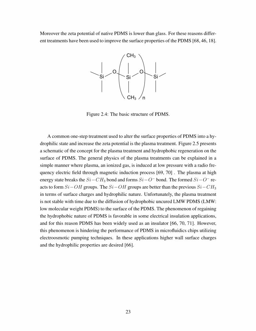
PMMA (polymethyl accurlate), SU-8 polyethylene, and PDMS (polydimethylsil-cone) [62, 63, 50, 64, 65], are polymeric based materials that have been used as channelsubstrates in microfluidics applications. One widely used polymeric material for mi-crochip fabrication is polydimethylsilcone (PDMS). PDMS is an amorphous hydropho-bic polymer [62, 63] where low molecular weight species diffuse inside the bulk material[66]. The surface has a negative surface charge when it comes into contact with a polarsolution. The chemical structure of PDMS is (C2H6OSi)n shown in figure 2.4. Com-mercially, PDMS is available in a viscous liquid form and cure after adding a curing-agent. PDMS properties, such as optically transparent, bio-compatible, and supportingelectroosmotic flow, suited different applications in microfluidics. In addition, PDMS hassome flexibility which has been utilized to make active valving and pumping elements[31, 67]. On the other hand, PDMS is not suitable for all microfluidic applications [68].Problems such as sample adsorption and non-compatibility with some chemical solventslimit its use in some biological sample analysis and chemical synthesis [68, 46, 18].
22
Moreover the zeta potential of native PDMS is lower than glass. For these reasons differ-ent treatments have been used to improve the surface properties of the PDMS [68, 46, 18].
O
Si
CH3
CH3
n
Si
O
Si
Figure 2.4: The basic structure of PDMS.
A common one-step treatment used to alter the surface properties of PDMS into a hy-drophilic state and increase the zeta potential is the plasma treatment. Figure 2.5 presentsa schematic of the concept for the plasma treatment and hydrophobic regeneration on thesurface of PDMS. The general physics of the plasma treatments can be explained in asimple manner where plasma, an ionized gas, is induced at low pressure with a radio fre-quency electric field through magnetic induction process [69, 70] . The plasma at highenergy state breaks the Si−CH3 bond and forms Si−O− bond. The formed Si−O− re-acts to form Si−OH groups. The Si−OH groups are better than the previous Si−CH3
in terms of surface charges and hydrophilic nature. Unfortunately, the plasma treatmentis not stable with time due to the diffusion of hydrophobic uncured LMW PDMS (LMW:low molecular weight PDMS) to the surface of the PDMS. The phenomenon of regainingthe hydrophobic nature of PDMS is favorable in some electrical insulation applications,and for this reason PDMS has been widely used as an insulator [66, 70, 71]. However,this phenomenon is hindering the performance of PDMS in microfluidics chips utilizingelectroosmotic pumping techniques. In these applications higher wall surface chargesand the hydrophilic properties are desired [66].
23
Si
CH3
Si
CH3
Si
CH3
Si
CH3
Si
CH3
Si
CH3
Si
Si
CH3
Si
CH3
Si
CH3
Si
CH3
Si
CH3
Si
CH3
Si
OH
Si
OH
Si
OH
Si
OH
Si
OH
O-
Si
O-
Si
O-
Si
O-
Si
O-
Si
O-
Si-OHSi-OH
Si-OH
Si-CH3
Si-CH3
O3
plasma
(a) (b)
(c) (d)
Figure 2.5: Plasma treatment and the hydrophobic regeneration of PDMS.
One approach used to preserve the hydrophilic state of the plasma treated PDMS isto store it in a hydrated environment with deionized water or other aqueous solutions[66, 70]. This is because the formed Si − OH groups prefer environments with higherdielectric constant (εwater ≈ 80, εwater ≈ 2.6, εwater ≈ 1) which will keep the Si −OH on the surface of the PDMS. This approach is impractical for long storage timeperiods and chip transportation. For this reason simple and reliable treatment protocolsare needed for preserving the artificial hydrophilic and surface charge properties of thePDMS.
2.4.1 PDMS Treatments
The area of treating PDMS attracted researchers from different disciplines, especiallyresearchers in chemistry. The main goal was to perform simple treatment protocolswhile maintaining the cost and time effectiveness of manufacturing PDMS based mi-crochips. There are several approaches to modify and improve the surface propertiesof the PDMS for microfluidics applications which has been examined in the literature[18, 72, 73, 74, 75, 76, 77, 78]. Chemical based surface treatments, such as prepolymeradditives, reducing the diffusion effects of the LMW PDMS, and grafting monomerswith the desired properties on the surface of the PDMS are commonly used. A review ofthe surface treatments for microfluidics applications is presented by Liu and Lee [79].
24
The addition of prepolymer additive to PDMS was investigated by Luo et al. [78].In their work acrylic acid (AA), and undecylenic acid (UDA) where separately mixedwith PDMS samples before the curing process. The additives were expected to merge inthe PDMS matrix without affecting curing process. In their treatment the PDMS chan-nels were naturally bonded to the substrate. The additives increased the electroosmoticmobility of the PDMS microchannels. Also, it was found that this approach affects thephysical properties of the PDMS. On the other hand, the treatment did not show an im-provement in the hydrophobic nature of the PDMS [78].
In order to improve the stability of the hydrophilic state for the plasma treated PDMS,researchers approached the problem from two main directions, which are: reduce orprevent the diffusion of the LMW to the surface of PDMS [71, 75], or create stablechemical groups with the desired properties on the surface of the PDMS [72, 73, 74, 76].
The reduction of the concentration of LMW in the PDMS prevents or at least reducesthe regaining of the hydrophobic groups on the surface of the plasma treated PDMS. Thereduction of the LMW concentration could be achieved by either thermal aging [75] orextraction of LMW PDMS [71]. In the thermal aging approach, the LMW concentrationis reduced due to the improvement in the cross linking of PDMS [75]. Eddington etal. [75] studied results of thermal aging on plasma treated PDMS samples with contactangle measurements. The work showed improvement and stability of the hydrophilicproperties of thermally aged PDMS. Also, it was found that the longer the aging pro-cess the better stability of hydrophilic properties for plasma treated PDMS. On the otherhand, thermal aging is a time consuming process and it is not desirable for fast chipmanufacturing.
The second approach for reducing the concentration of LMW is to perform chemicalextraction of the LMW from the cured PDMS [71]. This technique involves applicationof different chemical solvents to remove the non-cured LMW PDMS from PDMS bulkmaterial. Consequently, the stability of the plasma treated PDMS improves since theLMW concentration is reduced. Vickers et al. [71] performed a three stage extractionprocess to PDMS microchannels. It was found that the process reduces the weight ofthe PDMS by 5 %. This reduction is due to the removal of LMW from the PDMS. Theplasma treated and extracted PDMS showed stable hydrophilic properties compared tonative PDMS. The reason for this improvement in the stability is that the SiO2 com-pound was stable on the surface of the PDMS for long periods of time. The stability ofSiO2 was confirmed with X-ray photoelectron spectroscopy analysis. Moreover, the ex-traction process showed improvement in the electroosmotic mobility of the microchannelcompared to native PDMS [71].
25
Another approach that does not deal with changing the concentration of LMW inPDMS is to change the surface chemistry by grafting monomers that have the desiredchemical groups, such as −OH and −CN , on the surface of the PDMS [73, 74, 76, 79,80, 81, 82]. Different chemical compounds were used in the literature such as HEMA(2-hydroxy ethyl methacrylate) and acrylonitrile, Acrylic Acid (AA), PEG Poly(ethyleneglycol), which could be grafted on the surface of the PDMS [73, 74, 76, 79, 80, 81, 82].
He et al. [80] used an plasma induced grafting of acrylonitrile to form chemically sta-ble groups on the surface of PDMS. Results showed improved stability in the hydrophilicproperties of PDMS with dry storage conditions. Wang et al. [81] used APTES (amino-propyl triethylsilane) to treat the surface after plasma exposure and the results showedstable electroosmotic mobility with time. Hu et al. [76] used a UV approach to mod-ify the surface of the PDMS with different monomers, which were Acrylic Acid (AA),PEG Poly(ethylene glycol), and MATC (2-methacryloxy ethyltrimethylammonium chlo-ride) to improve the electrophoretic separation sample. Also, the electroosmotic mobilityproved to be stable with time compared to the non-grafted channels.
A chemical monomer that can be successfully polymerized on the surface of PDMSwith simple approaches is HEMA (Hydroxyethyl methacrylate). HEMA can be per-manently polymerized on the surface of PDMS by either plasma or a heat induced ap-proaches [73, 74, 82]. Bodas and Khan-Malek [73, 74] showed that HEMA could begrafted on the surface of the PDMS with the aid of oxygen plasma treatment. After theHEMA was grafted on the surface of PDMS, stable and hydrophilic chemical groups,Si − OH , were permanently formed. Their results were supported by both the contactangle and ATR-FTIR analysis. On the other hand, the plasma induced grafting approachhas some drawbacks and limitations to be facilitated in microchannel manufacturing.For instance, long plasma exposure time will cause mechanical aberration of the surfaceof the PDMS, which will create undesired surface roughness. Moreover it is hard touniformly spin coat HEMA on in the microchannels with precise thickness.
The other approach was to graft the HEMA with a heat induced approach [82]. Choiand Yang [82] used a heat induced approach to graft the HEMA on the surface of thePDMS. Figure 2.6 presents a schematic of the principle of the heat induced HEMAgrafting [82]. This is done by first forming active locations on the PDMS surface so thatHEMA will attach to it. The surface activation was achieved with the aid of air plasmatreatment. Afterwards, with the support of heat, HEMA will break the Si − OH bondand will be grafted to surface of the PDMS. Results of the heat induced HEMA graftingshowed the presence of stable OH groups with the ATR-FTIR analysis [82]. Moreover,improvement in the electroosmotic mobility of HEMA treated PDMS microchannels wasreported [82].
26
Figure 2.6: Basic concept of heat induced HEMA grafting [82].
2.4.2 Surface Characterization
The area of surface characterization of materials is a well established field [83, 84]. Inthe literature, different experimental characterization methods have been used analyzethe surface chemistry of PDMS specimens. Contact angle, XPS, and ATR-FTIR aresome examples for such techniques [71, 73, 75, 82]. In this work and for applicabilitypurposes two surface characterization methods are used to analyze the effects of thetreatments on the PDMS surface. The techniques are: the contact angle and ATR-FTIRanalysis. These techniques were chosen for valid reasons. Examining the nature of thehydrophilic properties of PDMS sample is done with contact angle measurements. TheATR-FTIR is used for finding the chemical changes on the surface of PDMS after thetreatments. A brief discussion on the theory of the contact angle and the ATR-FTIRanalysis is presented in Appendix A. For further information on the contact angle referto [1, 85]. Suggested readings about the ATR-FTIR analysis include [83, 84].
27
Chapter 3
Experimental Setup and ChannelManufacturing
Experimental studies, qualitative and quantitative, are powerful tools used to validatenew theories, examine certain phenomena, or perform parametric studies. In this workdifferent experimental techniques were adapted to perform parametric studies related tomicrofluidics applications. Figure 3.1 presents a flow chart that summarizes the processesof the performed studies and the integration process between them.
Chemicals used in this work can be divided into different categories according to theirfunction. Figure 3.1 presents the process of using the chemicals for different applicationsand their integration in the overall study.
The sample manufacturing is briefly discussed in this chapter. The samples are sortedinto: profiled and non-profiled samples. The profiled samples are used to manufacturethe samples in channel format and are studied with the current-monitoring technique(chapters ) and the dry storage analysis. The non-profiled samples are used in the contactangle and ATR-FTIR analysis (chapter 6).
The experimental setups used in this work are briefly discussed. The methodology forusing the current-monitoring system is postponed to chapter 4 since it is directly relatedto the goals of the chapter. The measurement for the contact angle and the ATR-FTIRare discussed in this chapter.
28
Figure 3.1: Flow chart of the experimental studies.
29
3.1 Chemicals and Reagents
The chemicals used in this work can be organized into four main categories: samplemanufacturing, solutions used in the surface treatment of PDMS, electrode calibrationbuffers, and solutions that were tested with the current-monitoring technique. Informa-tion about the different categories of chemicals are discussed next.
3.1.1 Chemicals used for Manufacturing the Microchannels
Samples in microchannel format were used in the current-monitoring studies (chapters4 and 5), dry storage analysis (chapter 6), and for examining the effects of chemicalsurface treatments on the PDMS (chapter 6). The studied microchannels were PDMSbased, since they are suitable to numerous microfluidic applications. The manufacturingof the microchannels and samples was done with a soft lithography and replica moldingof PDMS [62, 63]. The chemicals used in the manufacturing processes are listed below:
• SU8 (MicroChem Corp.): a polymeric resin used for creating solid profiles of themicrochannels on silicon or glass substrates. SU8 is a photoresist that crosslinkswhen exposed to UV light. The photoresist comes in different grades that corre-spond to the viscosity of the photoresist, which was correlated to the maximumheight of the SU8 hardened profiles [86].
• SU8 developer (Microchem Corp.): used to remove the uncrosslinked SU8 afterthe UV exposure and postexposure bake [86].
• TCMS (Trimethlylchlorosilane): is a toxic solution used to coat the hardened SU8profiles before the replica molding of the PDMS elastomer.
• PDMS Base (polydiemthylsilicone) Sylgard 184 silicone elastomer base (DowCorning, San Diego, CA).
3.1.2 Chemicals used for the PDMS Surface Treatment
The main goals of the attempted chemical treatments are to improve the hydrophilicproperties and enhance the zeta potential of PDMS based microchannels. In this work
30
three main chemically based treatments were chosen for applicability and their reportedresults. The treatments were: prepolymer additive, extraction of PDMS, and HEMAgrafting. The following chemicals were used:
• Acrylic acid (Fisher Scientific) was used in the prepolymer additive scheme.
• Triethylamine (Fisher Scientific) used in the PDMS extraction approach.
• Ethyl acetate (Fisher Scientific) used in the PDMS extraction approach.
• Acetone used in the extraction approach scheme.
• HEMA (2-hydroxyethyl methacrylate) (Sigma Aldrich) was used in the monomergrafting methods.
3.1.3 Calibration Solutions
The precise measurement of the solutions pH and conductivity is important for the accu-rate interpretation of the current-monitoring outcomes. High accuracy electrodes wereused for measuring the solution properties. For the purpose of calibrating the pH andconductivity electrodes three conductivity buffers were purchased from VWR for eachelectrode. The conductivity buffers were of values 100 µS/cm, 1400 µS/cm, and 10,000µS/cm, which cover the conductivity range of solutions used. The pH calibration bufferswere pH 4, pH 7, and pH 10.
3.1.4 Solutions Tested with the Current-Monitoring Technique
One of the goals of this work was to estimate the electrostatic properties of biologicalbuffers that have not been reported in the literature. Some of the buffers are known asGood’s buffers, in reference to criteria proposed by Good et al. [87]. Other buffersare commonly used in the biological analysis community for DNA, RNA and proteinanalysis. The solutions were:
• 1X TAE-pH 8.08 (40 mM Tris base, 20 mM Acetic acid, and 1mM EDTA).
• 1X TBE-pH 8.24 (89 mM Tris, 89 mM boric acid, and 2 mM EDTA ).
Some buffers came as batches of the high concentrated solutions, such as 10X MOPSand10X PBS. The high concentrated buffers were diluted from the concentration of 10Xto 1X with ultrapure1 water (1 to 9 ratio, buffer to water). Other buffers were preparedin the lab such as 1X TBE and HEPES. The pH of the buffers was measured during thesolution preparation with the pH electrode, and if needed, titration was performed. Allsolutions were filtered through a 0.2 µm filter before using them in the actual current-monitoring experiments.
3.2 Sample Manufacturing
In this work, only PDMS based microchannels were studied because of there vast appli-cability in microfluidics [62, 63]. The manufacturing technique is known as soft lithog-raphy technique. The process goes through two main steps:
• First manufacture the appropriate masters that has the channel profiles.
• Second, replica mold of the microchannels and non-profiled samples with PDMSelastomer [62, 63].
A simple description of the procedure for manufacturing the channels masters is pre-sented in Appendix B Section B.2.
The samples are into two main formats: microchannel and non-profiled formats. Themicrochannel formats are used in the: current-monitoring studies (chapters 4, 5), the dry
1Ultrapure water is a commonly used term for high filtered de-ionized water. The extra filtering stepremoves impurities and particles from the water. Also, it the total organic carbon and the water electricalconductivity are controlled. The electrical conductivity of ultrapure is less than 10 µS/m
32
storage analysis (chapter 6), and the PDMS chemical surface treatment studies (chap-ter 6). The non-profiled PDMS samples are used in the contact angle and ATR-FTIRanalysis (chapter 6).
Air plasma treatment is used to alter the surface properties of PDMS and help thebond the channel to the substrate. The system used is the PDC-001 plasma-cleaner (Har-rick Plasma, Ithaca, NY). The common plasma treatment protocol is 29.6 W for 40 s,unless otherwise specified. Figure 3.2 shows a photograph of the plasma treatment sys-tem and a typical PDMS chip.
PDMS and substrate
Substrate
Reservoirs
Figure 3.2: Plasma treatment system and a typical bonded chip.
3.3 Experimental Setups
In this work the different experimental setups were used to perform numerous studies.The following systems were used: solution property measurement devises, the current-monitoring setup, the ATR-FTIR system, contact angle system, and the fluorescencemicroscopy system. Information about each of these systems will be provided next.
3.3.1 Solution Property Measurement
The three important solution properties that have a direct effect on the electroosmoticflow in microchannels are the temperature, the solution pH, and the conductivity. Con-ventional electrodes can not be used for measuring the solution properties in the chipdue to the space and volume limitations at the reservoirs. Hence, small electrodes withhigh accuracy were needed. The temperature was measured with a high accuracy K-type (chromel-alumel) thermocouple. The pH and conductivity were measured with the
33
MI-915 and MI-4154 electrodes (Microelectrodes Inc Bedford, USA). The electrodeswere connected to an Orion 5 Star meter (Thermo Electron Corporation) for outputtingthe readings. The electrodes were frequently calibrated prior current-monitoring exper-iments, each with appropriate buffers. A three point calibration procedure was done forthe each electrode. After the calibration the conductivity electrode was kept in a bottlewith ultra pure water, while the pH electrode was preserved in an active buffer of pH7.
3.3.2 Current-Monitoring System
The basic concept of the current-monitoring technique is to record the electrical currentwhile performing electroosmotic pumping in microchannels. Thus, an electrical voltagesupply and a current measurement system are needed. A schematic of the connectionsbetween the components of the current-monitoring system is presented in figure 3.3. Themain components of the current-monitoring system used in this work and the operationof each element are listed as follows:
• DC power supply (Spellman SL10*10 B.3.1).
• Current measurement system.
• Electrical switch.
• Chip holder.
• Data recording and monitoring system.
• AC - Fan.
34
Electrical
Switch
Ground
R Waste
Computer
Air @ room Temp
Fan
Lside
+V L d
+ -
R1
R2
Pico-Ammeter
Keithley
Power supply
Spellman
DAQPC
Figure 3.3: Schematic of the current-monitoring experimental setup.
.
The electrical switch and the chip holder were in-house assembled components asshown in figure 3.4. The main function of the AC fan was to keep the chip assembly atroom temperature during experiments. The electrical current measurement system willbe discussed next. For more information about the current-monitoring main componentsand specifications refer to Appendix B, Section B.3
In the first stage of current-monitoring experiments the current recorded from theSpellman was sufficient for measuring electrical currents above 2 µA with an acceptedaccuracy in distinguishing important points of the current-time plot. However, the elec-trical current exported from the Spellman showed severe noise. In addition, preliminaryresults of the surface conductance during electroosmotic flow were negative, which con-tradicts with the physics of the electroosmotic flow. For this reason a high accuracyPico-Ammeter (Keithley 6485) was integrated in the current-monitoring system. Thiswas done to assure accurate electrical current measurement. Figure 3.4 presents a typicalcurrent-time plot recorded during an actual current-monitoring experiment with both theSpellman power supply and the Keithley pico-ammeter.
35
(a)
(b)
Figure 3.4: Electrical current comparison. (a) Keithley Pico-Ammeter, and (b) Spellmanpower supply.
.
As shown in figure 3.4, it is apparent that both current-time plots from the Spellmanpower supply and the Pico-Ammeter were giving close trends in distinguishing importantpoints of current changes. On the other hand, the Spellman is underestimating the actualcurrent by about 3 % compared to the Pico-Ammeter. Moreover, the signal from theSpellman is noisy. Given that the accuracy of the electrical current measurement fromthe pico-ammeter is higher than the accuracy of measuring the current from the Spellman,it is believed that the current recorded from the pico-ammeter is closer to the real timeelectrical current during electroosmotic pumping. This supports using the Pico-Ammeterin the current-monitoring experiments.
Note: to integrate the Pico-Ammeter to the current-monitoring setup a surge protec-tion circuit must be used. Refer to Keithley Low Level Measurements Handbook [88].
3.3.3 ATR-FTIR System
The ATR-FTIR analysis is a non intrusive technique used to find the presence of differentchemical groups in samples [83]. The ATR-FTIR analysis was adapted to study thechemical groups present in the PDMS samples since the samples were around 2 mmthick. The ATR was also used to examine the chemical surface treatments for the PDMS,as will be presented in chapter 6.
36
In the present study the TENSOR 27 (Bruker Optics Ltd., Milton, ON, Canada) isused to analyze the treated and non-treated PDMS samples. The TENSOR 27 is capa-ble of finding the IR spectrum ranging from 400-4000 cm−1. To obtain the infra redreflectance signal an ATR MVP-SplitPea accessory with a hemispherical shaped siliconcrystal (Harrick Scientific Inc, Pleasantville, NY) was used. The crystal has a refrac-tive index of 3.4. For an organic sample with a refractive index of 1.5 the penetrationdepth of the IR signal is 0.41 µm at a wave number of 2000 cm−1. The control of theTENSOR 27 ATR-FTIR system was achieved with OPUS program (Bruker Optics Ltd.,Milton,ON) which was the interface between the TENSOR 27 and the PC. Figure 3.5presets the system used for the ATR-FTIR analysis.
The size of the PDMS samples that were tested with the ATR-FTIR system are 3cm × 3 cm in order to provide adequate clamping on the silicon crystal. At least threesamples for each treatment were prepared for ATR analysis. For each sample, at leastthree locations are measured. Each measurement covered the range 400 - 4000 cm−1
with a 4 cm−1 step, and 32 scans were obtained in a single measurement. The measure-ment startes by obtaining the background spectra for the surroundings. Then the PDMSsample is clamped over the silicon crystal with a torque of 8 cN ·m, and the measure-ment is performed. After each measurement the silicon crystal is wiped with acetone forcleaning purposes. The results of the ATR-FTIR analysis will be disscussed in chapter 6.
Silicon
Crystal
Figure 3.5: Bruker (TENSOR 27) FTIR system. Enlarged figure is the ATR MVP-SplitPea accessory.
37
3.3.4 Contact Angle System
Contact angle measurement of small solution droplets on solid surfaces gives importantinformation about the nature of the surface. The contact angle measurement was chosento examine the surface properties of the PDMS used in the channel and sample manufac-turing before and after different treatments. The studies covered the effects of the plasmatreatment on PDMS. Also, the chemical treatment effects on the properties of PDMSwere examined, as will be discussed in chapter 6.
The contact angle measurements are performed with a prearranged system on a vibra-tion free table. The system includes a CCD camera (CHOU model 4915-20001) whichwas connected to an acquisition and analysis system. PDMS samples with size 1.5 cm× 1.5 cm were used in the contact angle measurements. The sample was positioned ona sample holder in front of the camera optics. Ultrapure water droplet was put on thesample and the monitoring system was used to assure that the droplet is symmetric. Aseries of images was taken with the camera. In a typical measurement 30 images wererecorded for a one point. The final result was the average of the 30 images. Moreover,for each sample at least two points of contact angle measurements were performed. Theprogram used to analyze the images was ADSA (Axisymmetric drop-shape analyses)software. Figure 3.6 presents a photographic image of the system used for the contactangle measurements.
CCD camera
(CHOU
4915-2001)
Monitoring
system
Acquisition
and analysis
system
Figure 3.6: Contact angle measurement system.
38
3.3.5 Fluorescence Microscopy System
A fluorescence microscopy system was used for different applications and sample imag-ing. An inverted microscope (GX71, Olympus) with numerous dry objectives was usedin various studies. The main properties of the objectives are listed in table 3.1.
Table 3.1: Microscope objectives specifications.
Working NumericalObjective name Magnification distance Aperture
The choice of the microscope objective depends on the size of the area of interest inthe sample. If the area of interest is small high magnification objectives were used, andvise versa. Figure 3.7 presents a schematic of the sample view and the observed area ofinterest from the microscope objective. Light illumination was performed with a halogenlamp mounted on the back of the microscope. The microscope was also equipped withan Olympus filter cube (BSWM) for the purpose of fluorescence imaging. This filter isideal for the imaging the commonly used fluorescent dye (Invitrogen Corp).
39
Front
Section of
the channel
Top section of
the channel
Microscope
objective
Microchannel
Area of interest viewed
from the microscope
objective
Channel
Walls
Channel
Wallsw
h
Front section
Top section and field of
view from the objective
Micorchannel
Microscope objective
Figure 3.7: Schematic of the area of interest in microchannel observed from the micro-scope objective.
The imaging of the viewed samples was performed with a CoolSNAP ES CCD cam-era (1392x1040 pixels, Photometrics) which was coupled to the microscope system. Theimage capturing and analysis was carried out with the Image-pro Plus software (MediaCybernetics). Figure 3.8 presents a photographic image of the microscopy system.
The microscope was frequently used for the verification of both the master and thechip that will be tested in the current-monitoring experiments to assure the absence ofdefects. Also the system has been used for flow visualization of electroosmotic pumpingin the Y-channel design as will be presented in chapter 4.
40
CCD Camera
CoolSNAP ES
Inverted microscope
Olympus GX-71
Image acquisition
and analysis
Sample location
Figure 3.8: Fluorescence microscopy system.
3.4 Final Remarks
In this chapter general information about the chemical used, sample manufacturing pro-cess, and experimental setups were presented. A descriptive overview of the microchan-nel manufacturing process is discussed in Appendix B.2. The processes of chemicallytreating the PDMS samples will be presented in chapter 6, since it is directly related tothe goals of the chapter.
The experimental setups were generally overviewed. The procedures in perform-ing the measurements with each experimental system will be presented in the relatedchapters. Studies with the current-monitoring system will be discussed in chapters 4and 5. The ATR-FTIR and contact angle systems were used in the characterization ofthe chemical treatments, as will be presented in chapter 6. An overview of the uncer-tainty parameters of the current-monitoring system is presented in Appendix C. Also, anoverview of the error propagation is discussed in Appendix C.
41
Chapter 4
A New Channel Design for theCurrent-Monitoring Technique
In this chapter a new Y-channel design1 will be presented, analyzed and validated forstudying the electrostatic properties of the microchannel along with the current-monitoringtechnique. Errors from the undesired pressure driven flow and electrolysis were ad-dressed and reduced in the new channel design.
4.1 Introduction
Electroosmotic flow utilizes the presence of the EDL to create a flow within microchan-nels. By applying an electric field tangentially to the EDL the mobile ions in the EDL willmove to an appropriate electrode, and with viscous effects the moving ions with in theEDL will drag the solution in the region out of the EDL [4, 11, 26]. Figure 4.1 presents aschematic of an electroosmotic flow with the driving body force inside a microchannel.As discussed in chapter 2, for a thin EDL compared to the channel characteristic lengththe average velocity in the microchannel is approximated with the slip velocity, which isfound from the Helmholtz-Smoluchowski equation 4.1:
uslip = −εo · εr · Eµ
· ζ = µemo · E (4.1)
where uslip is the slip velocity at the shear layer of the EDL, E is the electrical field, εr
the solution relative permittivity, εo the vacuum permittivity, ζ is the zeta potential, and
1The introduction of the Y-channel design was done in the IMECE2007 conference, in Seattle 2007[89]. The first paper discussing the Y-channel is published in the proceedings of the conference [89].
42
µ is the viscosity of the solution. Another commonly used term is the electroosmoticmobility µemo of the microchannel which groups the solution properties with the zetapotential into one value.
- - - - - - - - - - - - -
- - - - - - - - - - - - -
+ ive- ive
uemo
Shear plane
- ive surface charge
x
y
Microchannel wall
++ ++ ++ ++ ++ ++ ++
++ ++ ++ ++ ++ ++ +
Ex
)(Voltφ
- -- - - - - - - -
+
Ψ(y) (Volt)
ζ
- - -- - -+ + + + + + + + + + + +
+ +
++
+
+
+
+
+
+
++
+
+
+
+
++
+
+
+
++
+
++
+
+
+
+
+
+
++
+
+ + + ++
++
+++
Ψs
++uslip
yShear plane
- -x
y
Ex
Diffuse layer
Figure 4.1: Schematic of electroosmotic flow in a microchannel.
Electroosmotic flow has been widely used in several microfluidic applications be-cause the ease of implementation in the microchips, fast response time, ease of controlthrough complex channel geometry, and most important is the plug like velocity profile[4, 11, 51]. The significance of the plug like profile comes from that it does not allowsample dispersion, thus increasing the accuracy of analyte detection. The most impor-tant factor that defines the electroosmotic flow in microchannels is the zeta potential.This property is unique for each solution wall pairing, thus it is important to accuratelymeasure its value.
The current-monitoring technique is the most widely adopted method for finding thezeta potential of microchannels due to its simplicity of the hardware, ease of interruptingthe results and accuracy [4, 46, 41, 42, 47, 48, 49, 50, 51, 52]. In this method the averageelectroosmotic velocity is measured by qualitatively monitoring the current change as thetest solution is replaced by the same solution but with a slightly different concentration(i.e. lower conductivity) in a straight microchannel. It is important that the concentrationdifference be small (≈5% concentration difference) or inaccuracies will occur due tovariations in zeta potential between the two solutions. By knowing the time needed for
43
solution replacement in the microchannel and the channel length the solution averagevelocity inside the microchannels could be estimated:
uav =L
M t(4.2)
where L is the channel length where the solution is being replaced, and M t is the timeneeded for the full solution replacement within the microchannel (ie. from one reservoirto the second reservoir). The full replacement is identified by reaching a steady electricalcurrent value, which indicates that only a specific solution is pumped in the microchan-nel. Afterwards the zeta potential is inferred from the Helmholtz-Smoluchowski slipvelocity 4.1 for a thin EDL compared to the channel characteristic length. A simpleschematic of the principle of the current-monitoring technique with a typical current-time plot reported from the literature is presented in figure 4.2.
Ren et al. (2002)
(b)
Figure 4.2: Schematic of the principle for the current-monitoring technique and a typicaloutcome [19, 48].
As discussed in chapter 2, previous current-monitoring experiments did not addressseveral problems that have an affect on the current-monitoring results. Issues such as un-desired pressure driven flow and electrolysis were not discussed nor were the prevented.Also, other problems were encountered when using the current-monitoring techniquewith microchannels in chip format, such manual removal of the solution at the reser-voirs and positioning the electrodes. The nature of the technique requires continuousinteraction with the hardware and experimental setup. The solution removal at the reser-voirs was done manually with no assurance of emptying the reservoirs. Moreover, thecurrent-monitoring experiment must be repeated several times to obtain consistent results
44
for identical experimental conditions. This process was time consuming and the resultswere not reliable.
In this work a Y-channel design was presented to study the electrostatic properties ofPDMS based microchannels with the current-monitoring technique. The main aspects ofthe design will be discussed in the next sections.
4.2 Y-Channel Design
In the Y-channel design, two side channels are connected to a displacement channel, asschematically shown in figure 4.3. The basic concept of the design is to fill the two sourcereservoirs, R1 and R2, with the high and low concentration solutions, 100% and 95 %concentrations. The solution pumping is alternated between the two source reservoirs.This is achieved with an electrical switch that is connected to the electrodes touching thesolutions at the source reservoirs. The current is monitored while the pumping process isperformed from the reservoirs and replacement is occurring in the displacement channel.This design offers the ease of repeating the experiments several times by only changingthe direction of the applied electric field, thus; performing more measurements withoutthe need of manually removing the solutions from the reservoirs.
R surface
R fluid
R surface
L side
Ld
+V
-V
Floating
-V
E (V/m), Q (m3/s)
+V
Electrical
switch
I (A)
R fluid
R1
R2
R3
Figure 4.3: Schematic of the proposed Y-channel design.
The operation principle of the Y-channel design is as follows. First an electric fieldis applied between the high concentration (R1) solution and the third reservoir ( R1 →R3 ), while leaving R2 floating, which will pump the high concentration solution in thedisplacement channel. The electrical current is monitored during the process and full
45
solution replacement inside the displacement channel is indicated by reaching a steadycurrent value. Afterwards, the electric field direction is applied to the other reservoirwith the electrical switch, and the electric field is applied from R2 to R3 while leav-ing R1 floating. The low concentration solution is pumped inside the displacement (Ld)microchannel, casing a change in the current due to difference in the solution conduc-tivity. The current is monitored while the low conductivity solution was being replacedinside the displacement microchannel. Likewise, full replacement was indicated whenthe current reach a plateau.
Figure 4.4 presents the expected current-time plot from the Y-channel design duringthe two pumping scenarios, and the current-time plot for a straight channel design withthe same geometrical aspects ( same cross-section area and Lchannel = Ld + Lside).
Time (s)
Cu
rren
t (
A)
t1 t2
I1
I2
∆t ∆t
Slope
Straight
channel E
E
+V
+V
-V
Ld
Lside -V
Figure 4.4: Expected current trend during the replacement from the Y-channel design.The red line represents pumping the low concentration solution (R2→ R3), the blue linerepresents pumping the high concentration solution (R1 → R3), and the dashed line isthe expected current from the straight channel design.
Notice, in both cases, the slope of the current-time relationship is the same. Thecurrent-time trend from the Y-channel design is similar to a straight channel design par-tially filled with the solution being replaced. The average velocity of the solution duringthe replacement in the Y-channel design can be calculated as:
uav =Ld
M t(4.3)
where Ld is the length of the displacement channel and M t is the time needed for the fullreplacement of the solution inside the channel. By comparing the current draw from the
46
Y-channel to the straight channel designs there are some noticeable differences. In theY-channel and immediately after switching there is a sudden change in the current, eitherdrop or increase. This is due to the fact that the side channel is already filled with thesolution that has a different conductivity from the solution which is in the displacementchannel at the time of the switch. The magnitude of the sudden current change is in-fluenced by the solution electrical resistance from the side channel to the total electricalresistance between the reservoirs. If the cross-sectional area of the side channel is sim-ilar to the displacement channel, which is the case in these designs, the relation reducesto be a geometrical ratio of side channel length to total length between the reservoirs(Lside/Lchannel, where Lchannel = Ld + Lside).
4.2.1 Undesired Pressure Driven Flow
In devices utilizing electroosmotic flow, undesired pressure driven flow limits the through-put and stability of the device operations conditions [16, 61]. In the presence of bothpressure driven and electroosmotic flows the velocity in the microchannel will be thesuperposition of the two components.
The accuracy of the current-monitoring technique in finding the zeta potential ofmicrochannel is affected by the pressure driven flow since it finds the average velocity ofthe of the pumping without distinguishing the either velocity component. However, if thepressure driven flow can not be eliminated and its magnitude and direction are known,the electroosmotic velocity could be found by accounting for the average velocity of thepressure driven flow.
There are two main contributors for the pressure driven flow in current-monitoringtechnique for channels that must be addressed: solution height differences between thereservoirs and Laplace (meniscus shape differences) pressure effects. In order to performaccurate current-monitoring measurements pressure driven flow must be eliminated.
An effective approach for reducing the effects of the undesired pressure driven flowis to increase the hydrodynamic resistance of the microchannel. The hydrodynamic re-sistance for a microchannel can be approximated by equation 4.4:
Rhyd =12 · µw · h3
(4.4)
where L is the channel length, µ is the solution viscosity, w is the channel width, and his the channel height. In order to effectively increase the hydrodynamic resistance thedenominator must be reduced. This could be done by either decreasing the channel widthor height. Changing the channel height is more effective since its effect is powered by
47
three (Rhyd ∝ 1/h3). On the other hand the channel height must not be in the sameorder as the scale of the EDL thickness so that the approximation of the Helmholtz-Smoluchowski equation 4.1 is still valid.
As presented in chapter 2, the thickness of the EDL is in the same order of the Debyelength scale. And it is known that for very dilute solutions the thickness of the EDL isvery high. i.e. for ultra pure water the thickness of the EDL is around 300 nm [11].Hence, the characteristic length of the channel dimensions must not interfere with thethickness of the EDL, in order for the approximation of equation 4.4 to be valid.
Figure 4.5 presents the effect of changing the channel height on the velocity ratioof pressure driven flow to electroosmotic flow, (upressure/uelectroosmotic), in a situationwhere the pressure difference between the reservoirs is around 100 Pa and the solutionhas a very low electroosmotic velocity, 166 µm/s2.
0.00
5.00
10.00
15.00
20.00
25.00
30.00
35.00
40.00
45.00
0.00 5.00 10.00 15.00 20.00 25.00
% u
pre
ssu
re/ u
ele
ctr
oo
sm
oti
c
Channel height (µm)
Figure 4.5: Channel height affect on the velocity ratio (upressure/uelectroosmotic). Theanalysis was performed for a pressure difference of 100 Pa between the reservoirs and anaverage electroosmotic velocity of 166 µm/s .
The analysis presented in figure 4.5 was performed to prove the concept of the effectof changing the channel height height on the velocity ratio (upressure/uelectroosmotic). The
2This average velocity is equivalent to pumping a solution with very low electroosmotic velocity, suchas 1X PBS buffer. The example presented in figure 4.5 is performed for an applied electric field of Ex =10kV/m and a solution having an electroosmotic mobility of µemo = 1.66× 10⁻⁸m2/V · s.
48
values of the electroosmotic velocity and the induced pressure difference between thereservoirs were chosen to be severe situations. In most cases the electroosmotic velocityin microchannels is higher than 166 µm/s. Also, this pressure difference was equivalentto solution height differences of 1 cm between the reservoirs, which was not allowed inthe real experimental conditions.
As shown in figure 4.5, the velocity ratio is below 10 % when the channel height is be-tween 5 - 10 µm. Thus, the error from the undesired pressure driven flow is significantlyreduced and it is within the uncertainty of the measurements from a typical experimentalsetup, as presented in Appendix C. Moreover, this range of channel heights does not vi-olate the approximation of the average velocity with Helmholtz-Smoluchowski equation.
4.2.2 Solution Electrolysis Effects
Electrolysis of the background electrolyte, at reservoirs, has severe effects on applica-tions where the solutions must maintain a certain pH value, such as DNA electrophore-ses. Thus, it must be eliminated or significantly reduced. This motivated researchers inthe chemistry discipline to study solution electrolysis experimentally and numerically inorder to overcome these problems [40, 41, 90, 91].
The major problems associated with electrolysis in electroosmotic pumping are asfollows:
• Changing the solution properties [40, 41, 90, 91].
• Creating bubbles around the electrodes that are used to implement the electricfields 3.
• Depleting the solutions at the reservoirs [19].
One important issue with electrolysis that affects the stability of electroosmotic pump-ing is the formation of bubbles around the electrodes. The formed bubbles increases theelectrical resistance during electroosmotic pumping since they will form an insulatinglayer around the electrode. These bubbles create an unsteady electroosmotic pumpingconditions. This trend has been observed in preliminary current-monitoring experimentswith the Y-channel design for 10 and 9.5 mM KCl. Figure 4.6 shows the effect of bubblesformation on the current-time plot during long term electroosmotic pumping.
3This was observed in preliminary current-monitoring experiments performed in the lab.
49
(a)
(b)
(c) (d)
Figure 4.6: current-monitoring experiment for 10 mM KCl and 9.5 mM KCl. The experi-ment was performed for four different applied voltage differences between the reservoirs,(a)-250 V, (b)-500 V, (c)- 750, and (d)- 1000 Volts during which the solutions were keptin the reservoirs.
From the current-plot shown in figure 4.6, there is a clear and repeatable trend forthe solution replacements in regions (a), (b), and (c). In these regions, the replacementbetween the 9.5 mM KCl and 10 mM KCl was occurring and clearly identified. On theother hand, the forth region (d) there was neither a clear trend nor stable solution re-placement as indicated in the current-time plot. Bubbles were observed on the electrodesduring this experiment, which affected the stable pumping conditions of the solutionssince the applied electric field was fluctuating due to the change of electrical resistance.Also, the solution pH changed at the source reservoirs from 6.83 to 3.5 during the ex-periment. Fluctuations in the recorded current were attributed to the forming of bubblesaround the electrodes and to the unstable changes of the solution pH at the reservoirs.
Another problem that electrolysis has on the current-monitoring technique is its ef-fects in changing the solution conductivity. This is due to the formation of free ions dur-ing electrolysis that contributes to an increase in the local solution conductivity whichis being pumped in the microchannel. In the current-monitoring experiment this unpre-dictable change in current creates a chance of not accurately finding the end of solution
50
replacement during the electroosmotic pumping. This problem has severe effects on so-lutions that have low or no buffering capabilities, such as electrolytes and buffers withhigh electrical conductivity. Figure 4.7 presents the electrolysis effects in changing thesolution conductivity during a current-monitoring experiment for 1XPBS buffer.
End of
replacement
Figure 4.7: current-monitoring experiment for 1X PBS.
In this experiment the channel was filled with 1X PBS, the 100 % solution, and itwas replaced with 95 % 1X PBS solution, as it is clear from 4.7. After the replacementhas ended there was an increase in the recorded current. To have a better understandingon the nature of solution property changes during this experiment, table 4.1 presents pHand conductivity properties before and after the experiment.
51
Table 4.1: Solution property change during current-monitoring experiment presented infigure 4.7 with 1X PBS.
pH Conductivity λb
(µS/cm)
pH1 pH2 λb1 λb2 %4λb
Reservoir 16.7 6.62 11,260 11,490 2.04%
1XPBS (100 %)Reservoir 2
6.67 6.60 10,830 11,100 2.49 %1XPBS (95 %)
Reservoir 36.67 6.99 11,180 11,820 5.72 %
1XPBS (100 %)
As observed in table 4.1, the solution property changes during this experiment arecaused by electrolysis since the temperature at the reservoirs did not change. In thisexperiment the electric field was applied to the solutions in the reservoirs for 14 minutes,which increased the undesired electrolysis effects. This trend, showing the effect of pHchanges on conductivity, was also observed by Rodriguez and Chandrasekhar [41]. Thus,to perform accurate current-monitoring experiments, certain precautions and remediesmust be done to reduce the effects of electrolysis.
As seen previously, electrolysis as a phenomenon associated with electroosmoticpumping could not be eliminated. Hence, it is the toughest obstacle confronting elec-troosmotic pumping in microchips. Reducing the effects of electrolysis is importantfor the long run of electroosmotic pumps. Also, for accurate interpretation of current-monitoring experimental outcomes, electrolysis must be significantly reduced.
Figure 4.8 presents a schematic of the different phenomena occurring during solutionelectrolysis that have an effect on the current-monitoring technique.
52
E (V/m), u (m/s)
+V -V
E (V/m)
+V -V
(A)
(B)
Pt Electrode
Microchannel wall
Reservoir
Figure 4.8: The electrolysis phenomena and its effects on the solutions at the reservoirsduring electroosmotic pumping. White dots represent the bubble formation around theelectrode and red regions represent electrolyzed solution parcels. (a) First Y-channeldesign and (b) final Y-channel design.
As shown in figure 4.8, the two major phenomena associated with electrolysis thathave an affect on the current-monitoring technique are the bubble formation at the elec-trodes and the diffusion of the parcels of electrolyzed solution in the channel. Thesetwo phenomena could be significantly reduced by using large volumes of solution at thereservoirs which will absorb small electrolysis changes around the electrodes. Anotherremedy was to position the electrodes far away from the entrance of the channel. Thiswill allow more time for performing the experiment before parcels of electrolyzed so-lution enters the microchannel. Macka et al. [40] found that to reduce the effects ofelectrolysis in capillary electrophoresis application the electrodes should be positioned1 mm above and 1 mm away from the capillary entrance [40]. This will give more timebefore the electrolyzed solution reaches the microchannel.
In the present work large extended reservoirs, as shown in figure 4.8, were used forthe current-monitoring experiments. The electrodes were positioned 1.5 cm above theentrance of the channel.
Another important safety measure that has an influence in reducing and delayingelectrolysis was to reduce the current draw during electroosmotic pumping. This wasdone by increasing the electrical resistance of the channel/solution configuration. In a
53
microchannel, the electrical resistance of the solution is found from equation 4.5:
Relectrical =L
λb · Ac
(4.5)
where L is the channel length, λb is the solution bulk conductivity, and Ac is the crosssectional area of the microchannel. By using a shallow channel the cross section areawill be reduced. This will reduce the effects of electrolysis, as it will also reduce theundesired pressure effects, as disused in the previous section.
Nevertheless, to insure that the electrolysis effects were reduced in the current-monitoringtechnique several precautions were taken during the current-monitoring experiments:performing the experiment at low currents, shortening experiment times for non-bufferedsolutions, replacing the solutions after each stage of the experiments if needed, and theplatinum electrodes were touching the tip of the solutions in the reservoirs.
4.3 Experimental Setup and Procedure
The main Y-channel design aspects and the experimental procedure will be presentednext.
4.3.1 Y-Channel Designs Aspects
Based on the forgoing discussions, the major aspects of the Y-channel design were de-cided. First, the side channel to the displacement channel lengths was chosen to be 1:4.This ratio will provide more time for the solution to be displaced in the microchannel,which makes it easer to locate the start and end of the solution replacement. Channelheights were chosen to be in the range of 5 - 10 µm, which will significantly reduce theeffects of undesired pressure driven flow and electrolysis. To assimilate the variety ofsolutions that will be studied numerous masters with different dimensions of Y-channeldesigns were manufactured in the same approach presented in chapter 3. A summary ofthe Y-channel designs is presented in table 4.2:
54
Table 4.2: Dimensions of the fabricated masters for the Y- channel designs.
An appropriate Y-channel design is chosen for the solution that will be studied in thecurrent-monitoring experiment. This is done by finding the expected channel cross sec-tional area from equation 4.6, and under an applied voltage 750 V and a current 2 - 10µA, and using the equation:
Ac exp =I · Lchannel
V · λb
(4.6)
whereAc exp is the channel cross-sectional area of the channel, Lchannel is the total lengthof the channel, I is the current, V is the voltage, and λb is the solution conductivity.The current was chosen in this range because of the accuracy of current measurementsystem. The electrical current renge condition (2 - 10 µA) was applied when recordingthe electrical current from the Spellman power supply. However, if the Pico-Ammeterwas used the electrical currents could be recorded with smaller values, refer to figure 3.4.
Prior to performing the current-monitoring experiment a branch symmetry validationwas done for each Y-channel chip. The validation was a two step procedure. First a checkwith the microscope was done to assure that there were no obvious dimensional defectsin the channels. The second step of the symmetry validation was done by filling bothreservoirs R1 and R2 with the same solution and alternate the pumping source betweenthe reservoirs with the same applied electrical field while monitoring the current for eachpumping scenario. If both branches were symmetrical the current draw during pumpingwill be identical regardless of the source reservoir. After the symmetrical validation wasconfirmed, new solutions were introduced into the reservoirs. The first reservoir containsa 100 % solution, while R2 contains the same solution but diluted to 95 %. The solution
55
properties such as the temperature, pH and conductivity were measured at the start andend of the experiments.
The experiment starts by applying an electric field between R1 and R3 and pumpingthe high concentration solution in the microchannel. The current was monitored untilreaching a steady current value, which indicates that the full solution replacement inthe displacement channel was achieved. Afterwards, the electric field is switched to theother reservoir, R2 and R3 and pumping the low concentration solution. The currentwill change during the replacement and the full replacement in the displacement channelwas identified when the current reaches a steady value. These first two switches weredone to prime the chip for the actual measurements. This was done to assure that theresidual solutions from the symmetry check were removed. The switching procedure wasrepeated several times by alternating the direction of the applied electric field betweenR1 and R2 and getting accurate solution replacement. In a typical experiment severalswitches between the reservoirs were performed for a certain electric field, furthermoredifferent electrical fields were also tested. The solution properties were measured aftereach set of switches to assure that the electrolysis effects were minimal and if neededthe solutions were replaced. It was found that electrolytes and some high conductivebuffers, such as 10 mM KCl and 1XPBS, needed to be replaced before starting othermeasurements with different electrical fields.
The study of dynamic solution displacement during switching at the Y-intersectionwas performed with fluorescent dye visualization. The visualization was done by fillingthe first reservoir (R1) with 1X TAE buffer dyed with 10 mM florescent dye while thesecond reservoir (R2) was filled with 1X TAE (non-dyed). A set of images showing thefluid flow when alternating the pumping source between the reservoirs, R1 and R2, arepresented in the figure 4.9.
56
a
b c
d
e
f g
h
Figure 4.9: Florescent dye imaging at the Y-connection. R1 contains a dyed solution andR2 non dyed solution. (a-d) the electric field is applied between R2 and R3, and (e-g) theelectric field is applied between R1 and R3. The arrow indicates the direction of electricfield.
At first the dyed solution was filing the displacement channel, as show in figure 4.9(a). In figure 4.9 the electric field is applied to the second reservoir and the non-dyedsolution starts its replacement in the displacement channel, this scenario is sequenced infigures 4.9(a→ d). The other pumping scenario is presented in figure 4.9(e→ h).
It is clear that the switching and solution replacement process at the Y-intersectionis smooth for any electric field direction and there was no back flow. It is also observedthat there is large diffusion between the two solutions in the side channels. The diffusionof the dyed solution to other branch (clearly observed in figure a), is due to the largeconcentration difference between the dyed and non-dyed solutions (100% to 0 % of dye).In real time current-monitoring experiments the concentration difference is around 5%,this will reduce the effects of solution diffusion between branches.
Figure 4.10 presents a typical current-time plot from current-monitoring experimentswith the Y-channel design and a straight channel design using the same solution.
57
Replacement
(a) Measurement
switches
(b)Priming
switches
Figure 4.10: Results of a current-monitoring experiment for 1 mM KCl , (a) -straightchannel design, and (b)- Y-channel design.
As clearly shown in figure 4.10(a), in the straight channel design it is hard to accu-rately locate the end of solution replacement, since there is a gradual current change.Also, the time needed for removing the solution from the source reservoir was around 20s, (the region from t = 81 - 100 s in figure 4.10(a) ). From figure 4.10(b), the results fromthe Y-channel design for the same solution has a better trend. Locating the start and endof solution replacement in the displacement channel between the two pumping scenarioswas easier since the current-time plot was sharp. Note that the lines with a negative slopecorrespond to the low conductivity solution replacement, or applying the electric fieldbetween R2 and R3, and vise versa. Furthermore, the number of replacements with theY-channel design was more than with the straight channel design. To get more replace-ments with the straight channel design the experiment must be stopped and the solutionat reservoir needs to be manually removed, without assurance of getting good results.Thus, the Y-channel design has advantages over the straight channel design since it givesa better current trend and it is more time effective in performing the experiments.
4.3.3 Data Analysis
An in house Matlab program [92] was written to analyze the experimental outcomes ofthe current-monitoring technique. The program imports the experimental results and per-forms the calculation of the different parameters that could be obtained from the current-time plot. The zeta potential, the electroosmotic mobility and the surface conductancewere the main variables calculated in the program. The first step of the analysis was toinput the experimental conditions, such as number of analyzed replacements, solutiontemperature, the solution conductivity and the solution pH. This was implemented in the
58
program with a graphical user interface (GUI), as shown in figure 4.11(a). Afterwards,another GUI will open that allows locating the important points in the current-time plot,as clearly shown in figure 4.11(b). This GUI is repeated with the same number of dis-placements that was chosen for analysis. After finishing all the sets of replacementsand performing the analysis a final GUI appears with the results of each individual set,such as the zeta potential and the electroosmotic mobility, which allows the user to choseindividual experimental sets of interest and average their results in the output file.
Uncertainty analysis of the parameters calculated from the current-monitoring out-comes was employed in the program. The uncertainty analysis is similar to the procedurepresented in Beckwith et al. [93], also discussed in Appendix C. The uncertainty wascalculated with a confidence level of 90 %. A final result file was that written that sum-marizes the important results of the chosen individual sets and the average of the chosensets.
(a)
(b)
Figure 4.11: GUI’s of the Matlab analysis program. (a)- GUI of the experimental pa-rameters and conditions, and (b)- GUI for choosing the important points of interest for acertain replacement.
4.4 Results and Discussion
In this section the results of the current-monitoring experiments with the Y-channel willbe presented. The main goal of this section is to validate the use of the Y-channel designwith the current-monitoring technique in studying the different electrostatic propertiesof microchannels. The criteria chosen for the validation process are as follows: first to
59
compare the consistency of results of a single solution with different Y-channel designs.Secondly, find the effect of the change of solution concentration on the zeta potentialvalue for a certain solution. Finally, compare the values of the zeta potential found fromthe Y-channel design with results in the literature from the straight channel design.
4.4.1 Consistency of the Results from the Y-channel Design
One important property of the zeta potential is that for a certain solution/wall pairing thezeta potential value is constant [4, 11, 45]. This property was chosen as a criterion tovalidate using the Y-channel design with the current-monitoring technique. The 1XTBEbuffer was chosen for these experiments and the experiments were performed with dif-ferent Y-channel designs for PDMS/glass chips. Table 4.4 presents the results of eachindividual experiment.
Table 4.3: The effect of changing the channel dimensions on the zeta potential for 1XTBE buffer and PDMS/glass chip.
Solution Chip format Master Name Zeta potentialζ (mV)
As presented in table 4.4, the zeta potential value for 1X TBE buffer was not affectedby the channel dimensions for different Y-channel designs. Differences in the zeta poten-tial were within the uncertainty of the experimental measurements, as briefly discussedin Appendix C. This validates the consistency of finding the the zeta potential with theY-channel design.
4.4.2 Effects of Changing the Solution Concentration on the ZetaPotential
It is known that the solution concentration directly affects the zeta potential value wherethe higher the concentration the lower the zeta potential [11, 44, 45]. This is due to
60
the fact that with higher concentrations more ions are available to counteract the surfacecharge and reduce the thickness of EDL, as discussed in chapter 2. Three different con-centrations of KCl were chosen to examine the effects of changing solution concentrationon the zeta potential with the Y-channel design. Figure 4.12 presents the results of thecurrent experiments for the KCl concentrations with the Y-channel design.
-100
-90
-80
-70
-60
-50
-40
-30
-20
-10
0
1 10 100
Zeta potential (mV)
KCl Concentraiton (mM)
-40.2 ± 1.27 % (mV)
-58.64 ± 7.46 % (mV)
-88.3 ± 6.54 % (mV)
Figure 4.12: Solution concentration effect on the zeta potential.
It is clear from figure 4.12, that the zeta potential decreases as the solution concen-tration increases. This reduction in the zeta potential vlaue could be approximated witha logarithmic relation, which was similar to trends of the zeta potential with solutionconcentration reported by researchers in the literature [11, 44, 45], thus validating thisfinding from the Y-channel design.
4.4.3 Comparing to Results in the Literature
The most important criterion that validates the use of the Y-channel design in studyingthe electrostatic properties of microchannels is to compare the results from the Y-channeldesign with the results of straight channel design reported in the literature. Finding re-sults in the literature presented difficulties, since most of the published results of identicalsolutions were hard to find, especially when the results lack the information of solution
61
properties. Moreover the channel manufacturing technique, the accuracy of the experi-mental setup, and plasma treatment protocol are several reasons that can cause disagree-ment. The most important factor that affects the results is the plasma treatment protocoland the waiting period prior to performing the current-monitoring experiments.
Table 4.4 presents a comparison of zeta potential values for straight channel designswith the current-monitoring technique found in the literature and Y-channel design. Thetotal length calculation method, equation 4.3 is used in the results comparison process.
Table 4.4: The zeta potential values for different solutions for the Y-channel and straightchannel results found in the literature. (∗) is from experiments performed in the lab witha straight channel design.
Zeta potential, Zeta potential,Solution Channel format ζ(mV ) ζ(mV )
From table 4.4, it is clear that the zeta potential results from the Y-channel designwere in good agreement with zeta potential values found in the literature. The smalldiscrepancies between the results were within the uncertainty of the measurements.
4.5 Conclusions
In this chapter a new Y-channel design was presented and validated for studying theelectrostatic properties of microchannels with the current-monitoring technique. Errorsfrom the solution electrolysis and undesired pressure driven flow were discussed andextensively reduced.
62
As presented through this chapter, the Y-channel design has several advantages overthe conventional straight channel with the current-monitoring technique. First, the timeeffectiveness in performing the experiments with the Y-channel design was better com-pared to the straight channel design, since the solution replacements could be alternatedwithout the need to remove the solutions from the reservoirs. Also the current-time plotsfrom the Y-channel design showed sharp trends which made it easier and more accu-rate to distinguish the important points during solution replacement from the current-monitoring technique.
Current-monitoring results from the Y-channel design were validated with severalcriteria and it was proven to be consistent. This justifies using the Y-channel to study theelectrostatic properties of microchannels.
63
Chapter 5
Applications of the Y-channel Design inDifferent Electroosmotic Studies
In the previous chapter the Y-channel design was applied for analyzing the electrostaticproperties of microchannels with the current-monitoring technique. This chapter is de-voted for studying electroosmotic flow in PDMS based microchannels with the current-monitoring technique. At first, a new analysis approach for interpolating the outcomesof the current-monitoring technique will be presented. This new method is called thecurrent-slope method which has several advantages over the traditional slope method.Afterwards, different parametric studies on electroosmotic flow in PDMS based mi-crochannels will be further examined. Studies will be sequenced as follows: first, thezeta potential values of different biological buffers that have not been previously re-ported will be found. Second, the effects of the chip substrate material on the averagezeta potential of the PDMS based microchannels will be presented. Third, temperatureeffects on zeta potential will also be examined. Finally,to analyze the phenomena of thesurface conductance during electroosmotic flow in micorchannels.
5.1 Current-Slope Method
In the previous work, which used the current-monitoring technique and a straight channeldesign for zeta potential measurements, locating the start and end of a solution displace-ment was a significant source of error. As discussed in chapter 4, the zeta potential isfound after estimating the average velocity in the microchannel during electroosmoticpumping with equation 5.1:
64
uav =Lchannel
4t(5.1)
where Lchannel is the channel length in which the solution displacement occurs, and4t is the time needed for the displacement. The zeta potential is found from the H-Sequation 2.21 by using the calculated average velocity. Thus, if the value of 4t couldnot be accurately found, the calculated average velocity will not represent the actualelectroosmotic pumping in the microchannel. This cases an error that propagates tothe calculation of the zeta potential. The inability to accurately determine the start andend times of the solution displacement is due to the fact that the current trend is notsharp and there is a gradual current change. This gradual current change is due to thepresence of a solution dispersion region (see figure 4.10 a). In some cases, small currentfluctuations and gradual transitions due to diffusive mixing of the two solutions at theinterface causes difficulties in determining the start and end of the displacement process.To address this problem, Ren et al. [48] developed an alternative analysis techniquewhere the zeta potential is determined from the slope of the current-time plot. The slopeanalysis approach is performed by finding the slope for a linear region of the current-time plot, which represents the actual linear difference of the pumping process betweenthe two different solutions. This approach reduces the errors associated with locating thestart and end of the solution replacement.
The major assumption for slope approach proposed by Ren et al. [48] is that thesolution conductivity in pumping process is similar to the bulk conductivity at the reser-voirs, thus representing the actual current during electroosmotic pumping [48]. Also, thesolution conductivity difference will be similar to the current difference during the exper-iment. The analysis of the slope method neglects the effects of the surface conductanceand the surface current during electroomostic pumping. The slope analysis is found by[48]:
µemo =slope · Lchannel
E2 · (4λb · Ac)(5.2)
where µemo is the electroosmotic mobility, slope is the slope of the current-time plot(A/s), Lchannel is the total channel length, 4λb is the difference in the conductivitiesbetween the solutions, Ac is the cross sectional area of the microchannel.
The major issue with the slope approach presented by Ren et al. [48] is that the so-lution conductivity value is taken to be identical as the bulk conductivity measurement.The assumption of constant conductivity value has several issues. First, the solutionconductivity varies rapidly with the change of temperature (∼ 2%oC)1 , and the actual
1This conductivity change with temperature was obtained by experiments performed in the lab on thesolutions used in the current-monitoring experiments. The relation may differ for other solutions.
65
temperature inside the microchannel could not be accurately measured nor could thesolution conductivity. Hence, there is some ambiguity in the real time solution conduc-tivity. Other means of measuring the conductivity inside the microchannel could be doneby planting conductivity electrodes downstream of the microchannel [94], which is hardand may affect the electroosmotic flow. Second, the analysis ignored the changes in thesurface conductance phenomena due to solution changes.
Another major issue with the present experimental setup is that the accuracy of theconductivity measurements with the conductivity electrode was in the range of 0.5 -2 %, and the solution conductivity difference is within 5 % . Thus the uncertainty incalculating the conductivity difference is fairly high (4λb has an uncertainty of 39 % foran electrode with 1 % accuracy).
Also, in the preliminary current-monitoring experiments two unexpected outcomeswere observed that showed disadvantages of using the slope method. First, the slopemethod was not in good agreement with the total length method in finding the averagevelocity in microchannels. Second, the conductivity ratio was not similar to the currentratio (λb1/λb2 6= I1/I2), where the current ratio was higher than the conductivity ratio.These issues motivated the search for an improved slope approach to find the velocity,especially for the case where the start and end of the replacement was not clearly identi-fied.
To reduce the effects of errors associated with the conductivity measurement, the ac-tual current values measured at the plateaus of the current-time plot were used insteadof the solution conductivity difference. By using this approach errors from the bulk con-ductivity measurement and any changes in surface current were eliminated. In addition,measuring the current is at least an order of magnitude more accurate than measuring thesolution conductivity. The proposed current-slope analysis is presented as:
µemo =slope · (Ld + Lside)
E · (I2 − I1)(5.3)
where I1 and I2 were the steady state currents before and after the solution replacement.Figure 5.1 presents a typical current-time outcome from a Y-channel design with thecurrent-monitoring technique. Also, the important regions of the solution displacementduring the current-monitoring experiment are highlighted in figure 5.1.
66
Slope
∆t
∆I
I1
I2
Figure 5.1: A typical outcome of the current-monitoring experiment with the Y-channeldesign.
5.2 Zeta Potential Results for Different Biological Buffers
Introducing new solutions in microfluidic applications is a common practice. Thus, theknowledge of the zeta potential for these solutions is important if electroosmotic flow isused as a pumping method.
In this work different biological buffers commonly used for numerous applications[19, 91, 95] were studied with the current-monitoring technique and the Y-channel deign.The procedure of performing current-monitoring experiments with the Y-channel designwas discussed in chapter 4. For each tested solution, different Y-channel designs wereused with different channel dimensions. The average results of all the experiments arepresented in figure 5.2. At least 35 measurements were performed for each solution,except the 1XPBS, 1XTE, 25 mM Tris-HCl, and the L-15ex where 20 measurementswere performed.
67
-115.00
-95.00
-75.00
-55.00
-35.00
-15.00
1X
TAE
, P/G
1X
TAE
, P/P
1X
TB
E, P
/G
1X
TB
E, P
/P
1X
MO
PS
, P/G
1X
MO
PS
, P/P
1X
HE
PE
S, P
/G
1X
HE
PE
S, P
/P
1X
PB
S, P
/G
1X
PB
S, P
/P
1X
TE
, P/G
25
mM
Tris-HC
l, P/P
25
mM
Tris-HC
l, P/G
L-15
ex
, P/P
50
% L-1
5e
x, P
/PZ
eta
Po
ten
tia
l (m
V)
Current Slope Total length
method method
Figure 5.2: The Zeta Potential of different biological buffers.
Figure 5.2 indicates that the modified current-slope method is in good agreementwith the total length method, this validates using the modified current-slope method foranalyzing the outcomes of the current-monitoring technique. This comparison betweenthe two methods is accurately achieved with the Y-channel design since the current-timeplot is sharp and linear, and the start and end of replacement were clearly identifiedin most of the experiments, as observed in figure 5.1. From the results presented infigure 5.2 it was observed the HEPES buffer, which is a Good’s buffer [88], showedthe largest zeta potential compared to all other buffers ∼ -95 mV. It was observed whileperforming current-monitoring experiments that the 1X TBE buffer showed the highestresistance to electrolysis during electroosmotic pumping.
5.3 Effect of Changing the Chip Substrate Material
For hybrid microchannels made of different materials it was reported in the literature thateach portion of the channel contributes to the overall zeta potential of the microchannel
68
[96]. This overall zeta potential, for a hybrid microchannel, is calculated with a weightedaverage approximation [96]. In PDMS based microchannels, glass slides and PDMS arethe most commonly used substrates. Therefore, for a hybrid PDMS microchannel, i.e.PDMS/glass, it is a reasonable conclusion that the average zeta potential of this hybridchannel is a weighted average of both portions of channel wall [96]. This trend was ob-served in the literature when using hybrid PDMS microchannels where the PDMS/glassmicrochannels has a higher zeta potential compared to the PDMS/PDMS [52].
In a typical hybrid PDMS/glass Y-channel design used in the current-monitoring ex-periments the glass portion of the microchannel was about 50% of the channel, as shownin figure 5.3. It was expected that this high portion of glass will contribute to the overallzeta potential of the microchannel giving the PDMS/glass a higher zeta potential valuecompared to the PDMS/PDMS.
L
h
w
Front
section
Substrate
PDMS
Microchannel
wh
Figure 5.3: Schematic of a hybrid microchannel.
From the zeta potential results shown in figure 5.2, the average zeta potential ofthe PDMS/PDMS and PDMS/glass for any tested solution gave similar values, if notidentical. Small differences in the zeta potential values between the PDMS/PDMS andPDMS/glass lie within the uncertainty of the measurements, as shown by the error bars.This does not conflict the above discussion about the weighted average calculation of thezeta potential, but gives more insight into the dosage of plasma treatment for PDMS mi-crochannels. As a conclusion from figure 5.2, the plasma treatment dosage was capableof creating artificial silanol, SiOH , groups on the surface of PDMS with concentrationssimilar to SiO− concentration on the surface of glass. In other words the surface chargeof the air plasma treated PDMS is similar to the surface charge of the glass. This findingof the close values for the zeta potential in plasma treated PDMS/glass and PDMS/PDMSmicrochannels was observed by other researchers working with electroosmotic [49].
This finding motivated further examination for other PDMS microchannel substrate
69
material. SU8 photo resist, which was used to manufacture the channel profiles on siliconwafers, has been recently used to fabricate microchannels [50]. The SU8-microchannelsshowed an electroosmotic mobility higher than other polymeric microchannels [50]. Forthis reason, SU8 was used as a substrate for PDMS microchannels in order to observethe effects on the zeta potential of microchannel. SU8 was coated on microscope glassslides with different thicknesses similar to the procedure for making the adhesion layeron the silicon wafer, as presented in chapter 3. The glass slides coated with SU8 werebonded to PDMS microchannels with the aid of plasma treatment, similar to the protocolused in bonding the Y-channel chips. Results of the zeta potentials for PDMS/SU8 chipsare presented in table 5.1.
Table 5.1: Results of PDMS/SU8 microchannels with different solutions and differentY-channel designs.
Design used Solution Chip Type Zeta potential(Substrate thickness) (mV)
From the results presented in table 5.1 and by comparing them to the results presentedin figure 5.2 it is observed that the zeta potential for microchannels with SU8 as a sub-strate is similar to the zeta potential of PDMS/PDMS and PDMS/glass microchannels.As a final conclusion for plasma treated PDMS based microchannels with glass, PDMSor SU8 substrates, the overall zeta potential of the channel is similar, and the weightedaverage analysis for the zeta potential is not applicable.
5.4 Temperature Effects on the Zeta Potential
It is known that the temperature changes during electroosmotic pumping affect the ve-locity inside the microchannel, since it affects solution properties (the viscosity and thedielectric constant). Moreover, it has been recently found that the zeta potential is alsotemperature dependent for certain solutions with different relations [52]. Venditti etal. [52] used the current-monitoring technique to investigate the effect of temperature
70
changes on the zeta potential and it was found that for some solutions showed a strongtemperature dependence of the zeta potential, such as 10 mM KCl, and 1X TBE. Thezeta potential of other solutions was not affected with temperature changes, such as 1mM KCl and 1XTAE. The major problem in their approach was that the solution con-centration changes during the experiments were not prevented. Therefore, results maynot represent the actual solution conditions at the start of the experiment. Also, for somesolutions the pH is a temperature dependent property. To properly examine tempera-ture effects on the zeta potential, the solution pH must remain constant with respect totemperature.
Considering the problems associated with the experimental setup and approach pre-sented by Venditti et al. [52] to examine the temperature effect on the zeta potential,improvements on the current-monitoring experimental setup has been done. First, to as-sure uniform temperature distribution the chip holder with the chip were put into a UVincubator with controllable temperature. The incubator uses heat convection as the heattransfer mechanism for changing and controlling the temperature inside the chamber. Ina typical experiment the chip was left for 45 minutes at a certain temperature before per-forming current-monitoring experiments to assure uniform temperature conditions in thechip and at the reservoirs. This was also confirmed by measuring the solution tempera-tures at the reservoirs with a thermocouple.
To prevent the changes in the solution concentration at the reservoirs during the ex-periment, a layer of mineral oil was placed over the top of the solutions at the reservoirsas shown in figure 5.4. This layer of mineral oil will prevent the solution evaporation atthe reservoirs during the experiment.
71
+V
floating
-VE (V/m), pumping
direction
Chip
Pt
electrode
95 %
100 %
Mineral oil
100 %
Figure 5.4: A schematic for the approach used to study the temperature affect on the zetapotential. Mineral oil was used to prevent solution evaporation from the reservoirs.
In the analysis of the experimental outcomes, the viscosity and dielectric constantwere corrected to be temperature dependent. The solutions were assumed to have prop-erties identical to those of water, since they were water based solutions. The correctionof the viscosity and dielectric constant was done following [52]:
εr = 305.7 · exp
(−T219
)(5.4)
µ = 2.761× 10⁻⁶ · exp
(1, 713
T
)(5.5)
where εr is the relative permittivity of the solution, µ is the solution viscosity, and T is theabsolute solution temperature. This correction was incorporated in the Matlab analysisalgorithm. Table 5.2 presents the effects of the temperature effects on the zeta potentialfor different solutions.
72
Table 5.2: Temperature effects on the zeta potential for different solutions.
Solution Chip Type Temperature Zeta potential( oC) (mV)
From table 5.2, it can be noticed that the zeta potential of the 1X TBE and theL15ex 10%FBS have increased with the temperature, hence improving the electroos-motic pumping in the microchannel. This tendency was also observed by Venditte etal. [52] for some solutions, as discussed earlier. Thus, improving the electroosmoticpumping of solutions can be archived with increasing the temperature [52].
5.5 Surface Conductance
In previous current-monitoring work with microchannels, the surface conductance wasmostly ignored, since it was assumed that the surface conductance will not change withthe solution replacement in the microchannels [47, 48, 49, 52]. Also, it was assumed thatthe surface current is negligible compared to the current carried from the bulk solutionconductivity [47, 48, 49, 52]. In the present work, the surface current was found to be 10∼ 15 % of the total current. Thus, the surface conductance could not be neglected.
As presented in chapter 2, the surface conductance is the phenomenon related to thecurrent flow within the EDL, making it a function of factors that affect the EDL thick-ness, such as solution concentration and wall surface charge density. Thus, accuratemeasurement of surface conductance is important to have full characterization of elec-troosmotic pumping in microchannels. The streaming potential technique is the mostadopted method for finding the surface conductance of different materials [4, 11, 26].Recently, the current-monitoring method was used to find the surface conductance [42].The results show that it was affected by the channel dimensions [42].
For steady electroosmotic pumping of one solution in a microchannel, the electricalcurrent draw has two main components which are the current from the bulk solutionconductivity and the current carried within the EDL [11]. Equation 5.6 represents both
73
components of the electrical current during electroosmotic pumping:
Itotal = Ibulk cond + Isurf cond = λb · Ac · E + λs · P · E (5.6)
where λb (S/m) is the solution bulk conductivity,Ac (m2) is the cross sectional area of themicrochannel, λs (S) is the surface conductance, P (m) is the perimeter, and E (V/m) isthe applied electrical field. By knowing the bulk conductivity of the solution the surfaceconductance was found from equation 5.7 :
λs =Imeasured
P · E− λb · Ac
P(5.7)
where Imeasured is the steady recorded current of the electroosmotic flow for a solutionin the microchannel. In the present work, the surface conductance was found with thecurrent-monitoring experimental setup and with adding a high accuracy Pico-Ammeter(Keithley 6485) for high precision electrical current measurement.
The effects of two main parameters the electric field and the channel substrate ma-terial on the surface conductance were examined in this work. The experiments wereperformed by pumping one solution and monitoring the current, similar to the channelsymmetry validation process (chapter 4).
A typical result of the effect of changing the electric field on the surface conductanceis presented in figure 5.5 for 1X TAE solution in a PDMS/PDMS microchannel.
0
5
10
15
20
25
30
35
10 15 20 25 30 35 40
Electric Field kV/m
Surface Cond. (nS)
Figure 5.5: The effect of changing the electric field on the surface conductance for 1XTAE in a PDMS/PDMS microchannel.
74
As presented in the figure 5.5, it is observed that the surface conductance has smallvariations with changing the applied electrical field. At most of the applied electricfields, the fluctuations in the surface conductance are within the uncertainty of the surfaceconductance measurement. This trend, the small changes in the surface conductance,was observed in a number of experiments used to find the surface conductance. Thus,the surface conductance of microchannels will not change with applied electric field,which was also observed in the literature [42].
It was observed that the experimental uncertainties associated with calculating thesurface conductance from the steady current values are high compared to other electro-static properties found with the current-monitoring technique, such as the zeta potential.This is due to the nature of the surface conductance calculation (equation 5.7) wherethe equation used for finding the surface conductance has a subtraction operation. Thepropagation of uncertainty for parameters found from the subtraction operation has thehighest uncertainty compared to other mathematical operations [93]. Unfortunately, thisis the only equation that can be used for finding the surface conductance from steadyelectroosmotic pumping [11, 42].
Another observation, which had a big influence on the calculation of surface con-ductance, was the effect of the solution conductivity changes on the surface conductanceresults. During electroosmotic pumping the solution conductivity could change becauseof the temperature change or solution electrolysis. Hence, the conductivity value usedin the analysis could be misleading in calculating the surface conductance. In a typicalelectroosmotic pumping experiment electrolysis might change the conductivity by about2%, especially in the case of using electrolytes.
Figure 5.6 presents the changes in the calculated surface conductance when chang-ing the solution bulk conductivity for a 10 mM KCl in a PDMS/PDMS microchannel.The experiment was performed in 7 min and the solution electrical conductivity at thereservoirs changed from 1301 µS/cm at the start of the experiment to 1315 µS/cm atthe end 2. The change in solution conductivity ( ≈1 % ), caused a change of 15 % in thecalculated surface conductance for each applied electric field.
2In figure 5.6 the electric field is chosen as the x-axis to be consistent with the previous figure 5.5. Thechange in the applied electric field ( 20 kV/m - 40 kV/m ) also correspond to an increase in time, where atthe start of the experiments the electric field was and 20 kV/m it was increased with time until reaching 40kV/m after 6 min.
75
0
5
10
15
20
25
30
35
40
20 25 30 35 40
Electric Field kV/m
Surface Cond. (nS)
Series1
Series2
Solution conductivity at the start of the experiment
Solution conductivity at the end of the experiment
Figure 5.6: Effects of changing the solution conductivity value on the calculated surfaceconductance vs. electric field.
The reason for this change in the surface conductance with respect to the solution con-ductivity value (observed in figure 5.6) , is that any minute change of the solution con-ductivity during electroosmotic pumping will affect both terms of equation 5.7, henceaffecting the calculated surface conductance. For the first term, the recorded current willchange according to the change of solution conductivity, which leads to over estima-tion of the surface conductance with increasing the time, as clearly shown in blue barsof figure 5.6. The second term of equation 5.7 suffers more from solution conductivitychanges since the conductivity term appears directly. The contribution of the second termis higher than the first term in changing the results of the surface conductance. Thus, ifusing the value of the solution conductivity at the start of the experiment it will lead to anoverestimation of the surface conductance. By performing simple comparison betweenthe surface conductance calculated with the solution conductivity at the start of the ex-periment (blue bar figure 5.6) at 20 kV/m and surface conductance calculated at 40 kV/mcalculated with the solution conductivity at the end of the experiment (red bar figure 5.6),both these results are close.
In order to reduce the effects of solution conductivity changes on the surface conduc-tance several measures were taken. First the time for performing the experiments wasshortened in order to reduce the electrolysis effects. Second, the temperature of the solu-
76
tion at the reservoirs were maintained constant with the aid of a fan, but with no assuranceof maintaining constant temperature inside the channel. In addition to be consistent inthe analysis, surface conductance calculations were performed using the conductivity atthe end of the experiment since it was the closest value to the actual value of the pumpedsolution. The average results of the surface conductance analysis for different solutionsand different channel formats are presented in figure 5.7.
0
5
10
15
20
25
30
35
40
45
1mM KCl P-P
10 mM KCl P-P
10 mM KCl P-G
1X TBE P-P
1X TBE P-G
1X TAE P-P
Surface Cond. (nS)
Figure 5.7: Surface conductance of different solutions for P-P (PDMS/PDMS) and P-G (PDMS/glass) microchannels. (Each surface conductance value is an average of 20measurements, and error bars represent the standard deviation of the results).
From figure 5.7, it is clear that the average surface conductance differs for differentsolutions. These differences are associated with the differences of the EDL propertiesamong different solutions. The surface conductance from the 10 mM KCl is higher thanthe surface conductance of the 1 mM KCl. This is due to the fact that the 10 mM KClhas more ions within the EDL which will carry more current ( 2) [11].
Another unexpected finding is that channel substrate has an effect on the calculatedsurface conductance in microchannels with electroosmotic pumping. Form figure 5.7 it
77
is observed that the PDMS/glass microchannels gave higher surface conductance com-pared to the PDMS/PDMS microchannels. The glass portion of the microchannel wasaround 50% of the surface area of the microchannel. The high surface conductance ofPDMS/glass compared to PDMS/PDMS microchannels leads to the speculation that thecurrent carried within the EDL of the glass portion is higher than the current carriedin the EDL of the plasma treated PDMS. Also, this indicates that the EDL of the glassportion differs from EDL of the PDMS portion. On the other hand, the overall zeta po-tential of the microchannels is not affected by such material changes, as seen previouslyin figure 5.2. There is no clear explanation for these contradicting findings and moreinvestigation is recommended with other techniques, such as the streaming potential.
5.6 Conclusions
This chapter covered several studies of electroosmotic pumping in PDMS microchannelsusing the current-monitoring technique. A modified current-slope approach to analyzethe current-monitoring outcomes was presented and validated.
The zeta potential of different biological buffers was found in PDMS based mi-crochannels with the Y-channel design. The effect of the chip substrate on the averagezeta potential was examined. It was found that for PDMS based microchannels with airplasma treatment, the type of channel substrate does not have an affect on the averagezeta potential of the microchannel.
The temperature effect on the zeta potential was examined with a modified approach,compared to the work presented by Venditti et al. [52]. Results for the tested solutionsshow that the zeta potential, was affected by temperature change and will increase withan increase of temperature. The surface conductance of the PDMS based microchannelswere studied with the current-monitoring technique. It was found that the surface current(the current carried within the EDL) during electroosmotic pumping was around 10 ∼15 % of the total current draw, thus the surface conductance could not be neglected.
78
Chapter 6
PDMS Surface Treatment
PDMS (polydimethylsilicone) is widely used for manufacturing microfluidic chips be-cause of its favorable properties, as previously discussed in chapter 2. But in the caseof using electrokinetic driven flow, PDMS has poor electrostatic properties comparedto glass and silica microchannels. Moreover PDMS is hydrophobic in nature. Hence,improving the PDMS properties by the means of different treatments is very desirable,and as such has received great interest for microfluidic applications. One popular andyet simple treatment is the plasma treatment. Plasma treatment is a one step procedurethat alters the surface properties of PDMS to a hydrophilic state and increasing the zetapotential. Unfortunately plasma treatment in not long-lasting and the PDMS regains itshydrophobic properties with time due to the diffusion of the non cured low molecularweight PDMS (LMW) from the bulk material to the treated surface. Different treat-ments have been carried out and examined by researchers to modify and preserve thehydrophilic properties of the PDMS such as the incorporation of a prepolymer additive,reducing the diffusion of the LMW, and grafting monomers with preferred properties[70, 71, 73, 74, 75].
In this chapter several protocols for treating PDMS were chosen. The treatments thatwere analyzed were the prepolymer doping of PDMS with acrylic acid (AA), extractionof the PDMS and different HEMA grafting protocols. The aim of these treatments wasto improve the electrostatic properties (the zeta potential), and enhance the stability ofthe hydrophilic state of the plasma treated PDMS. The treatments were chosen accordingto two main criteria: their claimed results from the literature, and their applicability tothe microfluidics lab for PDMS microchannels. Unlike other studies [70, 71, 73, 74, 75],where a maximum of two methods were used to examine the effects of PDMS treat-ments, this study used four methods to examine the PDMS treatment protocols. Themain protocols employed for the analysis of the PDMS treated samples included the
79
current-monitoring technique, static contact angle measurements, dry storage analysis,and ATR-FTIR. The first step required the current-monitoring and dry storage experi-ments to be performed for all the treatment protocols. The second stage was contactangle measurements for each protocol. Finally, the ATR-FTIR technique was used tofind the effective chemical groups responsible for the observed improvements.
6.1 Sample Preparation
The samples that were tested are in two formats: microchannel format and non-profiledPDMS slabs. The preparation of the microchannels is done according to the proceduredetailed in Appendix B, section B.2. The non-profiled PDMS slabs were manufacturedusing the following procedure. Briefly, the PDMS base elastomer and curing agent weremixed in a 10:1 ratio and the mixture was degassed for 30 minutes. The mixture waspoured onto a flat silicon wafer and degassed for a further 25 minutes. The mixturewas cured over a hotplate at 150 oC for 20 minutes. Cured samples were cleaned withacetone and dried in a vacuum oven at 40oC and -25 psi for 2 hrs. All PDMS sampleswere plasma treated for 40 s using a power setting of 29.6 W.
The samples that were manufactured in the channel format were tested using thecurrent-monitoring technique and dry storage analysis, and the non profiled samples weretested using contact angle and the ATR-FTIR analysis. The procedures used for thesample preparation of each chemical treatment will be presented next.
6.1.1 Prepolymer Additive
Acrylic acid (AA) is a simple carboxylic acid with a double bond. It was reported byLuo et al. [78] that doping the PDMS with AA gives an improvement to electroomosticmobility of PDMS microchannels [78]. The procedure of treating PDMS required theaddition of AA to the PDMS mixture, base and curing agent, before the curing process.Two AA weight percentages were tested, which were 0.5 % and 1 % of AA to the weightof PDMS. The curing process of the PDMS mixture was carried out using the sameprocedure as presented previously in Appendix B (section B.2). Prior to bonding thechip to the substrate the channel and the substrate, for the specimens to be tested withthe current-monitoring technique, were plasma treated. The channels were left for twodays prior to performing the current-monitoring tests.
80
6.1.2 PDMS Extraction Process
In the PDMS extraction process, the procedure was carried out in a similar way to theprotocol presented by Vickers et al. [71], which requires PDMS samples to be put intothree chemical baths for 2 hrs respectively. First, the PDMS samples were put in atriethylamine bath at room temperature for 2 hrs. During this stage the PDMS swelledand changed its shape and size. Secondly, the samples were put into an ethyl acetate bathfor 2 hrs at room temperature. Finally the samples were left in an acetone bath for 2 hrsat room temperature. After the acetone bath, the PDMS returned to its original shape.The samples were then dried in the oven at 60 C for 4 hrs. It was noted that after theextraction the PDMS samples showed a decrease of around 3 % in weight compared tothe initial weight. This reduction in the weight indicated that the concentration of theLMW PDMS reduced during the treatment.
6.1.3 HEMA Grafting
HEMA (2-hydroxyethyl methacrylate) with a purity of 98% was purchased from SigmaAldrich. HEMA was chosen since it has stable OH groups in its structure. If it issuccessfully grafted the OH groups will remain on the surface of the PDMS. There aretwo main approaches to graft HEMA on PDMS including plasma induced grafting, andheat induced grafting [73, 74, 82]. Details on both of these approaches will now be given.
Plasma Induced HEMA grafting
In the plasma induced grafting approach, the procedure was similar to the protocol pre-sented by Bodas and Maklek [73, 74], but with the modification of a different plasmatreatment and different power. Bodas and Maklek [73, 74] used an oxygen plasmatreatment wherein this work used air plasma cleaner for the treatments. The treatmentmethodology requires that first the PDMS samples and substrates, which were glassslides coated with PDMS, were plasma treated for 100 s at a power of 29.6 W. Theplasma treatment was performed to create active locations on the surface of the PDMSfor which the HEMA could bond. Then a thin layer of HEMA was spun coated on theplasma treated surfaces at 1600 rpm for 30 s. Afterwards, another stage of plasma treat-ment was performed on the samples for 10 minutes. The reason for the large plasmatreatment times was to achieve the same power range of the treatment performed by Bo-das and Maklek [73, 74]. After the final plasma treatment the PDMS was either bondedto the substrate forming a microchannel chip, or left for the ATR-FTIR analysis.
81
Heat Induced HEMA grafting
The process of the heat induced HEMA grafting was motivated by the work presentedby Choi and Yang [82]. The principle of the heat induced HEMA grafting was presentedin chapter 2 and figure 2.6. The main steps of the HEMA heat grafting principle are asfollows:
• Create active locations on the PDMS surface for the HEMA to be chemically at-tached.
• Introduce the HEMA to the activated PDMS surface.
• Graft the HEMA with the aid of heat.
• Removing the residual HEMA which has not been grafted on the surface of thePDMS.
The activation of the PDMS surface is done by changing the chemical structure of thePDMS to have more reactive chemical groups. The surface of the PDMS was archivedwith plasma treatment where the chemical Si − CH3 was broken to a more reactivechemical group Si − OH . The first attempts for the heat induced HEMA grafting werenot successful and several heat grafting protocols were examined. The attempted proto-cols are named as heat protocol 1, heat protocol 2, heat protocol 3, and heat protocol 4.The integration of the treatments was done in several steps until achieving the final pro-tocol. The main difference between the protocols was grafting the HEMA either after orbefore bonding the chip. This was only for samples in channel format. Table 6.1 presentssummarizes the steps for the different heat induced HEMA grafting protocols.
The HEMA grafting attempts were carried out on cured PDMS. No prior pretreat-ments were done to the PDMS samples, except for one approach where the PDMS sam-ples were extracted before the HEMA polymerization protocol.
The heat bath process is important since it will aid the polymerization rate of HEMAon the PDMS surface. There are two approaches for the thermal grafting which areputting the samples in the oven at the desired degree, or putting the samples in a bath ofHEMA to assure the temperature uniformity around the chip.
82
Table 6.1: The heat induced HEMA grafitng protocols. Sample type: 1 - profiled PDMS,2 - PDMS substrate, 3 - microscope glass slide, and 4 - non-profiled PDMS slabs. (∗)
This step is for the samples that are tested with the current-monitoring and dry storageanalysis. DI water (deionized water).
Heat protocol1
Heat protocol2
Heat protocol3
Heat protocol4
Sample type 1 and 3 1 and 3 1, 2, 3 and 4 1, 2, 3 and 4
Pretreatment NoPDMS extrac-tion
Surface activa-tion
Air plasmatreatment 100s 29.6 W
Air plasma treatment 40 s @ 29.6 W
Bonding to thesubstrate (∗) Yes No
HEMA Infuse the HEMA Immerse the plasma
treating in the channel treated samplein a HEMA bath
Heat graftingprotocol
40 oC for 4 hrsin the oven
Immerse thechip in aHEMA bathfor 6 hrs at 60oC
Immerse in aHEMA bathfor 6 hrs at 55oC
Immerse in aHEMA bathfor 6 hrs at 55oC
Removal ofthe HEMAResidual
Infuse DIwater at roomtemp for 1 hrs
A DI water bath at 40 oC for 2 hrs
Drying 6 hrs at 45 oC in the oven
Plasma No Air plasma treatment
treatment 40 s 29.6 W
Bonding to thesubstrate (∗) No Yes
83
6.2 Experimental Methods
Several techniques were used to analyze the chemically treated PDMS samples. Fig-ure 6.1 presents the flow chart of the characterization process of the surface treatments.The analysis of the studied surface treatments required the employment of several meth-ods. First, the current-monitoring experiments and dry storage analysis were performedfor all of the chemically treated PDMS microchannels. Afterwards, the treatments thatgave good results were tested using contact angle analysis (discussed in chapter 3, sec-tion 3.3.4) to determine the nature of the surface properties of the treatments. Finally,the ATR-FTIR analysis (discussed in chapter 3, section 3.3.3) was performed on thesuccessful treatments to define the chemical groups responsible for the improvements.
Perform chemical treatments for
PDMS microchannels
Second step
Perform current monitoring experiments and dry storage
analysis
Third step
Perform contact angle analysis for the successful
treatments
Final step
Perform ATR-FTIR measurements to find the chemical
groups responsible for the successful treatments
Figure 6.1: Flow chart for the characterization process of the surface treatments.
The current-monitoring experiments were performed with the Y-channel design us-ing the same procedure as presented previously in chapters 4 and 5. The 1X TBE buffer
84
was chosen as the main solution for the current-monitoring experiments, since it demon-strated the greatest stability against electrolysis during the current-monitoring techniqueand gave reproducible results.
The dry storage analysis were performed by bonding the microchannels and then drystoring them for two days, unless otherwise specified, without filling them with water.After the waiting period, water was introduced into the reservoirs to fill the channels bycapillary action; if the channel is hydrophilic, water will flow in the microchannel, but ifthe PDMS channel regains its hydrophobic properties water will not flow.
The ATR-FTIR analysis were done with the approach presented in section 3.3.3. Theexpected chemical groups for the PDMS and chemically treated samples are presentedin table 6.2.
Table 6.2: Infrared frequencies and the assigned chemical compounds [85]
Peak location, Chemical Groupwave number (cm−1) ( type of vibration)3250 - 3400 −OH (stretch)2850 - 2990 CH3 (antisym. and sym. stretching)1250 - 1280 Si− CH3 (sym CH3 deformation)1000 - 1100 Si−O − Si (antisym. stretching)790 - 810 CH3 (plane swing)
6.3 Results and Discussion
6.3.1 Regular PDMS
The results of native and plasma treated PDMS were first obtained. This was done to givea reference point for future comparison. Results of the current-monitoring experimentsare presented in chapter 4 and 5. It is known that native PDMS has a hydrophobic naturewith a contact angle greater than 90o , but with plasma treatment the surface becomeshydrophilic. However, the plasma treated PDMS regains it natural hydrophobic statewith time in dry storage conditions. This phenomenon was examined with the contactangle measurements and the change of the contact angle with time for plasma treatedPDMS is presented in figure 6.2.
85
0
10
20
30
40
50
60
70
80
90
100
0 1 2 3 4 5 6
Day of plasma treatment
Contact Angle (degree)
Figure 6.2: Contact angle change with time for plasma treated PDMS.
From figure 6.2, the plasma treatment changed the hydrophobic properties of thePDMS to a hydrophilic state. This is clear since the contact angle for samples preparedon the same day, the experiment on day 0, gave a contact angle around 40o. The plasmatreated PDMS regains its hydrophobic state with time as shown in figure 6.2, where thecontact angle increases as time passes by.
The results of the ATR-FTIR analysis of native and plasma treated PDMS are pre-sented in figure 6.3. In this analysis, the same sample was tested with the ATR-FTIRbefore and after the plasma treatment on the same day. From the transmittance spec-tra presented in figure 6.3, the chemical compounds of the pure PDMS were identifiedfor both tested cases. The peaks numbered 1-4 in figure 6.3 correspond to the followingchemical groups: (1) CH3, (2) Si−O−Si, (3) Si−CH3, and (4) CH3. The region con-fined between the two dashed lines is the region that indicates the presence of the OH−
groups. From examining figure 6.3, it is observed that the plasma treatment was not suc-cessful in creating large concentrations ofOH− groups on the surface of the PDMS. Thisimplies that the plasma treatment did not alter the surface of the PDMS, and the surfaceremained hydrophobic, since there were no peaks for the OH− groups. However, simplecontact angle observations of ultrapure water on the surface of the samples confirmedthat the surface was in fact hydrophilic. Moreover, the contact angle analysis of similarplasma treated PDMS samples showed hydrophilic properties as shown in figure 6.2.
The plasma treatment dosage might have changed the surface chemistry of the PDMSbut at low concentrations that were not detectable with ATR-FTIR. As discussed in chap-ter 3, the ATR-FTIR signal exceeds the surface of the sample and penetrates to the bulk
86
material. For the silicon crystal used in the ATR accessory (MVP-SplitPea) and forPDMS samples, the IR beam will penetrate the surface of the PDMS with 0.41 µm at theregion 3500 - 3000 cm−1, which is the region for the OH groups. Thus, the OH groupscan be present on the surface of the PDMS but with very low concentrations.
Researchers found that in order to obtain detectable OH− groups for plasma treatedPDMS using ATR-FTIR, long exposure periods must be used [70]. However, long ex-posure times damage the surface of the PDMS, making it unsuitable for microchannelfabrication since it will introduce undesirable surface roughness. In the case of electroos-motic pumping, the surface roughness affects the uniformity of the applied electrical fieldand the shape of the EDL; hence the use of the Helmholtz-Smoluchowski equation in es-timating the zeta potential of the microchannel might not be appropriate.
400900140019002400290034003900
Wave Number (cm-1
)
Transimittance
(4)
(3)
(2)(1)
(a)
(b)
The peak region indicating
the presence of OH groups
Figure 6.3: IR transmittance spectra of PDMS samples. (a) native PDMS, and (b) plasmatreated PDMS.
A quantitative estimation of the concentration of chemical compounds was done us-ing Beer’s law (equation A.6), which relates the concentration of the chemical compoundin the sample with the absorbed infrared beam, as discussed in Appendix A. By usingthe area ratio of the peaks at 1265/1030 (CH3 and SiO2), the analysis showed that theplasma treated PDMS specimen had an increase in the concentration of the SiO2 witharound 3 % compared to the non-plasma treated PDMS. This increase in the SiO2 groups
87
indicates that the plasma treatment was capable of altering the properties of the PDMSbut very small concentration.
6.3.2 Prepolymer Additive
PDMS doped with AA gave unfamiliar results. After the addition of AA, the PDMSbecame less transparent. Also, the PDMS became spongy where it was observed by handand eye examinations. For both of the concentrations used, the PDMS doped with 1% ofAA showed the largest change compared to the 0.5% level. The surface properties of theAA doped PDMS were found to be hydrophobic by means of contact angle observations.
The plasma treatment was performed for a duration of 40 s, similar to the protocolused for bonding channels. For PDMS doped with 1 % AA, it was hard to bond the chan-nel to the substrate after the plasma treatment, and deformations in the channel geometrywere observed. Figure 6.4 presents the Y-intersection for PDMS doped with 1% and 0.5% AA on the basis of PDMS mixture weight. These deformations, clearly shown in fig-ure 6.3 (a) are for the sample doped with 1% AA. Moreover, the PDMS microchannelsdoped with 1 % AA collapse after plasma treatment and bonding to the substrate, andtherefore attempts of the current-monitoring experiments were unsuccessful. For thesereasons, the PDMS treatment with 1 % AA was abandoned.
PDMS doped with 0.5 % AA was easier to bond and showed a more uniform crosssection. The results of the current-monitoring experiments showed that the doping didnot improve the zeta potential of microchannels. The zeta potential was found to be -47mV for 1X TBE buffer and -41 mV for 10 mM KCl, which was close to the values ofthe non AA doped PDMS. This result does not contradict the findings of Luo et al. [78]since in their work they did not perform plasma treatment to the PDMS microchannels.
Figure 6.4: Y-intersection of PDMS microchannels predoped with AA, (a) predoped with1% AA, and (b) predoped with 0.5% AA.
88
ATR-FTIR analysis was performed on AA doped PDMS with and without plasmatreatment. Samples for the ATR-FTIR analysis were prepared in the same way as pre-sented in the sample preparation. The reason for this analysis was to determine if addingthe AA will improve the plasma treatment of PDMS and increase the presence of OHgroups after the plasma treatment. The results are presented in the figure 6.5.
400900140019002400290034003900
Wave Number (cm-1
)
Transimittance
(a)
(b)
(c)
(d)
The peak region indicating
the presence of OH groups
Figure 6.5: IR transmittance spectra of the different predoped PDMS samples. (a) PDMSdoped with 0.5 % AA, (b) plasma treated PDMS doped with 0.5 % AA, (c) PDMS dopedwith 1 % AA, and (d) plasma treated PDMS doped with 1 % AA.
As shown in figure 6.5, the prepolymer additive with and without the plasma treat-ment did not change the surface properties or the chemical structure of the PDMS. Thesame peak locations of the native PDMS (figure 6.3) are present in figure 6.5 with nonew peaks for other chemical groups. For the PDMS doped with 0.5 % AA ( 6.5 a &b) the plasma treatment did not change the overall chemical structure of PDMS nor werethe presence of the OH group. Similar conclusion is reached for the PDMS doped with1% AA (figure 6.5 c & d ).
6.3.3 PDMS Extraction
Motivated by the finding of Vickers et al. [71] in which the electroosmotic mobilityof the microchannels was improved after the extraction process, the current-monitoring
89
experiments were performed with the Y-channel extracted PDMS. The results showedthat the average zeta potential of the extracted and plasma treated PDMS was -47 mVfor 1X TBE buffer, which is close to the native (non extracted) PDMS. This findingdoes not contradict the work presented by Vickers et al. [71] since their work comparednative PDMS with extracted PDMS. While they published results of plasma treated andextracted PDMS, the work did not include any results of the plasma treated PDMS.
The dry storage analysis of the plasma treated and extracted PDMS samples showedthat the channels preserve their hydrophilic nature even after three days of dry storage.
The change of the contact angle with time for the plasma treated and extracted PDMSis presented in figure 6.6. The extracted PDMS gave stable hydrophilic properties withtime since the contact angle was lower than 90o, as observed in figure 6.6. This trendsupports the findings of the dry storage analysis. The slight variability in the contactangle measurements with time, especially between day 1 and day 3, has several expla-nations. The time effects must studied on the same plasma treated PDMS sample. How-ever, in this work the time effect was examined by making a batch of extracted PDMSsamples and performing the plasma treatment on different days. Hence, the effects ofthe uncontrollable differences between the plasma treatments may vary slightly betweensamples. Unfortunately, the accessibility of the contact angle measurement system couldnot be guaranteed. Secondly, other sources of errors between measurements were notcontrolled, such as the cleanness of the PDMS surfaces, the presence of impurities, theasymmetry of the water droplet, and the temperature.
0
10
20
30
40
50
60
70
80
90
100
0 1 2 3 4 5 6
Day of plasma treatment
Contact Angle (degree)
Figure 6.6: Contact angle change with time for plasma treated extracted PDMS.
Figure 6.7 presents the infrared transmittance spectrum results for extracted PDMS
90
with and without plasma treatment. The chemical groups that were found from the ATR-FTIR analysis were identical to the native non-extracted PDMS. Moreover, plasma treat-ment did not change the surface chemistry of the PDMS.
400900140019002400290034003900
Wave Number (cm-1
)
Transimittance
(a)
(b)
The peak region indicating
the presence of OH groups
Figure 6.7: IR transmittance spectra of extracted PDMS. (a) extracted PDMS, and (b)plasma treated extracted PDMS.
6.3.4 HEMA Grafting
The current-monitoring experiments and dry storage analysis gave the first indicationon how successful the HEMA grafting treatments were. A summary of the current-monitoring and dry storage results for the different HEMA treatment protocols are pre-sented in table 6.3. A first observation of table 6.3 shows that the different HEMAgrafting treatments vary in their outcomes. Results of the dry storage analysis for the dif-ferent HEMA treatments were dissimilar. The three approaches that showed very goodhydrophilic were the plasma induced HEMA grafting and the HEMA heat protocols 3and 4. The HEMA heat protocol 1 showed some hydrophilic properties. However, theHEMA heat protocol 1 did not show any hydrophilic properties from the dry storage anal-ysis. Moreover, the current-monitoring experiments were successful for all the HEMAtreatments except the HEMA heat protocol 2.
91
Table 6.3: Results of the current-monitoring exepriments and the dry storage analysis fordifferent HEMA grafting protocols. P/P is the PDMS/PDMS microchannel, and P/g isthe PDMS/glass microchannel.
The HEMA Dry storage Zeta potential valuetreatment analysis used solution (ζmV )
For the HEMA heat protocol 1, it was hard to fill the channels and additional pressurewas needed. This indicates that for this approach, the hydrophobic properties of PDMSwere regained. This also indicates that this protocol failed in grafting HEMA on thePDMS surface. The current-monitoring experiments showed that the zeta potential waslower than the plasma treated PDMS.
Samples treated according to the HEMA heat protocol 2 showed poor hydrophilicproperties by dry storage analysis. Moreover, current-monitoring experiments for chipstreated with this approach failed. This was because the treatment was not uniform. Asobserved using the microscope, some locations in the treated microchannels allowed theflow of water while other locations repelled water. This indicated that this approach ofheat induced HEMA grafting after the bonding of the microchannel was unsuccessfuland it was giving heterogeneous wall surface properties.
As presented in table 6.3, plasma induced HEMA grafting, the HEMA heat protocol3 and HEMA heat protocol 4 were successful in performing HEMA grafting since theyshowed good results in the dry storage analysis. However the current-monitoring exper-
92
iments that were performed on these protocols did not show an improvement in the zetapotential. These approaches were chosen for further analysis to understand the reasonfor their success in the dry storage analysis.
Figure 6.8 presents the contact angle change with time for the HEMA heat protocols3 and 4.
0
20
40
60
80
100
120
0 1 2 3 4 5 6
Day of plasma treatment
Contact Angle (degree)
Series1
Series2
HEMA heat protocol 3
HEMA heat protocol 4
Figure 6.8: Contact angle change with time for HEMA treated heat protocols. (a) HEMAheat protocol 3, and (b) HEMA heat protocol 4.
From figure 6.8 it is shown that the PDMS treated with HEMA heat protocols 3 and4 showed hydrophilic properties with time. This confirms the finding from the dry stor-age analysis (table 6.3). The HEMA heat protocol 4 showed a change to a hydrophobicstate at the third day after dry storing conditions. This conclusion was reached since thecontact angle was around 90o. Compared to the HEMA heat protocol 4, the HEMA heatprotocol 3 is more stable in the hydrophilic properties (figure 6.8 (a)) and the process in-volved in performing this treatment is better, since no extraction of PDMS is needed. Theplasma induced HEMA grafting protocols showed hydrophilic properties for up to 5 daysof dry storing. This was confirmed by means of qualitative contact angle observations ofultra pure water.
The discussed findings show that the surface of PDMS treated with the above proto-cols maintained their hydrophilic properties with time periods up to 5 days. This is ben-eficial for microchips since maintaining the hydrophilic properties is important for longterm chip storage and transportations applications. On the other hand the zeta potential
93
values for the PDMS treated with the above protocols did not show any improvementcompared to PDMS treated with plasma alone (table 6.3).
As a result, the plasma induced HEMA grafting and the HEMA heat protocol 3 werechosen for ATR-FTIR analysis. For each measurement by ATR-FTIR at least two sam-ples were prepared and three locations in each sample were tested. Figure 6.9 presentsthe transmittance spectra from the ATR-FTIR analyses. From figure 6.9, for plasma in-duced HEMA grafting ( 6.9 (a) ), the HEMA grafting was evident since the OH− groupsare present between 3200 - 3400 cm−1. Most of the measurements performed on sam-ples treated with the plasma induced HEMA grafting showed this trend of spectra. Thisindicates that the plasma induced grafting of HEMA creates permanent OH groups onthe surface of the PDMS.
2800305033003550
400140024003400
Wave Number (cm-1
)
Transimittance
(a)
(b)
(c)
(a)
(b)
(c)
Figure 6.9: IR transmittance spectra of PDMS using different HEMA grafting protocols.The enlarged figure is to magnify the region 2800 - 3200 cm−1. (a) plasma inducedHEMA grafting, (b) HEMA heat protocol 3 at point 1, and (c) HEMA heat protocol 3 atpoint 2.
On the other hand, the plasma induced HEMA grafting had some drawbacks. Thezeta potential of the plasma induced protocol did not improve when compared to theregular plasma treated PDMS (table 6.3). Furthermore, this method is not suitable fortreating PDMS based microchannels for several reasons. First, the procedure of spincoating the HEMA onto the surface of the PDMS is not applicable to the manufactureof microchannels. The main reason is that the uniformity of the spun coated HEMA
94
film was not confirmed. Thus other HEMA coating methods must be used. Severalapproaches for coating the HEMA were attempted, such as manually depositing a thinlayer of HEMA on the PDMS or dipping the PDMS in a small jar of HEMA, but withno success. Secondly, the long plasma exposure times needed to perform the HEMAgrafting are not applicable since they will create undesired surface roughness on thePDMS.
The ATR-FTIR data of samples treated using the HEMA heat protocol 3 gave sissim-ilar results at different locations. One location in the sample showed polymerization ofthe HEMA on the surface. This was identified by the presence of the peak for the OHgroups at 3200 - 3400 cm−1 . The OH peak is enlarged figure 6.9(b). However, mostof the tested locations did not show the presence of the OH groups, with the samplesgiving a similar transmittance spectrum as the native PDMS (figure 6.3). This is shownin figure 6.9 (c). Note that both the 6.9 (a) and 6.9 (b) infrared spectrum were testedon two different locations for the same sample. Moreover, most of the HEMA heat pro-tocol 3 samples tested with ATR-FTIR did not show the presence of OH groups, whichindicates that there the grafting of HEMA was unsuccessful.
If the ATR-FTIR analysis was considered as the only criterion to verify HEMA graft-ing, the HEMA heat protocol 3 was not successful. However, the contact angle resultsand dry storage analysis for this treatment showed stability of the hydrophilic properties.
These results of the HEMA heat protocol 3 can be explained by two main discus-sions. The first is that the HEMA has been chemically polymerized on the surface ofthe PDMS but at very low concentrations. The concentration of the polymerized was notdetectable by ATR-FTIR in most of the locations on the PDMS surface. The ATR-FTIRmeasurements showing the presence of OH groups support this explanation. The otherexplanation is that the HEMA did not chemically graft on the surface, but it was ad-sorbed into the surface of the PDMS. The layer of the adsorbed HEMA created a barrierthat prevented diffusion of the LMW PDMS to the surface of plasma treated PDMS. Thisadsorbed layer will help preserve the hydrophilic groups on the surface of the PDMS. Theresults of the contact angle and dry storage analysis support this explanation.
6.4 Conclusions
In this chapter several PDMS treatments protocols for improving the surface propertiesof the PDMS have been examined and evaluated using different experimental techniques.
The results of predoping the PDMS with acrylic acid did not show an improvementin zeta potential values or in the hydrophobic nature of the PDMS. Also, it was found
95
that predoping the PDMS with 1% of AA/PDMS caused defects in the cross section ofmicrochannel after bonding into the substrate. Thus, this ratio is not recommended forpretreatment.
Extraction of PDMS gave favorable results in terms of stable hydrophilic propertiesby dry storage analysis and contact angle analysis. However, no improvement in thezeta potential of the plasma treated extracted PDMS was achieved compared to regularplasma treated PDMS.
Several HEMA grafting protocols were examined in this chapter, and the two thatshowed changes in the properties of the PDMS were the plasma induced HEMA graft-ing and HEMA heat protocol 3. The stability of the hydrophilic properties for PDMSsamples improved with both of these approaches. This was confirmed with the dry stor-age analysis and the contact angle measurements. However, the zeta potential did notimprove with any attempted approach.
It was also observed that the ATR-FTIR analysis of the HEMA heat grafting protocol3 gave inconsistent results for the same sample. The OH groups were observed to bepresent in some locations, while not in others. Although these findings are encouragingit is recommended that further investigation should be carried out on the HEMA heatprotocol 3 with other surface characterization techniques, such as X-ray photoelectronspectroscopy (XPS) to further understand the effects and allow the development of animproved methodology.
96
Chapter 7
Final Conclusions andRecommendations
7.1 Conclusions
This work was mainly concerned with studying the surface properties of polymeric mi-crochannel materials. The experimentally based studies focused on the electroosmoticflow characterization and enhancement in PDMS microchannels. The PDMS microchan-nels were fabricated using a soft lithography technique which is commonly employed inthe microfluidic community. Two new contributions presented were: the introduction ofa modified Y-channel design to study the electrostatic properties of microchannels usingthe current-monitoring technique, and the introduction of a modified current-slope ap-proach to analyze the outcome of the current-monitoring experiments. The new channeldesign was used to perform and examine on different parametric studies of electroos-motic flow in PDMS based microchannels. Also, with the aim of improving the surfaceproperties of PDMS microchannels, different chemical based surface treatments werecarried out and thoroughly examined.
Performing the current-monitoring experiments with the Y-channel design was foundto be advantageous compared to using the conventional straight channel design. The cur-rent trend and the number of measurements that could be performed with the Y-channeldesign made it the superior option for studying the electrostatic properties of microchan-nels when compared to the straight channel design. Moreover, the simplicity in perform-ing the experiments and the capability of performing long term studies are additionaladvantages offered by the new design.
The current-slope analysis approach was presented and validated to analyze the out-
97
come of the current-monitoring technique. This approach showed good agreement withthe total length method, and better results than the slope approach presented previously[48] since it eliminated the different error sources, such as solution conductivity changesand uncertainty in the conductivity measurements. The problems were thoroughly dis-cussed in chapter 5. In situations where it is hard to locate the start and end of thereplacement from the current-monitoring outcome, the current-slope method is advised.Both the new channel design and the current-slope approach were enhancements to thecurrent-monitoring technique for examining the electrostatic properties of microchan-nels.
The zeta potential of different biological buffers used for DNA, RNA and biomedicalapplications were estimated for plasma treated PDMS based microchannels. The current-monitoring experiments were performed for each test buffer with different microchanneldimensions and designs. The reported zeta potential value was then calculated as theaverage of at least 35 measurements. An unexpected finding from the current-monitoringexperiments was that the chip substrate material did not have an effect on the average zetapotential for plasma treated PDMS microchannels. This finding was confirmed by testingthe three channel formats of: PDMS/PDMS, PDMS/glass, and PDMS/SU8. This resultshould be treated with caution since other plasma treatment protocols may differ, andtherefore their outcome might be different.
Some side effects of long term electroosmotic pumping were observed on solu-tions when using electrolytes and buffers with high electrical conductivity as a pumpedmedium. Effects such as solution depletion, bubble formation, conductivity changes andpH changes were observed with long periods of electroosmotic pumping. Electrolysiscould not be eliminated as it is a phenomenon associated with electrostatic pumping butits effects could be reduced with several precautions. Using large volumes of solutions,and reducing the applied voltage and current draw are important design aspects that needto be taken into consideration. The most important factor that helps to reduce the ef-fects of electrolysis is the proper choice of the pumped solution. In situations where theapplication requires long periods of electroosmotic pumping, such as cell culture chips[19], it is highly recommended to use buffers that have high resistance to electrolysis.Of the solutions tested in this work, 1XTBE buffer demonstrated the highest electrolysisresistance.
The surface conductance phenomenon of microchannels during electroosmotic pump-ing was studied using the current-monitoring technique and with the aid of a high pre-cision Pico-ammeter. The surface conductance was not affected by the change of theapplied electrical field. The solution concentration affected this phenomenon with ahigher concentration resulting in a higher surface conductance. It was also observed that
98
the surface conductance was affected by changing the channel substrate material. Forthe same solution, the PDMS/glass showed a higher overall surface conductance thanthe PDMS/PDMS microchannels. This finding was clearly demonstrated in the surfaceconductance results using the 10 KCl and 1XTBE buffers. While the zeta potential wasnot affected with the change of substrate material, this change in surface conductanceimplied that the flow of ions in the EDL of the glass portion is different to the plasmatreated PDMS portion. This finding implies that the EDL shape and the ion distributionof the glass portion differ from the plasma treated PDMS sides. There is no clear expla-nation for this finding and further investigation is advised using other techniques such asthe streaming potential.
One explanation for this end result was the affect of surface roughness. The modelused to estimate the surface conductance neglects the effects of surface roughness on theflow of ions within the EDL. However, the contribution of the effects of surface rough-ness on the surface conductance cannot be ignored. Numerous difficulties have arisenin measuring surface roughness since the nature of the surface roughness is irregular fordifferent samples and no confirmation of the nature of the microscale surface roughnesscould be found. Moreover, to numerically study the effect of surface roughness on theflow of ions in the EDL, higher order numerical techniques such as molecular dynamics,must be used. This type of modeling and analysis was outside the scope of the work.
Another major goal of the work was to enhance the surface properties of PDMSbased microchannels with chemical treatment, a strategy that was thoroughly discussedin chapter 6. As a final conclusion the zeta potential of the treated PDMS microchan-nels did not improve with any of the attempted surface treatments when compared to thezeta potential of plasma treated PDMS microchannels. On the other hand, the stabilityof the hydrophilic properties of the microchannels showed an improvement using theextraction and some HEMA grafting protocols. The PDMS extraction process is recom-mended for chip manufacturing in order to stabilize the hydrophilic properties of PDMSmicrochannels.
99
7.2 Recommendations and Future Work
There are two main areas for improvements on the work presented: improving the hard-ware setup, and performing new studies on both the current-monitoring technique andthe surface treatment analysis.
An improvement to the current-monitoring setup could be achieved by automating theexperiments. This could be done by using a controllable circuit to perform the switchingof the electric fields between the reservoirs.
There are a number of different areas of study that are open as a result of this study.The effects of different plasma treatment protocols, such as oxygen plasma treatment,on the zeta potential of the PDMS microchannels should be examined. At the timeof writing this thesis, oxygen plasma accessories were arranged to be integrated to thepresent plasma treatment system. Moreover, the effect of the chip substrate material onthe average zeta potential of PDMS based microchannels with oxygen plasma treatmentshould be examined to observe if it the same trend as the air plasma treatment will beobserved.
It is highly recommended that quantitative studies on the electroosmotic flow in theY-channel design be performed. This could be achieved using the µ-PIV system. Un-fortunately the µ-PIV system was in the process of being installed during the period ofwriting this chapter. An important location that should be focused upon and quantita-tively studied is the Y-intersection during the switching of the electric fields between thereservoirs and the effect of the intersection corner radius on the flow field. The experi-mental quantitative studies should also be supported with numerical modeling in 2D and3D using commercial software, such as COMSOL multiphysics.
Although different surface treatments were attempted to improve the different surfaceelectrostatic properties of PDMS based microchannels the results were inconclusive, es-pecially with regards to the HEMA grafting protocols. It is recommended to confirm thespeculated findings of the HEMA treatment by examination in conjunction with othersurface characterization techniques such as X-ray photoelectron spectroscopy (XPS).
The attempts made to improve the zeta potential of the PDMS based microchannelswith chemicals were not realized. The zeta potential threshold was the same value ofplasma treated PDMS microchannels. The zeta potentials for the chemical treatmentsdid not overcome the zeta potential of air plasma treated PDMS.
Final recommendations for the surface treatments are to improve the HEMA graft-ing by performing pre treatment of the PDMS with an initiator before introducing the
100
HEMA. This will improve the grafting and therefore may improve the zeta potential.One initiator that could be used is the AIBN initiator (Azobisisobutyronitrile).
101
Appendix A
Surface Characterization
A.1 Contact Angle Analysis
The contact angle is a simple method used to find the surface energy of solid materialsby measuring the angle of a pure symmetric droplet of a solution on a horizontal sample.Direct measurement of the angle between the liquid gas interface indicates if the surfaceis hydrophilic or not. The contact angle is related to the surface energy attained betweenthe surface and the solution particles. This is also related to the surface energy fromYoung’s model [1, 3, 85]. Another name for the method is the sessile static drop. In orderto get accurate results from the contact angle measurements two important conditionsapply, which are: the solution must not react with tested material, and secondly the puresolution droplet must be symmetric. Figure A.1 presents a schematic of the principle ofcontact angle.
Liquid θ
σ
sgσslσSolid
gas
x
y
Figure A.1: Basic concept of the contact angle measurement [85].
For static conditions and by performing a force balance in the x-direction, presented
102
in figure A.1, the relation between the energy of the solid liquid interface is [1, 85]:
σ · cos (θ) = σsg − σsl (A.1)
where σ is the liquid-vapor interfacial energy between the gases liquid, σsg is the solid-gas interfacial energy, σsl the solid-liquid interfacial energy, and θ is the angle betweenthe gas liquid interface. In the literature the contact angle has been used to find the natureof plasma and non plasma treated PDMS surfaces. Moreover, the rate of regaining thehydrophobic properties of plasma treated PDMS was examined with the contact angle[70, 73, 75]. Eddington et al. [75] studied the effects of thermal aging on stabilizingthe hydrophilic properties of plasma treated PDMS and the results show that the agingimproved the stability of PDMS. The effect of storing conditions was investigated byChen et al. [70] with the contact angle analysis and it was shown that wet conditions arebetter for preserving the hydrophilic state of plasma treated PDMS.
A.2 ATR-FTIR Analysis
The basic principle of the Fast Fourier Transform Infrared Spectroscopy (FTIR) is tostudy the vibration of atoms between molecules under the influence of an electromagneticwave. Due to the nature of the chemical bonds formed between molecules, atoms vibratewith a certain frequency [83, 84]. A simple model for the vibration could be presented asthe vibration of the spring-mass model. The natural frequency of the spring connectingto vibrating masses is calculated from [84]:
ω =1
π
√k
2m(A.2)
where ω is the natural frequency (Hz), k is the spring constant (Nm−1), and m is themass (kg). If a force is exerted on the spring mass system it will cause it to vibrate.This is a simplification of what happens in the molecular regime where different atomsare attracted together with electromagnetic forces. By applying an electromagnetic waveto the specimen the molecules will vibrate in frequency ranges that correspond to thestrength and type of bond between the atoms. The location of the vibration frequenciesare fingerprints of different molecules.
The vibrational frequencies of molecules are very high (around 1013s−1). Anotherunit that is commonly used to assess the location of the vibration is the frequency dividedby the speed of light. This unit is known as the wave number and has a unit of (cm−1).
W =ω
Clight
(A.3)
103
where W is the wave number (cm−1), and Clight is the speed of light (3× 10⁸m/s). TheFTIR (Fast Fourier Transform Infrared Spectroscopy) analysis is performed by exposingthe sample to a mid-spectrum of Infrared beam (IR) and recording the response of thesample in a frequency spectrum. The response of the sample to the IR is measured ineither the transmittance or absorbance of the infrared beam in the ordinate and the wavenumber in the abscissa. This is known as the IR spectrum. Thus, by performing peakassessment the presence of different chemical compounds are distinguished. The IRtransmittance and the absorbance are related with the following equation [83]:
Aab = − log (Ttran) (A.4)
where Aab is the absorbed infrared beam, and Ttran is the transmitted infrared beam fromthe sample [83].
The FTIR analysis is also a quantitative method for finding the concentration of dif-ferent molecules in samples. This is achieved with Beer’s law which relates the concen-tration of a certain compound with the absorbance of the IR beam [83]. Equation A.5presents Beer’s law:
Aab = l · C · α (A.5)
where l is the path length of the IR beam, C is the concentration of the chemical com-pound, and α is the concentration coefficient. Another quantitative analysis approach isto perform a ratio analysis of different samples at the same frequency location. This indi-cates the change in the concentration of chemical compounds between different samples.This approach will eliminate experimental errors between the measurements, such as thechange of the background noise [83]. Also in the absence of certain values such as theconcentration coefficient of the sample the ratio approach is advantageous. Equation A.6presents the basis of the peak ratio analysis:
Aab1
Aab2
=C1
C2
(A.6)
where Aab1 is the absorbance at peak 1, Aab1 is the absorbance at the second peak, C1
is the concentration of the first compound, and C2 is the concentration of the secondcompound. Thus the FTIR analysis is a powerful technique for finding the change ofdifferent chemical compounds.
One major limitation for using FTIR analysis is that the thickness of the samplesmust be in very small (µm) ranges in order that the IR beam passes through the sample[84, 85]. To overcome this limitation another approach has been developed which wasto study the reflectance of the infrared beam with the aid of a non-IR absorbing crystal[83, 84].
104
When an IR beam is guided through a non IR-absorbing crystal with a high refractiveindex and comes into contact with a sample the beam will be reflected from the sample.Due to the difference of the refractive indices between the sample and the crystal theIR-beam under goes an internal reflectance known as attenuated total reflectance. Byrecording the reflected IR beam an IR-spectrum is found. This is called as the attenuatedtotal reflectance (ATR-FTIR). The major advantage of this method is that it is not af-fected with the specimen thickness and any thickness could be used in the analysis [83].Figure A.2 presents a schematic of the principle of the ATR-FTIR.
Figure A.2: Basic concept of the ATR-FTIR crystal.
An important property of the ATR analysis is that the reflected beam has a depth ofpenetration inside the sample [83]. The depth of penetration of the IR beam depends onseveral factors such as the angle of incidence of IR beam, the refractive indices of thesample and the crystal, and the wave number. In the present work, the ATR-FTIR anal-ysis was chosen to characterize the different surface treatments performed on PDMSsamples, especially the treatments that involved the chemical grafting of the HEMAmonomer, since the PDMS samples are thick (2 mm).
105
Appendix B
Experimental Setup (ExtraInformation)
In this section extra information about chip manufacturing process and the current-monitoring experimental setup is presented.
B.1 Precautions for te PDMS Surface Treatment Chem-icals
The chemicals used for the PDMS surface treatment (Section 3.1.2) need special han-dling and precautions when used. Information in the MSDS must be taken with greatcare. The HEMA solution has an inhibitor for stabilization purposes. The inhibitor wasremoved with a column technique to improve the HEMA polymerization.
Note: some treatments require a drying process in the oven. It was observed thatthe oven will be contaminated afterwards. It is highly recommended that after dryingprocesses that the oven must be cleaned with acetone. Then it should be dried at 140oC
for 2hrs while closing the chamber door and leaving the ventilating valve open in orderto remove all the chemical fumes from the oven.
B.2 Chip and Sample Manufacturing
A simple description of the procedure for manufacturing the channels masters is pre-sented next, and for a complete view on the protocols used in the microfluidics lab pleaserefer to the master thesis’s presented by Sami [97] and Glawdel [19].
106
Silicon wafers were used as masters for the SU8 channel profiles. The main steps forprofiling the wafers with the designs were as follows: first the wafer (Montco Silicon,Spring-City) undergoes a dehydration process at 200 oC for 20 minutes over a hotplate.After that the wafer was cooled for 10 minutes. Then an SU8 adhesion layer was spuncoated on the wafer with a thickness of 5 µmwith SU8-2005. This layer helps the perma-nent adhesion of the profiles on the wafer. The wafer with the adhesion layer undergoesa soft bake; UV exposure and post bake as recommended by the SU8 manufacturer [86].Another SU-8 layer with the desired channel thickness was spun coated on the wafer andthen soft baked. The choice of the SU-8 grade depends on the desired channel height[19, 86, 97]. A high accuracy transparency mask (CAD/Art Services, Bandon) con-taining the channel profiles were positioned over the wafer in the vacuum mask aligner(Newport, Stratford). The wafer was UV-exposed with the appropriate dosage [86]. Theexposed wafer was post baked and then developed in SU-8 developer, and dried withnitrogen gas. The height and width of the channel profiles were measured with a con-tact profilometer (Mitutoyo SJ-400). Figure B.1 presents a typical silicon wafer withhardened channel profiles.
Figure B.1: Silicon wafer with the hardened SU8 profiles.
PDMS microchannels were fabricated by replica molding of the profiled siliconwafer. The PDMS mixture was prepared by mixing Sylgard 184 silicone elastomer baseand Sylgard 184 (Dow Corning, San Diego, CA) silicone elastomer curing agent in a10:1 ratio. The mixture was degassed for 20 minutes in a vacuum oven, poured overthe master and baked at 80o C for 2 hr. The cured PDMS was then removed from themaster and reservoir holes were punched for fluidic access ports. The PDMS Y-channelmolds were then air plasma treated for 40s and a power of 29.6 W (Harrick Plasma,Ithaca, NY) and bonded either to a PDMS coated microscope slide or to a microscopeglass slide. The glass slides coated with PDMS were fabricated by spin coating 1mL ofPDMS (10:1) at 3000 rpm for 30s on the surface of the glass slide to achieve a thicknessof 30 µm PDMS layer. Ultra pure water was introduced in the channels after the process
107
bonding and glass reservoirs (1.5mL); were attached using liquid PDMS to make a leak-proof attachment. Figure 3.2 shows a photograph of the plasma treatment system and atypical PDMS chip.
The PDMS samples that were tested with the ATR-FTIR and the contact angle wereprepared with the same approach discussed above, but were poured and cured over anon-profiled silicon wafer. The details of the treatments will be presented in chapter 6.
B.3 Current-Monitoring System
A schematic of the connections between the components of the current-monitoring sys-tem is presented in figure 3.3. The basic concept of the current-monitoring technique is torecord the electrical current while performing electroosmotic pumping in microchannels.Thus, an electrical voltage supply and a current measurement system are needed. Theprocess of integrating the different system devices was time consuming and went throughseveral integrations. The main components of the final current-monitoring system usedin this work and the operation of each element are listed as follows:
• DC power supply.
• Current measurement system.
• Electrical switch.
• Chip holder.
• Data recording and monitoring system.
• AC - Fan.
Information about the DC power supply and the Data acquisition system is presentednext.
B.3.1 DC Power Supply
A Spellman SL10*10 (Spellman, Hauppauge, NY) power supply was used as a voltagesource. This model is capable of outputting 10 kV with a maximum current of 1 mA. Thesystem could be manually controlled as voltage based or current based control with theknobs located in the front panel. The output of the system is monitored from the LCD
108
panels located in the front panel. Moreover the signal was exported via the terminalblock located in the back of the system to a data acquisition card. The exported signalsrange from 0-10 V which is linearly related with the voltage and current of outputtedfrom the Spellman.
B.3.2 Data Acquisition System
The monitored voltage and current, from both the Spellman and the Keithley, were ex-ported through a connector block CB-37F-LP (National Instruments, Austin, TX) to adata acquisition board NI- PCI-6221 DAQ (National Instruments, Austin, TX) whichallowed monitoring of the signals in LabView. The acquisition board can monitor amaximum voltage difference of 10 V between its terminals which is in the range for theexported signals from the devises. The terminals were connected in a differential modeto improve the accuracy of the measurement. Figure B.2 presents photographs of thehardware devices used in present current-monitoring system.
Pico-
Ammeter
Monitoring
system
Spellman Power
Supply
Switch
circuit
(a)
(b)
(c)
Figure B.2: Photograph of the current-monitoring experimental setup. (A) The DCpower supply and monitoring system, (b) the data acquisition connector block, and (c)the chip holder with the electrical switch.
109
Appendix C
Uncertainty Analysis
Uncertainty analysis of experimental measurements is important since it shows how ac-curate the measurement was. The choice of the hardware setup and the approach ofperforming the experiments have an effect on the confidence in the results of the mea-sured parameter. Mainly, there are two main sources of errors in experimental work,which are [93]:
Bias uncertainty: These types of errors come from the limitations and sensitivity ofthe measurement devices. Bias errors can be calibration errors, certain consistently recur-ring human errors, errors caused by defective equipment, loading errors, and limitationsof system or resolution. These types of errors cannot be eliminated, but assigned a valueof the measurement. Most device manufacturers assign a value for the bias uncertaintywhich could be a constant percentage of the measurement or a certain value with thesame unit as the measured variable.
Random uncertainty: The random uncertainty is also known as precision uncertainty.This type of error comes from the procedure of uncontrolled randomness effects on theexperimental setup. It can be reduced by taking a large number of samples and averag-ing them over the results, since these types of errors can be approximated by a normaldistribution (Gaussian curve). These types of errors can come from certain human er-rors, errors caused by external disturbance to the equipment, errors caused by fluctuatingexperimental conditions, and errors driven from the measuring system-sensitivity.
For a limited number of samples the precision uncertainty is approximated by [93]:
Px ≈ tα/2,γSx√n
(C.1)
110
where Px is the random uncertainty of the measurement, Sx is the standard deviation ofthe sample, t is the assigned t-distribution value the corresponds to the confidence leveland number of samples, n is the number of samples, α is related to the chosen confidence
level (α =1− c
2), and γ = n− 1.
For a dependent variable y, which depends on several independent measured vari-ables (x1, x2, ..., xn), the uncertainty will propagate by [93]:
Uy =
√(∂y
∂x1
· U1
)2
+
(∂y
∂x2
· U2
)2
+ ......+
(∂y
∂xn
· Un
)2
(C.2)
where Uy is the uncertainty of the dependent variable y, U1 is the uncertainty of theindependent variable x1, U2 is the uncertainty of the independent variable x2, and Un isthe uncertainty of the independent variable xn.
The equation presented in C.2 is for finding the propagation of the uncertainty for acertain measurement. It is important to point out that each type of uncertainty is foundseparately, where the random uncertainties for all the independent variables are summedtogether in one calculation of equation C.2, and similar approach apply to the bias uncer-tainty. Afterwards, the total uncertainty of the measurement is found by combining bothbias and random uncertainty with:
Uy =
√(By)
2 + (Py)2 (C.3)
where Uy is the total uncertainty of variable y, By is the bias uncertainty of y, and Py isthe random (precision) uncertainty for variable y.
The next table presents the independent parameters that contribute to the uncertaintyof the experimental measurements that were performed and presented in this thesis:
The bias parameters were taken from the literature provided by the device manu-facturers, except for the time where it was given a bias uncertainty of 1 sec. This biasuncertainty for the time was given since the accuracy in locating the start and end ofreplacement in the current-time plots (is see figure 5.1 may differ between experimentalsets and human error in locating the locations. Therefore, this value was chosen as anupper limit of the uncertainty and in most cases the error is lower than this value.
A simple estimation of the uncertainty of a dependent variable calculated in thiswork will be presented next, where the uncertainty of the velocity is found from variousindependent parameters. The velocity of the slope approach was found by:
uslope =slope · Lchannel
E · 4λb · Ac
(C.4)
111
Thus the uncertainty for the velocity of the slope method will be:
Uuslope =
s„∂uslope
∂L· UL
«2
+
„∂uslope
∂E· UE
«2
+
„∂uslope
∂Ac· UAc
«2
+
„∂uslope
∂4λb· U4λb
«2
(C.5)
In equation C.5 the term that has the largest affect on the uncertainty is the con-ductivity difference 4λb (4λb = λb2 − λb1), since it has a subtraction operation. Thisuncertainty is calculated by:
U4λb=
√(∂4λb
∂λb1
· Uλb1
)2
+
(∂4λb
∂λb2
· Uλb2
)2
(C.6)
By taking a typical conductivity difference values for a certain current-monitoringexperiment with 1XTBE buffer the high and low concentrations were: 980 µS/cm and905 µS/cm. The uncertainty in finding the conductivity difference will be:
U∂4λb=
√(∂ (λb2 − λb1)
λb1
· Uλb1
)2
+
(∂ (λb2 − λb1)
∂λb2
· Uλb2
)2
(C.7)
U4λb=
√((−1) · Uλb1
)2 + ((+1) · Uλb2)2 (C.8)
For a conductivity electrode with 1 % accuracy the uncertainties of the conductivitymeasurements were:
Uλb1= 1%λb1
Table C.1: Uncertainty parameters of the experimental setup. (1) STDV is the standarddeviation of the recoded signal for a window of interest of the measurement.
This makes the total uncertainty of the conductivity difference to be:
U4λb=
√(9.8)2 + (9.05)2 = 13.34µS/cm
The uncertainty percentage of the conductivity differences to the actual conductivitydifference is equal to:
%U4λb=
13.34
980− 905= 17.78%
This uncertainty value is very high from a certain variable. If the electrode is lessaccurate than 1 %, the uncertainty will be very high and it will severely affect the con-fidence in the measurement. Unfortunately this range of accuracy is a typical value forconductivity measurement devices.
For the conductivity measurements used in this work, a three point calibration proce-dure was performed to the conductivity electrode, which will reduce the uncertainty to arange of 0.5 - 1 % of the actual conductivity measurement.
On the other hand, the current-slope method, which was proposed in chapter 5, wasalso used to find the velocity with the next equation:
ucurrent,slope =slope · Lchannel
4I(C.9)
Thus, the propagation of the velocity uncertainty is found by:
Uucurrent,slope=
√(∂ucurrent,slope
∂L· UL
)2
+
(∂ucurrent,slope
∂4I· U4I
)2
(C.10)
The parameters contributing to the uncertainty of equation C.10 are less than theparameters contributing to equation C.7. The accuracy of measuring the current is almost
113
an order of magnitude higher than of measuring the conductivity. The current differencewill contribute more to the uncertainty of finding the velocity from equation C.9. Theuncertainty of the current difference4I = I2 − I1 could be found from:
U4I =
√(∂4I∂I1
· UI1
)2
+
(∂4I∂I2
· UI2
)2
(C.11)
For the same example presented for the conductivity difference, the 1XTBE bufferresults, the high and low measured currents during the current-monitoring experimentwere I1 = 11.400µA and I2 = 10.57µA. Thus, the uncertainty of the measured currentare:
UI1 = 0.1% · (11.40) = 1.14× 10⁻²µA
andUI1 = 0.1% · (10.57) = 1.057× 10⁻²µA
The uncertainly of the current difference was:
U4I =
√(1.14× 10⁻²)2 + (1.057× 10⁻²)2 = 1.55× 10⁻²µA
As a percentage, the uncertainty of the current difference is equal to :
%U4I =1.55× 10⁻²
11.4− 10.57= 1.87%
This is better than the case of using the conductivity measurement, since the uncer-tainty was previously found as 17.78 %. This result supports the use of the current-slopemethod over the regular slope method for finding the velocity in terms of reliability andconfidence in the measurement. Both the conductivity difference and current differencewere discussed in this section since the contribution of these two parameters was thehighest uncertainty cause for the different variables found in this work.
An important point of consideration that for various experimental measurements itis highly recommended to avoid finding a dependent variable that needs a mathematicalsubtraction operation, since it will give the highest uncertainty of the all the mathematicaloperations. Unfortunately for some parameters found from this work the subtractionoperation could not be avoided, such as the surface conductance and the current-slopevelocity.
114
For the other dependent parameters measured in this thesis (i.e. the zeta potential,electroosmotic mobility surface conductance) the uncertainty propagation was done withthe same approach as presented in this appendix. The uncertainty calculations wereperformed with a written Matlab algorithm.
115
References
[1] Patric Tabeling. Introduction to Microfluidics. Oxford University Press., 2005.
[2] Andrew J. deMello. Control and detection of chemical reactions in microfluidicsystems. Nature, 442(7101):394–402, 2006.
[3] Nam-Trung Nguyen and Steven T. Wereley. Fundamentals and Applications ofMicrofluidics. Artech House, 2nd edition, 2006.
[4] Dongqing Li. Electrokinetics in Microfluidics. Elsevier, 2004.
[5] George M. Whitesides. The origins and the future of microfluidics. Nature,442(7101):368–373, 2006.
[6] P. S. Dittrich and A. Manz. Lab-on-a-chip: Microfluidics in drug discovery. NatureReviews Drug Discovery, 5(3):210–218, 2006.
[7] T. Vilkner, D. Janasek, and A. Manz. Micro total analysis systems. recent develop-ments. Anal. Chem., 76(12):3373–3386, 2004.
[8] Dirk Janasek, Joachim Franzke, and Andreas Manz. Scaling and the design ofminiaturized chemical-analysis systems. Nature, 442(7101):374–380, 2006.
[9] Detlev Belder. Integrating chemical synthesis and analysis on a chip. Analyticaland Bioanalytical Chemistry, 385(3):416–418, 2006.
[10] Sumita Pennathur. Flow control in microfluidics: are the workhorse flows ade-quate? Lab on a Chip, 8(3):383–387, 2008.
[11] Jacob H. Masliyah and Subir Bhattacharjee. Electrokinetic and Colloid TransportPhenomena. Wiley, 2006.
[12] Philip W. Miller, Nicholas J. Long, Andrew J. de Mello, Ramon Vilar, Jan Pass-chier, and Antony Gee. Rapid formation of amides via carbonylative coupling
116
reactions using a microfluidic device. Chemical Communications, (5):546–548,2006.
[13] T. Pennell, T. Suchyna, J. Wang, J. Heo, J. D. Felske, F. Sachs, and S. Z. Hua. Mi-crofluidic chip to produce temperature jumps for electrophysiology. Anal. Chem.,2008.
[14] K. Fluri, G. Fitzpatrick, N. Chiem, and D. J. Harrison. Integrated capillary elec-trophoresis devices with an efficient postcolumn reactor in planar quartz and glasschips. Analytical Chemistry, 68(23):4285–4290, 1996.
[15] Stefan Haeberle and Roland Zengerle. Microfluidic platforms for lab-on-a-chipapplications. Lab on a Chip, 7(9):1094–1110, 2007.
[16] Y. Sun, C. S. Lim, A. Q. Liu, T. C. Ayi, and P. H. Yap. Design, simulation and ex-periment of electroosmotic microfluidic chip for cell sorting. Sensors and Actuatorsa-Physical, 133(2):340–348, 2007.
[17] A. T. Woolley, D. Hadley, P. Landre, A. J. deMello, R. A. Mathies, and M. A.Northrup. Functional integration of pcr amplification and capillary electrophoresisin a microfabricated dna analysis device. Anal. Chem., 68(23):4081–4086, 1996.
[18] Shin Young Shik, Cho Keunchang, Lim Sun Hee, Chung Seok, Park Sung-Jin,Chung Chanil, Han Dong-Chul, and Chang Jun Keun. Pdms-based micro pcrchip with parylene coating. Journal of Micromechanics and Microengineering,13(5):768–74, 2003.
[19] Tomasz Glawdel. Design, fabrication and characterization of electrokineticallypumped microfluidic chips for cell culture applications. Master’s thesis, Univer-sity of Waterloo, 2007.
[20] Min-Cheol Kim, Zhanhui Wang, Raymond H. W. Lam, and Todd Thorsen. Build-ing a better cell trap: Applying lagrangian modeling to the design of microfluidicdevices for cell biology. Journal of Applied Physics, 103(4):044701, 2008.
[21] L. Kim, Y. C. Toh, J. Voldman, and H. Yu. A practical guide to microfluidic perfu-sion culture of adherent mammalian cells. Lab on a Chip, 7(6):681–694, 2007.
[22] Arash Dodge, Edouard Brunet, Suelin Chen, Jacques Goulpeau, Valerie Labas,Joelle Vinh, and Patrick Tabeling. Pdms-based microfluidics for proteomic anal-ysis. The Analyst, 131(10):1122–1128, 2006.
117
[23] Dayu Liu, Ming Shi, Huaiqing Huang, Zhicheng Long, Xiaomian Zhou, JianhuaQin, and Bingcheng Lin. Isotachophoresis preconcentration integrated microfluidicchip for highly sensitive genotyping of the hepatitis b virus. Journal of Chromatog-raphy B: Analytical Technologies in the Biomedical and Life Sciences, 844(1):32–38, 2006.
[25] Jaap den Toonder, Femke Bos, Dick Broer, Laura Filippini, Murray Gillies, Ju-dith de Goede, Titie Mol, Mireille Reijme, Wim Talen, Hans Wilderbeek, VinayakKhatavkar, and Patrick Anderson. Artificial cilia for active micro-fluidic mixing.Lab on a Chip, 2008.
[26] Robert J. Hunter. Zeta Potential in Colloid Science. Academic Press, 1981.
[27] Xuan Xiangchun. Joule heating in electrokinetic flow. Electrophoresis, 29(1):33–43, 2008.
[28] A. D. Stroock, S. K. W. Dertinger, A. Ajdari, I. Mezic, H. A. Stone, and G. M.Whitesides. Chaotic mixer for microchannels. Science, 295(5555):647–651, 2002.
[29] J. B. Zhang, G. W. He, and F. Liu. Electro-osmotic flow and mixing in heteroge-neous microchannels. Physical Review E, 73(5), 2006.
[30] P. H. Paul, M. G. Garguilo, and D. J. Rakestraw. Imaging of pressure- and electroki-netically driven flows through open capillaries. Analytical Chemistry, 70(13):2459–2467, 1998.
[31] Marc A. Unger, Hou-Pu Chou, Todd Thorsen, Axel Scherer, and Stephen R. Quake.Monolithic microfabricated valves and pumps by multilayer soft lithography. Sci-ence, 288(5463):113–116, 2000.
[32] Erwin Berthier and David J. Beebe. Flow rate analysis of a surface tension drivenpassive micropump. Lab on a Chip, 7(11):1475–1478, 2007.
[33] Bin Zhao, Jeffrey S. Moore, and David J. Beebe. Surface-directed liquid flow insidemicrochannels. Science, 291(5506):1023–1026, 2001.
[34] Ji Won Suk and Jun-Hyeong Cho. Capillary flow control using hydrophobic pat-terns. Journal of Micromechanics and Microengineering, 17(4):11–15, 2007.
118
[35] C. H. Chen and J. G. Santiago. A planar electroosmotic micropump. Journal ofMicroelectromechanical Systems, 11(6):672–683, 2002.
[36] Mohamed G. Al-Fandi, Shankar Sundaram, Steve Tung, Ajay P. Malshe, JerryJenkins, and Jin-Woo Kim. Simulation and design an e. coli-based rotary microp-ump for use in microfluidic systems: Integration of micro-nano-bio. volume 5 ofAmerican Society of Mechanical Engineers, Micro-Electromechanical Systems Di-vision Publication (MEMS), pages 485–490, Washington, DC, United States, 2003.American Society of Mechanical Engineers, New York, NY 10016-5990, UnitedStates.
[37] P. Gravesen, J. Branebjerg, and O. S. Jensen. Microfluidics-a review. Journal ofMicromechanics and Microengineering, (4):168, 1993.
[38] D. J. Harrison, A. Manz, Z. H. Fan, H. Ludi, and H. M. Widmer. Capillary elec-trophoresis and sample injection systems integrated on a planar glass chip. Analyt-ical Chemistry, 64(17):1926–1932, 1992.
[39] M. Washizu, Y. Nikaido, O. Kurosawa, and H. Kabata. Stretching yeast chromo-somes using electroosmotic flow. Journal of Electrostatics, 57(3-4):395–405, 2003.
[40] M. Macka, P. Andersson, and P. R. Haddad. Changes in electrolyte ph due to elec-trolysis during capillary zone electrophoresis. Analytical Chemistry, 70(4):743–749, 1998.
[41] I. Rodriguez and N. Chandrasekhar. Experimental study and numerical estima-tion of current changes in electroosmotically pumped microfluidic devices. Elec-trophoresis, 26(6):1114–21, 2005.
[42] S. Arulanandam and D. Q. Li. Determining zeta potential and surface conductanceby monitoring the current in electro-osmotic flow. Journal of Colloid and InterfaceScience, 225(2):421–428, 2000.
[43] D. Erickson, D. Q. Li, and C. Werner. An improved method of determining thezeta-potential and surface conductance. Journal of Colloid and Interface Science,232(1):186–197, 2000.
[44] Bz J. Kirby and E. F. Hasselbrink. Zeta potential of microfluidic substrates:1. theory, experimental techniques, and effects on separations. Electrophoresis,25(2):187–202, 2004.
119
[45] B. J. Kirby and E. F. Hasselbrink. Zeta potential of microfluidic substrates: 2. datafor ppolymers. Electrophoresis, 25(2):203–213, 2004.
[46] J. L. Pittman, C. S. Henry, and S. D. Gilman. Experimental studies of electroos-motic flow dynamics in microfabricated devices during current monitoring experi-ments. Analytical Chemistry, 75(3):361–370, 2003.
[47] X. H. Huang, M. J. Gordon, and R. N. Zare. Current-monitoring mehod for mea-suring the electroosmotic flow-rate in capillary zone electrophoresis. AnalyticalChemistry, 60(17):1837–1838, 1988.
[48] L. Q. Ren, C. Escobedo-Canseco, and D. Q. Li. A new method of evaluating the av-erage electro-osmotic velocity in microchannels. Journal of Colloid and InterfaceScience, 250(1):238–242, 2002.
[49] X. Q. Ren, M. Bachman, C. Sims, G. P. Li, and N. Allbritton. Electroosmoticproperties of microfluidic channels composed of poly(dimethylsiloxane). Journalof Chromatography B-Analytical Technologies in the Biomedical and Life Sciences,762(2):117–125, 2001.
[50] T. Sikanen, S. Tuomikoski, R. A. Ketola, R. Kostiainen, S. Franssila, and T. Koti-aho. Characterization of su-8 for electrokinetic microfluidic applications. Lab on aChip, 5(8):888–96, 2005.
[51] D. Sinton, C. Escobedo-Canseco, L. Q. Ren, and D. Q. Li. Direct and indirectelectroosmotic flow velocity measurements in microchannels. Journal of Colloidand Interface Science, 254(1):184–189, 2002.
[52] R. Venditti, X. C. Xuan, and D. Q. Li. Experimental characterization of the tem-perature dependence of zeta potential and its effect on electroosmotic flow velocityin microchannels. Microfluidics and Nanofluidics, 2(6):493–499, 2006.
[53] P. J. Scales, F. Grieser, T. W. Healy, L. R. White, and D. Y. C. Chan. Eelectrokineticsof the silica solution interface - a flat-plate streaming potential study. Langmuir,8(3):965–974, 1992.
[54] D. G. Yan, C. Yang, N. T. Nguyen, and X. Y. Huang. A method for simultaneouslydetermining the zeta potentials of the channel surface and the tracer particles us-ing microparticle image velocimetry ttechnique. Electrophoresis, 27(3):620–627,2006.
120
[55] A. Khademhosseini, J. Yeh, G. Eng, J. Karp, H. Kaji, J. Borenstein, O. C.Farokhzad, and R. Langer. Cell docking inside microwells within reversibly sealedmicrofluidic chanzels for fabricating multiphenotype cell arrays. Lab on a Chip,5(12):1380–1386, 2005.
[56] H. Kinoshita, M. Oshima, J. W. Hong, T. Fujii, T. Saga, and T. Kobayashi. Piv mea-surement of pressure- and electrokinetically-driven flow in microchannels. volume5058 of Proceedings of SPIE - The International Society for Optical Engineering,pages 113–118, Beijing, China, 2003. The International Society for Optical Engi-neering.
[57] G. R. Wang. Laser induced fluorescence photobleaching anemometer for microflu-idic devices. Lab on a Chip, 5(4):450–456, 2005.
[58] A. Sze, D. Erickson, L. Q. Ren, and D. Q. Li. Zeta-potential measurement usingthe smoluchowski equation and the slope of the current-time relationship in elec-troosmotic flow. Journal of Colloid and Interface Science, 261(2):402–410, 2003.
[59] S. S. Hsieh, H. C. Lin, and C. Y. Lin. Electroosmotic flow velocity measurementsin a square microchannel. Colloid and Polymer Science, 284(11):1275–1286, 2006.
[60] T. N. T. Duong, H. N. Cheang, D. N. Ghista, and A. Q. Liu. Stable and high-volumeelectroosmotic transport for microfluidic chip. volume 2006 of NanoSingapore2006: IEEE Conference on Emerging Technologies - Nanoelectronics - Proceed-ings, pages 237–240. IEEE Computer Society, Piscataway, NJ 08855-1331, UnitedStates, 2006.
[61] D. G. Yan, C. Yang, and X. Y. Huang. Effect of finite reservoir size on electroos-motic flow in microchannels. Microfluidics and Nanofluidics, 3(3):333–340, 2007.
[62] David C. Duffy, J. Cooper McDonald, Olivier J. A. Schueller, and George M.Whitesides. Rapid prototyping of microfluidic systems in poly(dimethylsiloxane).Analytical Chemistry, 70(23):4974–4984, 1998.
[63] J. M. K. Ng, I. Gitlin, A. D. Stroock, and G. M. Whitesides. Componentsfor integrated poly(dimethylsiloxane) microfluidic ssystems. Electrophoresis,23(20):3461–3473, 2002.
[64] Xu Guojun, Yu Liyong, L. J. Lee, and K. W. Koelling. Experimental and numericalstudies of injection molding with microfeatures. Polymer Engineering and Science,45(6):866–75, 2005.
121
[65] Evandro Piccin, Wendell Karlos Tomazelli Coltro, Jose Alberto Fracassi da Silva,Salvador Claro Neto, Luiz Henrique Mazo, and Emanuel Carrilho. Polyurethanefrom biosource as a new material for fabrication of microfluidic devices by rapidprototyping. Journal of Chromatography A, 1173(1-2):151–158, 2007.
[66] H. Homma, T. Kuroyagi, K. Izumi, C. L. Mirley, J. Ronzello, and S. A. Boggs. Dif-fusion of low molecular weight siloxane from bulk to surface. IEEE Transactionson Dielectrics and Electrical Insulation, 6(3):370–375, 1999.
[67] Chou Hou-Pu, M. A. Unger, and S. R. Quake. A microfabricated rotary pump.Biomedical Microdevices, 3(4):323–30, 2001.
[68] J. N. Lee, C. Park, and G. M. Whitesides. Solvent compatibility ofpoly(dimethylsiloxane)-based microfluidic devices. Anal. Chem., 75(23):6544–6554, 2003.
[69] User Manual for Extended Plasma Cleaner.
[70] I. Jane Chen and Erno Lindner. The stability of radio-frequency plasma-treatedpolydimethylsiloxane surfaces. Langmuir, 23(6):3118–3122, 2007.
[71] J. A. Vickers, M. M. Caulum, and C. S. Henry. Generation of hydrophilicpoly(dimethylsiloxane) for high-performance microchip electrophoresis. Analyt-ical Chemistry, 78(21):7446–7452, 2006.
[72] Adam R. Abate, Daeyeon Lee, Thao Do, Christian Holtze, and David A. Weitz.Glass coating for pdms microfluidic channels by sol-gel methods. Lab on a Chip,2008.
[73] Dhananjay Bodas and Chantal Khan-Malek. Formation of more stable hydrophilicsurfaces of pdms by plasma and chemical treatments. Microelectronic Engineering,83(4-9 SPEC ISS):1277–1279, 2006.
[74] Dhananjay S. Bodas and Chantal Khan-Malek. Fabrication of long-term hy-drophilic surfaces of poly(dimethyl siloxane) using 2-hydroxy ethyl methacrylate.Sensors and Actuators, B: Chemical, 120(2):719–723, 2007.
[75] David T. Eddington, John P. Puccinelli, and David J. Beebe. Thermal aging andreduced hydrophobic recovery of polydimethylsiloxane. Sensors and Actuators, B:Chemical, 114(1):170–172, 2006.
122
[76] S. Hu, X. Ren, M. Bachman, C. E. Sims, G. P. Li, and N. L. Allbritton.Surface-directed, graft polymerization within microfluidic channels. Anal. Chem.,76(7):1865–1870, 2004.
[77] A. Karkhaneh, H. Mirzadeh, and A.R. Ghaffariyeh. Two-step plasma surface mod-ification of pdms with mixture of hema and aac: Collagen immobilization and invitro assays. In Fifth IASTED international Conference on Biomedical Engineer-ing, 2007.
[78] Yiqi Luo, Bo Huang, Hongkai Wu, and Richard N. Zare. Controlling electroos-motic flow in poly(dimethylsiloxane) separation channels by means of prepolymeradditives. Analytical Chemistry, 78(13):4588–4592, 2006.
[79] Jikun Liu and Milton L. Lee. Permanent s0urface modification of polymeric cap-illary electrophoresis microchips for protein and peptide analysis. Electrophoresis,27(18):3533–3546, 2006.
[81] B. Wang, L. Chen, Z. Abdulali-Kanji, J. H. Zorton, and R. D. Oleschuk. Agingeffects on oxidized and amine-modified poly(dimethylsiloxane) surfaces studiedwith chemical force titrations: Effects on electroosmotic flow rate in microfluidicchannels. Langmuir, 19(23), 2003.
[82] E.S. Choi and S.S. Yang. Improvement of electroosmotic flow characteristicsin poly(dimethylsiloxane) channels via a long life chemical surface modification.In Seventh International Conference on Miniaturized Chemical and BiochemicalAnalysis Systems, CA, USA, 59 October, 2003.
[83] Brian C. Smith. Fundamentals of Fourier Transform Infrared Spectroscopicy. CRCpress, 1996.
[84] Joseph B. Lambert, Herbert F. Shurvell, David Liightner, and R. Graham Cooks.Introduction to Organic Spectroscopicy. Macmillan, 1987.
[85] Ronald F. Probstein. Physicochemical Hydrodynamics: An Introduction. Wiley-Interscience, 1994.
[87] Norman E. Good, G. Douglas Winget, Wilhelmina Winter, Thomas N. Connolly,Seikichi Izawa, and Raizada M. M. Singh. Hydrogen ion buffers for biologicalresearch. Biochemistry, 5(2):467–477, 1966.
[89] Zeyad A. Almutairi, Tomasz Glawdel, Carolyn L. Ren, and David A. Johnson. Anovel y-channel design for measuring the zeta potential using the current monitor-ing technique.
[90] M. S. Bello. Electrolytic modification of a buffer during a capillary electrophoresisrun. Journal of Chromatography A, 744(1-2):81–91, 1996.
[91] A. V. Stoyanov and J. Pawliszyn. Buffer composition changes in backgroundelectrolyte during electrophoretic run in capillary zone electrophoresis. Analyst,129(10):979–982, 2004.
[92] MathWorks TM. Matlab.
[93] Thomas G. Beckwith, Roy D. Marangon, and V. John H. Lienhard. MechanicalMeasurements. Prentice Hall, 5th edition, 1993.
[94] Y. Liu, D. O. Wipf, and C. S. Henry. Conductivity detection for monitoring mixingreactions in microfluidic devices. Analyst, 126(8):1248–1251, 2001.
[95] N. C. Stellwagen, A. Bossi, C. Gelfi, and P. G. Righetti. Dna and buffers: Are thereany noninteracting, neutral ph buffers? Analytical Biochemistry, 287(1):167–175,2000.
[96] F. Bianchi, F. Wagner, P. Hoffmann, and H. H. Girault. Electroosmotic flow incomposite microchannels and implications in microcapillary electrophoresis sys-tems. Anal. Chem., 73(4):829–836, 2001.
[97] Razim Farid Samy. Soft lithography for applications in microfluidic thermometry,isoelectric focusing, and micromixers. Master’s thesis, University of Waterloo,2007.