Page 1
www.solid-state.com
CMP Pad Development P. 17
eWLB Packaging Solutions P. 22
Quantum Dots Aid sub-30nm Filtration P. 27
Emerging Electronic Devices P. 12
SEMICONDUCTORS • PACKAGING • MEMS • LEDS • DISPLAYS OCTOBER 2012
DC
qqM
Mq
qM
MqM
Qmags®THE WORLD’S NEWSSTAND
DC
qqM
Mq
qM
MqM
Qmags®THE WORLD’S NEWSSTAND
Previous Page | Contents | Zoom in | Zoom out | Refer a Friend | Search Issue | Next Page
Previous Page | Contents | Zoom in | Zoom out | Refer a Friend | Search Issue | Next Page
Page 2
AIXTRON provides deposition systems with cutting edge technology
for Logic, DRAM, NVM, Flash and MIM applications.
QXP-8300 meets state-of-the art silicon production standards and enables
innovative technology breakthroughs for sub 3x nm device feature sizes.
AIXTRON SE · [email protected] · www.aixtron.com
QXP-8300: Cutting Edge ALD Product
for Leading Edge Semiconductor Technology Nodes
ALD��Excellent step coverage and gapfi ll of complex
materials solution to memory market challenges
��40 % less precursor usage – lower CoC
��Offers the best in class productivity through
innovative mini-batch ALD reactor design
DC
qqM
Mq
qM
MqM
Qmags®THE WORLD’S NEWSSTAND
DC
qqM
Mq
qM
MqM
Qmags®THE WORLD’S NEWSSTAND
Previous Page | Contents | Zoom in | Zoom out | Refer a Friend | Search Issue | Next Page
Previous Page | Contents | Zoom in | Zoom out | Refer a Friend | Search Issue | Next Page
Page 3
www.solid-state.com
CMP Pad Development P. 17
eWLB Packaging Solutions P. 22
Quantum Dots Aid sub-30nm Filtration P. 27
Emerging Electronic Devices P. 12
SEMICONDUCTORS • PACKAGING • MEMS • LEDS • DISPLAYS OCTOBER 2012
Contents | Zoom in | Zoom out Search Issue | Next PageFor navigation instructions please click here
Contents | Zoom in | Zoom out Search Issue | Next PageFor navigation instructions please click here
Page 4
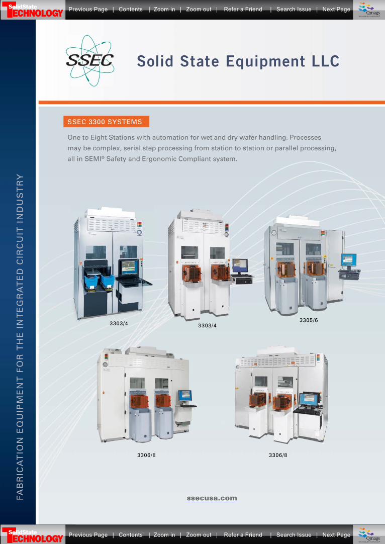
Solid State Equipment LLC
FAB
RIC
AT
ION
EQ
UIP
ME
NT
FO
R T
HE
IN
TE
GR
AT
ED
CIR
CU
IT I
ND
US
TR
Y
One to Eight Stations with automation for wet and dry wafer handling. Processes
may be complex, serial step processing from station to station or parallel processing,
all in SEMI® Safety and Ergonomic Compliant system.
ssecusa.com
SSEC 3300 SYSTEMS
3306/8 3306/8
3305/63303/43303/4
DC
qqM
Mq
qM
MqM
Qmags®THE WORLD’S NEWSSTAND
DC
qqM
Mq
qM
MqM
Qmags®THE WORLD’S NEWSSTAND
Previous Page | Contents | Zoom in | Zoom out | Refer a Friend | Search Issue | Next Page
Previous Page | Contents | Zoom in | Zoom out | Refer a Friend | Search Issue | Next Page
Page 5
S I N G L E WA F E R W E T P R O C E S S I N G A N D C L E A N I N G
© 2011 SOLID STATE LLC
Wafer Thinning≤ 2% Uniformity of Etch
with TTV Unchanged
Before Etch (Surface Roughness)
After Etch (Surface Roughness)
WET ETCH WAFER THINNING AND STRESS RELIEF
After EtchBefore Etch
UBM AND RDL METAL ETCH
PHOTORESIST AND DRY FILM STRIP
Pre-strip Post Dry Film Strip
After SSEC CleaningAfter DRIE
TSV CLEAN AND RESIST STRIP Si ETCH TO REVEAL Cu VIAS
Optical SEM
DC
qqM
Mq
qM
MqM
Qmags®THE WORLD’S NEWSSTAND
DC
qqM
Mq
qM
MqM
Qmags®THE WORLD’S NEWSSTAND
Previous Page | Contents | Zoom in | Zoom out | Refer a Friend | Search Issue | Next Page
Previous Page | Contents | Zoom in | Zoom out | Refer a Friend | Search Issue | Next Page
Page 6
F E A T U R E S
D E P A R T M E N T SC O L U M N S
OCTOBER 2012 VOL. 55 | NO. 8
2 OCTOBER 2012 SOLID STATE TECHNOLOGY www.solid-state.com
This futuristic chip, dubbed a “single chip cloud
computer” has 48 Intel cores and runs at as low
as 25 watts. Source: Intel Corp.
CO
VE
R
12
17
22
27
EMERGING ELECTRONICS | A review of recent
advances in electronic devicesHighlights from recent and upcoming conferences point to a bright future for traditional
and emerging electronics, from transistors to memory, from fl exible circuits to 3D.
Pete Singer, Editor-in-Chief
INSPECTION | Development of a CMP pad using
an unpatterned surface inspection systemWafer haze information was used to develop an advanced Cu CMP processes. C. Y. Cheng,
S. N. Peng, S.C. Chen, Semiconductor Technologies, Dow Electronic Materials, Dow Chemical
Company, Miaoli, Taiwan Larry Yang, Debbie Hu, Steve Lin, KLA-Tencor Corp., Milpitas, CA, USA
WAFER-LEVEL PACKAGING | eWLB as a cost effective
platform for 2D—3D packaging solutionsMobile product convergence leads the charge to advanced packaging technologies.
Seung Wook Yoon and Steve Anderson, STATS ChipPAC, Singapore.
CONTAMINATION CONTROL | A review of retention efficiency
measurement techniques for sub-30nm liquid filtrationA new method based on fl uorescent quantum dots was used to measure pore size.
Suwen Liu, Haizheng Zhang, Jennifer Braggin, Entegris Inc., Billerica, MA, USA
3 Web Exclusives
5 News
31 Ad Index
4 Editorial | A salute to the next generation, Pete Singer, Editor-in-Chief
12 Packaging | Progress in 3DIC SEMI standards, Dr. Phil Garrou,
Contributing Editor
16 MEMS | A visit to GE Global Research, Karen Lightman, MEMS Industry Group
32 Industry Forum | Supply chain readiness in an era of accelerated change, Karen Savala, SEMI
DC
qqM
Mq
qM
MqM
Qmags®THE WORLD’S NEWSSTAND
DC
qqM
Mq
qM
MqM
Qmags®THE WORLD’S NEWSSTAND
Previous Page | Contents | Zoom in | Zoom out | Refer a Friend | Search Issue | Next Page
Previous Page | Contents | Zoom in | Zoom out | Refer a Friend | Search Issue | Next Page
Page 7
Web Exclusives nb&news and blogs
www.solid-state.com SOLID STATE TECHNOLOGY OCTOBER 2012 3
online@ www.solid-state.com
Waiting for the next “golden year”While various industry segments appear to be tapping the
brakes, others are revving their engines and banking on
increased demand for mobile devices, observes SEMI’s
Christian Gregor Dieseldorff. Will a 2012 stall pave the way
for a record-breaking 2013? http://bit.ly/Squx9h
Secondary equipment: Turnkey
services offer a fab-centric approachRED Equipment’s Carl McMahon suggests a different model
for handling secondary semiconductor equipment for
greater ef�iciency, cost reduction, and quality control: full
turnkey services engineered to the fab’s needs without the
expense of customization. http://bit.ly/OWkK4S
iPhone 5: Which semiconductor
suppliers are the
big winners?Industry watchers sift
through the post-launch
dust cloud of Apple’s iPhone
5 debut to examine which
semiconductor suppliers gain
the most from the newest must-
have smartphone. (Hint: it helps
to be in wi-�i test, logic capex, and
sapphire.) [image via Shutterstock]http://bit.ly/PBafa4
An exclusive interview
with Lester LightbulbDr. Phil Garrou gets the inside scoop on the real problems
with LEDs and traditional light bulbs — in a one-on-one
interview with Lester Lightbulb himself.http://bit.ly/Ugqqty
28nm capacity, a
“symbiotic relation-
ship,” and a nickel hoax
Dr. Phil Garrou
blogs about
TSMC’s 28nm
yields and pos-
sible encroach-
ment into the packaging/test
realm, and a humorous twist in
the Apple-Samsung legal spat.http://bit.ly/V7ZAnK
The ConFab 2013
countdown begins
The countdown to The ConFab
has officially begun, and the
dates are set: next year’s event
will be held June 23-26, 2013
and we’ll be back at The Wynn
Las Vegas — an encore at The
Encore! http://bit.ly/Oatngt
Bosch sprouts new
market with MEMS
lawnmower
A Labor Day holiday in Maine
tied in with the German
conglomerate’s combination of
technology
from two of
its business
units: home
& garden
tools and
MEMS de-
vices. http://
bit.ly/NBRNiA
DC
qqM
Mq
qM
MqM
Qmags®THE WORLD’S NEWSSTAND
DC
qqM
Mq
qM
MqM
Qmags®THE WORLD’S NEWSSTAND
Previous Page | Contents | Zoom in | Zoom out | Refer a Friend | Search Issue | Next Page
Previous Page | Contents | Zoom in | Zoom out | Refer a Friend | Search Issue | Next Page
_____
_________________________
Page 8
4 OCTOBER 2012 SOLID STATE TECHNOLOGY www.solid-state.com
editorial
—Pete Singer, Editor-in-Chief
We make portions of our subscriber list available tocarefully screened companies that offer productsand services that may be important for your work.If you do not want to receive those offers and/orinformation, please let us know by contacting usat List Services, Solid State Technology, 98 SpitBrook Road, Nashua, NH 03062. All rights reserved.No part of this publication may be produced ortransmitted in any form or by any means, electronicor mechanical, including photocopying, record-ing, or by any information storage retrieval sys-tem, without written permission of the copyrightowner. Prices for bulk reprints of articles availableon request. Solid State Technology articles areindexed in Engineering Information and CurrentContents, and Applied Science & Technology Indexand abstracted by Applied Science & TechnologyAbstracts.
Susan Smith, Group Publisher
Ph: 603/891-9447, [email protected]
Pete Singer, Editor-in-Chief
Ph: 603/891-9217, [email protected]
James Montgomery, News Editor
Ph: 603/891-9109, [email protected]
Robert C. Haavind, Editor-at-Large
Ph: 603/891-9453, [email protected]
Julie MacShane, Copy Editor
Phil Garrou, Contributing Editor
Michael Fury, Contributing Editor
Justine Beauregard, Marketing Manager
Cindy Chamberlin, Presentation Editor
Katie Noftsger, Production Manager
Dan Rodd, Illustrator
Debbie Bouley, Audience Development
Marcella Hanson, Ad Traffic Manager
EDITORIAL ADVISORY BOARD
John O. Borland, J.O.B. Technologies
Michael A. Fury, The Techcet Group, LLC
Rajarao Jammy, SEMATECH
William Kroll, Matheson Tri-Gas
Ernest Levine, Albany NanoTech
Lars Liebmann, IBM Corp.
Dipu Pramanik, Cadence
Design Systems Inc.
Griff Resor, Resor Associates
A.C. Tobey, ACT International
EDITORIAL OFFICES
PennWell Corporation,
Solid State Technology
98 Spit Brook Road LL-1,
Nashua, NH 03062-5737;
Tel: 603/891-0123; Fax: 603/891-0597;
www.ElectroIQ.com
CORPORATE OFFICERS
1421 South Sheridan Rd., Tulsa, Ok 74112
Tel: 918/835-3161
Frank T. Lauinger, Chairman
Robert F. Biolchini, President and CEO
Mark Wilmoth, Chief Financial Officer
TECHNOLOGY GROUP
Christine A. Shaw, Senior Vice President
and Publishing Director
For subscription inquiries:Tel: (847) 559-7500; Fax: (847) 291-4816;
Customer Service e-mail: [email protected] ;
Subscribe: www.sst-subscribe.com
I’ve been working with the Semiconductor Research
Corp. (SRC) in some way for about as long as I
remember, and they’re doing very good work. By
sponsoring university-based research, they are getting
young people focused on the right kinds of research,
while also providing the guidance they need to become
industry leaders. Indeed, many of today’s leaders had
much of their education sponsored by the SRC.
For the last couple of years, we’ve been working
with the SRC to post some impromptu but interesting
video clips captured at the group’s annual TECHCON
meeting. TECHCON provides a forum to exchange
news about the progress of new materials and
processes created by SRC’s network of more than 100
of the top engineering universities.
The idea behind the videos was to capture some
unrehearsed thoughts about the SRC and various
research projects underway. Most of them are fairly
short, just a few minutes long, but that’s plenty of time
to catch the excitement of the event, and grasp the range
of projects and kinds of people involved with SRC. It’s
particularly encouraging to hear from the students and
listen to the commitment they have to their research.
We salute you!
Take a few minutes, and check them out on our
website (http://www.electroiq.com/multimedia.html).
Here’s who you’ll hear from: Ramakanth Alapati,
Global Foundries; Timothy Lu, MIT; David Pan, Univ
of Texas at Austin; Roey Shaviv, Applied Materials;
Lauren Bacigalupo, Lehigh; Xuan Liu, Carnegie Mellon;
Stephen Kosonocky, AMD; Paul Bogdan, Carnegie
Mellon; Steven Kurtz, Notre Dame; William Song,
IBM Fellow, Georgia Tech; Celia Merzbacher, SRC
Innovative Partnerships; and MaryLisabeth Rich, SRC
Education Alliance.
You’ll also hear from the two SRC award winners
from this year. Dr. Andrew Neureuther, professor
emeritus of Electrical Engineering and Computer
Science at University of California, Berkeley, the
recipient of this year’s SRC Aristotle Award; and Dr.
Jesus del Alamo, professor of Electrical Engineering
at Massachusetts Institute of Technology (MIT), the
recipient of the SRC Technical Excellence Award.
“The videos capture some
unrehearsed thoughts about
the SRC”
A salute to the next generation
DC
qqM
Mq
qM
MqM
Qmags®THE WORLD’S NEWSSTAND
DC
qqM
Mq
qM
MqM
Qmags®THE WORLD’S NEWSSTAND
Previous Page | Contents | Zoom in | Zoom out | Refer a Friend | Search Issue | Next Page
Previous Page | Contents | Zoom in | Zoom out | Refer a Friend | Search Issue | Next Page
Page 9
www.solid-state.com SOLID STATE TECHNOLOGY OCTOBER 2012 5
newsPlease send news articles to
[email protected]
worldnews
Continued on page 10
ASIA | Samsung Austin
Semiconductor says it will spend
“about $4 billion” to renovate and
retrofi t its existing facility for “full
system LSI production,” mainly to
produce mobile SoCs on 300mm
wafers using 28nm process
technologies.
ASIA | Taiwan’s top two found-
ries, TSMC and UMC, say business
picked up in the third quarter as
customers pulled in some orders.
ASIA | Samsung Electronics has
begun groundbreaking for a new
leading-edge NAND memory fab
line in Xi’an, China, to be fully on
line by 2014 making “10nm-class”
process technologies.
USA | IBM researchers have
peered further inside a molecule’s
structure to distinguish the indi-
vidual bonds, pointing the way to
building an understanding of how
graphene devices could work.
WORLD | ASML completed its
Co-Investment Program, tallying
€3.85 billion in equity funds and
€1.38B from the three biggest chip-
makers (Intel, TSMC, and Samsung)
to support R&D into EUV and
450mm.
EUROPE | Researchers at Rice U.
and the Université catholique de
Louvain in Belgium have devised
a method for converting discarded
silicon into a key material for lith-
ium-ion batteries.
EUROPE | Researchers at the
Norwegian University of Science
and Technology in Trondheim
have patented and are commer-
cializing GaAs nanowires grown on
graphene.
A delegation of stakeholders in
LED manufacturing have met with
US Department of Energy offi cials
to plead their case for increased
support in solid-state lighting (SSL)
R&D and manufacturing, with
the key message that SSL offers
greater energy conservation and
return-on-investments (ROI) than
renewable energy technologies
that get much more backing.
Pushing for the added US
backing is a delegation of SEMI
members and other industry
stakeholders with origins in the
FALCON Lighting Consortium, led
by Philips Lumileds and SEMI
members Applied Materials, Veeco,
KLA-Tencor, Ultratech, and others
(SEMI’s broad roster includes major
suppliers of LED equipment and
materials). FALCON and SEMI have
emphasized increased DOE support
Worldwide semiconductor manufacturing equipment totaled $10.34B in
2Q12, down -4% from the previous quarter and about -13% from a year
ago, according to monthly data from SEMI and SEAJ. Bookings were also
down -4% sequentially, and were off by -10% year-on-year, to $9.70B.
SEMI’s most recent forecast, issued at SEMICON West, calls for overall
chip equipment demand to slip -2.6% in 2012 to $43.53B—and only that
slightly because the two biggest end-user regions are still pushing forward,
in Korea ($11.48B, +32% and Taiwan ($9.26B, +8.6%). All other regions are
expected to reduce their equipment spending between -15% and -29%.
The fi nal SEMI/SEAJ numbers for 2Q12 support that scenario, at least
partially. Taiwan’s demand for chip tools soared 83% in 2Q12 to $3.25B,
leapfrogging the region back to the No.1 spot. Korea, meanwhile, slipped
-22% Q/Q to $2.59B, a decline-rate in line with the other sluggish regions.
“Korea’s spending was heavily weighted in 1Q, while Taiwan’s was focused
on 2Q,” explained Lara Chamness, senior market analyst for industry
research and statistics at SEMI. Assuming Samsung and Hynix stick with
their capex plans, “we would expect the second part of the year to pick
up over 2Q.” Nevertheless, she indicated the August version of SEMI’s
World Fab Forecast has adjusted equipment capex down for both Korea
(subtracting $0.9B to $10.8B) and Taiwan (subtracting $0.4B to $8.5B)—”we
do expect some softening for front-end spending in these regions.”—J.M.
LED makers urge DoE for more support
Chip tool demand slumps in
2Q12, though Taiwan shines
Continued on page 8
DC
qqM
Mq
qM
MqM
Qmags®THE WORLD’S NEWSSTAND
DC
qqM
Mq
qM
MqM
Qmags®THE WORLD’S NEWSSTAND
Previous Page | Contents | Zoom in | Zoom out | Refer a Friend | Search Issue | Next Page
Previous Page | Contents | Zoom in | Zoom out | Refer a Friend | Search Issue | Next Page
Page 10
%
-20
-10
0
10
20
30
40
2007 2008 2009 2010 2011 2012 2013 2014
6 OCTOBER 2012 SOLID STATE TECHNOLOGY www.solid-state.com
newscont.
SEMATECH researchers have
deposited extreme ultraviolet
(EUV) multi-layers with as few as
8 defects per lithography mask
at 50nm sensitivity (SiO2 equiv-
alent). The milestone shows that
tool-generated defects during
multi-layer deposition of mask
blanks used for EUV lithography
can be reduced enough to enable
high-volume manufacturing.
The team has worked for two
years to improve deposition tool
hardware, process parameters,
and substrate cleaning techniques.
Among the eight identifi ed defects
were 6 substrate defects, 1 handling
defect, and 1 defect from the
multi-layer deposition process.
This result was achieved on a 40
bi-layer fi lm stack with an Ru cap
and measured over the mask blank
quality area of 132 × 132mm2.
SEMATECH also developed
novel cleaning processes, which
improve substrate cleaning
yield on quality substrates. The
result is an integrated process
capable of manufacturing EUV
mask blanks with less than 20
total defects at 45nm sensitiv-
ity. The achievements in mask
defect reduction and increase
in yield for high-quality blanks
are attributed to a signifi cant
improvement in substrate clean-
ing, handling, and deposition.
Defects are generally formed by
SEMATECH reports EUV
cleaning breakthroughs
IHS iSuppli is downgrading its outlook for 2012 global semiconduc-
tor revenues, shifting from slight single-digit growth to predicting the
industry’s fi rst annual decline since 2009. The fi rm blames a weaken-
ing economy that has eroded demand for PCs and related components.
The decline is “a major event for the global semiconductor market,”
said Dale Ford, senior director at IHS. Even though electronics markets
remained very weak through all of 2011, the fi rm never projected a full-
year revenue dropoff, he noted. (IHS iSuppli’s original 2012 forecast
issued in January was for 3.3% growth; in April it inched that ahead to
4.3% citing strong ongoing consumer demand for wireless products
like cellphones and media tablets, but pulled back in July to 3.0%.)
Global chip revenues declined a seasonally typical -3.6% in 1Q12,
but increased barely 3% in 2Q12, attributed to the Eurozone crisis,
slowing manufacturing growth in China, and stubbornly highly
unemployment in the US. Revenue guidance from key chip suppliers
(available when this issue went to press) suggested 3Q12 would be a
slightly better 6% Q/Q growth, but that’s merely “subdued expansion”
that won’t prevent a market contraction this year, the fi rm asserts.
IHS iSuppli still feels confi dent in a strong rebound in 2013, stick-
ing with its projection of 9% Y/Y chip sales growth, assuming economic
conditions improve. Still, that optimism is qualifi ed against persistent
“multiple high-impact events” that present possible risks to create a
strong economic downturn, from the Eurozone crisis to slowing Chinese
growth to US tax and budget expirations to Middle East turmoil.—J.M.
IHS iSuppli downgrades chip market
outlook on PC weakness
Preliminary global annual semiconductor revenue growth forecast, in % change of US $. (Source: IHS iSuppli)
DC
qqM
Mq
qM
MqM
Qmags®THE WORLD’S NEWSSTAND
DC
qqM
Mq
qM
MqM
Qmags®THE WORLD’S NEWSSTAND
Previous Page | Contents | Zoom in | Zoom out | Refer a Friend | Search Issue | Next Page
Previous Page | Contents | Zoom in | Zoom out | Refer a Friend | Search Issue | Next Page
Page 11
Learn more:http://indium.us/E024
Visit my semiconductor blog
for the latest on:
������������ ����
���������������
�����������������������������
��!����
SemiconductorAssembly
Andy C. MackiePhD, MScGlobal Product
Manager
[email protected]
©2012 Indium Corporation
" # $ " � � � % & $ ' " � � � ( ) * + � ( � � � ) # "
www.indium.com
[email protected]
www.solid-state.com SOLID STATE TECHNOLOGY OCTOBER 2012 7
decoration of substrate defects by
the multilayer deposition process
and, to a lesser extent, by the
deposition process itself. Defects
prevent mask blanks from keeping
pace with roadmap requirements
for the production of pilot line and
high-volume manufacturing EUV
reticles. Substrate and mask blank
defect levels have steadily improved
across the industry, but more
slowly than expected. Reducing
defects in EUV mask blank multi-
layer deposition system is one of
the most critical technology gaps
the industry needs to address to
enable cost effective insertion of
this technology at the 22nm half-
pitch. For successful introduction,
integrated EUV blanks must meet a
defectivity level of less than 0.003
defects/cm2 at 25nm sensitivity.
A low defect density refl ec-
tive mask blank is considered to be
one of the top two critical technol-
ogy gaps for commercialization
of EUVL technology, according
to Frank Goodwin, manager of
SEMATECH’s Mask Blank Defect
Reduction program. “The goal
of our work is to enable model-
based prediction and data driven
analysis of defect performance
for targeted process improve-
ment and component learning
to feed into the new deposition
tool design,” he stated.—M.C.
lithography mask defect,
DC
qqM
Mq
qM
MqM
Qmags®THE WORLD’S NEWSSTAND
DC
qqM
Mq
qM
MqM
Qmags®THE WORLD’S NEWSSTAND
Previous Page | Contents | Zoom in | Zoom out | Refer a Friend | Search Issue | Next Page
Previous Page | Contents | Zoom in | Zoom out | Refer a Friend | Search Issue | Next Page
Page 12
20122011 20122011
Monthly
change
-15
-10
-5
0
5
10
15
JJMAMFJDNOSAJ-20
-15
-10
-5
0
5
10
15
20
JJMAMFJDNOSAJ
EuropeJapanAsia PacificAmericas
EuropeJapanAsia Pacific
Americas
Yearly
change
*Based on a three-month moving average
% %
8 OCTOBER 2012 SOLID STATE TECHNOLOGY www.solid-state.com
newscont.
Global semiconductor sales totaled $24.34B in July, a
scant 0.2% increase from the prior month and down
-1.9% from a year ago, as macroeconomic challenges
weigh down demand particularly in Europe and the
Americas, according to the latest monthly data from
the Semiconductor Industry Association (SIA).
“July’s sales figures offer some encouraging signs
for the global semiconductor industry, but it’s clear
that macroeconomic challenges are restricting stron-
ger growth,” stated Brian Toohey, SIA president & CEO.
On a positive note, the year/year decrease was
actually smaller than it has been since Oct. 2011, the
SIA noted. June semiconductor sales were flat from
May thanks to declines in the Americas and Europe,
and down -2% from the same month a year ago.
The regional outlook remains uneven, with Japan rebound-
ing from last year’s disaster and the Asia-Pacific region
holding steady, but Europe and the Americas are lagging
behind. Japan (4.2%) and the Asia-Pacific (1.4%) showed
year-on-year growth, but both Europe and the Americas
saw around -10% declines. Likewise on a sequential monthly
basis, Japan (5.4%, its strongest M/M increase in three
years) and Asia-Pacific (0.3%) were positive, but Europe
was flat and the Americas declined from June (-3.9%). All
numbers represent a three-month moving average.—J.M.
SIA: July semiconductor salesinch up, unevenly
Worldwide semiconductor sales growth by region.(Source: SIA/WSTS)
worldnews
USA | The National Institute of Standards and
Technology (NIST) says a “Bayesian approach”
combining scanning techniques with statistical
data can more precisely and less expensively
measure features on a chip—and it claims IBM
and GlobalFoundries are on board.
WORLD | Demand for power management
semiconductors recovered in 2Q12 after declin-
ing for half a year, thanks to strong demand from
electronic products such as smartphones and
media tablets, according to IHS iSuppli.
ASIA | Taiwanese DRAM manufacturer Nanya
Technology has received a $27M equity invest-
ment from a subsidiary of Integrated Silicon
Solution.
WORLD | UMC and STMicroelectronics are
extending their work in CMOS image sensors to
include 65nm backside illumination (BSI) tech-
nology, targeting applications including smart-
phones and tablets.
ASIA | STATS ChipPAC has expanded its
through-silicon via (TSV) capabilities with a
300mm mid-end manufacturing operation.
WORLD | Despite the gloomy economy and soft-
ness in consumer LCD products, TFT-LCD suppli-
ers expect moderate growth (8%-13%) in 2012, to
$85B and 757M units, according to DisplaySearch.
WORLD | Tokyo Electron Ltd. is acquiring FSI
International for approximately $252.5 million.
USA | FormFactor is acquiring Microprobe in a
$116M cash-and-stock deal that combined would
rival Micronics as the top probe card supplier.
USA | MEMS timing firm Sand 9 has landed
a $3M investment from mobile gear giant
Ericsson.
ASIA | An unidentified “premier global indus-
try research center in Asia” will use Rudolph
Technologies’ MetaPulse G metrology system
in its advanced packaging process development
activities.
Continued from page 5
Continued on page 10
DC
qqM
Mq
qM
MqM
Qmags®THE WORLD’S NEWSSTAND
DC
qqM
Mq
qM
MqM
Qmags®THE WORLD’S NEWSSTAND
Previous Page | Contents | Zoom in | Zoom out | Refer a Friend | Search Issue | Next Page
Previous Page | Contents | Zoom in | Zoom out | Refer a Friend | Search Issue | Next Page
Page 13
012
VAC
UU
MVA
LV
ES
20
VAC
UU
MVA
LV
ES
201
VAC
UU
MVA
LV
ES
2012
012
012
Catalog
Request your copy today!
www.vatvalve.com
Transfer
valves
Control
valves
Angle
valves
Gate
valves
www.vatvalve.com
Swiss Headquarters
[email protected]
VAT Benelux
[email protected]
VAT Japan
[email protected]
VAT France
[email protected]
VAT Korea
[email protected]
VAT Germany
[email protected]
VAT Taiwan
[email protected]
VAT U.K.
[email protected]
VAT China
[email protected]
VAT USA
[email protected]
VAT Singapore
[email protected]
8
4
0
-4
1Q 2Q 3Q 4Q
-8
12
30-yr average
Excluding 4Q08,4Q avg. would be 3.7% Excluding 4Q08,
4Q avg. would be 2.1%
Avg. growth in 14good* years
Avg. growth in 16poor* years
*≥10% annual growth
**<10% annual growthTime period
% change
In an analysis of quarterly IC market growth rates, IC Insights pulls up this
phenomenon: the performance during the second calendar quarter takes
the spotlight in years of better growth, which is counter to historical norms.
Averaging IC market growth over the past 30 years, the third quarter
saw the highest Q/Q increase at almost 6%, while 1Q was typically the
softest (-1.4%)—nothing surprising there, given seasonal trends of a
pre-holiday-season pickup and then letdown. But dividing the results
into “good” vs. “bad” years for the IC marketplace (defined as ±10%
annual growth) surfaced a curious trend. In bad years, the first half of
the year typically takes the brunt of the slowdown, while the second half
usually rebounds. In good years, however, the second quarter typically
shows the highest sequential growth rate, with 3Q and 4Q slowing but
still healthy, and even typically-soft 1Q levels staying in the black (3.1%).
Another trend the firm teases out of the data: the IC market is becom-
ing increasingly dependent upon seasonal growth in 3Q12. (Not surpris-
ing as electronic systems sales have shifted more heavily from business
to consumers in the past few decades.) Two of today’s biggest markets are
PCs and cellphones, both of which are highly seasonal in nature. Bottom
line: expect the IC market to continue its pattern of stronger 3Q seasonality.
Meanwhile, 4Q IC sales have been trending down for the better part of
three decades—though in 2012 the expected introduction of new products
(smartphones, tablet PCs, ultrabooks) timed for late 3Q12 might give 4Q12
sales a rare sequential boost, by as much as 3% this year, the firm notes.—J.M.
Why 2Q makes or breaks a “good” year for IC sales
Average sequential quarterly IC market growth rates, 1983-2012 (f).(Courtesy of IC Insights)
DC
qqM
Mq
qM
MqM
Qmags®THE WORLD’S NEWSSTAND
DC
qqM
Mq
qM
MqM
Qmags®THE WORLD’S NEWSSTAND
Previous Page | Contents | Zoom in | Zoom out | Refer a Friend | Search Issue | Next Page
Previous Page | Contents | Zoom in | Zoom out | Refer a Friend | Search Issue | Next Page
Page 14
10 OCTOBER 2012 SOLID STATE TECHNOLOGY www.solid-state.com
newscont.
for domestic SSL development and
especially manufacturing. US LED
manufacturing received over $23M
in grants in several areas (metrol-
ogy, lithography, and deposition
R&D) under the 2009
American Recovery
and Reinvestment
Act; funding has been
reduced since then, but
lobbying efforts have
restored and increased
funding levels above
what the DoE submit-
ted to appropriations
subcommittees.
This August the
groups met with US DoE Assistant
Secretary of Energy David Danielson
and his senior staff, their fi rst such
meeting in recent years. The key
message was that energy conser-
vation achieved through SSL can
have a greater impact on US energy
than renewable energy technolo-
gies which currently get government
investments (and a lot more of it).
The group calculates SSL can deliver
4.0-6.0 quads of annual energy
savings for a 10-20× higher ROI than
other energy investment alternatives.
“According to the Energy
Information Administration, on a
dollar-per-unit of-production basis,
the level of subsidies received by
the wind and solar industries were
almost 100 times greater than those
for conventional energy,” stated
Richard Solarz, senior director of
technology at KLA-Tencor and
Randy Moorhead, VP for govern-
ment relations at Philips Electronics,
co-leaders of the group advocating
for greater DOE support for SSL.
“We believe that it is
generally understood that
conventional energy conser-
vation—specifi cally lighting—
efforts are under-supported.”
SEMI added that it hopes the
meeting will help secure support for
SSL beyond its funding levels of the
past four years, despite the obvious
and formidable pressures on national
budgets. “Despite the austerity mood
in Washington, SEMI is confi dent
that increased budget requests for
LED-based lighting technologies will
receive considerable bicameral and
bipartisan support in the legislative
branch during upcoming legislative
sessions,” the group stated.—J.M.
ProgramFY11 DOE
request ($K)
2009 generation
(quads), US*
2035 generation (quads)
projected, US
2035 relative
investment per quad
Solar $302,398 0.068 4.7 (EIA est.) 1
Hydro $40,488 2.7 2.7 (www.grist.org) 0.23
Geothermal $55,000 0.38 1.5 (DOE MYPP-MIT study) 2.25
Biomass $220,000 2.01 4.3 (EIA est.) 0.8
Wind $122,500 0.692.12
(renewableenergyfocus.com)0.9
Lighting $26,809 6.0/4.0** (savings) 6.0/4.0** (savings) 0.1
*US EIA 2009 Annual Energy Review
** January 27, 2012 DOE est. 4.0 quads, FALCON estimate against current usage 6.0 quads
Continued from page 5
worldnews
EUROPE | A new laser process
devised by Innolas, FiLaser, and
Lumera Laser enables faster, more
cost-effi cient production of cover
glasses, FPDs, and LEDs.
WORLD | US-based investment
fi rm Kohlberg Kravis Roberts (KKR)
reportedly is seeking to snap up
struggling chip fi rm Renesas for ¥100
billion (US $1.3B)
WORLD | TSMC has joined IMS’ mul-
tibeam mask writer development
collaboration to develop an elec-
tron multi-beam mask writer, joining
founding members DNP, Intel, and
Photronics.
USA | Matheson has acquired a
majority stake in RASIRC, supple-
menting its gas purifi cation and mate-
rial businesses with RASIRC’s water
vapor systems.
JAPAN | UMC will close its fab opera-
tion in Japan and dissolve subsidiary
UMC Japan.
Continued from page 8
DC
qqM
Mq
qM
MqM
Qmags®THE WORLD’S NEWSSTAND
DC
qqM
Mq
qM
MqM
Qmags®THE WORLD’S NEWSSTAND
Previous Page | Contents | Zoom in | Zoom out | Refer a Friend | Search Issue | Next Page
Previous Page | Contents | Zoom in | Zoom out | Refer a Friend | Search Issue | Next Page
________________
Page 15
Packaging
www.solid-state.com SOLID STATE TECHNOLOGY OCTOBER 2012 11
The Inspection and Metrology Task Force of the
SEMI 3D standards group, recently approved its first
Standard,SEMI 3D1, Terminology for Through Silicon
Via Geometrical Metrology.
SEMI 3D1 will provide a starting point for standard-
ization of geometrical metrology for selected dimen-
sions of through silicon vias (TSVs). Although different
technologies can measure various geometrical param-
eters of an individual TSV, or of an array of TSVs,
such as pitch, top diameter, top area, depth, taper (or
sidewall angle), bottom area, and bottom diameter,
it is currently difficult to compare results from the
various measurement technologies as parameters
are often described by similar names, but actually
represent different aspects of the TSV geometry.
Other standards under development by the
Inspection and Metrology Task Force include SEMI Draft
Document 5270, Guide for Measuring Voids in Bonded Wafer
Stacks, SEMI Draft Document 5409, Guide for Metrology
for Measuring Thickness, Total Thickness Variation (TTV),
Bow, Warp/Sori, and Flatness of Bonded Wafer Stacks, SEMI
Draft Document 5410, Guide for Metrology Techniques
to be used in Measurement of Geometrical Parameters of
Through-Silicon Vias (TSVs) in 3DS-IC Structures, and SEMI
Draft Document 5447, Terminology for Measured Geomet-
rical Parameters of Through-Glass Vias (TGVs) in 3DS-IC
Structures.
The Thin Wafer Handling Task Force is focused
defining thin wafer handling
requirements including
physical interfaces used in
3D-IC manufacturing. Current
standards for shipping are not
well-suited for the reliable storage
and transportation of thin wafers
and dice on tape frames used
in 3D-IC manufacturing. Wafer
thicknesses of 30-200μm will
need significant changes to the
current design criteria of current wafer transport and
storage containers. SEMI Draft Document 5175 aims to
address the robust handling and shipping of thin wafers,
including changes in securing the wafers.
The Bonded Wafer Stacks Task Force is near
completion of its SEMI Draft Document 5173, Guide
for Describing Materials Properties and Test Methods for a
300 mm 3DS-IC Wafer Stack and SEMI Draft Document
5174, Specification for Identification and Marking for
Bonded Wafer Stacks.
Current wafer standards do not adequately address
the needs of wafers used in three-dimensional bonded
wafer stacks for stacked integrated circuits. In each
step of a 3D-IC process, the incoming material must be
specified in terms of wafer dimension and materials
present. Wafer thickness, edge bevel, notch, mass,
bow/warp and diameters change when wafer stacks
are bonded, debonded, and when wafers incorporated
into stacks are thinned. Further, these parameters will
change for a single wafer stack during process. This
Document will provide the required properties of both
silicon (“device”) wafers and glass (“carrier”) wafers to
be used in 3D-IC applications. Templates for describing
bonded wafer stacks and processed wafers to be used
in the bonding flow would be provided as well.
The Middle-End Task Force is focused on the middle-
end processes on wafers with or without TSVs, including
post-final metal temporary bonding, wafer thinning,
TSV formation and reveal, micro-bumping, redis-
tributed line formation and carrier de-bond. The task
force’s first two proposals are SEMI Draft Document
5473, Guide for Alignment Mark for 3DS-IC Process, and
SEMI Draft Document 5474, Guide for CMP and Micro-
bump Processes for Frontside TSV Integration. Th e group
that developed SEMI 3D1 continues to develop
standards to be used in measuring the properties of
TSVs, bonded wafer stacks and dies. �
Progress in
3DIC SEMI
standards
Dr. Phil Garrou,
Contributing Editor
DC
qqM
Mq
qM
MqM
Qmags®THE WORLD’S NEWSSTAND
DC
qqM
Mq
qM
MqM
Qmags®THE WORLD’S NEWSSTAND
Previous Page | Contents | Zoom in | Zoom out | Refer a Friend | Search Issue | Next Page
Previous Page | Contents | Zoom in | Zoom out | Refer a Friend | Search Issue | Next Page
Page 16
12 OCTOBER 2012 SOLID STATE TECHNOLOGY www.solid-state.com
The FinFET has grabbed the limelight when
it comes to next-generation electronics,
and further advances continue to be made,
particularly by Intel. At the upcoming Inter-
national Electron Devices Meeting (IEDM)
in December, the company plans to show how they
have developed a complete platform for system-
on-chip (SoC). But that’s just one of the exciting
announcements to come from IEDM and other
conferences, such as the VLSI Symposium held
in June.
Tremendous advancements have been made in
building advanced circuits on fl exible substrates, for
example, which could some day lead to roll-to-roll
processing of ICs. To date, fl exible circuits have off ered
limited performance because plastic substrates aren’t
compatible with the high temperatures and harsh
processes needed to make high-performance CMOS
devices. At IEDM, for the fi rst time, a way around this
will be unveiled. IBM researchers will demonstrate
high-performance state-of-the-art CMOS circuits —
including SRAM memory and ring oscillators—on a
fl exible plastic substrate.
IBM used extremely thin silicon on insulator
(ETSOI) devices, with a body thickness of just 60
angstroms. IBM built them on silicon and then used
a simple, low-cost room-temperature process called
controlled spalling. Th en they transferred them to
fl exible plastic tape.
Th e devices had gate lengths of <30nm and gate pitch
of 100nm. Th e ring
oscillators had a stage
delay of just 16ps
at 0.9V, believed to
be the best reported
performance for a
fl exible circuit.
imec, the Belgium-based consortium, also recently
announced that it has integrated an ultra-thin, fl exible
chip with bendable and stretchable interconnects into a
package that adapts dynamically to curving and bending
surfaces (Figure 1). Th e resulting circuitry can be
embedded in medical and lifestyle applications where user
comfort and unobtrusiveness is key, such as wearable
health monitors or smart clothing.
New fl avors of FinFETS
Multiple-gate transistors, such as the FinFET (or
“trigate” transistors as known by Intel) provide superior
on/off control, enabling high drive currents to be
achieved at a lower supply voltage than otherwise.
At IEDM, Intel will discuss how it developed several
FinFET “families” of high-speed, low-standby-power
and high-voltage-tolerant devices (Figure 2), combined
with state-of-the-art interconnects and RF/mixed-
signal features for a wide range of SoC applications.
Th e high-speed logic transistors have subthreshold
leakages ranging from 100nA/μm to 1nA/μm, while
the low-power versions feature leakage of < 50pA/μm
yet have drive currents 50% higher than 32nm planar
FIGURE 1. imec has integrated an
ultra-thin, fl exible chip with bendable
and stretchable interconnects into a
package that adapts dynamically to
curving and bending surfaces.
A review of recent advances
in electronic devices
PETE SINGER, Editor-in-Chief
Highlights from recent and upcoming conferences point to a
bright future for traditional and emerging electronics, based
on silicon, fl exible substrates, graphene and nanowires.
EMERGING ELECTRONICS
DC
qqM
Mq
qM
MqM
Qmags®THE WORLD’S NEWSSTAND
DC
qqM
Mq
qM
MqM
Qmags®THE WORLD’S NEWSSTAND
Previous Page | Contents | Zoom in | Zoom out | Refer a Friend | Search Issue | Next Page
Previous Page | Contents | Zoom in | Zoom out | Refer a Friend | Search Issue | Next Page
Page 17
reduce soft errors
Deliver more density on your IC packages without soft errors.Honeywell RadLo™ low alpha packaging materials
help eliminate soft errors and single event upsets
by reducing alpha emissions, a significant source
of these problems. This is becoming increasingly important as chip dimen-
sions and designs continue to miniaturize. Our leadership and expertise in
low alpha refining and metrology mean that Honeywell can help you meet
critical alpha emission levels.
Honeywell reliability. Reliable low alpha. Make sure to
ask your suppliers if they are using Honeywell RadLo low alpha materials
for their chip packaging processes.
Find out more by visiting us at www.honeywell-radlo.com
Although all statements and information contained herein are believed to be accurate and reliable, they are presented without guarantee or warranty of any kind, express or implied. Information provided herein does not relieve the user from the responsibility of carrying out its own tests and experiments, and the user assumes all risks and liability for use of the information and results obtained. Statements or suggestions concerning the use of materials and processes are made without representation or warranty that any such use is free of patent infringement and are not recommendations to infringe any patent. The user should not assume that all toxicity data and safety measures are indicated herein or that other measures may not be required. ©2012 Honeywell International Inc. All rights reserved.
www.solid-state.com SOLID STATE TECHNOLOGY OCTOBER 2012 13
(traditional technology) devices. Th e
process also yields high-voltage
transistors (1.8V or 3.3V) for analog
circuits, I/O, legacy designs and other
applications. Th ey feature the highest
reported I/O device drive currents
for an SoC technology (NMOS/
PMOS=0.92/0.8mA/μm at 1.8V).
Th e trigate technology platform also
features eight to 11 layers of low-k
and ultra-low-k carbon-doped oxide
(CDO) interconnect at tight pitches for
diff erent applications; many analog/
mixed-signal features; and three
diff erent SRAM bit cells, spanning
high-density/low-leakage (0.092μm2),
low voltage (0.108μm2) and high-
performance (0.130μm2).
ETSOI
Another exciting development in the
transistor world is extremely thin
SOI (ETSOI) technology, which is
quickly emerging as a viable device
architecture for continued CMOS
scaling to 22nm and beyond. It off ers
superior short-channel control and
low device variability with undoped
channels. At the IEDM, a team led by
IBM will report on the world’s fi rst
high-performance hybrid-channel
ETSOI CMOS device (Figure 3). Th ey
integrated a PFET having a thin,
uniform strained SiGe channel, with an NFET having
a Si channel, at 22nm geometries. A novel STI-last
process makes the hybrid architecture possible. Th e
researchers built a ring oscillator circuit to benchmark
performance, and the hybrid planar devices enabled
the fastest ring oscillator ever reported, with a delay of
only 11.2ps/stage at 0.7V, even better than FinFETs.
FIGURE 2. Intel will roll out two
versions of its tri-gate transistor, one
for logic (top) and the other for high
voltage (bottom), all integrated into
an SoC. Source: Intel.
DC
qqM
Mq
qM
MqM
Qmags®THE WORLD’S NEWSSTAND
DC
qqM
Mq
qM
MqM
Qmags®THE WORLD’S NEWSSTAND
Previous Page | Contents | Zoom in | Zoom out | Refer a Friend | Search Issue | Next Page
Previous Page | Contents | Zoom in | Zoom out | Refer a Friend | Search Issue | Next Page
Page 18
14 OCTOBER 2012 SOLID STATE TECHNOLOGY www.solid-state.com
EMERGING ELECTRONICS
Future memories
While conventional charge-based
memory is approaching funda-
mental scaling limits, several
so-called “emerging memories” have migrated from
laboratory samples to integrated products. Among
various emerging memory technologies, MRAM
(magnetoresistive random access memory) has been
making impressive progress, ahead of other emerging
memories, and has demonstrated the capability to
be a successor to DRAM or SRAM. MRAM data is
stored via magnetic moments. Parallel or anti-parallel
magnetic moments in MRAM stacks present the “0”
or “1” state. In earlier generations of MRAM, these
states were switched by current-induced magnetic fi eld
but that is an obstacle for scaling. Th e invention of ST
(spin-torque) MRAM, which is switched by injecting
spin-polarized tunneling current, removes the scaling
limitation. At IEDM, in an invited paper, researchers
from Everspin Technologies will describe how they
built the largest functional ST-MRAM circuit ever built,
a 64Mb device with good electrical characteristics. Th e
work shows that MRAM technology is fast approaching
commercialization.
Earlier this year, at the VLSI Technology Symposium
(Honolulu, Hawaii), imec presented signifi cant
improvements in performance and reliability for a type
of non-volatile called resistive RAM (RRAM).
RRAM is a promising concept for future non-volatile
memories because of its high speed, low energy
operation, superior scalability, and compatibility
with CMOS technology. Its operation relies on the
voltage controlled resistance change of a conductive
fi lament in the dielectric of a Metal/Insulator/Metal
(MIM) stack. RRAM systems based on HfO2 have been
demonstrated to have excellent scaling capabilities
(area <10x10nm) and strong reliability due to effi cient
voltage-controlled management of oxygen motion in
the stack during switching.
Progress in more conventional
memory technology also continues,
particularly in 3D memories. At
IEDM, the fi rst working 3D NAND
fl ash memory at sub-40nm feature
sizes will be described by Macronix
researchers. Th ey used vertical
gates having horizontal channels
to create a new architectural layout
that dramatically decreases feature
sizes in the wordline direction and
improves manufacturability. Th e new architecture also
enables the use of a novel “staircase” bitline contact
formation method to minimize fabrication steps and
cost. Th e result is an eight-layer device with a wordline
feature size of 37.5nm, bitline feature size of 75nm,
64 cells per string and a core array effi ciency of 63%.
Th e researchers say the technology not only is lower
cost than conventional sub-20nm 2D NAND, but it
can provide 1 Tb of memory if further scaled to 25nm
feature sizes. At that size the Macronix device would
comprise only 32 layers, compared to 3D stackable
NANDs with vertical channels that would need almost
100 layers to reach the same memory density.
Graphene, MoS and nanowires
No discussion of emerging electronics would be
complete without an update on graphene, and an
exciting alternative. Graphene is seen as a potential
replacement for silicon in future transistors because
it has an exceptional set of properties (high current
density, mobility and saturation velocity). However,
transistors made of graphene cannot be turned
off because graphene has almost no band gap.
Researchers have begun to inves-
tigate a new 2D
material—molyb-
denum sulfi de
(MoS)—which
has similar
characteristics but
off ers something
graphene doesn’t:
a wide energy
bandgap, enabling
transistors and
FIGURE 3. An electron microscope
view is shown at the top and an EDX
(energy-dispersive X-ray) spectroscopic
view below it of a SiGe-channel PFET
with 6-nm channel thickness, 22nm gate
length, 100-nm contacted gate pitch,
high-k/metal gate architecture and ISBD
SiGe raised source drain. Source: IBM.
FIGURE 4A. A computer
simulation showing the structure
of the optimized ambipolar silicon
nanowire device structure, with
three 45-nm-long gate regions.
DC
qqM
Mq
qM
MqM
Qmags®THE WORLD’S NEWSSTAND
DC
qqM
Mq
qM
MqM
Qmags®THE WORLD’S NEWSSTAND
Previous Page | Contents | Zoom in | Zoom out | Refer a Friend | Search Issue | Next Page
Previous Page | Contents | Zoom in | Zoom out | Refer a Friend | Search Issue | Next Page
Page 19
Two strong brands combined for your success
� Best-in-class products� Leading vacuum technology know-how� Worldwide sales and service support
Are you looking for a perfect vacuum solution?
Please contact us:
Pfeiffer Vacuum GmbH
Headquarters/GermanyT +49 6441 802-0F +49 6441 802-1202 [email protected]
www.pfeiffer-vacuum.com
Perfect Vacuum Solutions!
A PA S S I O N F O R P E R F E C T I O N
Extended product portfolio
now online!
www.solid-state.com SOLID STATE TECHNOLOGY OCTOBER 2012 15
EMERGING ELECTRONICS
circuits to be built from it directly. At
IEDM, an MIT-led team will describe
the use of CVD processing to grow
uniform, flexible, single-molecular
layers of MoS, comprising a layer of
Mo atoms sandwiched between two
layers of S atoms. They exploited the
material’s 1.8 eV bandgap to build
MoS transistors and simple digital
and analog circuits (a NAND logic
gate and a 1-bit ADC converter). The
transistors demonstrated record MoS
mobility (>190cm2/Vs), an ultra-high
on/off current ratio of 108, record
current density (~20μA/μm) and
saturation, and the first GHz RF
performance from MoS.
Another important devel-
opment to be unveiled at IEDM:
The phenomenon of
ambipolar conduction
(the ability to switch
between N- or
P-type), which has
been observed in some
nanoscale transistors made
from silicon, carbon and graphene.
A team led by researchers from the
Swiss Federal Institute of Technology
in Lausanne (EPFL) built gate-all-
around ambipolar Si nanowire FETs
in a vertically stacked configuration
on an SOI substrate (Figure 4). A
“polarity gate” attached to the ends of the nanowires
is used to switch their polarity dynamically between
the N and P states, while a control gate in the middle
turns them on or off. The devices showed an excellent
on/off current ratio of 106 and subthreshold slope of
70mV/dec. The researchers built a logic gate to show the
technique’s usefulness for future logic design. �
FIGURE 4B. This image is a tilted
SEM (scanning electron microscope)
view of the nanowire stacks after
deposition and etching of the polarity
gate structures.
DC
qqM
Mq
qM
MqM
Qmags®THE WORLD’S NEWSSTAND
DC
qqM
Mq
qM
MqM
Qmags®THE WORLD’S NEWSSTAND
Previous Page | Contents | Zoom in | Zoom out | Refer a Friend | Search Issue | Next Page
Previous Page | Contents | Zoom in | Zoom out | Refer a Friend | Search Issue | Next Page
Page 20
16 OCTOBER 2012 SOLID STATE TECHNOLOGY www.solid-state.com
MEMS
Perched on a bluff overlooking the Mohawk River in
Niskayuna, NY is a powerhouse of industrial R&D; GE’s
Global Research Center (GRC). GRC just celebrated its
110 year anniversary. Thomas Edison’s original desk is
on display in the entry lobby to prove this point!
Th e Niskayuna facility is the largest of several GRCs.
GE also has centers in Munich, Germany; Bangalore,
India; Shanghai, China; Rio de Janeiro, Brazil and San
Ramon, California.
Th e history of invention and innovation that has
taken place at GRC to create major new businesses was
on display as we walked along the entry hall. Some
highlighted examples include x-ray medical imaging,
jet engines, magnetic resonance imagers, digital
x-ray panels and a number of other world fi rsts. Th e
Research Center in Niskayuna is one of the world’s
largest corporate R&D centers that conducts focused,
strategic research and development.
GRC has been conducting research in MEMS
since 2002. Th e objective of this research is to create
new MEMS components that are not commercially
available and that enable a breakthrough feature or
strengthen the value proposition of a GE product.
One of the most impressive MEMS devices that I
learned about at GRC is a MEMS microswitch --
GRC researchers claim this switch to be the fastest
switch that acts as a mechanical relay (vs. solid
state, semiconductor switches). Th rough applied and
focused R&D, the brilliant scientists at GRC have
created a MEMS microswitch that handles over a
kilowatt of power (240 Volts AC and 7
Amps). For its industrial applications
(just for starters) this MEMS microswitch
reduces the time required to interrupt a
fault current (short circuit) from
milliseconds (the switching
speed of conventional circuit
breakers) to a few microseconds
(for a breaker made from MEMS
switches).
It is equally amazing that
these researchers were able to
utilize a novel set of materials
to construct the MEMS switches (GRC’s “secret
sauce”). Th e switch materials and the process fl ow are
compatible with both silicon and quartz substrates,
and it may be possible to fabricate these switches on
completed CMOS wafers. Th e novel materials play
a key role in enabling the fabrication of the robust,
reliable and mega-power-conveying MEMS micro-
switches. In addition, GRC also does all the failure
mode analysis, reliability testing, and most of the
packaging for the microswitches; as well as most of
the other MEMS they R&D and fab onsite. It’s quite
an impressive operation.
But what makes GRC unique is that for MEMS,
not only do these guys do the R&D at GRC, they
also do the pilot volume fabrication. With their new
expanded cleanroom facility (nearly 30,000 sq. ft.);
they are doing amazingly cool stuff in MEMS. From
what I learned on the full head-to-toe bunny suit tour
that I had with fab manager, Ron Olson, GRC is fabri-
cating both silicon carbide based power MOSFETs
and MEMS for GE at an impressive rate. By no means
is this a high-volume fab; but these guys have a
sophisticated operation that is able to accommodate
both the R&D and the pilot volume needs of GE’s
businesses in a single facility.
Lastly, no visit to the facility can be complete
without a mention of the beauty of the place. It truly
is gorgeous, especially in July. Th e rate of turnover at
GRC is low and I can see why; why would you want to
leave this place? You get to work with brilliant scien-
tists, doing great commercially focused R&D, actually
manufacture products and live in a beautiful part of
the country. As Th omas Edison once stated: “I never
perfected an invention that I did not think about in
terms of the service it might give to others.” Clearly at
GRC Niskayuna, his legacy lives on. �
A visit to GE
Global Research
Karen Lightman, Managing Director,
MEMS Industry
Group
DC
qqM
Mq
qM
MqM
Qmags®THE WORLD’S NEWSSTAND
DC
qqM
Mq
qM
MqM
Qmags®THE WORLD’S NEWSSTAND
Previous Page | Contents | Zoom in | Zoom out | Refer a Friend | Search Issue | Next Page
Previous Page | Contents | Zoom in | Zoom out | Refer a Friend | Search Issue | Next Page
Page 21
www.solid-state.com SOLID STATE TECHNOLOGY OCTOBER 2012 17
As design rules continue to shrink, copper
chemical mechanical polishing (CMP) remains
a challenging component of copper dual
damascene processes. Traditionally, inspection
of blanket wafers to determine how diff erent
factors infl uence overall defectivity has been used
for CMP process development. In this study, wafer
haze information is used to reveal defect signatures
not apparent on standard defect maps. New methods
of advanced haze analysis are used to measure haze
defects on copper blanket wafers for characterization
and development of CMP pads.
Introduction
Chemical mechanical polishing is a critical process
for wafer surface global and local planarization in IC
manufacturing. Copper (Cu) CMP has been widely
reported as one of the leading techniques for Cu inter-
connect applications [1]. Blanket wafer inspection has
played a key role in helping engineers optimize Cu
CMP processes. In the past, the standard blanket wafer
defect detection system for CMP process es focused
on particle or scratch count and characterization.
However, the standard methodology is no longer
suitable for detecting anomalous process defects while
technology nodes continue to scale down. Accessing
defectivity information below standard thresholds can
be achieved by wafer haze analysis, which represents a
powerful tool for capturing spatial signatures caused
by CMP processes [2,3]. As such, wafer haze infor-
mation can be used in addition to standard defectivity
data to optimize CMP processes and characterize CMP
defects.
Th e unpatterned wafer surface inspection system
used in this study (KLA-Tencor’s Surfscan SP2) works
by scanning a laser spot over the surface of a wafer
with normal, oblique, or dual incidence and then
collecting the scattered light into wide and narrow
collection channels. From that scattering signal, both
light point defects (LPDs) and haze can be extracted.
Th e LPD information is used to generate a map of
localized defects — the predominant information
gathered from a system of this sort. Th e haze portion
of the signal is often regarded as nuisance when
localized defects are the aim of the measurement. As
a result, grazing angle systems with sophisticated
algorithms were designed to suppress haze. Th e wafer
manufacturers and their users discovered that haze
maps also contain important information because
haze correlates with surface roughness. However, the
value of haze information has been limited by lateral
resolution and sensitivity, the lack of haze standards,
Development of a CMP
pad using an unpatterned
surface inspection system
C. Y. CHENG, S. N. PENG, S.C. CHEN, Semiconductor Technologies, Dow Electronic Materials, Dow Chemical Company,
Miaoli, Taiwan. LARRY YANG, DEBBIE HU, STEVE LIN, KLA-Tencor Corp., Milpitas, CA, USA
Wafer haze information was used to develop advanced Cu CMP processes.
INSPECTION
C. Y. CHENG is a metrology engineer ([email protected] ), S. N. PENG is a technology center lab manager, and S. C. CHEN is a
process engineer at Dow Electronic Materials, Dow Chemical Company, and LARRY YANG is an application engineer, DEBBIE HU is a
regional product manager, and STEVE LIN is an application manager with KLA-Tencor Corp.
DC
qqM
Mq
qM
MqM
Qmags®THE WORLD’S NEWSSTAND
DC
qqM
Mq
qM
MqM
Qmags®THE WORLD’S NEWSSTAND
Previous Page | Contents | Zoom in | Zoom out | Refer a Friend | Search Issue | Next Page
Previous Page | Contents | Zoom in | Zoom out | Refer a Friend | Search Issue | Next Page
Page 22
4500
Pad 1
Pad 1 Batch X Batch YPad 2 Pad 3 Pad 4 All pairsTukey-Kramer
0.05
All pairsTukey-Kramer
0.05
All pairsTukey-Kramer
0.05
All pairsTukey-Kramer
0.05
Pad 2 Pad 3 Pad 4 Batch X Batch Y
4000
3500
3000
2500
2000
1500
1000
500
0
4500
4000
3500
3000
2500
2000
1500
1000
500
0
3000
2500
2000
1500
1000
500
3000
2500
2000
1500
1000
500
a) Pad
Pad Pad batch
Pad Pad batch
b) Pad batch
Sum of
all defect
counts
(unclustered)
One-way analysis of sum of all count(unclustered) by pad
One-way analysis of sum of all count(unclustered) by pad batch
One-way analysis of haze defect count by pad One-way analysis of haze defect count by pad batch
Haze
defect
counts
18 OCTOBER 2012 SOLID STATE TECHNOLOGY www.solid-state.com
INSPECTION
and the visible wavelength employed by most unpat-
terned surface inspection systems. To address these
limitations and make the best use of the information
contained in the haze signal, a haze map of high
resolution called Surfimage was developed, together
with Surfmonitor, an application providing analysis
capabilities [4,5].
The goal of this study was to examine how wafer
haze information could help determine optimal
process conditions for advanced Cu CMP processes.
Experiments
Four types of CMP pads from two batches were used in
an experiment to find the best process conditions for
minimizing defectivity related to the Cu CMP process.
Cu wafers from two different sources were polished
on an Applied Materials Reflexion LK tool. Table 1
summarizes the matrix of experimental variables
that were designed to modulate the CMP defect levels.
All wafers were measured by the Surfscan SP2 and
analyzed with SURFmonitor to check overall defect
counts and wafer haze.
Results: Defect count and haze
The post-CMP sum of all defect counts and the haze
defect count were analyzed for each variable in the
experimental matrix. These analyses showed that there
was no statistically significant difference in the sum of
all defect counts and haze defect counts by polishing
head or wafer source.
For different pads, there were no statistically
significant differences in the sum of all defect counts.
However, the haze defect count for Pad 1 was statisti-
cally lower than that of Pads 2, 3 and 4 (Fig. 1a). Th e
mean of Pad 1’s haze defect count is 1451, which is
much lower than the 2333 defects corresponding to
Pad 3.
There was also no statistically significant difference
FIGURE 1. Post-CMP sum of all defect counts and haze defect count by pad and pad batch.
TABLE 1. Experimental matrix
Factor Condition
Pad Pad 1 Pad 2 Pad 3 Pad 4
Pad batch Batch X/ Batch Y
Wafer source Vendor A/ Vendor B
Polishing head Head 1/ Head 3
DC
qqM
Mq
qM
MqM
Qmags®THE WORLD’S NEWSSTAND
DC
qqM
Mq
qM
MqM
Qmags®THE WORLD’S NEWSSTAND
Previous Page | Contents | Zoom in | Zoom out | Refer a Friend | Search Issue | Next Page
Previous Page | Contents | Zoom in | Zoom out | Refer a Friend | Search Issue | Next Page
Page 23
Defect map SURF image APD
1283B
slot5
0
200
400
600
800
1000
1200
1400
1600
1800
2000
Bin 608<0.59
0.59<Bin 607<0.64
0.64<Bin 606<0.66
0.66<Bin 605<0.68
0.68<Bin 604<0.70
0.70<Bin 603<0.72
0.72<Bin 602<0.74
Bin 601>0.74
Grid count
Slot
1 2 3 4 5 6 7
SURF image Grid layout
Grid quantification
RBB setup
8 9 10 11 12 13 14 15 16
www.solid-state.com SOLID STATE TECHNOLOGY OCTOBER 2012 19
INSPECTION
in the sum of all defects counts by pad batch. However,
the difference between batches can be identified when
the haze defect count is examined (Fig. 1b). A smaller
value of haze defect count is found in batch X compared
to batch Y.
These wafer haze results identified pad and pad
batch as factors influencing the Cu CMP process. In
the next section, we examine different methods for
analyzing the haze data in order to gain additional
feedback for CMP process
optimization.
Advanced analysis
of wafer haze
The high-resolution haze map
(SURFimage) generated by the
unpatterned wafer inspection
system can reveal new infor-
mation about the wafer
surface. The haze analysis
application (SURFmonitor)
includes algorithms that
can define abnormal haze
map patterns as distinct
defect objects. These
analysis capabilities include:
anomalous process defect;
grid analysis; and cross-
sectional analysis. These
haze analysis capabilities aid
process development and
production monitoring.
Anomalous process defects. An anomalous process
defect (APD) is a nonuniform defect on a wafer caused
by process variations in, for example, a CMP module..
APDs are not usually visible on the standard defect
map but show up distinctly on a high-resolution wafer
haze map. APDs can be extracted as defective areas
when process conditions change and can be handled
just as other standard defects on a wafer. They can
be exported in a standard results file and statistical
FIGURE 2. Anomalous process defects (APD) show a strong signature on the edge of a Cu CMP wafer.
FIGURE 3. The data flow for analyzing high-resolution haze maps with grid analysis,
and then utilizing RBB to separate the grid cells by haze statistical values.
DC
qqM
Mq
qM
MqM
Qmags®THE WORLD’S NEWSSTAND
DC
qqM
Mq
qM
MqM
Qmags®THE WORLD’S NEWSSTAND
Previous Page | Contents | Zoom in | Zoom out | Refer a Friend | Search Issue | Next Page
Previous Page | Contents | Zoom in | Zoom out | Refer a Friend | Search Issue | Next Page
Page 24
Pad 1 By pad
By batch
Pad 4
Batch X
Batch Y
a)
b)
20 OCTOBER 2012 SOLID STATE TECHNOLOGY www.solid-state.com
INSPECTION
process control limits can be set for APDs in a defect
data management system. By monitoring APDs, excur-
sions can be captured early, avoiding the propagation of
yield killer defects through the line.
Figure 2 shows the inspection results from one Cu
wafer. While the standard defect wafer map shows
very low defectivity, the SURFimage highlights surface
nonuniformities, and the APD wafer map shows a clear
defect signature at the wafer’s edge.
Grid analysis. Within the CMP module, a grid
analysis of the high-resolution haze map can be used
to reveal new information about the localized wafer
surface roughness. Th is is done by superimposing a
grid on the wafer haze map with a user-defi ned cell
size. Haze statistics are calculated for each grid cell.
Rule-based binning (RBB) can be utilized to enable
screening of process conditions with diff erent haze
levels. Th e defective grids are then fl agged in order to
help process engineers identify defects of interest. A
production monitoring system is set up based on the
grid to ensure that any drift in process condition is
caught before product lots are run. Figure 3 shows the
data fl ow for analyzing high-resolution haze maps with
grid analysis, and then utilizing RBB to separate the
grid cells by haze statistical values. Th is is a powerful
tool for quantifying the haze diff erences among
diff erent process conditions.
Th e inspection results for the Cu wafers from the
experimental matrix were analyzed using the grid
analysis feature. Cu wafers were divided into approxi-
mately 2000 grids for higher resolution analysis and
eight haze bins were created. Bin 601 (red bar in Fig. 3)
marked haze values > 0.74, while Bin 608 (yellow bar in
Fig. 3) marked haze values less than 0.59. Wafers with
high roughness (haze values > 0.74) can be easily found
after binning is applied, as shown in Fig. 3.
Cross-sectional analysis. Figure 4a shows within-
wafer cross-sectional haze of wafers polished using
Pad 1 and Pad 4, indicating a signifi cantly diff erent
haze mean between Pads 1 and 4. Th e mean roughness
of Pad 4 is ~0.80 nppm, higher than the 0.60 nppm
of wafers polished with Pad 1. Th e roughness range
on Pad 1 (0.18 nppm) is similar to that of Pad 4 (0.20
nppm). Th e roughness is much higher at the wafer edge
on both Pads 1 and 4.
Figure 4b shows within-wafer cross-sectional haze
of wafers polished using diff erent batches, with a lower
roughness mean achieved by Batch X. In addition, the
FIGURE 4. a) Cross-section of wafer roughness profi le by pad; and b) cross-section of wafer roughness profi le by
batch. Both pad and pad batch show higher roughness at the wafer’s edge.
DC
qqM
Mq
qM
MqM
Qmags®THE WORLD’S NEWSSTAND
DC
qqM
Mq
qM
MqM
Qmags®THE WORLD’S NEWSSTAND
Previous Page | Contents | Zoom in | Zoom out | Refer a Friend | Search Issue | Next Page
Previous Page | Contents | Zoom in | Zoom out | Refer a Friend | Search Issue | Next Page
Page 25
Vistec Electron Beam I www.vistec-semi.com
Why should you use an electron beam lithography systemfrom Vistec?
Based on our broad experience gathered over many years of developing, manufacturing and world-wide servicing fi eld-proven electron beam lithography systems a team of highly-motivated employees, excellent researchers and high-quality engineers is constantly doing their best to fulfi l our customers’ requirements.
Your Dedicated Performance Partnerfor Electron Beam Lithography
INSPECTION
mean roughness of Batch Y is approximately 0.80 nppm,
higher than the 0.62 nppm of wafers polished with
Batch X. Both batches demonstrated higher roughness
at the wafer edge. Th e roughness range of Batch Y (0.18
nppm) is similar to that of Batch X (0.17 nppm).
Conclusion
In this study, a new methodology that
uses high-resolution haze maps, rule-
based binning and anomalous process
defect assignments is implemented to
effectively detect defects of interest
and quickly optimize CMP process
conditions for minimizing defectivity.
While we found no statistically signif-
icant difference in the sums of all
defect counts by pad or pad batch, the
haze defect count for Pad 1 was statis-
tically lower than that of other pads,
and the haze defect counts of pads in
Batch X were statistically lower than
pads in Batch Y. The high resolution
haze image also revealed anomalous
process defects at the wafer surface.
Grid analysis differentiated the pads
and pad batches by mean roughness
and generally revealed higher
roughness at the wafer edge. �
Acknowledgments
A more detailed version of this
manuscript originally appeared in
the 2012 23rd Annual Advanced
Semiconductor Manufacturing
Conference (ASMC) Proceedings, p.
128–131, 2012.
References
1. A. Steinbach, C. Pelissier, and U. Mahajan,
“Surface scattering technique for micro-
roughness characterization,” NCCAVS CMP
User Group Meeting, 2007.
2. C.Y. Cheng, Larry Yang, S.N. Peng, et
al., “Development of CMP process
condition characterization on haze defect,”
International Conf. on Planarization/CMP
Technology (ICPT), 2011, pp. 159-164.
3. C.Y. Cheng, Larry Yang, S.N. Peng. et al., “Investigation of wafer haze
defect for CMP,” International Conference on Planarization/CMP
Technology (ICPT), 2010, pp. 113-118,
4. R. Brun and C. Moulin, G. Bast, G. Simpson, and P. Dighe, “The use
of high resolution haze for control of SOI surface roughness in a
volume production environment,” IEEE SOI Conference, 2010.
5. L. Ither and D.Pepper, “The use of high resolution haze for control
of critical films surface roughness in a volume production
environment,” ARCSIS, 2010.
DC
qqM
Mq
qM
MqM
Qmags®THE WORLD’S NEWSSTAND
DC
qqM
Mq
qM
MqM
Qmags®THE WORLD’S NEWSSTAND
Previous Page | Contents | Zoom in | Zoom out | Refer a Friend | Search Issue | Next Page
Previous Page | Contents | Zoom in | Zoom out | Refer a Friend | Search Issue | Next Page
Page 26
22 OCTOBER 2012 SOLID STATE TECHNOLOGY www.solid-state.com
The market for portable and mobile data access
devices connected to a virtual cloud access
point is exploding and driving increased
functional conver-
gence as well as
increased packaging
complexity and sophis-
tication. Th is article will
highlight the rapidly
moving trend towards
both super-thin and high-
bandwidth packaging
technologies, which are
propelling an unprece-
dented demand to increase
the variety of wafer level
packaging, thin package-
on-package (PoP), and
through silicon via (TSV)
/ interposer packaging solutions. If fl ip chip is the
current workhorse, then we can expect to see more
exciting interconnect technologies such as TSV, 2.5D
interposers, and fan-out (FO) wafer-level packaging
(WLP) to meet these needs.
2D, 2.5D and 3D advanced packaging evolution
Increasing demand for more advanced, smaller, and
lighter mobile products with superior functionality
and lower overall cost has driven the development
of more innovative and sophisticated packaging
technologies. One of the hottest trends is the growing
availability of devices such as smartphones, tablets,
and ultrabooks that
fully realize the dream
of computing and
communication conver-
gence, having adequate
bandwidth and speeds
through increased
mobile networking
to provide a rich user
experience. Particu-
larly important in this
next generation of WLP
is the need for higher
bandwidth, improved
thermal dissipation
and materials, and
the capability for higher current per bump without
creating electromigration (EM) failures.
The solution space: Mobile
computing convergence
Driven by the need for higher levels of integration,
improved electrical performance, or reduction of timing
delays, the need for shorter vertical interconnects is
forcing a shift from 2D to 2.5D and 3D package designs.
3D integration is proceeding on three fronts, moving
FIGURE 1. 300m eWLB, second-generation eWLB with
scalability.
eWLB as a cost effective platform
for 2D–3D packaging solutions
SEUNG WOOK YOON and STEVE ANDERSON, STATS ChipPAC, Fremont, CA, USA
Mobile product convergence leads the charge to advanced
packaging technologies.
WAFER-LEVEL PACKAGING
DR. SEUNG WOOK YOON ([email protected] ) is currently in charge of products & technology marketing of wafer
level technology in STATS ChipPAC Ltd. STEVE ANDERSON ([email protected] ) is the senior director, product and
technology marketing – advanced technology at STATS ChipPAC.
DC
qqM
Mq
qM
MqM
Qmags®THE WORLD’S NEWSSTAND
DC
qqM
Mq
qM
MqM
Qmags®THE WORLD’S NEWSSTAND
Previous Page | Contents | Zoom in | Zoom out | Refer a Friend | Search Issue | Next Page
Previous Page | Contents | Zoom in | Zoom out | Refer a Friend | Search Issue | Next Page
Page 27
3D
22..5D5D
Single chip eWLB
eWLL Flipchip eWLB
3D eWLBPackage or die eWLB-PoP
2.5D / extended eWLB
Multi-chip eWLB
2D
a) b)
0201 MLCC
www.solid-state.com SOLID STATE TECHNOLOGY OCTOBER 2012 23
from the package level (die and package stacking) to
wafer level, especially FO WLP, and more recently at the
silicon (Si) level with TSV and interposers
Today’s new lightweight tablet computers are
innovative devices providing true convergence with
very powerful computing functions and high-speed
communications as well as the necessary visual,
sensing, and imaging technologies. This convergence is
pushing traditional packaging well beyond its typical
limits in the areas of form factor, reliability, and
performance.
While the need to combine more mobile functions
in an efficient and low profile solution is fuelling the
shift toward 3D packaging, challenges still remain
in the areas of design, testing, mass production, cost
effectiveness, and materials compatibility. Given
that system-in-package (SiP), PoP, and 2.5D inter-
poser technologies have become more mature and
widespread, the further deployment of FO WLP and
TSV will continue to enable the migration from 40nm
to 28/20nm.
FO WLP growth: 300mm eWLB
Much of the initial industry work to develop and
deploy FO WLP, led by embedded wafer-level ball-grid
array (eWLB), has been on 200mm wafers. The focus
is now on utilizing 300mm formats that enable this
technology to be even more cost competitive and scale
more efficiently with growing demand. An example of
a 300mm eWLB carrier is shown in Fig. 1.
FO WLP panel sizes larger than 300mm improve
the cost structure, increase production efficiencies as
well as enable a wider range of single die and multi-die
configurations. Figure 2 shows the proliferation of
FO WLP configurations expanding as the demand for
increased packaging density grows, especially in 3D
applications.
While first generation eWLB enabled very dense,
single-layer packages, new performance requirements
are pushing these packaging limits toward second
generation eWLB. Achieving mainstream status for
FO WLP technology requires a broad approach with
FIGURE 2. Evolution of eWLB technology from 2D to
2.5D / 3D.
FIGURE 3. Micrographs of (a) inductor pattern with RDL on
eWLB and (b) discrete 0201 SMD embedding in eWLB [2].
FIGURE 4. 12x12mm eWLB packages with two die and
double-layer RDL with 0.4mm pitch.
TABLE 1. Advantage of 2nd generation eWLB
packaging development efforts
• MCP confi gurations (down to 0.5mm)
• The thinnest 3D solution (down to 0.8mm)
• Scalable heterogeneous integration platform
• Leading cost/performance solutions (co-design optimized)
• Ultra fi ne ball pitch and maximum I/O density
• Excellent electrical and thermal performance
• Enhanced reliability with advanced dielectric materials
• PoP confi gurations - both single and double sided
DC
qqM
Mq
qM
MqM
Qmags®THE WORLD’S NEWSSTAND
DC
qqM
Mq
qM
MqM
Qmags®THE WORLD’S NEWSSTAND
Previous Page | Contents | Zoom in | Zoom out | Refer a Friend | Search Issue | Next Page
Previous Page | Contents | Zoom in | Zoom out | Refer a Friend | Search Issue | Next Page
Page 28
2D down to (.5mm)
2.5D down to (.8mm)
3D down to (.8mm)
a)
b)
Top view
Bottom view
TSV interposer based solution
eWLB based solution
MLCC IPD
MLCCIPD
TSV interposerOrganic
substrate
OrganicsubstrateExtended eWLB
Logic Analog
Logic Analog
24 OCTOBER 2012 SOLID STATE TECHNOLOGY www.solid-state.com
WAFER-LEVEL PACK AGING
flexible cost-effective solutions, ranging from single
die to multichip solutions in one layer routing to more
complex multiple layers, IPD/SMD discrete integration,
PoP versions, and, ultimately, SiP and complete 3D
solutions utilizing TSV. Table 1 highlights some next
generation eWLB packages and features. All of these
configurations are well within the uniquely robust
capabilities of this technology as a solid integration
platform with the inherent benefits of its very thin
profile and superior warpage control.
eWLB with integrated passives and discrete
embedded
In an eWLB package, the connection from the redis-
tribution layer (RDL) inductors to the RF chip is made
through vias connecting the RDL layer and the top
metal layer in the RF chip. An example of an integrated
passive device and a discrete embedded in eWLB are
shown in Figure 3. The connection between the RDL
and the IPD chip is made through vias connecting the
RDL layer and the top thick metal layer in the IPD.
There are three different substrates: CMOS substrate,
IPD substrate, and mold compound, and the passiv-
ation layers are made through wafer fab processes [1].
Multiple die eWLB (horizontal)
The integration of one to four die along with passive
functions provides significant performance increases,
size reduction, and device integration critical to 2.5 to
3D system requirements of high yields and affordable
price points. As cloud computing gains prominence,
new designs are emerging that require much larger FO
WLP body sizes than are in production today, as shown
in Figure 4. This large die FO WLP will again push
material and manufacturing requirements particularly
to have efficient panel sizes as well as good manufac-
turing process control.
FIGURE 6. Progression of next generation eWLB technology
from 2D to 3D for highly integrated packaging solutions.
FIGURE 7. (a) Top and bottom view and (b) cross-section
of 3D SiP eWLB with total 5 dies [3].
FIGURE 5. 2.5D interposer approach with eWLB
technology. eWLB provides a 2.5D integration platform
superior in overall cost and process simplicity.
DC
qqM
Mq
qM
MqM
Qmags®THE WORLD’S NEWSSTAND
DC
qqM
Mq
qM
MqM
Qmags®THE WORLD’S NEWSSTAND
Previous Page | Contents | Zoom in | Zoom out | Refer a Friend | Search Issue | Next Page
Previous Page | Contents | Zoom in | Zoom out | Refer a Friend | Search Issue | Next Page
Page 29
770μm
0
10
20
30
40
50
25 150 180 217 260 217 180 150 25
60
Warpage (μm)
Temperature (oC)
Standard eWLB (8× 8mm)
2-L RDL (8× 8mm)
XL eWLB (12× 12mm)
Double-side eWLB (12× 12mm)
www.solid-state.com SOLID STATE TECHNOLOGY OCTOBER 2012 25
WAFER-LEVEL PACK AGING
eWLB package as 2.5D interposer
The use of these embedded FO WLP packages in a side-
by-side configuration to replace a stacked package
configuration or to utilize as the base for a 3D TSV
configuration, is critical to enable a more cost-effective
mobile market capability. Combining the wide I/O
interfaces with the TSV packaging capability can
provide an optimum solution for achieving the best
performance in thin multiple-die stacks aimed at very
high-volume manufacturing. Figure 5 illustrates the
difference between a TSV interposer based solution
and a 2.5D eWLB solution.
3D eWLB-POP packaging: Single-
and double-side eWLB
Low-power mobile device applications, today’s highest
growth segments for advanced packaging, are driven
by the need for increased bandwidth and speed. This
drive to put a level of computing performance and
networking capability into consumer and lower-cost
business systems that were once considered high-end is
driving a more aggressive push towards advanced WLP
solutions and 3D packaging given the limited form
factors and space required for increased battery life.
Figure 6 shows the flexibility of eWLB to scale from
2D to 3D solutions.
3D SiP eWLB (double-sided eWLB). Further
integration and form factor reduction can be achieved
by a vertical fan-out WLP package where the die and
redistribution layer serve as the interposer, eliminating
costly laminate build-up substrates and providing cycle
time reduction and thinner packaging solutions. This
redistribution structure reduces the stack height of
a 12x12mm package to less than 1.0mm, as shown
in Fig. 7. The reduced interconnect lengths will in
turn provide better electrical performance and lower
parasitic values critical to these higher-bandwidth
applications.
eWLB-PoP (single-die eWLB). Currently, the
overall height of a PoP solution is approximately 1.4mm
with a 2-die stacked top memory package, one of the
thickest components in the handset engine. Thus, lower-
profile PoP is crucial for new mobile or tablet consumer
applications. Advanced low profile eWLB-PoP was
developed, achieving a total package height of less than
0.8mm (Fig. 8), using a proprietary process for eWLB
(fan-out WLP) and a unique technology of laser ablation
and solder filling, making it the thinnest 3D solution
available It passed JEDEC standard component and
board level reliability conditions.
FIGURE 8. SEM micrographs of eWLB after stacking
500μm height eWLB top package. Total package height is
0.77mm after mounting on PCB [4].
FIGURE 9. Thermo-Moiré warpage behavior with reflow
profile of next generation eWLBs [5].
TABLE 2. Package level reliability results of eWLB
Reliability
TestJEDEC
Test
Condition
Read-
outResults
Unbiased
HAST
(W/ MSL1)
JESD22-A118130°C,
85%RH168hrs Pass
Temperature
cycling
JESD22-A104-55°C/125°C;
2Cy/hr1000x Pass
JESD22-A104-65°C/150°C;
2Cy/hr1000x Pass
High temp.
storageJESD22-A103 150°C 1000hr Pass
DC
qqM
Mq
qM
MqM
Qmags®THE WORLD’S NEWSSTAND
DC
qqM
Mq
qM
MqM
Qmags®THE WORLD’S NEWSSTAND
Previous Page | Contents | Zoom in | Zoom out | Refer a Friend | Search Issue | Next Page
Previous Page | Contents | Zoom in | Zoom out | Refer a Friend | Search Issue | Next Page
Page 30
mm
mm
μm
0
0 2 4 6 8 10
50
45
40
35
30
25
20
15
10
5
0
1
2
3
4
5
6
7
8
9
10
11
26 OCTOBER 2012 SOLID STATE TECHNOLOGY www.solid-state.com
WAFER-LEVEL PACK AGING
Warpage behavior with temperature profile
Among the 3D technologies, package-on-package (PoP)
is increasingly becoming mainstream due to its flexi-
bility of combination and sourcing. The top package is
stacked using solder ball interconnects. For successful
PoP stacking with high assembly yield, warpage
control of both the top and the bottom packages, and
at both temperature extremes are critical. As shown in
Figures 9 and 10, second generation eWLB packages
show quite stable and low warpage behavior over the
reflow temperature range.
Mechanical reliability
Table 2 shows the package-level reliability results of
each next generation eWLB package. eWLB successfully
passed industry-standard package-level reliability with
the ball shear and electrical functional tests. Table 3
shows board-level reliability test results of various
eWLB next generation packages.
Conclusion
As the demand for smaller, faster, and more functional
mobile and portable electronics grows, so will the
demand for smaller, lighter, and higher bandwidth
packaging; evolving from today’s flip chip and POP
configurations to more complex WLP technology and
with vertical 3D interconnect. Differentiation and even
product success is being driven by the ever-increasing
functionality, rate of convergence, and adoption of
more computing rich gesturing and graphic applica-
tions. Advanced packaging will be an integral part of
the success of these products.
eWLB is a cost-effective high-volume technology,
and is a well-suited and versatile platform for the
multitude of complex and highly integrated solutions
these applications require. Offering the thinnest 3D
solutions, higher performance from reduced inter-
connect lengths, ultra fine pitch capability and superior
warpage control, it is a leading technology in the
enablement of these advances. eWLB FO WLP will
provide more exciting developments in the future
because the scalability of its carrier size will drive
greater cost effectiveness. �
References
1. Badakere Guruprasad, Yaojian Lin, Marimuthu Pandi Chelvam, Seung
Wook Yoon, Kai Liu, and Robert C. Frye, “Inductors from wafer-level
package process for high performance RF applications,” Proc. 11th
EPTC 2009, Singapore (Dec. 2009).
2. Seung Wook Yoon, Roger Emigh , Kai Liu, Sin Jae Lee, Ray Coronado,
and Flynn Carson, “thermal and electrical characterization of eWLB
(embedded wafer level BGA),” ECTC2010, Las Vegas (2010).
3. Yonggang Jin, Jerome Teysseyrex, Xavier Baraton, Seung Wook Yoon,
Yaojian Lin, and Pandi Chelvam Marimuthu, “Development of next
generation eWLB (embedded wafer level BGA) technology,” IWLPC
2011, San Francisco, CA (2011).
4. Seung Wook Yoon, Jose Alvin Caparas, Yaojian Lin, and Pandi C.
Marimuthu, “advanced low profile PoP solution with embedded
wafer level MLP (eWLB-MLP) technology,” Proc. ECTC2012, San
Diego, CA (2012).
5. Seung Wook Yoon, Yaojian Lin, Yonggang Jin, V. P. Ganesh, Thorsten
Meyer, Pandi C. Marimuthu, Xavier Baraton, and Andreas Bahr,
“Mechanical characterization of next generation eWLB (embedded
wafer level BGA) packaging,” Proc. ECTC2011, Orlando, FL (2011).
FIGURE 10. Thermo-Moiré warpage data of 3D eWLB
PoP of Fig. 7. (~50um warpage) [3].
TABLE 3. Summary of board level reliability test of
various next generation eWLB
TCoB Drop
-40/125C,2cyc/hr,
8-layer PCBJEDEC
2-RDL (8x8mm) Pass Pass
Thin eWLB (8x8mm) Pass Pass
2-Die eWLB (8x8mm) Pass Pass
X-large eWLB
(12x12mm, Multi-Die, Single Die)Pass Pass
eWLB-PoP (14x14mm) [5] Pass Pass
DC
qqM
Mq
qM
MqM
Qmags®THE WORLD’S NEWSSTAND
DC
qqM
Mq
qM
MqM
Qmags®THE WORLD’S NEWSSTAND
Previous Page | Contents | Zoom in | Zoom out | Refer a Friend | Search Issue | Next Page
Previous Page | Contents | Zoom in | Zoom out | Refer a Friend | Search Issue | Next Page
Page 31
0 50 100 150 200 250
No OPC available
≥3LRV 0.033μmPSL
≥3LRV 0.055μmPSL
≥3LRV 0.120μmPSL ≥3LRV 0.204μm
PSL
Bubble
point
Pore size (nm)
www.solid-state.com SOLID STATE TECHNOLOGY OCTOBER 2012 27
Yield improvements in semiconductor manufac-
turing are often driven by changes in
materials and processes. As linewidths shrink,
semiconductor manufacturers must consider
all options to improve yield, including
point-of-use liquid filtration schemes. Particulate
matter suspended in liquids create contamination
in semiconductor processes [1], driving the need for
point-of-use filtration between the liquid source and
the substrate surface. Based on the 2010 International
Technology Roadmap for Semiconductors, the critical
particle diameter is approaching 10 nm [2], and
thus filter membranes must be capable of removing
particles in this critical size range.
In this paper, several measurement techniques are
compared when trying to determine the retention
efficiency of sub-10 nm pore size ultrahigh molecular
weight polyethylene (UPE) membranes. In addition
to comparing commonly practiced techniques, this
paper will also briefly introduce a new method of
measurement, specifically the use of fluorescent
quantum dots (QDs).
Retention efficiency
Filter membrane media have evolved over time to meet
the demands of the semiconductor industry. Advances
in membrane media materials, design, and manufac-
turing have made these membranes more retentive.
The retention efficiency of a liquid filter was histori-
cally determined by challenging the membrane with
particles of a known size and concentration and
measuring particles downstream of the membrane.
However, due to the limitation in suitable challenge
particles smaller than 10 nm and detectors for them,
membrane pore size rating methods for sub-10
nm filters have not been reported. For such tight
membranes, the pore-size ratings are usually estimated
by bubble-point extrapolation techniques, instead of a
particle challenge test [3]. An example of the extrapo-
lation of pore size by bubble point measurement is
shown in Figure 1.
While extrapolation of the pore size is possible,
membrane manufacturers and end-users alike struggle
A review of retention efficiency
measurement techniques for
sub-30nm liquid fi ltration
SUWEN LIU, HAIZHENG ZHANG, JENNIFER BRAGGIN, Entegris Inc., Billerica, MA, USA
Fluorescent quantum dots method measures pore size.
CONTAMINATION CONTROL
SUWEN LIU is analytical chemist at Entegris Inc., Billerica, MA, email [email protected] . HAIZHENG ZHANG is manager of the
Analytical and Product Evaluation Labs and JENNIFER BRAGGIN is strategic applications technologist, both at Entegris.
FIGURE 1. Bubble point extrapolation of membrane pore
size. [7].
DC
qqM
Mq
qM
MqM
Qmags®THE WORLD’S NEWSSTAND
DC
qqM
Mq
qM
MqM
Qmags®THE WORLD’S NEWSSTAND
Previous Page | Contents | Zoom in | Zoom out | Refer a Friend | Search Issue | Next Page
Previous Page | Contents | Zoom in | Zoom out | Refer a Friend | Search Issue | Next Page
Page 32
28 OCTOBER 2012 SOLID STATE TECHNOLOGY www.solid-state.com
CONTAMINATION CONTROL
to determine a method to directly measure pore size.
It is important to review the characteristics of a test
designed to measure the pore size and determine if any
available techniques can meet this challenge.
Ideal membrane retention effi ciency test
A good retention test method should contain two major
components: well-defi ned challenging particles and a
sensitive detector that can eff ectively fi nd them. If a
membrane manufacturer or end-user wanted to design
the ideal membrane retention effi ciency test, the
following factors in Table 1 should be considered.
As there are many factors, it is impossible for one
method to accurately represent the retention effi ciency
of every membrane. Th erefore, several techniques
should be considered and practiced.
Table 2 compares currently available methods for
retention effi ciency testing, specifi cally focusing on the
use of an optical particle counter (OPC), fl uorescence
spectroscopy, ultrafi ne atomization/scanning mobility
particle sizing (UFA-MPS), inductively coupled plasma
mass spectroscopy (ICP-MS) with gold nanoparticles,
and quantum dots.
Polystyrene latex (PSL) beads and OPC
For the last two decades, polystyrene latex (PSL) beads
have played an important role in rating liquid fi ltration
products. While this method has been very eff ective in
the past, OPCs currently have a minimum detection limit
of 30 nm, and thus are not eff ective at measuring the
retention of a sub-10nm membrane. Another limitation
of this method is that it is diffi cult to produce smaller PSL
nanoparticles with a narrow size distribution.
TABLE 1. Attributes of the ideal membrane retention
effi ciency test
Attribute Desired outcome
Sensitivity High
Particle typeUniform, spherical
shape
Minimum challenge particle size <5nm
Particle concentration requirement Low
Particle size distribution requirement Narrow
Ability to test on membrane-level and fi lter
level samplesYes
Ability to minimize nonsieving fi ltration effects Yes
Cost Low
TABLE 2. Comparing currently available membrane retention effi ciency test methods
Optical particle
counter
Fluorescence
spectroscopy
Ultrafi ne atomization
/ scanning mobility
particle sizing
ICP-MS
with gold
nanoparticles
Quantum dots
Sensitivity High Medium High High Medium
Challenge particle
Minimum size >= 30nm No limita >2.5 nm No limita No limita
Particle type PSL beadsFluorescent
particlesSilica, PSL beads
Colloidal Au
particlesQuantum dots
Concentration Low to medium Medium to high Medium High Medium to high
Size distribution Mono- or polydispersed Monodispersed Mono- or polydispersed Monodispersed Monodispersed
Membrane level Yes Yes Yes Yes Yes
Device level Yes Yes Yes No No
Method to minimize
nonsieving effects
Well-recognized
SEMATECH method
Well-recognized
SEMATECH methodNo
Not well
validatedb
Not well
validatedb
Operability High Medium Medium Medium Medium
Inline capability Yes No Yes No No
Test liquids All Aqueous Aqueous Aqueous Organic solvent
a Dependent on availability of standard particles
b Based on co-ordination chemistry that may be membrane specifi c
DC
qqM
Mq
qM
MqM
Qmags®THE WORLD’S NEWSSTAND
DC
qqM
Mq
qM
MqM
Qmags®THE WORLD’S NEWSSTAND
Previous Page | Contents | Zoom in | Zoom out | Refer a Friend | Search Issue | Next Page
Previous Page | Contents | Zoom in | Zoom out | Refer a Friend | Search Issue | Next Page
Page 33
www.julabo.com
Process Temperature
Control Solutions
for MOCVD, HB-LED
(800) 458-5226
The New PRESTO®
ThermodynamicPower
480nm
2nm
7.7nm
500nm
520nm
540nm
560nm
580nm
600nm
620nm
640nm
660nm
680nm
Emission colors
Emission peak
Estimated CdSe
QD size
www.solid-state.com SOLID STATE TECHNOLOGY OCTOBER 2012 29
CONTAMINATION CONTROL
Colloidal silica particles and UFA/SMPS
A new technique was developed recently that allows the measurement of
the removal of particles as small as 20 nm diameter from liquids. In this
technique, filters are challenged with particles sized ~20 nm diameter.
Filter inlet and outlet concentrations are measured using UFA/SMPS
[4–5]. Colloidal silica nanoparticles of 18 and 28 nm diam. were used in
this technique. The 28nm-diam. colloidal silica has a relative narrow-size
distribution. However, it is difficult to get sub-15 nm silica nanoparticles
with a narrow distribution.
Fluorescent PSL beads and fluorescence spectrophotometer
Fluorescent (FL) PSL beads have also been developed as a series of
fluorescent microspheres having red, blue, and green fluorescent colors
in a range of sizes from 2μm down to 25 nm [ 6]. These fluorescent PSL
beads can be easily detected by fluorescence microscopy and a fluores-
cence spectrophotometer. Entegris developed sub-30 nm particle
retention tests by using 25 nm fluorescent PSL beads [7]. For this method,
the primary limitation is not the detection sensitivity or accuracy of the
fluorescence instrument, but the uniformity of the challenge particles.
Thirty nanometer and smaller FL PSL beads tend to have a relatively
wide-size distribution. Particles smaller than the rated diameter are more
likely to be transmitted and to contribute an under-reported retention
rating. Therefore, particle uniformity is critical to this method.
Quantum dot and its unique properties
Semiconductor nanocrystals, also called QDs, are artificial nanostruc-
tures that can possess varied properties, depending on their material,
size, and shape. QDs have proven to be powerful fluorescent probes,
especially for long-term, multiplexed, and quantitative imaging and
detection [8–11]. For example, QDs can be excited by a single light
source and function as broadly tunable fluorescence emitters. They also
have exceptional photostability for continuous visualization. More
importantly, the wavelength of the light from QDs is largely controlled
by their size and material composition, and thus an entire family of
distinct colors can be generated by the same material. Figure 2 shows
the relations between the CdSe core size (from 2 to 7.7 nm) and related
fluorescent emission peak and color (estimated).
Because of the size-dependent photoluminescence tunable across
FIGURE 2. Size-dependent properties: CdSe QD size and its related emission
peak and color.
DC
qqM
Mq
qM
MqM
Qmags®THE WORLD’S NEWSSTAND
DC
qqM
Mq
qM
MqM
Qmags®THE WORLD’S NEWSSTAND
Previous Page | Contents | Zoom in | Zoom out | Refer a Friend | Search Issue | Next Page
Previous Page | Contents | Zoom in | Zoom out | Refer a Friend | Search Issue | Next Page
Page 34
30 OCTOBER 2012 SOLID STATE TECHNOLOGY www.solid-state.com
CONTAMINATION CONTROL
the visible spectrum [12], CdSe (cadmium celenide)
nanocrystals have become the most extensively inves-
tigated nanocrystals. Th is is due in large extent to the
existence of a successful preparation method for high
quality CdSe nanocrystals, which resulted in their
commercial availability. Th e monodispersed size, spherical
shape, and unique size-dependent fl uorescent properties
of CdSe make the QDs a good candidate for the challenge
material for rating sub-10nm pore-size membranes.
Gold nanoparticles and ICP/MS
Gold colloidal nanoparticles are good candidates
for challenge particles. In 2008, NIST released a
set of gold nanoparticles (10, 30, and 60 nm) as
reference materials (RMs) with a narrow-size distri-
bution. Combined with the ICP-MS technique, gold
nanoparticles were used for rating sub-30 nm fi lters
[13]. However, there are cost concerns. Th e ICP-MS
technique uses an expensive instrument, and the gold
particles are expensive as well. In addition, citrtate-
stabilized Au nanoparticles strongly interact with
certain kinds of membranes even with selective
protection ligans for specifi c membranes. Th e inter-
action can lead to nonseiving eff ects and generate
misleading retention rating results.
Summary
Several commercially available techniques are viable
for measuring sieving retention of advanced UPE
membranes. However, each technique has benefi ts and
drawbacks, as briefl y described in Table 3.
Retention effi ciency techniques should be carefully
matched to the membrane and
to the end-user’s required results.
Recently, Entegris has developed a
new method that uses fl uorescent
quantum dots to challenge the
tightest commercially available fi lters.
Th e strong fl uorescent properties of
the quantum dots make it easy to
detect relative pore size at relative
low concentrations and at low cost.
Th e Entegris fi lters, which were rated
at 3, 5, and 10 nm using bubble point
methods, were further confi rmed by
using this new QDs challenge test.
QDs could be the next-generation challenge particles
for small pore-size membranes.
References
1. Jae-Keun Lee, et al., “Latex sphere retention by microporous
membrane in liquid fi ltration,” Journal of the IES 36(1), 26-36 (1993).
2. 2010 ITRS, http://www.itrs.net/Links/2010ITRS/Home2010.htm.
3. Joseph Zahka and Donald Grant, “Predicting the performance
effi ciency of membrane fi lters in process liquids based on their pore-
size ratings,” Microcontamination 9(12), 23-29 (1991).
4. David Blackford and Don Grant, “A proposal for measuring 20-nm
particles in high-purity water using a new technology, Ultrapure
Water (January 2009).
5. Don Grant, “A new method for determining the size distribution of
particles in colloidal suspensions,” Particle Society of Minnesota
annual meeting (March 19, 2008).
6. Stanley D, Duke, “Particle retention testing of 0.05 to 0.5 micrometer
membrane fi lters,” Thermal Scientifi c Technical Note, TN-020.03.
7. B. Shie, M. Ayubali, and Y. Xiao, “Sub-30nm particle retention test
by fl uorescence spectroscopy,” Semicon China, March 17-19, 2009.
8. P. Alivisatos, “The use of nanocrystals in biogical detection,” Nat.
Biotechnol. 22(1) 47-52 (2004).
9. X. Gao, et al., “In vivo cancer targeting and imaging with
semiconductor quantum dots,” Nat. Biotechnol. 22, 969–976 (2004).
10.Suwen Liu, et al., “A new bioimaging carrier for fl uorescent quantum
dots: phospholipid nanowmulsion mimicking natural lipoprotein
core,” Drug Deliv. 13, 159-164 (2006).
11. M. Bruchez, et al., “Semiconductor nanocrystals as fl uorescent
biological labs,” Science 281, 2013–2016 (1998).
12. M.A. Marcus, et al., “EXAFS studies of cadmium chalcogenide
nanocrystals,” Nanostruct. Mater. 1, 323-335 (1992).
13. T. Umeda, et al., “New fi lter rating method in practice for sub 30
nm lithography process fi lter,” Advances in Resist Materials and
Processing Technology XXVII, ed. Robert D. Allen, Proc. SPIE 7639
(SPIE, 2010) 76391F.
TABLE 3. Benefi ts and drawbacks of currently available test methods
Benefi ts Drawbacks
Optical particle counterEasy to use Particle size and distribution
limitationsLow cost
Fluorescence spectroscopyVery sensitive and
accurateParticle size is not uniform
Ultrafi ne atomization /
scanning mobility particle
sizing
Very sensitive and
accurate
Only used in DI Water
Particle size is not uniform
ICP-MS with gold
nanoparticles
Very sensitive and
accurate
Expensive
Gold nanoparticles can interact
with specifi c membranes
Quantum dotsUniform particle size,
very sensitive
Fluorescence degradation, cost
of organic solvents
DC
qqM
Mq
qM
MqM
Qmags®THE WORLD’S NEWSSTAND
DC
qqM
Mq
qM
MqM
Qmags®THE WORLD’S NEWSSTAND
Previous Page | Contents | Zoom in | Zoom out | Refer a Friend | Search Issue | Next Page
Previous Page | Contents | Zoom in | Zoom out | Refer a Friend | Search Issue | Next Page
Page 35
NewProductsPlease send new products to
[email protected]
EXECUTIVE OFFICES
PennWell, 98 Spit Brook Rd,
Nashua, NH 03062-5737
Tel: 603/891-0123
ADVERTISING
Marcella Hanson—Ad Traffic Manager
Justine Beauregard—Marketing Communications
Manager
ADVERTISING SALES OFFICES
Group PublisherSusan Smith98 Spit Brook Rd, Nashua,
NH 03062-5737;
Tel: 603/891-9447;
Fax: 603/891-9328;
e-mail:
[email protected]
Sales ManagerKerry Hoffman98 Spit Brook Rd. Nashua,
NH 03062-5737
Tel: 603/891-9118;
Fax: 603/891-9328;
e-mail: [email protected]
The ConFab Sabrina Straub98 Spit Brook Rd. Nashua,
NH 03062-5737
Tel: 603/891-9118;
Fax: 603/891-9328;
e-mail: sabrinas
@pennwell.com
Austria, Germany,Liechtenstein, Russia, N. Switzerland, Eastern EuropeHolger GerischHauptstrasse 16,
D-82402 Seeshaupt,
Germany;
Tel: 49/8801-302430;
Fax: 49/8801-913220;
e-mail: [email protected]
France, Netherlands, Belgium, W. Switzerland, Spain, Greece, Portugal Luis MatutanoAdecome+,
1, rue Jean Carasso,
F-95870 Bezons, France
Tel: 33/1-30 76 55 43;
Fax: 33/1-30 76 55 47;
e-mail: [email protected]
United Kingdom & ScandinaviaKerry Hoffman98 Spit Brook Rd. Nashua,
NH 03062-5737
Tel: 603/891-9118;
Fax: 603/891-9328;
e-mail: [email protected]
IsraelDan AronovicAllstar Media Inc.,
3/1 Hatavas St., Kadima,
60920, Israel
Tel / Fax: 972/9-899-5813
e-mail: [email protected]
JapanMasaki MoriICS Convention Design, Inc.,
Chiyoda Bldg.,
Sarugaku-cho 1-5-18,
Chiyoda-ku, Tokyo
101-8449, Japan
Tel: 3-3219-3641;
Fax: 3-3219-3628;
e-mail: mori-masaki@ics-
inc.co.jp
TaiwanDiana WeiArco InfoComm, 4F-1, #5
Sec. 1 Pa-Te Rd. Taipei,
Taiwan R.O.C. 100
Tel: 866/2-2396-5128
Ext. 270
e-mail: [email protected]
China, Hong KongAdonis MakACT International, Unit B, 13/F,
Por Yen Building, 478 Castle
Peak Road, Cheung Sha Wan,
Kowloon, Hong Kong
Tel: 852/2-838-6298;
Fax: 852/2-838-2766;
e-mail: adonism@
actintl.com.hk
List Rental Kelli Berry1421 South Sheridan Rd.,
Tulsa, OK 74112;
Tel: 918/831-9782; Fax:
918/831-9758;
e-mail: [email protected]
October 2012, Volume 55, Number 8 • Solid State Technology ©2012 (ISSN 0038-111X) Periodicals post-age paid at Tulsa, OK 74112, & additional mailing offices. Published 9x per year (Jan, Mar, Apr, May, Jun, Jul,Sep, Oct and Nov) by PennWell Corp., 1421 S. Sheridan Rd., Tulsa, OK 74112. Subscriptions: Domestic:one year: $258.00, two years: $413.00; one year Canada/Mexico: $360.00, two years: $573.00; one-yearinternational airmail: $434.00, two years: $691.00; Single copy price: $15.00 in the US, and $20.00 elsewhere.Digital distribution: $130.00. You will continue to receive your subscription free of charge. This fee is only forair mail delivery. Address correspondence regarding subscriptions (including change of address) to: Solid State Technology,, PO Box 3425, Northbrook, IL 60065-9595, [email protected] , ph 847-559-7500 (8 am – 5 pm, CST).PRINTED IN THE USA. GST NO. 126813153. Publication Mail Agreement No. 40052420.POSTMASTER:Send address chang-es to Solid State Technology, PO Box 3425, Northbrook, IL 60065-9595. Return Undeliverable Canadian Addresses to: P.O. Box122, Niagara Falls, ON L2E 6S4.
The Advertiser’s Index is published as a service. The publisher does not assume any liability for errors or omissions.
ad index
Advertiser Pg
Aixtron SE ........................................................................... C4
Honeywell. .......................................................................... 13
Indium Corp ........................................................................... 7
Julabo USA, Inc. ..................................................................29
Pfeiffer Vacuum .................................................................. 15
Solid State Equipment LLC .................................................C2
Solid State Equipment LLC ................................................... 1
VAT, Inc. ................................................................................9
Vistec Electron Beam GmbH .............................................. 21
www.solid-state.com SOLID STATE TECHNOLOGY OCTOBER 2012 31
Polishing pad platform
The IKONIC polishing pad platform for chemical
mechanical planarization (CMP) delivers multiple
benefits in copper, tungsten, ILD, STI and other polish-
ing applications. Its formulations combine a unique
set of chemistries with a range of hardness and poros-
ity, creating pads that are easy to
condition. IKONIC pads are designed
to improve defectivity performance
for higher wafer yields, with the
potential for extended pad lifetime
leading to greater tool uptime. Dow
Electronic Materials, Philadelphia,
PA, www.dowelectronicmaterials.com
Automated resist processing
EVG updated its modular EVG 150 automated resist
processing system to address specific needs for back-
end lithography, conformal coating, and planariza-
tion. The newest version of the EVG150 high-volume
coater/developer performs spin coating, developing,
spray coating and lift off on 50-200mm wafers, en-
abling up to four wet process modules combined with
two stacks of hot plates, chill plates, and vapor prime
modules. Two key additions include EVG’s OmniSpray
technology (with proprietary ultrasonic nozzle), and
the NanoSpray coating technique to coat surfaces
with vertical sidewall angles. EVG, St. Florian, Austria,
www.evgroup.com.
DC
qqM
Mq
qM
MqM
Qmags®THE WORLD’S NEWSSTAND
DC
qqM
Mq
qM
MqM
Qmags®THE WORLD’S NEWSSTAND
Previous Page | Contents | Zoom in | Zoom out | Refer a Friend | Search Issue | Next Page
Previous Page | Contents | Zoom in | Zoom out | Refer a Friend | Search Issue | Next Page
______________
Page 36
32 October 2012 SOLID STATE TECHNOLOGY www.solid-state.com
industryforum
KAREN SAVALA,
president, SEMI
Americas
Supply chain readiness in an era of accelerated change
and component firms. As process engineering becomes more complex at
leading-edge nodes, the readiness of the supply chain to deliver advanced,
integrated solutions becomes less certain.
EUV lithography
Photolithography systems are among the most complex and expensive
machines on the planet. They are also the most important tool to
maintain the pace of Moore’s Law. From advanced light sources from
Cymer to highly engineered optics and lenses from Carl Zeiss, approxi-
mately 90% of an ASML lithography system comes from external suppliers.
EUV systems are currently shipping, but they do not meet the required
wafers-per-hour throughout for high-volume production. Consequently,
EUV is being deployed in conjunction with immersion lithography,
directed assembly and other options. The node at which EUV fully enters
mass production is still uncertain — certainly below 20nm, perhaps at the
16nm node, possibly at 8nm.
To alleviate some of this
uncertainty, Intel, Samsung
and TSMC have made signif-
icant investments in ASML
to support EUV development
and help accelerate the intro-
duction of 450mm systems. While this massive infusion of cash will assure a
common mission between these key industry players, how it will impact next
generation mask infrastructure has yet to be seen.
In mask readiness, EUV mask blanks are an order of magnitude more
complex than today’s conventional mask blanks. Spectacular work has been
accomplished to improve yield and reduce defects on these new systems.
Today, according to SEMATECH, mask performance is sufficient to
meet the needs of memory, but still short on meeting the requirements for
logic. More importantly, as this chart shows, you’ll see that a significant
gap between EUV mask blank demand and supply capacity currently exists.
Uncertain EUV insertion will make investment difficult for suppliers to
address this capacity shortfall before full production is assured. This uncer-
tainty may also threaten production volume availability for EUV resists.
3D-IC
3D-IC is another area of dramatic and uncertain change lies in the area
of 3D-IC stacked chips. Given their potential for smaller form factors,
increased performance, and reduced cost and power consumption, 3D-IC
technologies are now enabling the next generation of advanced semicon-
ductor packaging. Already, 2.5D approaches using silicon interposers
The structure of the industry is
rapidly changing — and how it
will respond to the simultaneous
challenges of Moore’s Law scaling,
450mm wafer production, 3D-ICs,
and industry consolidation is very
much unknown. Much of this
uncertainty is reflected in what we
call “supply chain readiness.”
Never before has the industry
faced greater economic and techno-
logical uncertainty. The industry
is consolidating, with fewer
leading edge chip makers and
fewer leading edge suppliers. The
technical challenges are increasing
as geometric scaling and Moore’s
Law now must be accomplished
with rising process engineering
complexity — particularly in the
areas of EUV lithography, 3D-IC
chip packages and 450mm wafers.
The economic and technical
challenges of today’s environment
will have an impact on supply chain
readiness. In the past, the size and
scope of the industry supported
a vibrant supply chain of start-
ups, innovators at the leading
edge, brilliant fast-followers, and a
variety of technology and process
specialists.
Today, the supply chain is
dominated by several large OEM
companies who rely upon a global
ecosystem of technology subsystem
In the transition to 450mm
wafers, it is certain that the
impact on the supply chain will
be disruptive and significant.
DC
qqM
Mq
qM
MqM
Qmags®THE WORLD’S NEWSSTAND
DC
qqM
Mq
qM
MqM
Qmags®THE WORLD’S NEWSSTAND
Previous Page | Contents | Zoom in | Zoom out | Refer a Friend | Search Issue | Next Page
Previous Page | Contents | Zoom in | Zoom out | Refer a Friend | Search Issue | Next Page
Page 37
www.solid-state.com SOLID STATE TECHNOLOGY October 2012 C3
to provide wide IO bandwidth and denser packaging
have been introduced, but many manufacturing and
collaboration barriers remain before widespread
commercialization.
3D integration using through-silicon vias promise a
fundamental shift for current multi-chip integration and
packaging approaches. But cost-eff ective, high-volume
manufacturing will be diffi cult to achieve without
standardized equipment, materials, and processes.
With many advanced packaging processes taking
place on the semiconductor wafer, the traditional supply
chain of “front-end fab at the foundry” and “back-end
fab at the packaging and test house” is at risk of falling
apart. TSMC has been clear about their vision. Th ey
want an expanded role in the industry to implement —
not just wafer foundry services — but 3D integration as
well, including thinning, bumping and assembly.
While the business models sort themselves out,
there remain technology challenges and process fl ow
uncertainty. Chips-on-substrate, chips-on-wafer and
chip-on-chip all remain viable options.
Currently, there are no collaboration models to solve
this foundry-OSAT-IDM and fabless chip matrix for
complex, multi-chip packages. SEMI standards are
addressing many supply chain, equipment and materials
issues. However, market demand and business models
must continue to sort themselves out before 3D chip
stacking can widely penetrate the industry.
450mm wafer transition
Th e most expensive semiconductor industry technology
transition in history will occur with the transition
to 450mm wafers. R&D costs alone are estimated to
rise between $8 and $40 billion, depending on the
effi ciency with which the transition is coordinated.
Th e high end of this estimate represents a level of
investment that is equivalent to what the entire industry
spent on advanced process development over the past
fi ve years. Th ese costs will be incurred concurrently
with other major technical challenges in the industry,
including the move to 3D transistor structures, and
EUV and 3D stacked chips already mentioned. Th e
recent investments in ASML by Intel , TSMC and
Samsung refl ect just how much the industry will be
changed by 450mm development requirements.
Currently, the Global 450 Consortium, or G450C,
with members from Intel, IBM, Global Foundries,
TSMC, and Samsung, is in the process of constructing
and equipping a 450 pilot line in New York. G450C
has said that it expects the line to complete by mid-
2013 to early 2014. Th e business model to equip this
pilot line is unlike anything we’ve seen before — in
this industry or elsewhere! Th e pilot line will feature
approximately 50 tool types, most if not all, from no
more than two vendors. Performance data from this
pilot line will be used to qualify equipment purchases
for high-volume production equipment.
To many, it is clear that to participate in future
450mm production, equipment suppliers must partic-
ipate in the pilot line. However, not all vendors are
being asked to participate, and for those that do, the
terms for participation in the pilot line are daunting.
How the industry will pay for and recover the massive
R&D cost has not been resolved. Suppliers must weigh
a decision to participate in pilot line development in
conjunction with the possibility of not being qualifi ed
for production equipment orders from the world’s top
chip manufacturers. Th e timing and quantity of these
of these potential future orders are also not known.
In the transition of the industry to 450mm wafers,
it is certain that the impact on the supply chain will
be disruptive and signifi cant. While it appears that
G450C may be the primary path of coordination for the
scale-up of wafer process tools, it is the OEMs that will
be coordinating a complex multi-layered supply chain of
component and sub-assembly providers. Much of the
semiconductor ecosystem is now paying attention to —
and planning for — the eventual wafer size transition,
as it will have widespread implications for those that
make the transition as well as those that wait.
For its part, SEMI is facilitating the development
of industry standards and the fl ow of information
throughout the supply chain. SEMI recently launched
450 Central (www.semi.org/450), a web-based infor-
mation service to help the semiconductor industry
stay informed of important news and perspectives on
450mm wafer processing.
At SEMI events around the world, our objective is
advance the dialog — to convey useful information
to our attendees — and to serve as a platform for
productive collaboration on these and other industry
issues. For more information, visit www.semi.org. �
DC
qqM
Mq
qM
MqM
Qmags®THE WORLD’S NEWSSTAND
DC
qqM
Mq
qM
MqM
Qmags®THE WORLD’S NEWSSTAND
Previous Page | Contents | Zoom in | Zoom out | Refer a Friend | Search Issue | Next Page
Previous Page | Contents | Zoom in | Zoom out | Refer a Friend | Search Issue | Next Page
Page 38
AIXTRON provides deposition systems with cutting edge technology
for Logic, DRAM, NVM, Flash and MIM applications.
QXP-8300 meets state-of-the art silicon production standards and enables
innovative technology breakthroughs for sub 3x nm device feature sizes.
AIXTRON SE · [email protected] · www.aixtron.com
QXP-8300: Cutting Edge ALD Product
for Leading Edge Semiconductor Technology Nodes
ALD��Excellent step coverage and gapfi ll of complex
materials solution to memory market challenges
��40 % less precursor usage – lower CoC
��Offers the best in class productivity through
innovative mini-batch ALD reactor design
DC
qqM
Mq
qM
MqM
Qmags®THE WORLD’S NEWSSTAND
DC
qqM
Mq
qM
MqM
Qmags®THE WORLD’S NEWSSTAND
Previous Page | Contents | Zoom in | Zoom out | Refer a Friend | Search Issue | Next Page
Previous Page | Contents | Zoom in | Zoom out | Refer a Friend | Search Issue | Next Page