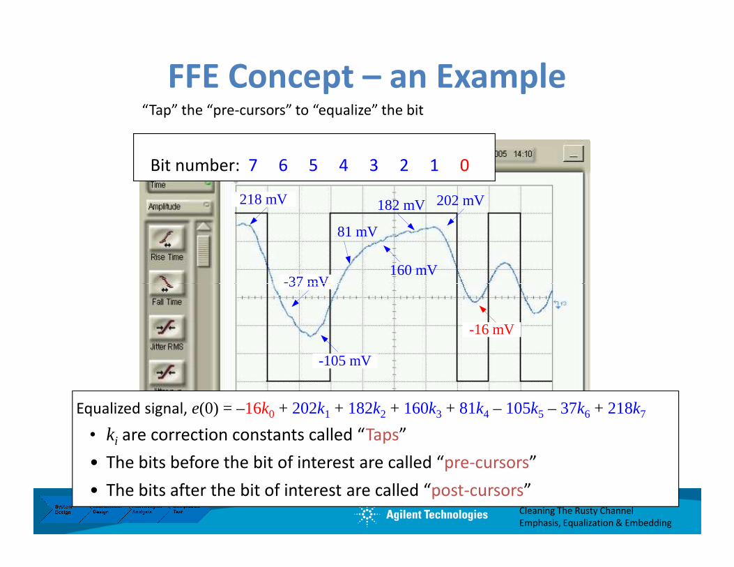
f(k) f(k) f(k) f(k) = = = = TapsTapsTapsTaps(k)(k)(k)(k) ⊗⊗⊗⊗ LP(bw) LP(bw) LP(bw) LP(bw) where LP is a 4where LP is a 4where LP is a 4where LP is a 4thththth order order order order Bessel.Bessel.Bessel.Bessel.
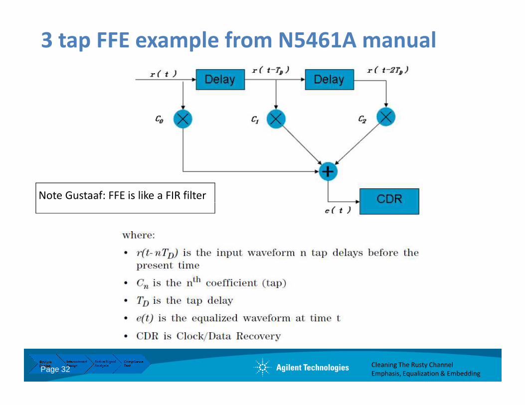
Tap values are dimensionless; they Tap values are dimensionless; they Tap values are dimensionless; they Tap values are dimensionless; they are a ratio of the voltage the are a ratio of the voltage the are a ratio of the voltage the are a ratio of the voltage the receiver should have seen to what it receiver should have seen to what it receiver should have seen to what it receiver should have seen to what it does see. does see. does see. does see. TapTapTapTap0000 is applied to the is applied to the is applied to the is applied to the current bit.current bit.current bit.current bit.
Decision
Circuit
Page 31
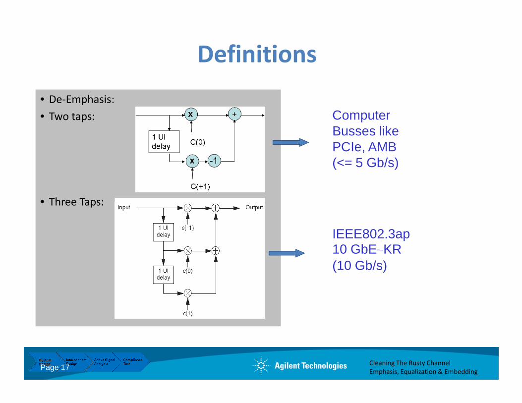
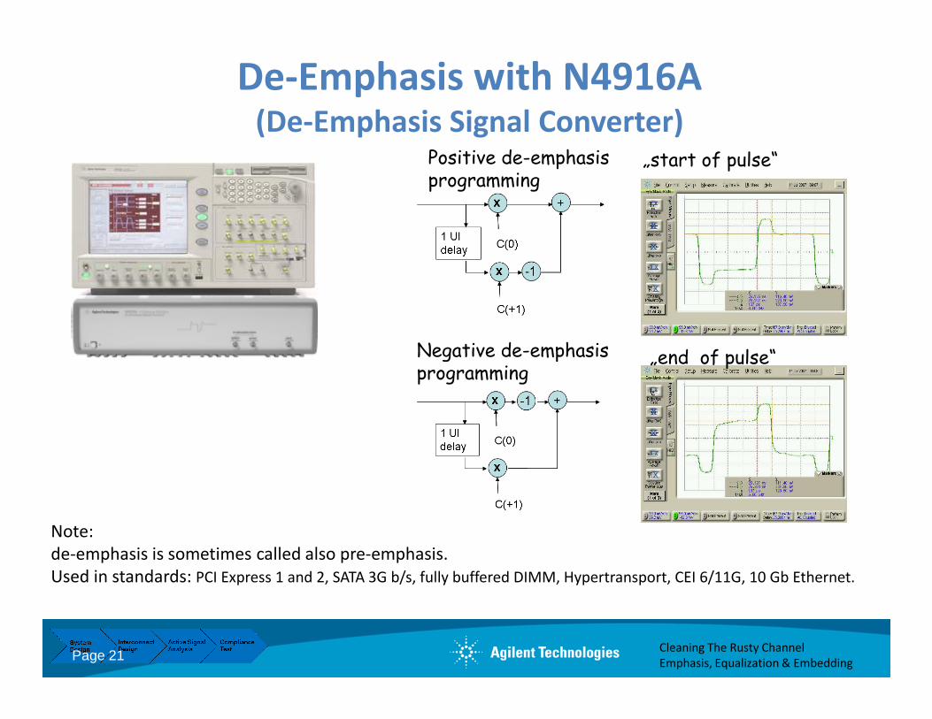
3 tap FFE example from N5461A manual
Note Gustaaf: FFE is like a FIR filter
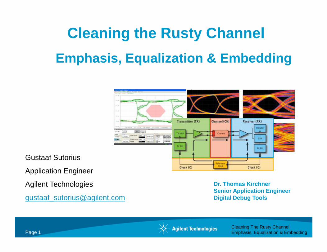
Cleaning The Rusty Channel
Emphasis, Equalization & Embedding Page 32
Basic Theory – Why Equalization Works
The Impulse Response h(t) has all the information contained in a circuit
element.
δ (t) h(t)
Transmission path
To get the best taps, we need to invert the process
h(t) e(t)
EqualizerDelay . . .Delay
++++
x x x x
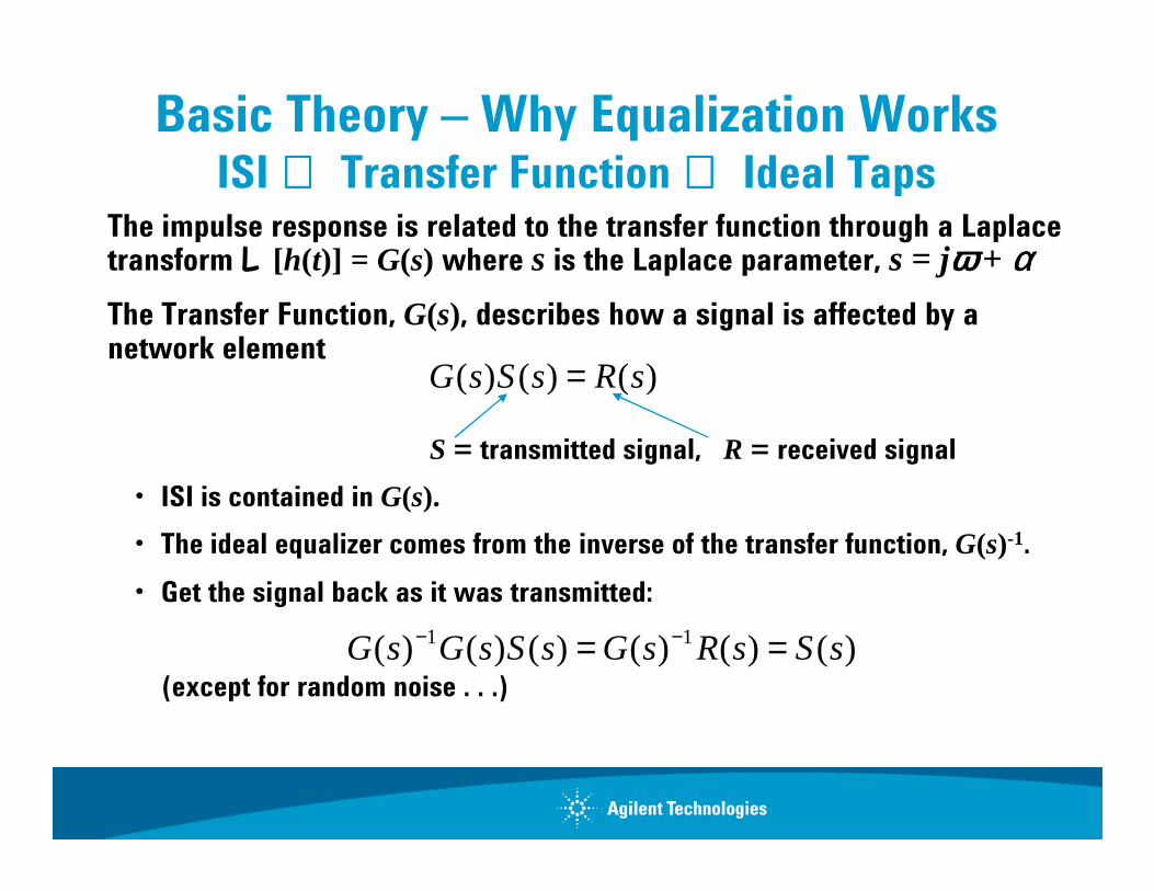
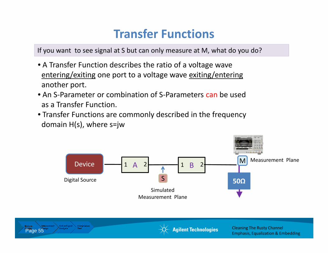
Basic Theory – Why Equalization Works ISI ⇔⇔⇔⇔ Transfer Function ⇔⇔⇔⇔ Ideal Taps
The impulse response is related to the transfer function through a Laplace transform L [h(t)] = G(s) where s is the Laplace parameter, s = jωωωω + ααααThe Transfer Function, G(s), describes how a signal is affected by a network element
S = transmitted signal, R = received signal
)()()( sRsSsG =
S = transmitted signal, R = received signal
• ISI is contained in G(s).
• The ideal equalizer comes from the inverse of the transfer function, G(s)-1.
• Get the signal back as it was transmitted:
(except for random noise . . .)
)()()()()()( 11 sSsRsGsSsGsG == −−
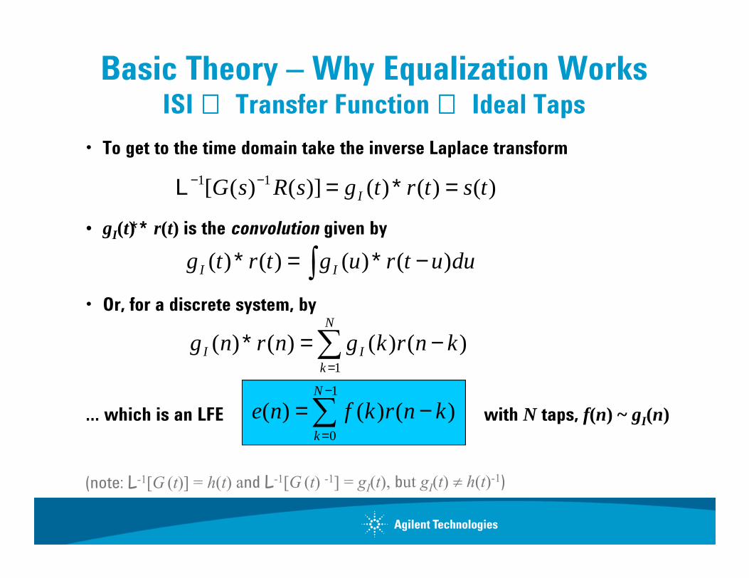
Basic Theory – Why Equalization Works ISI ⇔⇔⇔⇔ Transfer Function ⇔⇔⇔⇔ Ideal Taps
• To get to the time domain take the inverse Laplace transform
• gI(t) ∗ ∗ ∗ ∗ r(t) is the convolution given by
)()()()]()([ 11 tstrtgsRsG I =∗=−−L
∫ −∗=∗ duutrugtrtg II )()()()(
• Or, for a discrete system, by
… which is an LFE with N taps, f(n) ~ gI(n)∑−
=
−=1
0
)()()(N
k
knrkfne
∑=
−=∗N
kII knrkgnrng
1
)()()()(
Basic Theory – Why Equalization Works
Ideal vs actual LFE – MFB
The step from continuous, gI(t), to discrete, f(n) , makes a big difference
• The number of taps went from infinity to about 5 (which is << ∞∞∞∞)
The Matched Filter Bound (MFB) is the maximum possible signal to noise ratio when an equalizer exactly cancels ISI
Let h(i) be the impulse response of the channel, thenLet h(i) be the impulse response of the channel, then
∑ ∑∑−
=
−
=
∞
=
−+−−=1
0
1
00
)()()()()()(N
k
N
ki
knwkfiknsihkfne
The Decision Feedback Equalizer (DFE)
Start with an LFE and . . . fix it!
A perfect equalizer would remove all ISI,
leaving just the signal and the filtered noise
But an LFE:
1. Is discrete – usually one tap per bit, ISI is continuous.
∑−
=
−+=1
0
)()()()(N
k
knwkfnsne
1. Is discrete – usually one tap per bit, ISI is continuous.
2. Is finite – not long enough to completely correct the impulse
response.
3. Only uses information from the current and previous bits.
Introduce another correction based on the best guess of the current
and previous bits – a feedback term – to cancel the rest of the ISI
i.e., use the logic Decision to Feedback to the LFE output for better
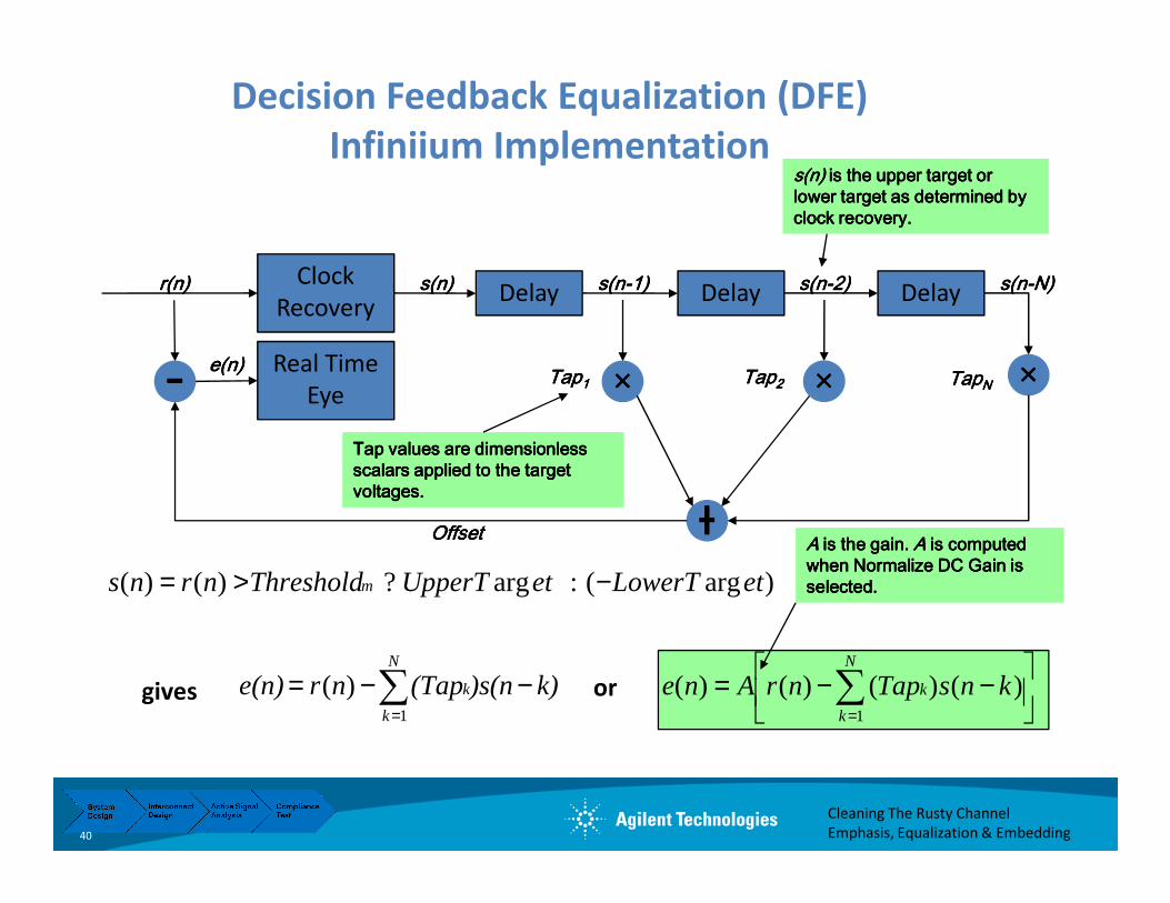
Tap values are dimensionless Tap values are dimensionless Tap values are dimensionless Tap values are dimensionless scalars applied to the +/scalars applied to the +/scalars applied to the +/scalars applied to the +/----
scalars applied to the +/scalars applied to the +/scalars applied to the +/scalars applied to the +/----amplitude voltages. amplitude voltages. amplitude voltages. amplitude voltages.
)(:?)()( AmplitudeAmplitudeThresholdnrns DC −>=
Page 38
• r(n) is the signal at the receiver.
• s(n) is the +/- amplitude as determined by
comparing the incoming signal is the given
Threshold.
• b(n) is the bit sequence coming out of the
receiver.
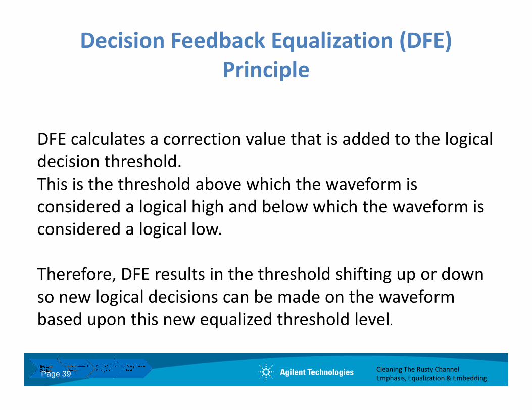
Decision Feedback Equalization (DFE)
Principle
DFE calculates a correction value that is added to the logical
decision threshold.
This is the threshold above which the waveform is
considered a logical high and below which the waveform is
Cleaning The Rusty Channel
Emphasis, Equalization & Embedding Page 39
considered a logical high and below which the waveform is
considered a logical low.
Therefore, DFE results in the threshold shifting up or down
so new logical decisions can be made on the waveform
TapTapTapTap1111 TapTapTapTapNNNNTapTapTapTap2222Real Time
Eye
s(n) s(n) s(n) s(n) is the upper target or is the upper target or is the upper target or is the upper target or lower target as determined by lower target as determined by lower target as determined by lower target as determined by clock recovery.clock recovery.clock recovery.clock recovery.
Tap values are dimensionless Tap values are dimensionless Tap values are dimensionless Tap values are dimensionless
r(n)r(n)r(n)r(n)
e(n)e(n)e(n)e(n)
Clock
Recovery
Cleaning The Rusty Channel
Emphasis, Equalization & Embedding
−−= ∑=
N
k
k knsTapnrAne1
)()()()(
∑=
−−=N
k
k k))s(n(Tapnre(n)1
)(gives or
OffsetOffsetOffsetOffset AAAA is the gain. is the gain. is the gain. is the gain. AAAA is computed is computed is computed is computed when Normalize DC Gain is when Normalize DC Gain is when Normalize DC Gain is when Normalize DC Gain is selected.selected.selected.selected.
Tap values are dimensionless Tap values are dimensionless Tap values are dimensionless Tap values are dimensionless scalars applied to the target scalars applied to the target scalars applied to the target scalars applied to the target voltages. voltages. voltages. voltages.
40
)arg(:arg?)()( etLowerTetUpperTThresholdnrns m −>=
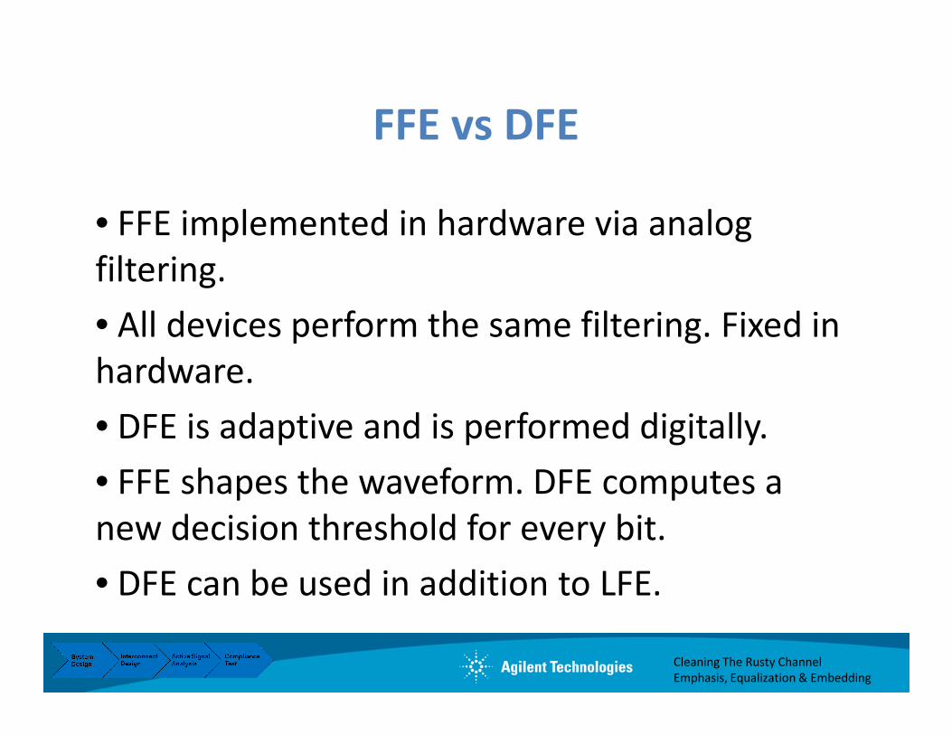
FFE vs DFE
• FFE implemented in hardware via analog
filtering.
• All devices perform the same filtering. Fixed in
hardware.
Cleaning The Rusty Channel
Emphasis, Equalization & Embedding
hardware.
• DFE is adaptive and is performed digitally.
• FFE shapes the waveform. DFE computes a
new decision threshold for every bit.
• DFE can be used in addition to LFE.
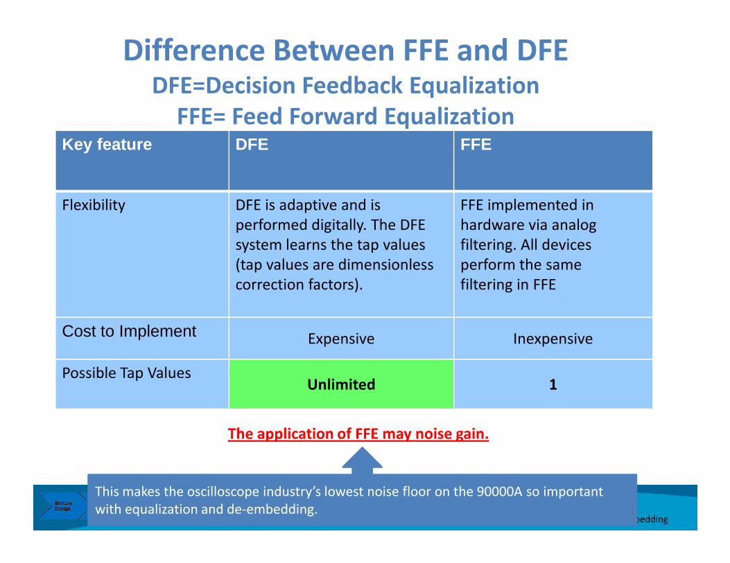
Difference Between FFE and DFEDFE=Decision Feedback Equalization
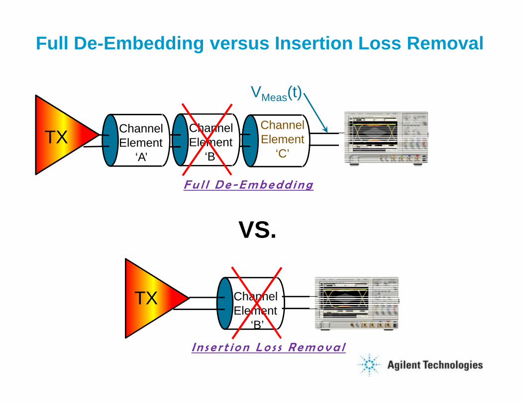
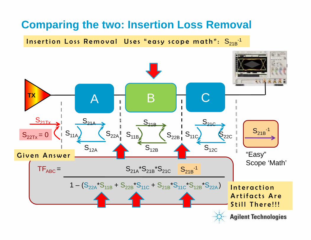
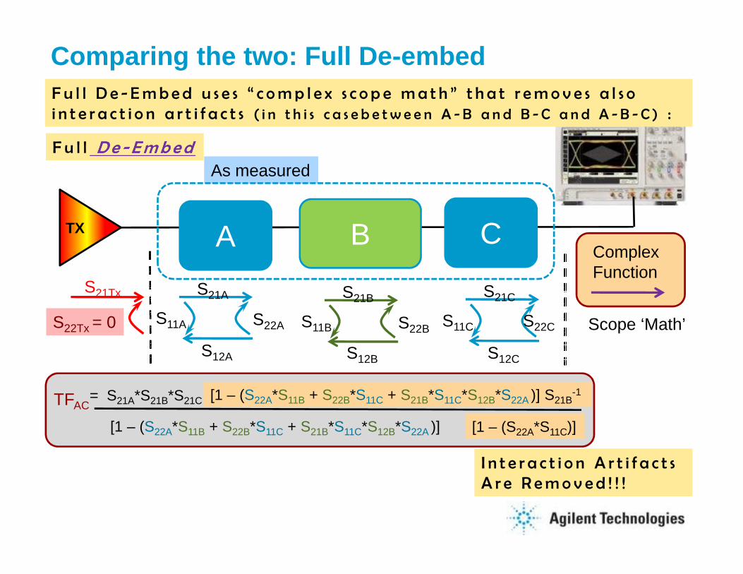
I n t e r a c t i o n A r t i f a c t s A r e S t i l l T h e r e ! ! !
S21B-1
“Easy” Scope ‘Math’
S21B-1
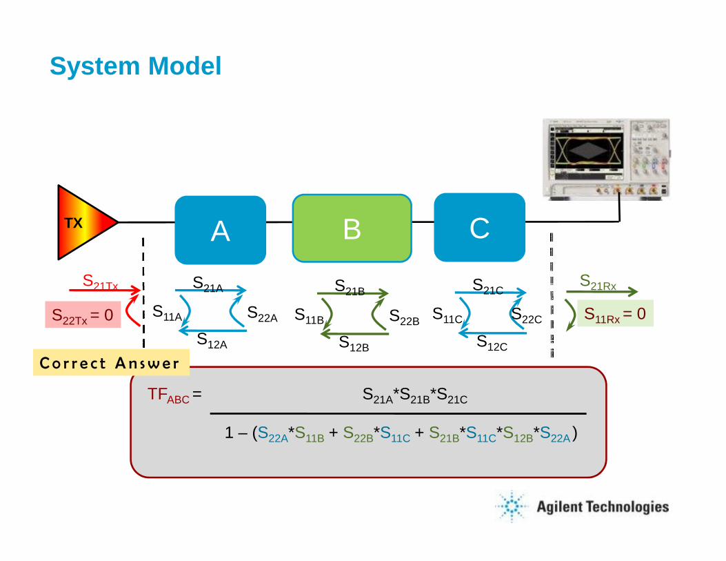
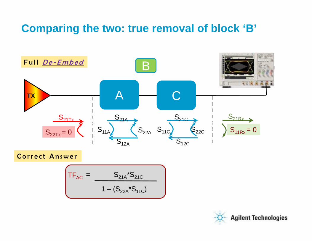
Comparing the two: true removal of block ‘B’
A
B
C
S21A S21C
TX
F u l l DeDe -- Emb edEmb ed
S21Tx S21RxS21A
S12A
S11A S22A
S21C
S12C
S11C S22C
TFAC
1 – (S22A*S11C)
= S21A*S21C
C o r r e c t A n sw e r
S21Tx
S22Tx = 0 S11Rx = 0
A B C
S S S
TX
S21Tx
F u l l DeDe -- Emb edEmb ed
Comparing the two: Full De-embed
As measured
Complex Function
F u l l D e - Emb ed u s e s “ c omp l e x s c o p e ma t h ” t h a t r emo v e s a l s o i n t e r a c t i o n a r t i f a c t s ( i n t h i s c a s e b e t w e e n A - B a n d B - C a n d A - B - C ) :
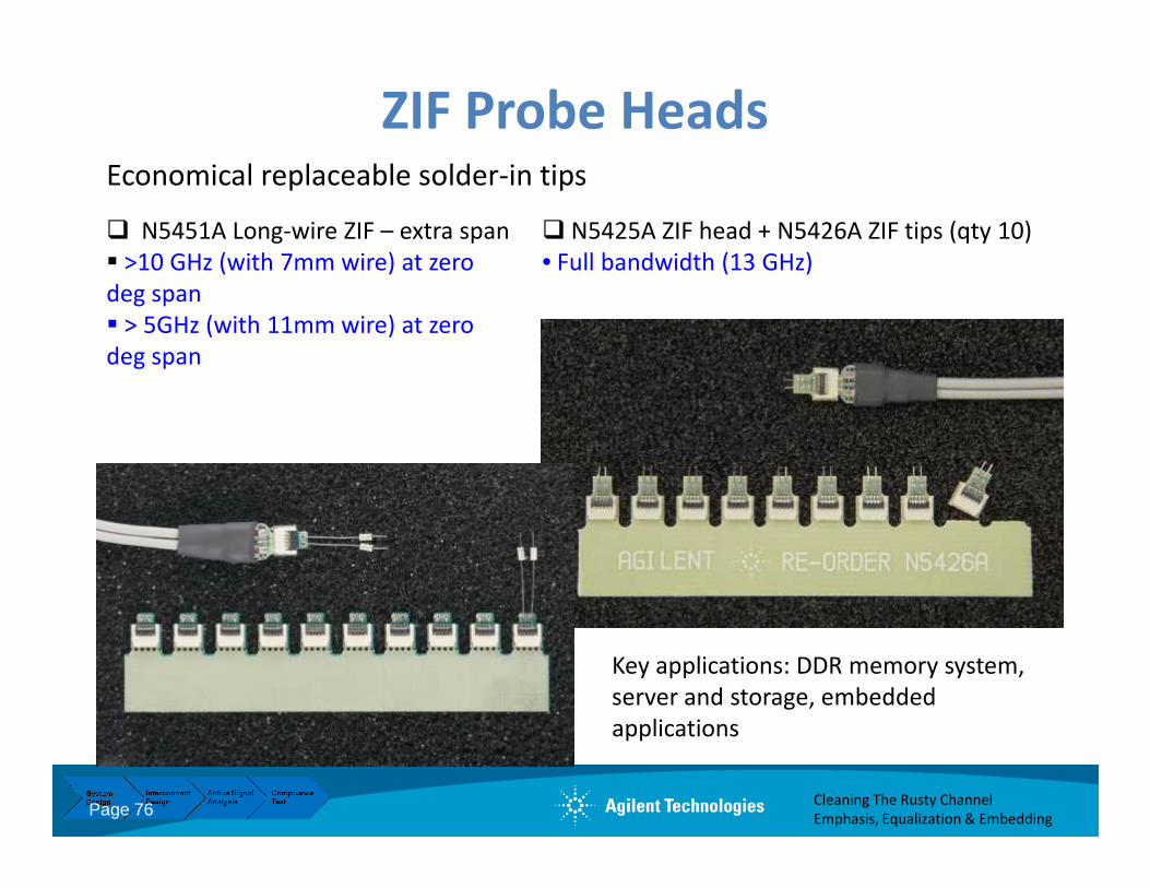
probe headprobe head8GHz SMA probe head8GHz SMA probe head
12GHz Socket 12GHz Socket
probe headprobe head
6GHz differential6GHz differentialbrowser probe headbrowser probe head
5GHz single end5GHz single endbrowser probe headbrowser probe head
1212--13GHz 13GHz differentialdifferentialsoldersolder--in probe in probe headhead
1212--13GHz 13GHz differentialdifferentialZIF solderZIF solder--in probe in probe head & ZIF Tip & head & ZIF Tip & Long Wire ZIF Tip Long Wire ZIF Tip (4~9GHz)(4~9GHz)
Page 77
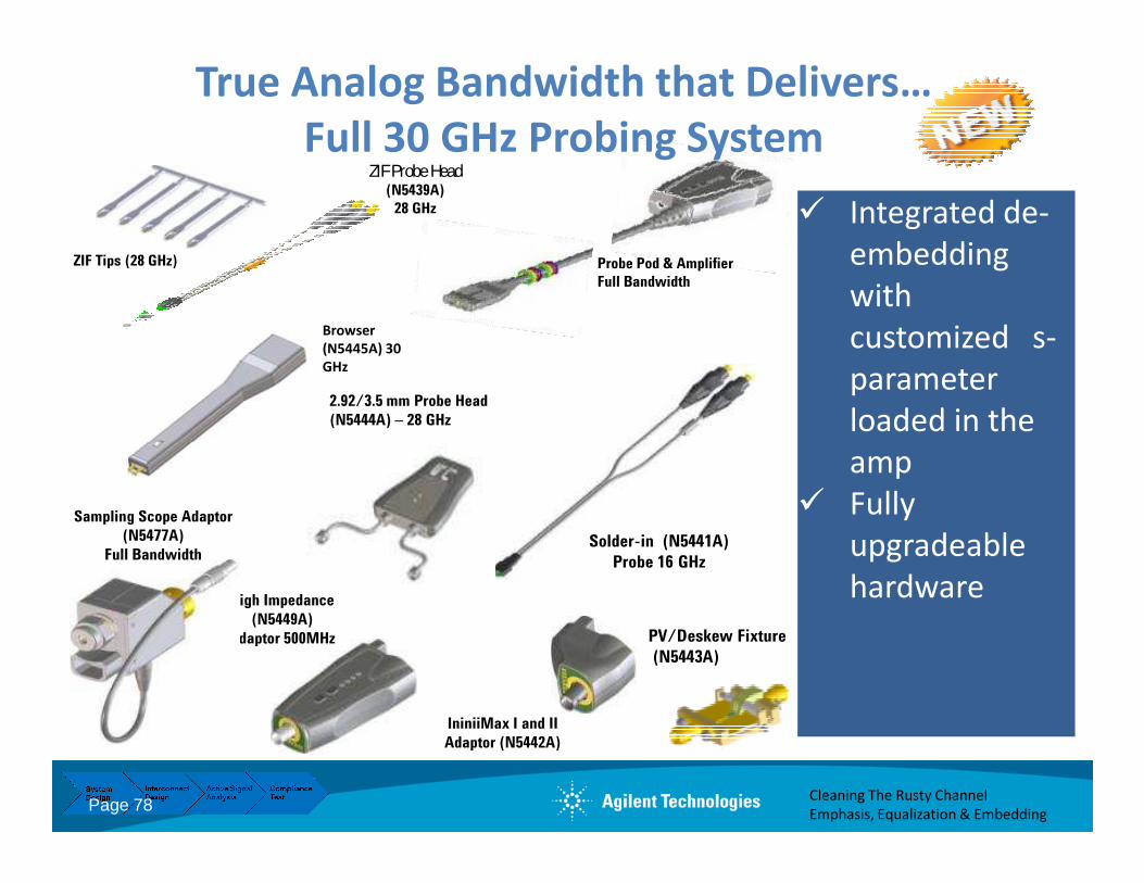
ZIF Probe Head (N5439A)
28 GHz
Probe Pod & Amplifier
Full Bandwidth
ZIF Tips (28 GHz)
2.92/3.5 mm Probe Head
(N5444A) – 28 GHz
Integrated de-
embedding
with
customized s-
parameter
loaded in the
amp
True Analog Bandwidth that Delivers…
Full 30 GHz Probing System
Browser
(N5445A) 30
GHz
Cleaning The Rusty Channel
Emphasis, Equalization & Embedding
Solder-in (N5441A)
Probe 16 GHz
PV/Deskew Fixture
(N5443A)
High Impedance
(N5449A)
Adaptor 500MHz
Sampling Scope Adaptor
(N5477A)
Full Bandwidth
IniniiMax I and II
Adaptor (N5442A)
amp
Fully
upgradeable
hardware
Page 78
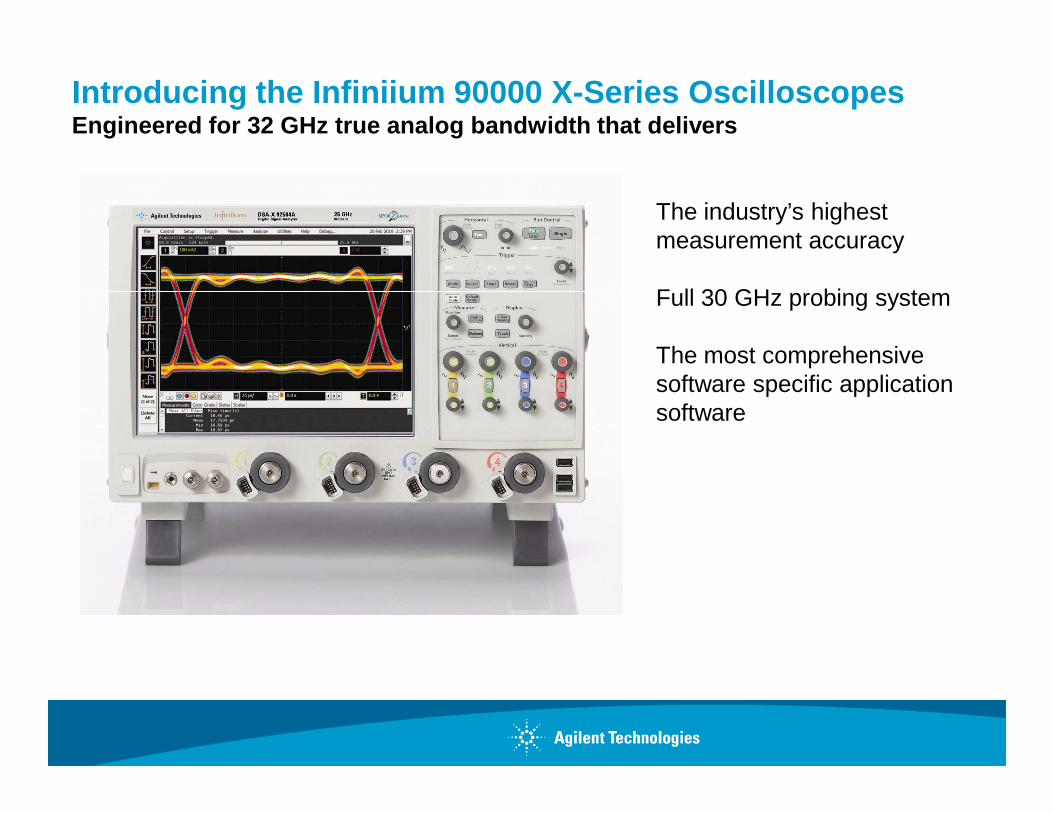
Introducing the Infiniium 90000 X-Series Oscillosco pesEngineered for 32 GHz true analog bandwidth that del ivers
The industry’s highest measurement accuracy
Full 30 GHz probing system
The most comprehensive software specific application software software
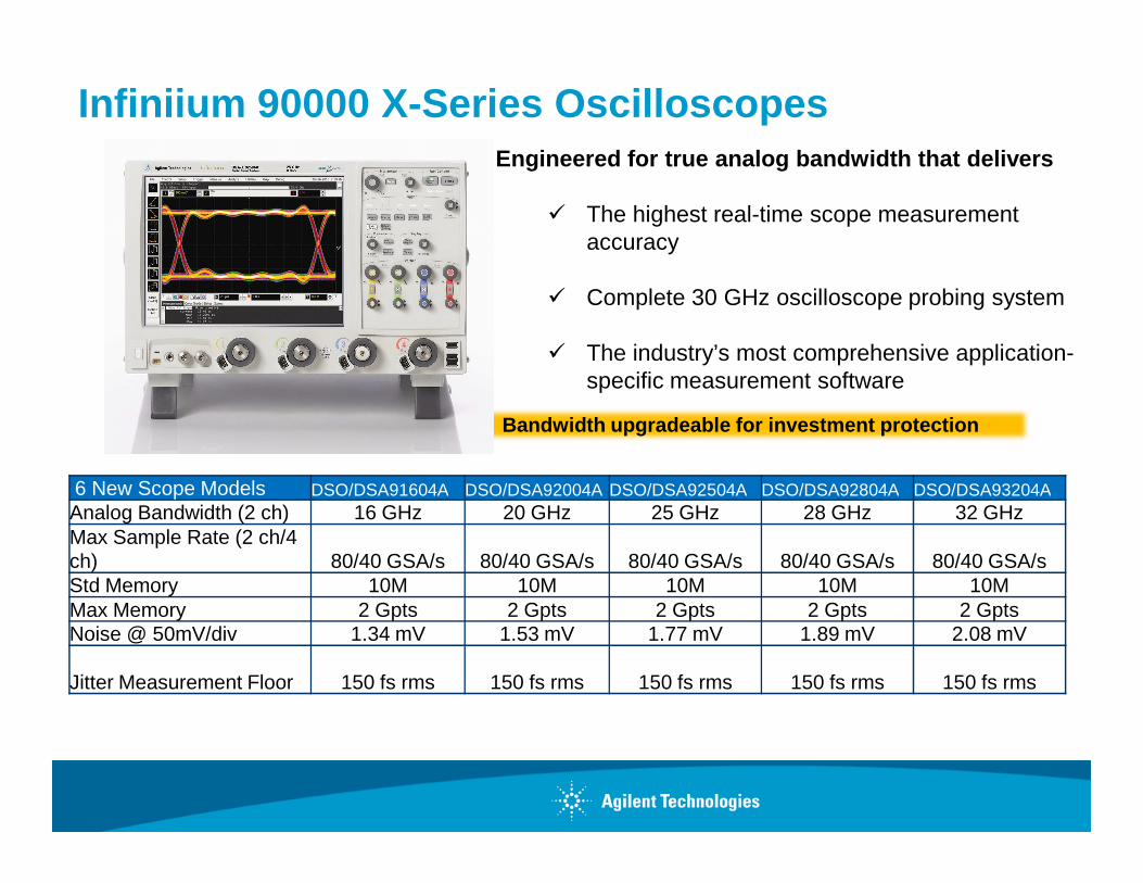
Infiniium 90000 X-Series OscilloscopesEngineered for true analog bandwidth that delivers
The highest real-time scope measurement accuracy
Complete 30 GHz oscilloscope probing system
The industry’s most comprehensive application-specific measurement software
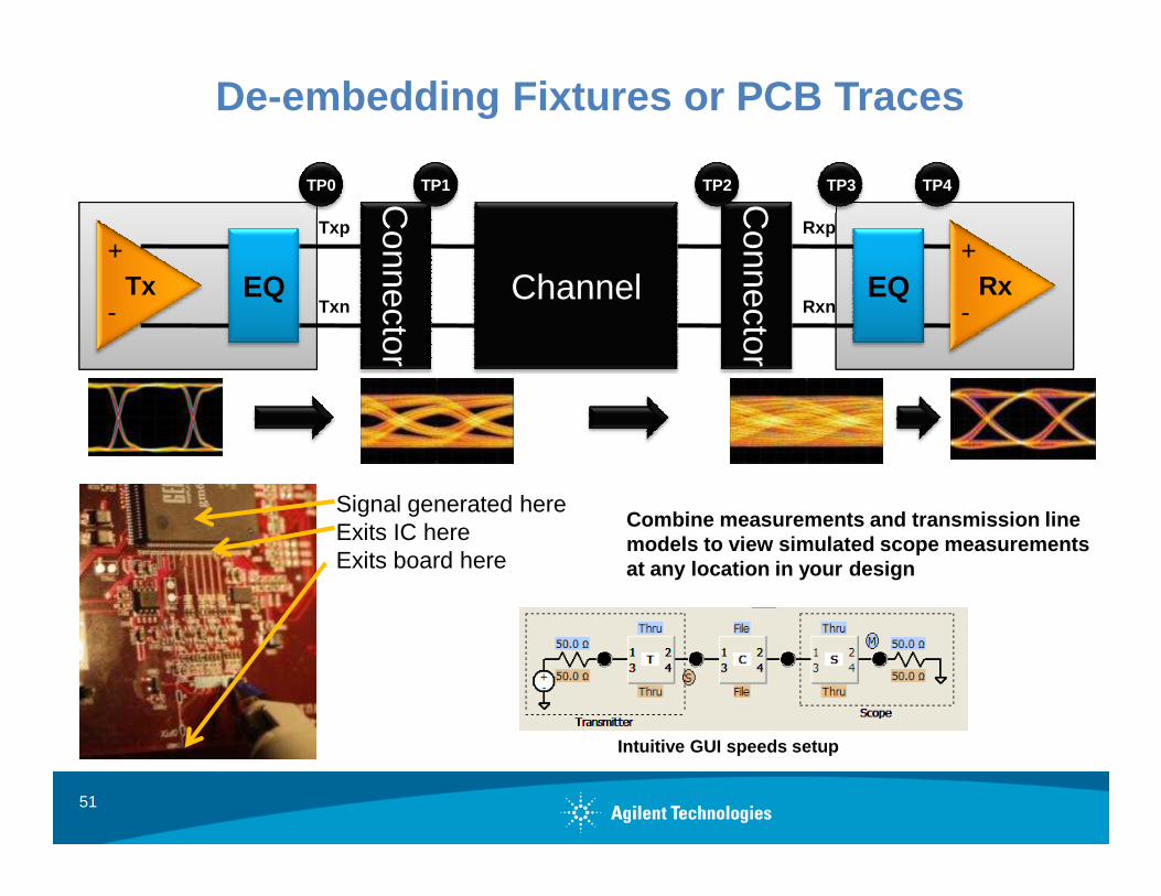
What parameters get measured? Full characterize includes measuring amplitude, rise/fall times, jitter (all types), etc. under various operating conditions.
IC - Top IC - Bottom
Device: ASIC / FPGA / SERDES / Other High-Speed IC
84
(all types), etc. under various operating conditions.
Who? Where? Performed by engineers and technicians in Performance Verification (PV) and Characterization labs
How are they measured?Accuracy and precision is critical, so engineers often use a sampling scope due to:
• High analog bandwidth (18GHz->90GHz)• Low noise (<300uV)• Ultra-low jitter (RJ<60fs)
Custom FixturesAccurate characterization often requires custom fixt ures.
• Probing introduces measurement challenges• Bring signals out to connectors• Good fixture layout minimizes signal degradation
DUTTX Output at the
Test FixtureMeasure actual signal here using cables between fixture and scope (connectorized)
A B
85
pads/balls of the IC
• Problem: Fixture will degrade signal and may not represent e nd-user’s implementation
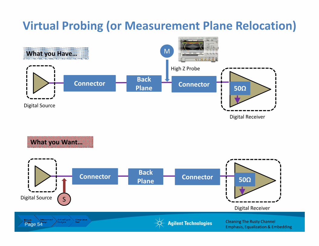
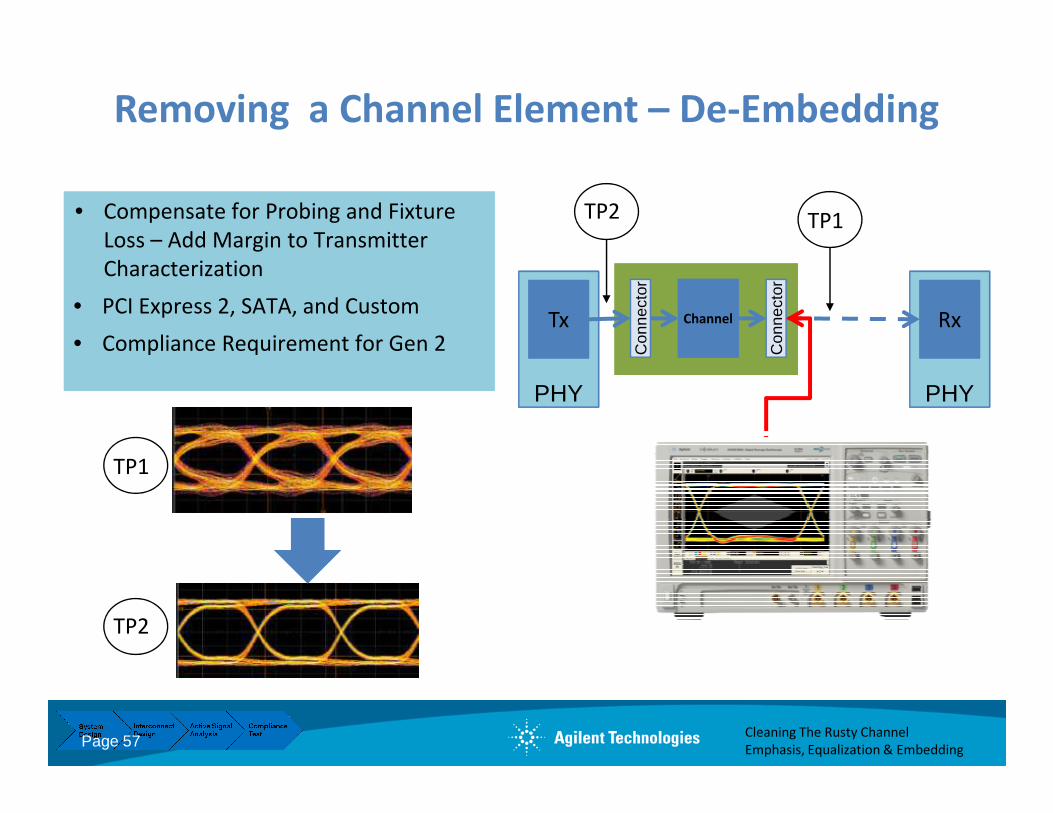
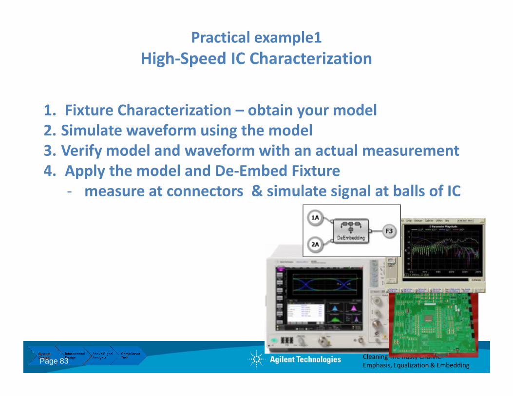
• Solution: Remove fixture effects of the transmission line fro m pt A to pt B (commonly referred to as de-embedding ). Allows us to predict the TX performance at the balls/pins of the IC, and/or predict performance using a differen t layout/material
Step 1: Fixture Characterization – obtain your mode l Generate an S-parameter model
a. Simulation o Use design software such as Agilent ADS, PLTS
b. Measure o Use VNA (ENA/PNA) or TDRo Do-It-Yourself or consult with an expert
such as GigaTest Labs
Characterize raw (unpopulated) board – plan ahead!• Add test coupons to fixture (e.g. Connector – pad, pad - Connector)• Layout pads with adjacent grounds for probing e.g. GSSG, GSGS, GSGGSG• Full S-Parameters - need differential probe that includes ground contacts
Differential Probe - usually used with positioner- select specific footprint,pitch, may be adjustable
ConnectorIC Pad
Goal: Accurately characterize the signal path from pad to connector.Generate a .s2p or .s4p Touchstone file.
AA
BB
N1021B
Step 2-3 Use your model to Simulate…then Verify
2. Simulate waveform using model (input –> apply S-parameter model -> output)
• simulate expected DUT TX signal (e.g. 10Gb/s, PRBS7, Rise/Fall Time = 25ps)
SW Simulated Input Signal
SW Simulated Output Signal
Embed Function
Simulated point A Simulated point B
87
3. Verify model and waveform with an actual measurement (inject signal from PG –> actual DUT -> measure O/P)
• generate expected DUT TX signal using BERT, inject via probe, measure on scope
Input Signal from PG Measured Output Signal
Probe DUT(raw board)
Simulated point B
Point A Measured point B
GoodCorrelation
Step 4 - Fixture Removal (de-embedding)
4. De-Embed Fixture- measure at connectors (B), simulate signal at balls of IC (A)
Pink = de -embedded signalYellow = measured signal
De-EmbeddedOutput Signal
Signal from DUT
88
Pink = de -embedded signalYellow = measured signal (Actual DUT + Fixture + Cables)
Benefits:• Improved Margins• More accurate representation of TXperformance (at point ‘A’)
• Simulate signal using different fixturewithout building it (cascade functions)• Gain valuable insightNote – could also remove cable effects too
AB
Measure at Point B Simulated Signal at Point A
Case Study – design your fixtures carefully!
DUT - fixtureSMA-pads
Characterize fixture with Agilent TDR and probe
S-Parameter has notch at 4.5GHz
Eye DiagramPurple – raw signal (reflection)Green – de-embedded signal (noise)
TDR into open (Step Response) has a very long settling time (triple transit)
Step 1
1a
1b
Steps 2, 3, 4a
Hi Z
Nio coupling
A B
probe-> Generate .s4p
notch at 4.5GHzGreen – de-embedded signal (noise)
Summary large notch in S-Parameter due to large reflection in the fixture (be wary of triple-transit !!) the ‘inverse’ function (de-embed) amplifies a lot of noise in the notch region => causes ringing must setup de-embed function to filter out notch at 4.5MHz. if left “as is”, max data rate for fixture ~1Gb/s. analyzing S-parameters can help predict effectiveness of de-embedding (look for excessive loss)
Step 4b5
89
SI design flaws cannot be hidden by De-emphasis, Equalization or de-embedding/virtual probing!!!!!
Agenda7. Practical Examples
1. High-Speed Characterization (effect of 4.5 GHz Notch in test fixture)
2. BGA probe setup in infiniisim Virtual Probe
3. Tuned, measurement enhanced, IBIS parameters for DDR DDR
4. Creating S2P (touchstone) files from Gerber files
5. Basic Steps for Optimizing a Serial Link
6. Serial Data Analysis Solutions: 8b10b Trigger, Decode, Search and Listing Feature
7. Small peek inside the 90.000 X 32 GHz scope
Page 90
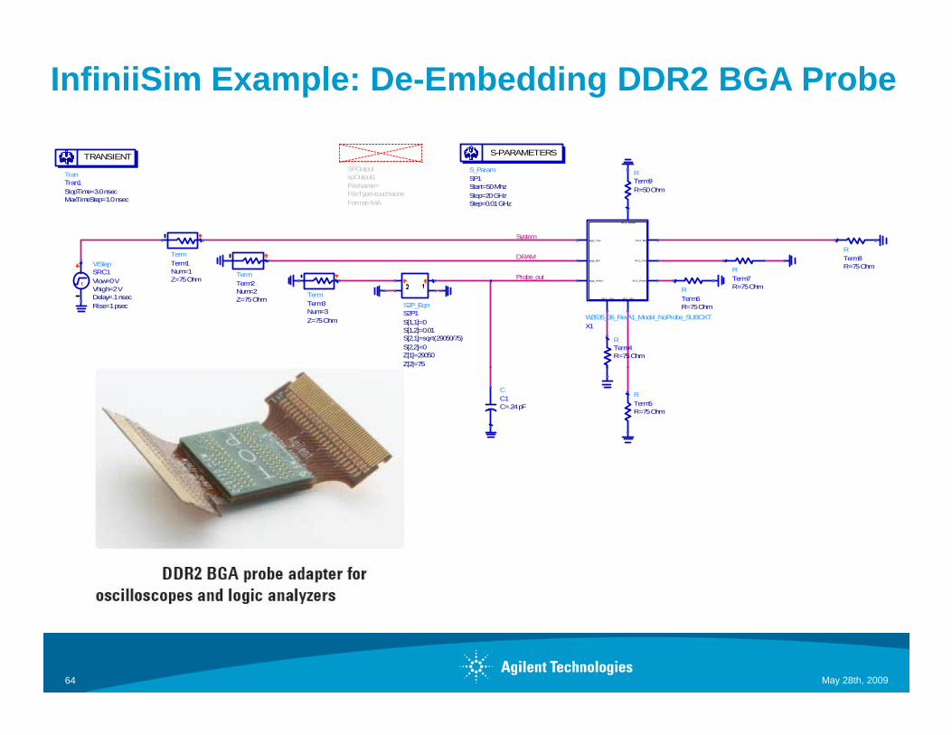
BGA BGA BGA BGA ProbeProbeProbeProbe PortPortPortPortMonitoring Pad = 1Monitoring Pad = 1Monitoring Pad = 1Monitoring Pad = 1Memory side =2Memory side =2Memory side =2Memory side =2 Board side = 3Board side = 3Board side = 3Board side = 3 internal branching point = 4 internal branching point = 4 internal branching point = 4 internal branching point = 4
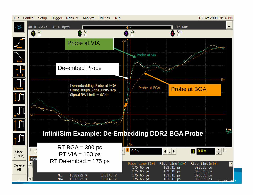
Observation point shift with Observation point shift with Observation point shift with Observation point shift with InfiniisimInfiniisimInfiniisimInfiniisim
Observation point shift with Observation point shift with Observation point shift with Observation point shift with InfiniisimInfiniisimInfiniisimInfiniisim
Infiniisim
We have only applied the channel S-parameters.
The delay is good, but the reflection and amplitude aren’t reproduced.
That means that it isn’t enough with the channel S-parameters only.
Observation point shift with Observation point shift with Observation point shift with Observation point shift with InfiniisimInfiniisimInfiniisimInfiniisim
Infiniisim
Package S-parameters
and Chip Die capacitance
The delay and the first edge are perfectly reproduced.
But the ripples on the plateau are wrong.
That means that the Infiniisim settings are still wrong or something is lacking.
That is you have to re-examine your simulation. => Let’s go to Example 3
July 21, 2010
Agenda 7. Practical Examples
1. High-Speed Characterization (effect of 4.5 GHz Notch in test fixture)
2. BGA probe setup in infiniisim Virtual Probe
3. Tuned, measurement enhanced, IBIS parameters for DDR
Cleaning The Rusty ChannelEmphasis, Equalization & Embedding
DDR
4. Creating S2P (touchstone) files from Gerber files
5. Basic Steps for Optimizing a Serial Link
6. Serial Data Analysis Solutions: 8b10b Trigger, Decode, Search and Listing Feature
7. Small peek inside the 90.000 X 32 GHz scope
Page 96
Practical example3
Simulation and Measurement Cooperation“connected solutions”
Cleaning The Rusty Channel
Emphasis, Equalization & Embedding Page 97
Simulation and Measurement Cooperation“connected solutions”
Oscilloscope
New Function:InfiniisimSimulation on the scope
Simulator (ADS)Simulation using measured waveform and S-parameters
Network Analyzer
New function:ENA-TDRSimulation on VNA
Agilent is the only one vendor delivering both simulation and measurement !
Simul and Meas, PCB board Straight Line
Straight line (test coupon).We have designed it to be Z=50 Ohm.
0.0
0.1
0.2
0.3
0.4
0.5
-0.1
0.6
Den
sity
2 4 6 8 10 12 14 16 180 20
-60
-50
-40
-30
-20
-10
-70
0
-6
-4
-2
-8
0
freq, GHz
dB(S
(1,1
))
dB(S
(2,1))
100 200 300 400 500 6000 700
time, psec
Simulated eye pattern and S-parameters at the design phase
100 200 300 400 500 6000 700
0.0
0.1
0.2
0.3
0.4
0.5
-0 .1
0.6
time , psec
Den
sity
Simulated Eye at the design phase
Measured Eye
Sim and Meas, PCB board Straight Line
Simulated S-parameters at the design phase
Measured Eye
Measured S-parameters
2 4 6 8 10 12 14 16 180 20
-30
-25
-20
-15
-10
-5
-35
0
-15
-10
-5
-20
0
freq, GHz
dB(S
(1,1
))
dB(S
(1,2))
dB(T
DR
_Tun
ing_
wS
MA
..S(1
,1)) dB
(TD
R_T
uning_wS
MA
..S(1,2))
Sim and Meas, PCB board Straight Line
Tune PCB board parameters so that the simulated and measuredS-parameters, TDR and TDT come very close.
er = 4.2
h= 360um
tanδ = 0.015
er = 4.5
h= 325um
tanδ = 0.023
Tuning Result
100 200 300 400 500 6000 700
0.0
0.1
0.2
0.3
0.4
0.5
-0.1
0.6
time, psec
Den
sity
Simulation before tuning
Sim and Meas, PCB board Straight Line
Simulation after tuning
Measured Eye
More complex channel
Simulation before tuning
Sim and Meas, PCB board Complex Channel
Use the same tuning as the test coupon(tuning parameters 2 slides back )
Simulated waveform at the DRAMSimulated waveform at the controller
Agenda 7. Practical Examples
1. High-Speed Characterization (effect of 4.5 GHz Notch in test fixture)
2. BGA probe setup in infiniisim Virtual Probe
3. Tuned, measurement enhanced, IBIS parameters for DDR
Cleaning The Rusty ChannelEmphasis, Equalization & Embedding
DDR
4. Creating S2P (touchstone) files from Gerber files
5. Basic Steps for Optimizing a Serial Link
6. Serial Data Analysis Solutions: 8b10b Trigger, Decode, Search and Listing Feature
7. Small peek inside the 90.000 X 32 GHz scope
Page 108
Practical example 4:Creating S2P files from Gerber files
1. Import Layout from mechanical CAD software into Genesys or ADS
2. Inspect layer stack and ensure material propertie s are correct
3. Insert EM Ports and Add Momentum Planar EM simulation controller
Page 109
simulation controller4. Run EM simulation and Graph Results5. Export Touchstone file to use in de-embedding net work
in Scope
Agilent Genesys : Cost Efficient, High Performance R F/MW Board Design Software
RF System Architecture
Circuit
Genesys Core Design Environment
Month ##, 200X
Circuit Syntheses Planar 3D EM Simulation
Frequency-domain Nonlinear
Time-domain
Nonlinear Frequency PlanningAntenna Far Field
Linear Sim& Data Display
GENESYS: An Advanced User Interface
A modern, integrated Windows environment
Easy-to-use - “Hard to forget”
Layouts Equations
TuneWindow
VendorModels
Page 111
Schematics
WorkspaceTree
Graphs& Tables
Window Models
STEP 1: Import Layout from mechanical CAD software into Genesys
Supported File Formats for import:
- DXF DWG- GDS II- Gerber
STEP 2: Inspect layer stack and ensure material properties are correct
Supported File Formats for import:
- DXF DWG- GDS II- Gerber
STEP 3: Insert EM Ports and Add Momentum Planar EM simulation controller
STEP 4: Run EM simulation and Graph Results
- - Layout with Momentum Mesh overlay
- Layout 3D View
-Graph of S-parameters
Very simple to setup for accurate results. All simulation options left to default (automatic)
STEP 5: Export Touchstone file to use in de-embedding network in Scope
Agenda 7. Practical Examples
1. High-Speed Characterization (effect of 4.5 GHz Notch in test fixture)
2. BGA probe setup in infiniisim Virtual Probe
3. Tuned, measurement enhanced, IBIS parameters for DDR
Cleaning The Rusty ChannelEmphasis, Equalization & Embedding
DDR
4. Creating S2P (touchstone) files from Gerber files
5. Basic Steps for Optimizing a Serial Link
6. Serial Data Analysis Solutions: 8b10b Trigger, Decode, Search and Listing Feature
7. Small peek inside the 90.000 X 32 GHz scope
Page 117
Practical example 5:Basic Steps for Optimizing a Serial Link
Page 118
Optimizing a Serial Link
PC BoardDSA9000 series & N5461A Equalization Analysis allows to analyze and optimize the signal integrity
Xilinx:
Multi-Gigabit Transceivers (MGTs)
+ IBERT Test Core
• IBERT core provides stimulus, • Tx & Rx setting control, and • BER measurement capability
Agilent:
Measurement instruments for analysis and optimization of signal integrity of Rocket IO signals
FPGA
IBERTIBERTIBERTIBERT
FPGA
PC Board
IBERTIBERTIBERTIBERTInsert core with
FPGA design SW
N4903B BERT and N4916B De-Emphasized Signal Converter allows to generate any pre-emphasis signal.
allows to analyze and optimize the signal integrity including automated tap optimizer for opening the eye. Graphical margin analysis via eye diagram measurements including mask templates allows to control optimization process.
Page 119
Optimizing Rocket IO Signal IntegrityBasic Steps for Optimizing a Serial Link:
1. Specify MGT configuration using Xilinx ISE tools, per your design’s characteristics.
2. Specify IBERT core parameters using Xilinx ChipScope Pro Core Generator consistent with #1 above; create IBERT core.
3. Load IBERT core and generate serial data .
4. Replace IBERT Tx by SerialBERT + De-Emphasized Sig nal Converter and optimize pre-emphasis controlled by BER
measurement in IBERT Rx or JBERT N4903B. Alternatively, the optimal pre-emphasis setting could be controlled by using the eye measurement in IBERT Rx or JBERT N4903B. Alternatively, the optimal pre-emphasis setting could be controlled by using the eye
opening measurement in the Realtime Scope 90000 series. The results of the optimization taps for Pre-emphasis could directly be
used in the Multi-Gigabit Transceivers (MGT) of Tx.
5. Replace IBERT Rx by Scope and determine the optim al tap values for equalizer in the Rx using automated tap finder routine in
the N5461A Equalization Software. The result of optimal equalization could be controlled by eye opening measurement in the
Realtime Scope 90000 series at Rx. The optimal settings for equalization taps could directly be used in the MGT of the Rx.
The weakness of the mask test is that violation points do not hold any time domain information. None will know when in the bit sequence it violated the mask. The Mask Unfold feature allow users to return to the exact eye violation location with time stamp info.
Serial Data Analysis Solutions Mask Unfold Feature
Ex: Ex: 1.51.5Gbps Serial ATA PRBSGbps Serial ATA PRBS