Features • Compliant to RoHS directives • 850 nm Vertical Cavity Surface Emitting Laser (VCSEL) • Class 1 eye safe per IEC60825-1 and CDRH • Wide temperature range (0 °C to 70 °C) • LC duplex connector optical interface conforming to ANSI TIA/EIA604-10 (FOCIS 10A) • Diagnostic features per SFF-8472 “Diagnostic Monitor- ing Interface for Optical Transceivers” • Enhanced operational features including EWRAP, OWRAP and variable electrical EQ/emphasis settings • Real time monitoring of: - Transmitter average optical power - Received average optical power - Laser bias current - Temperature - Supply Voltage • SFP+ mechanical specifications per SFF-8432 • SFP+ compliant low speed interface • Fibre Channel FC-PI-5 compliant high speed interface - 1600-SN-M6-S, 800-SN-M6-S, 400-SN-M6-I - 1600-SN-M5-S, 800-SN-M5-S, 400-SN-M5-I - 1600-SN-M5E-I, 800-SN-M5E-I, 400-SN-M5E-I - 1600-SN-M5F-I, 800-SN-M5F-I, 400-SN-M5F-I • Fibre Channel FC-PI-5 compliant optical link distances Applications • Fibre Channel switches (director, stand alone, blade) • Fibre Channel Host Bus Adapters • Fibre Channel RAID controllers • Fibre Channel tape drive • Port side connections • Inter-switch or inter-chassis aggregated links Description Avago Technologies’ AFBR-57F5MZ optical transceiver supports high speed serial links over multi-mode opti- cal fiber at signalling rates up to 14.025 Gb/s (the serial line rate of 16GFC). The product is compliant with Small Form Pluggable industry agreements SFP and SFP+ for mechanical and low speed electrical specifications. High speed electrical and optical specifications are compliant with ANSI Fibre Channel FC-PI-5. The AFBR-57F5MZ is a multi-rate 850nm transceiver which ensures compliance with FC-PI-5 16GFC, 8GFC and 4GFC specifications. Per the requirements of 16GFC, inter- nal clock and data recovery circuits (CDRs) are present on both electrical input and electrical output of this trans- ceiver. These CDRs will lock at 14.025 Gb/s (16GFC) but must be bypassed for operation at 8.5 Gb/s (8GFC) and 4.25 Gb/s (4GFC), accomplished by using two Rate Select inputs to configure transmit and receive sides. Transmitter and receiver can operate at different data rates, as is often seen during Fibre Channel speed negotiation. Digital diagnostic monitoring information (DMI) is present in the AFBR-57F5MZ per the requirements of SFF-8472, providing real time monitoring information of transceiver laser, receiver and environment conditions over a SFF- 8431 2-wire serial interface. AFBR-57F5MZ 16GFC SFP+ Digital Diagnostic SFP, 850 nm, 16G/8G/4G Low Voltage (3.3 V) Fibre Channel Optical Transceiver Data Sheet Related Products • AFBR-57D7APZ: 850 nm SFP for 8G/4G/2G Fibre Channel • AFCT-57D5ATPZ: 1310 nm SFP for 8G/4G/2G Fibre Channel • AFCT-57D5ANPZ: 1310 nm SFP for 8G/4G/2G Fibre Channel • AFBR-57R5APZ: 850 nm SFP for 4G/2G/1G Fibre Channel • AFCT-57R5APZ: 1310 nm SFP for 4G/2G/1G Fibre Channel • AFCT-57R5ATPZ: 1310 nm SFP for 4G/2G/1G Fibre Channel • AFCT-57R5ANPZ: 1310 nm SFP for 4G/2G/1G Fibre Channel Patent - www.avagotech.com/patents
Transcript
Features• Compliant to RoHS directives• 850 nm Vertical Cavity Surface Emitting Laser (VCSEL)• Class 1 eye safe per IEC60825-1 and CDRH• Wide temperature range (0 °C to 70 °C)• LC duplex connector optical interface conforming to
ANSI TIA/EIA604-10 (FOCIS 10A)• Diagnostic features per SFF-8472 “Diagnostic Monitor-
ing Interface for Optical Transceivers”• Enhanced operational features including EWRAP,
OWRAP and variable electrical EQ/emphasis settings• Real time monitoring of:
- Transmitter average optical power- Received average optical power- Laser bias current- Temperature- Supply Voltage
• SFP+ mechanical specifications per SFF-8432• SFP+ compliant low speed interface • Fibre Channel FC-PI-5 compliant high speed interface
• Fibre Channel FC-PI-5 compliant optical link distances
Applications• Fibre Channel switches (director, stand alone, blade)• Fibre Channel Host Bus Adapters• Fibre Channel RAID controllers• Fibre Channel tape drive• Port side connections• Inter-switch or inter-chassis aggregated links
DescriptionAvago Technologies’ AFBR-57F5MZ optical transceiver supports high speed serial links over multi-mode opti-cal fiber at signalling rates up to 14.025 Gb/s (the serial line rate of 16GFC). The product is compliant with Small Form Pluggable industry agreements SFP and SFP+ for mechanical and low speed electrical specifications. High speed electrical and optical specifications are compliant with ANSI Fibre Channel FC-PI-5.
The AFBR-57F5MZ is a multi-rate 850nm transceiver which ensures compliance with FC-PI-5 16GFC, 8GFC and 4GFC specifications. Per the requirements of 16GFC, inter-nal clock and data recovery circuits (CDRs) are present on both electrical input and electrical output of this trans-ceiver. These CDRs will lock at 14.025 Gb/s (16GFC) but must be bypassed for operation at 8.5 Gb/s (8GFC) and 4.25 Gb/s (4GFC), accomplished by using two Rate Select inputs to configure transmit and receive sides. Transmitter and receiver can operate at different data rates, as is often seen during Fibre Channel speed negotiation.
Digital diagnostic monitoring information (DMI) is present in the AFBR-57F5MZ per the requirements of SFF-8472, providing real time monitoring information of transceiver laser, receiver and environment conditions over a SFF-8431 2-wire serial interface.
AFBR-57F5MZ16GFC SFP+ Digital Diagnostic SFP, 850 nm, 16G/8G/4G Low Voltage (3.3 V) Fibre Channel Optical Transceiver
Data Sheet
Related Products• AFBR-57D7APZ: 850 nm SFP for 8G/4G/2G Fibre Channel
• AFCT-57D5ATPZ: 1310 nm SFP for 8G/4G/2G Fibre Channel
• AFCT-57D5ANPZ: 1310 nm SFP for 8G/4G/2G Fibre Channel
• AFBR-57R5APZ: 850 nm SFP for 4G/2G/1G Fibre Channel
• AFCT-57R5APZ: 1310 nm SFP for 4G/2G/1G Fibre Channel
• AFCT-57R5ATPZ: 1310 nm SFP for 4G/2G/1G Fibre Channel
• AFCT-57R5ANPZ: 1310 nm SFP for 4G/2G/1G Fibre Channel
Patent - www.avagotech.com/patents
2
InstallationThe AFBR-57F5MZ can be installed in any SFF-8074i com-pliant Small Form Pluggable (SFP) port regardless of host equipment operating status. The AFBR-57F5MZ is hot-pluggable, allowing the module to be installed while the host system is operating and on-line. Upon insertion, the transceiver housing makes initial contact with the host board SFP cage, mitigating potential damage due to Elec-tro-Static Discharge (ESD).
Digital Diagnostic Interface and Serial IdentificationThe 2-wire serial interface is based on ATMEL AT24C01A series EEPROM protocol and signaling detail. Conven-tional EEPROM memory, bytes 0-255 at memory address 0xA0, is organized in compliance with SFF-8074i. New digital diag nostic information, bytes 0-255 at memory ad-dress 0xA2, is compliant to SFF-8472. The new diagnostic information provides the opportunity for Predictive Fail-ure Identification, Com pliance Prediction, Fault Isolation and Component Monitoring.
Predictive Failure IdentificationThe AFBR-57F5MZ predictive failure feature allows a host to identify potential link problems before system perfor-mance is impacted. Prior identification of link problems enables a host to service an application via “fail over” to a redundant link or replace a suspect device, maintaining system uptime in the process. For applications where ul-tra-high system uptime is required, a digital SFP provides a means to monitor two real-time laser metrics asso ciated with observing laser degradation and predicting failure: average laser bias current (Tx_Bias) and average laser op-tical power (Tx_Power).
Compliance Prediction Compliance prediction is the ability to determine if an optical transceiver is operating within its operating and environmental requirements. AFBR-57F5MZ devices pro-vide real-time access to transceiver internal supply volt-age and temperature, allowing a host to identify potential component compliance issues. Received optical power is also available to assess compliance of a cable plant and remote transmitter. When operating out of requirements, the link cannot guarantee error free transmission.
Fault IsolationThe fault isolation feature allows a host to quickly pin-point the location of a link failure, minimizing downtime. For optical links, the ability to identify a fault at a local de-vice, remote device or cable plant is crucial to speeding service of an installation. AFBR-57F5MZ real-time moni-tors of Tx_Bias, Tx_Power, Vcc, Temperature and Rx_Power can be used to assess local transceiver current operating conditions. In addition, status flags Tx_Disable and Rx Loss of Signal (LOS) are mirrored in memory and available via the two-wire serial interface.
Component MonitoringComponent evaluation is a more casual use of the AFBR-57F5MZ real-time monitors of Tx_Bias, Tx_Power, Vcc, Temperature and Rx_Power. Potential uses are as debug-ging aids for system installation and design, and transceiv-er parametric evaluation for factory or field qualification. For example, temperature per module can be observed in high density applications to facilitate thermal evaluation of blades, PCI cards and systems.
3
Figure 1. Transceiver functional diagram.
Rx Vout &Emphasis
RxCDR
TxEqualization
TxCDR
LIGHT FROM FIBER
LIGHT TO FIBER
PHOTO-DETECTOR
RECEIVER
AMPLIFICATION& QUANTIZATION
RD+ (RECEIVE DATA)
RD- (RECEIVE DATA)
Rx LOSS OF SIGNAL
VCSEL
TRANSMITTER
LASERDRIVER &
SAFETYCIRCUITRY
TX_DISABLE
TD+ (TRANSMIT DATA)
TD- (TRANSMIT DATA)
TX_FAULT
ELECTRICAL INTERFACE
MOD-DEF2 (SDA)
MOD-DEF1 (SCL)
MOD-DEF0
µController
OPTICAL INTERFACE
Rx RATE SELECT RS(0)
Tx RATE SELECT RS(1)
tween successive assertions of this control signal. Tx_Dis-able can also be asserted via the two-wire serial interface (address A2h, byte 110, bit 6) and monitored (address A2h, byte 110, bit 7).
The contents of A2h, byte 110, bit 6 are logic OR’d with hardware Tx_Disable (pin 3) to control transmitter opera-tion.
Transmit Fault (Tx_Fault)A catastrophic laser fault will activate the transmitter sig-nal, TX_FAULT, and disable the laser. This signal is an open collector output (pull-up required on the host board). A low signal indicates normal laser operation and a high signal indicates a fault. The TX_FAULT will be latched high when a laser fault occurs and is cleared by toggling the TX_DISABLE input or power cycling the transceiver. The transmitter fault condition can also be monitored via the two-wire serial interface (address A2, byte 110, bit 2).
Eye Safety CircuitThe AFBR-57F5MZ provides Class 1 (single fault tolerant) eye safety by design and has been tested for compliance with the requirements listed in Table 1. The eye safety circuit continuously monitors the optical output power level and will disable the transmitter upon detecting an unsafe condition beyond the scope of Class 1 certification. Such unsafe conditions can be due to inputs from the host board (Vcc fluctuation, unbalanced code) or a fault within the transceiver.
Transmitter SectionThe transmitter section includes a Transmitter Optical SubAssembly (TOSA), laser driver circuit, Clock and Data Recovery circuit (CDR) and an electrical input stage with variable equalization controls and electrical eye mea-surement capability. The TOSA contains a 850 nm Vertical Cavity Surface Emitting Laser (VCSEL) light source with integral light monitoring function and imaging optics to assure efficient optical coupling to the LC connector in-terface. The TOSA is driven by a laser driver IC, which uses the differential output from an integral Tx CDR stage to modulate and regulate VCSEL optical power. As mandated by FC-PI-5, the integral CDR cleans up any incoming jit-ter accumulated from the host ASIC, PCB traces and SFP electrical connector. Between the SFP electrical connector and Tx CDR is a variable, I2C-bus controlled, equalization circuit to optimize SFP performance with non-ideal in-coming electrical waveforms. Note the Tx CDR is engaged only with Tx_RATE=high (16GFC) and bypassed with Tx_RATE=low (8G/4G).
Transmit Disable (Tx_Disable)The AFBR-57F5MZ accepts a TTL and CMOS compatible transmit disable control signal input (pin 3) which shuts down the transmitter optical output. A high signal im-plements this function while a low signal allows normal transceiver operation. In the event of a fault (e.g. eye safe-ty circuit activated), cycling this control signal resets the module as depicted in Figure 4. An internal pull up resistor disables the transceiver transmitter until the host pulls the input low. Host systems should allow a 10 ms interval be-
4
Receiver SectionThe receiver section includes a Receiver Optical SubAs-sembly (ROSA), pre-amplification and post-amplification circuit, Clock and Data Recovery Circuit and an electrical output stage with variable emphasis controls. The ROSA, containing a high speed PIN detector, pre-amplifier and imaging optics efficiently couple light from the LC con-nector interface and perform an optical to electrical con-version. The resulting differential electrical signal passes through a post amplification circuit and into a Clock and Data Recovery circuit (CDR) for cleaning up accumulated jitter. The resulting signal is passed to a high speed output line driver stage with variable, I2C-bus controlled, empha-sis settings allowing the host to optimize signal character-istics between the SFP and host ASIC. Note the Rx CDR is engaged only with Rx_RATE=high (16GFC) and bypassed with Rx_RATE=low (8G/4G).
Receiver Loss of Signal (Rx_LOS)The post-amplification IC also includes transition detec-tion circuitry which monitors the ac level of incoming op-tical signals and provides a TTL/CMOS compatible status signal to the host (pin 8). An adequate optical input results in a low Rx_LOS output while a high Rx_LOS output in-dicates an unusable optical input. The Rx_LOS thresholds are factory set so that a high output indicates a definite optical fault has occurred. Rx_LOS can also be monitored via the two-wire serial interface (address A2h, byte 110, bit 1).
Functional Data I/OThe AFBR-57F5MZ interfaces with the host circuit board through twenty I/O pins (SFP electrical connector) identi-fied by function in Table 2. The board layout for this inter-face is depicted in Figure 6.
The AFBR-57F5MZ high speed transmit and receive inter-faces require SFP MSA compliant signal lines on the host board. To simplify board requirements, biasing resistors and ac coupling capacitors are incorporated into the SFP transceiver module (per SFF-8074i) and hence are not re-quired on the host board. The Tx_Disable, Tx_Fault, and Rx_LOS lines require TTL lines on the host board (per SFF-8074i) if used. If an application chooses not to take advan-tage of the functionality of these pins, care must be taken to ground Tx_Disable (for normal operation).
Figure 2 depicts the recom mended interface circuit to link the AFBR-57F5MZ to supporting physical layer ICs. Tim-ing for MSA compliant control signals implemented in the transceiver are listed in Figure 4.
Application SupportAn Evaluation Kit and Reference Designs are available to assist in evaluation of the AFBR-57F5MZ. Please contact your local Field Sales representative for availability and ordering details.
CautionThere are no user serviceable parts nor maintenance re-quirements for the AFBR-57F5MZ. All mechanical adjust-ments are made at the factory prior to shipment. Tamper-ing with, modifying, misusing or improperly handling the AFBR-57F5MZ will void the product warranty. It may also result in improper operation and possibly overstress the laser source. Performance degrada tion or device failure may result. Connection of the AFBR-57F5MZ to a light source not compliant with ANSI FC-PI specifications, oper-ating above maximum operating conditions or in a man-ner inconsistent with it’s design and function may result in exposure to hazardous light radiation and may constitute an act of modifying or manufacturing a laser product. Per-sons performing such an act are required by law to re-cer-tify and re-identify the laser product under the provisions of U.S. 21 CFR (Subchapter J) and TUV.
Ordering InformationPlease contact your local field sales engineer or one of Avago Technologies franchised distributors for ordering information. For technical information, please visit Avago Technologies’ WEB page at www.avagotech.com or contact Avago Technologies Semiconductor Products Customer Response Center at 1-800-235-0312. For information re-lated to SFF Committee documentation visit www.sffcom-mittee.org.
Regulatory ComplianceThe AFBR-57F5MZ complies with all applicable laws and regulations as detailed in Table 1. Certification level is de-pendent on the overall configuration of the host equip-ment. The transceiver performance is offered as a figure of merit to assist the designer.
5
Electromagnetic Interference (EMI)Equipment incorporating gigabit transceivers is typically subject to regulation by the FCC in the United States, CENELEC EN55022 (CISPR 22) in Europe and VCCI in Japan. The AFBR-57F5MZ’s compliance to these standards is de-tailed in Table 1. The metal housing and shielded design of the AFBR-57F5MZ minimizes the EMI challenge facing the equipment designer.
EMI Immunity (Susceptibility)Due to its shielded design, the EMI immunity of the AFBR-57F5MZ exceeds typical industry standards.
FlammabilityThe AFBR-57F5MZ optical transceiver is made of metal and high strength, heat resistant, chemical resistant and UL 94V-0 flame retardant plastic.
Electrostatic Discharge (ESD)The AFBR-57F5MZ is compatible with ESD levels found in typical manufacturing and operating environments as de-scribed in Table 1. In the normal handling and operation of optical transceivers, ESD is of concern in two circum-stances.
The first case is during handling of the transceiver prior to insertion into an SFP compliant cage. To protect the de-vice, it’s important to use normal ESD handling pre-cau-tions. These include use of grounded wrist straps, work-benches and floor wherever a transceiver is handled.
The second case to consider is static discharges to the exterior of the host equipment chassis after installation. If the optical interface is exposed to the exterior of host equipment cabinet, the transceiver may be subject to sys-tem level ESD requirements.
Table 1. Regulatory Compliance Feature Test Method Performance Electrostatic Discharge (ESD) MIL-STD-883C Class 1 (> 2000 Volts) to the Electrical Pins Method 3015.4
Electrostatic Discharge (ESD) Variation of IEC 61000-4-2 Typically, no damage occurs with 25 kV when to the Duplex LC Receptacle the duplex LC connector receptacle is contacted by a Human Body Model probe.
GR1089 10 contacts of 8 kV on the electrical faceplate with device inserted into a panel.
Electrostatic Discharge (ESD) Variation of IEC 801-2 Air discharge of 15 kV (min.) contact to to the Optical Connector connector without damage.
Electromagnetic Interference FCC Class B System margins are dependent on customer (EMI) CENELEC EN55022 Class B board and chassis design. (CISPR 22A) VCCI Class 1
Immunity Variation of IEC 61000-4-3 Typically shows no measurable effect from a 10 V/m field swept from 10 MHz to 1 GHz.
Laser Eye Safety and US FDA CDRH AEL Class 1 CDRH certification 9720151-111 Equipment Type Testing US21 CFR, Subchapter J per TUV file 72102056 Paragraphs 1002.10 and 1002.12 (IEC) EN60825-1: 1994 + A11 + A2 (IEC) EN60825-2: 1994 + A1 (IEC) EN60950: 1992 + A1 + A2 + A3 + A4 + A11
Component Recognition Underwriters Laboratories and UL file 8543036783 Canadian Standards Association Joint Component Recognition for Information Technology Equipment including Electrical Business Equipment
RoHS Compliance Less than 1000 ppm of cadmium, lead, mercury, hexavalent chromium, polybrominated biphenyls, and polybrominated biphenyl ethers.
BAUARTGEPRUFT
TYPEAPPROVED
TUVRheinland
Product Safety
¬
¬
6
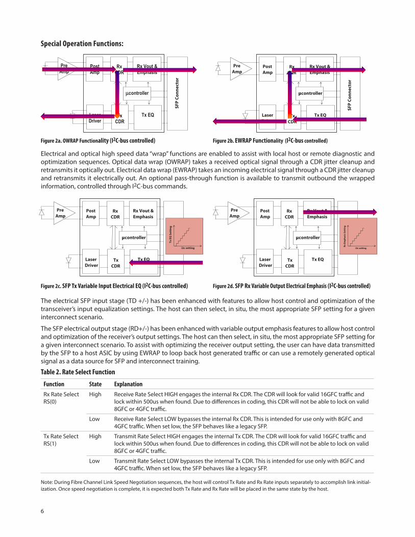
Special Operation Functions:
Electrical and optical high speed data “wrap” functions are enabled to assist with local host or remote diagnostic and optimization sequences. Optical data wrap (OWRAP) takes a received optical signal through a CDR jitter cleanup and retransmits it optically out. Electrical data wrap (EWRAP) takes an incoming electrical signal through a CDR jitter cleanup and retransmits it electrically out. An optional pass-through function is available to transmit outbound the wrapped information, controlled through I2C-bus commands.
The electrical SFP input stage (TD +/-) has been enhanced with features to allow host control and optimization of the transceiver’s input equalization settings. The host can then select, in situ, the most appropriate SFP setting for a given interconnect scenario.
The SFP electrical output stage (RD+/-) has been enhanced with variable output emphasis features to allow host control and optimization of the receiver’s output settings. The host can then select, in situ, the most appropriate SFP setting for a given interconnect scenario. To assist with optimizing the receiver output setting, the user can have data transmitted by the SFP to a host ASIC by using EWRAP to loop back host generated traffic or can use a remotely generated optical signal as a data source for SFP and interconnect training.
Table 2. Rate Select Function
Function State ExplanationRx Rate SelectRS(0)
High Receive Rate Select HIGH engages the internal Rx CDR. The CDR will look for valid 16GFC traffic and lock within 500us when found. Due to differences in coding, this CDR will not be able to lock on valid 8GFC or 4GFC traffic.
Low Receive Rate Select LOW bypasses the internal Rx CDR. This is intended for use only with 8GFC and 4GFC traffic. When set low, the SFP behaves like a legacy SFP.
Tx Rate SelectRS(1)
High Transmit Rate Select HIGH engages the internal Tx CDR. The CDR will look for valid 16GFC traffic and lock within 500us when found. Due to differences in coding, this CDR will not be able to lock on valid 8GFC or 4GFC traffic.
Low Transmit Rate Select LOW bypasses the internal Tx CDR. This is intended for use only with 8GFC and 4GFC traffic. When set low, the SFP behaves like a legacy SFP.
Note: During Fibre Channel Link Speed Negotiation sequences, the host will control Tx Rate and Rx Rate inputs separately to accomplish link initial-ization. Once speed negotiation is complete, it is expected both Tx Rate and Rx Rate will be placed in the same state by the host.
NOTE: INDUCTORS MUST HAVE LESS THAN 1Ω SERIES RESISTANCE TO LIMIT VOLTAGE DROP TO THE SFP MODULE.
22 µF
8
Notes:1. TX_FAULT is an open collector/drain output, which must be pulled up with a 4.7 k – 10 kΩ resistor on the host board. When high, this output indi-
cates a laser fault of some kind. Low indicates normal operation. In the low state, the output will be pulled to < 0.8 V.2. TX_DISABLE is an input that is used to shut down the transmitter optical output. It is internally pulled up (within the transceiver) with a 6.8 kΩ
resistor. Low (0 – 0.8 V): Transmitter on Between (0.8 V and 2.0 V): Undefined High (2.0 – Vcc max) or OPEN: Transmitter Disabled3. The signals Mod-Def 0, 1, 2 designate the two wire serial interface pins. They must be pulled up with a 4.7 k – 10 kΩ resistor on the host board. Mod-Def 0 is grounded by the module to indicate the module is present Mod-Def 1 is serial clock line (SCL) of two wire serial interface Mod-Def 2 is serial data line (SDA) of two wire serial interface 4. RX_LOS (Rx Loss of Signal) is an open collector/drain output that must be pulled up with a 4.7 k – 10 kΩ resistor on the host board. When high, this
output indicates the received optical power is below the worst case receiver sensitivity (as defined by the standard in use). Low indicates normal operation. In the low state, the output will be pulled to < 0.8 V.
5. RD-/+ designate the differential receiver outputs. They are AC coupled 100 Ω differential lines which should be terminated with 100 Ω differential at the host SERDES input. AC coupling is done inside the transceiver and is not required on the host board. The voltage swing on these lines will be between 370 and 850 mV differential (185 – 425 mV single ended) when properly terminated.
6. VccR and VccT are the receiver and transmitter power supplies. They are defined at the SFP connector pin. The maximum supply current is 300 mA and the associated in-rush current will typically be no more than 30 mA above steady state after 2 microseconds.
7. TD-/+ designate the differential transmitter inputs. They are AC coupled differential lines with 100 Ω differential termination inside the module. The AC coupling is done inside the module and is not required on the host board. The inputs will accept differential swings of 180 – 1200 mV (90 – 600 mV single ended)
8. Rate_Select is an input that is used to control transmit and receive high speed parametric optimizaton. It is internally pulled down (within the transceiver) with a 40kOhm resistor. Low (0 - 0.8V) or Open: Rate is set to 8.5Gb/s and below optimization. The CDR is bypassed. Between (0.8V and 2.0V) Undefined High (2.0 - Vcc max): Rate is set to 14.025Gb/s optimization. The CDR is engaged.
Table 3. Pin DescriptionPin Name Function/Description Notes
1 VeeT Transmitter Ground
2 TX_FAULT Transmitter Fault Indication – High indicates a fault condition Note 1
3 TX_DISABLE Transmitter Disable – Module electrical input disables on high or open Note 2
4 MOD-DEF2 Module Definition 2 – Two wire serial ID interface data line (SDA) Note 3
5 MOD-DEF1 Module Definition 1 – Two wire serial ID interface clock line (SCL) Note 3
Notes;1. Absolute Maximum Ratings are those values beyond which damage to the device may occur if these limits are exceeded for other than a short
period of time. See Reliability Data Sheet for specific reliability performance.2. Between Absolute Maximum Ratings and the Recommended Operating Conditions functional performance is not intended, device reliability is
not implied, and damage to the device may occur over an extended period of time.3. The module supply voltages, VCCT and VCCR must not differ by more than 0.5 V or damage to the device may occur.
Table 5. Recommended Operating Conditions
Parameter Symbol Minimum Maximum Unit Notes
Case Operating Temperature TC 0 70 °C Note 1, 2
Supply Voltage VccT, R 3.135 3.465 V Note 2
Data Rate 4.25 14.025 Gb/s Note 2
Notes:1. The Ambient Operating Temperature limitations are based on the Case Operating Temperature limitations and are subject to the host system
thermal design.2. Recommended Operating Conditions are those values for which functional performance and device reliability is implied.
Table 6. Transceiver Electrical Characteristics (TC = 0 °C to 70 °C, VccT, VccR = 3.3 V ± 5%)
Parameter Symbol Minimum Typical Maximum Unit Notes
AC Electrical Characteristics
Power Supply Noise Rejection (peak-peak) PSNR 100 mV Note 1
DC Electrical Characteristics
Module Supply Current ICC 300 mA
Low Speed Outputs: VOH 2.0 VccT,R+0.3 V Note 2
Transmit Fault (TX_FAULT), Loss of Signal VOL 0.8 V (RX_LOS), MOD-DEF 2
Low Speed Inputs: VIH 2.0 Vcc V Note 3
Transmit Disable (TX_DIS), MOD-DEF 1, VIL 0 0.8 V MOD-DEF2, RS(0), RS(1)
Notes:1. Filter per SFP specification is required on host board to remove 10 Hz to 2 MHz content.2. Pulled up externally with a 4.7 k – 10 kΩ resistor on the host board to 3.3 V.3. Mod-Def1 and Mod-Def2 must be pulled up externally with a 4.7 k – 10 kΩ resistor on the host board to 3.3 V.
10
Table 7. Transmitter and Receiver Electrical Characteristics(TC = 0 °C to 70 °C, VccT, VccR = 3.3 V ± 5%)
Parameter Symbol Min Typ Max Unit NotesHigh Speed Data InputTransmitter Differential Input Voltage (TD+/-)
VI 180 1200 mV Note 1
High Speed Data OutputReceiver Differential Output Voltage (RD+/-)
Vo 370 850 mV Note 2
Receiver Total Jitter (14.025 Gb/s) TJ 0.36 UI Note 3, Rx_Rate = high
Receiver Data Dependent Pulse Width Shrinkage (14.025 Gb/s)
DDPWS 0.14 UI Note 3, Rx_Rate = high
Receiver Data Dependent Pulse Width Shrinkage (8.5 Gb/s)
DDPWS 0.36 UI Note 4, Rx_Rate = low
Notes: 1. Internally ac coupled and terminated (100Ω differential).2. Internally ac coupled but requires an external load termination (100Ω differential).3. CDR is engaged with Rx_Rate = high. Received output jitter for 14.025 Gb/s.4. CDR is not engaged with Rx_Rate = low (ie. Bypassed). Receiver output jitter for 8.5 Gb/s and 4.25Gb/s.
Table 8. Transmitter Optical Characteristics(TC = 0 °C to 70 °C, VccT, VccR = 3.3 V ± 5%)
Parameter Symbol Min Typ Max Unit NotesModulated Optical Output Power (OMA) (Peak to Peak) 14.025Gb/s
Tx,OMA 331 µW
Modulated Optical Output Power (OMA) (Peak to Peak) 8.5Gb/s
Tx,OMA 302 µW
Modulated Optical Output Power (OMA) (Peak to Peak) 4.25Gb/s
Tx,OMA 247 µW
Average Optical Output Power Pout -7.8 dBm Note 1
Center Wavelength lc 840 860 nm
Spectral Width – rms qrms 0.59 nm
Optical Rise Time (20%-80%) tr, tf 30 ps
RIN12 (OMA) RIN -128 dB/Hz
Vertical Eye Closure Penalty, 14.025Gb/s VECP 2.56 dB Note 2
Transmitter Waveform Distortion Penalty, 8.5Gb/s TWDP 4.3 dB Note 3
Notes:1. Max Pout is the lesser of Class 1 safety limits (CDRH and EN 60825) or received power, max. 2. CDR is engaged with Tx_Rate = high. Transmitter output jitter for 14.025 Gb/s.3. CDR is not engaged with Tx_Rate = low (ie. Bypassed). Transmitter output jitter for 8.5 Gb/s and 4.25 Gb/s.
11
Table 9. Receiver Optical and Electrical Characteristics(TC = 0 °C to 70 °C, VccT, VccR = 3.3 V ± 5%)
Parameter Symbol Min Typ Max Unit NotesOptical Input Power PIN 0 dBm,avg
Input Optical Modulation Amplitude, 14.025Gb/s(Peak to Peak) [Unstressed Sensitivity]
OMA 89 µW,OMA Note 1
Input Optical Modulation Amplitude, 8.5Gb/s(Peak to Peak) [Unstressed Sensitivity]
OMA 76 µW,OMA Note 1
Input Optical Modulation Amplitude, 4.25Gb/s(Peak to Peak) [Unstressed Sensitivity]
Notes:1. Input Optical Modulation Amplitude (commonly known as sensitivity] requires a valid Fibre Channel encoded input.2. 14.025 Gb/s stressed received vertical eye closure penalty (ISI) min is 2.5 dB for all fiber types.3. 8.5 Gb/s stressed received vertical eye closure penalty (ISI) min is 3.1 dB for all fiber types.4. 4.25 Gb/s stressed received vertical eye closure penalty (ISI) min is 0.75 dB for OM3 fiber, 1.67 dB for OM2 fiber and 2.14 dB for OM1 fiber..
12
Table 10. Transceiver SOFT DIAGNOSTIC Timing Characteristics (TC = 0 °C to 70 °C, VccT, VccR = 3.3 V ± 5%)
Parameter Symbol Minimum Maximum Unit Notes
Hardware TX_DISABLE Assert Time t_off 10 µs Note 1
Hardware TX_DISABLE Negate Time t_on 1 ms Note 2
Time to initialize, including reset of TX_FAULT t_init 300 ms Note 3
Hardware TX_FAULT Assert Time t_fault 100 µs Note 4
Hardware TX_DISABLE to Reset t_reset 10 µs Note 5
Hardware RX_LOS Deassert Time t_loss_on 100 µs Note 6
Hardware RX_LOS Assert Time t_loss_off 100 µs Note 7
Hardware RATE_SELECT Assert Time t_rate_high 1 ms Note 17
Hardware RATE_SELECT Deassert Time t_rate_low 1 ms Note 17
Software TX_DISABLE Assert Time t_off_soft 100 ms Note 8
Software TX_DISABLE Negate Time t_on_soft 100 ms Note 9
Software Tx_FAULT Assert Time t_fault_soft 100 ms Note 10
Software Rx_LOS Assert Time t_loss_on_soft 100 ms Note 11
Software Rx_LOS Deassert Time t_loss_off_soft 100 ms Note 12
Software Rate_Select Assert Time t_rate_on_soft 100 ms Note 18
Software Rate_Select Deassert Time t_rate_off_soft 100 ms Note 19
Analog parameter data ready t_data 1000 ms Note 13
Serial bus hardware ready t_serial 300 ms Note 14
Serial bus buffer time t_buf 20 µs Note 16
Write Cycle Time t_write 40 ms Note 15
Serial ID Clock Rate f_serial_clock 400 kHz
Notes: 1. Time from rising edge of TX_DISABLE to when the optical output falls below 10% of nominal. 2. Time from falling edge of TX_DISABLE to when the modulated optical output rises above 90% of nominal. 3. Time from power on or falling edge of Tx_Disable to when the modulated optical output rises above 90% of nominal. 4. From power on or negation of TX_FAULT using TX_DISABLE. 5. Time TX_DISABLE must be held high to reset the laser fault shutdown circuitry. 6. Time from loss of optical signal to Rx_LOS Assertion. 7. Time from valid optical signal to Rx_LOS De-Assertion. 8. Time from two-wire interface assertion of TX_DISABLE (A2h, byte 110, bit 6) to when the optical output falls below 10% of nominal. Measured
from falling clock edge after stop bit of write transaction. 9. Time from two-wire interface de-assertion of TX_DISABLE (A2h, byte 110, bit 6) to when the modulated optical output rises above 90% of nomi-
nal.10. Time from fault to two-wire interface TX_FAULT (A2h, byte 110, bit 2) asserted.11. Time for two-wire interface assertion of Rx_LOS (A2h, byte 110, bit 1) from loss of optical signal.12. Time for two-wire interface de-assertion of Rx_LOS (A2h, byte 110, bit 1) from presence of valid optical signal.13. From power on to data ready bit asserted (A2h, byte 110, bit 0). Data ready indicates analog monitoring circuitry is functional.14. Time from power on until module is ready for data transmission over the serial bus (reads or writes over A0h and A2h).15. Time from stop bit to completion of a 1 – 4 byte write command. Write cycle time is 80 ms max. for a 5 – 8 byte write.16. Time between STOP and START commands.17. Time from rising or falling edge of Rate_Select input until transceiver is successfully passing traffic as designated by RS(0) and RS(1). For Rate_
Select going high, the internal CDR will lock on valid 64b/66b encoded 14.025 Gb/s data within the specified time. For Rate_Select going low, the internal CDR will be bypassed within the specified time for transmission of valid 8b/10b encoded 8.5 Gb/s or 4.25 Gb/s data.
18. Time from two-wire interface Assertion of Rate_Select (either RS(0) in A2h, byte 110, bit 3 or RS(1) in A2h, byte 118, bit 3) to when the respective CDR is engaged at 14.025 Gb/s data rate.
19. Time from two-wire interface Deassertion of Rate_Select (either RS(0) in A2h, byte 110, bit 3 or RS(1) in A2h, byte 118, bit 3) to when the respec-tive CDR is bypassed for low speed 8.5 Gb/s or 4.25 Gb/s operation.
13
Figure 5. Transceiver timing diagrams (module installed except where noted)
TX_FAULT
OCCURANCE OF FAULT
t_fault
TX_DISABLE
TRANSMITTED SIGNAL
TX_FAULT
OCCURANCE OF FAULT
TX_DISABLE
TRANSMITTED SIGNAL
t-fault: TX FAULT ASSERTED, TX SIGNAL NOT RECOVERED t-reset: TX DISABLE ASSERTED THEN NEGATED, TX SIGNAL RECOVERED
t_resett_init** SFP SHALL CLEAR TX_FAULT IN
< t_init IF THE FAILURE IS TRANSIENT
TX_FAULT
OCCURANCE OF FAULT
t_fault
TX_DISABLE
TRANSMITTED SIGNAL
OPTICAL SIGNAL
LOS
t-fault: TX DISABLE ASSERTED THEN NEGATED, TX SIGNAL NOT RECOVERED t-loss-on & t-loss-off
t_loss_ont_init*
t_reset* SFP SHALL CLEAR TX_FAULT IN < t_init IF THE FAILURE IS TRANSIENT
t-init: TX DISABLE NEGATED, MODULE HOT PLUGGED t-off & t-on: TX DISABLE ASSERTED THEN NEGATED
INSERTION
t_on
Table 11. Transceiver Digital Diagnostic Monitor (Real Time Sense) Characteristics (TC = 0 °C to 70 °C, VccT, VccR = 3.3 V ± 5%)
Parameter Symbol Min. Units Notes Transceiver Internal Temperature TINT ±3.0 °C Temperature is measured internal to the transceiver. Accuracy Valid from = 0 °C to 70 °C case temperature.
Transceiver Internal Supply VINT ±0.1 V Supply voltage is measured internal to the transceiver Voltage Accuracy and can, with less accuracy, be correlated to voltage at the SFP Vcc pin. Valid over 3.3 V ± 10%.
Transmitter Laser DC Bias Current IINT ±10 % IINT is better than ±10% of the nominal value. Accuracy
Transmitted Average Optical PT ±3.0 dB Coupled into 50/125 µm multi-mode fiber. Valid from Output Power Accuracy 100 µW to 500 µW, avg.
Received Average Optical Input PR ±3.0 dB Coupled from 50/125 µm multi-mode fiber. Valid from Power Accuracy 31 µW to 500 µW, avg.
14
Table 12. EEPROM Serial ID Memory Contents – Address A0h
3 00 40 41 “A” - Vendor Name ASCII Character4 00 41 46 “F” - Vendor Name ASCII Character5 00 42 42 “B” - Vendor Name ASCII Character6 00 43 52 “R” - Vendor Name ASCII Character7 60 Short and Intermediate link distance (per FC-PI-5) 44 2D “-” - Vendor Name ASCII Character8 40 Shortwave laser without OFC (open fiber control) 45 35 “5” - Vendor Name ASCII Character9 0C Multi-mode 50 µm and 62.5 µm and optical media 46 37 “7” - Vendor Name ASCII Character
10 70 400, 800 and 1600 MByte/s FC-PI-5 speed [1] 47 46 “F” - Vendor Name ASCII Character11 06 64B/66B data at 14.025G & 8B/10B at 8.5G/4.25G 48 35 “5” - Vendor Name ASCII Character12 8C 14.025 Mbit/s nominal bit rate (14.025 Gb/s) 49 4D “M” - Vendor Name ASCII Character13 0A 16/8/4G Independent Tx and Rx Rate Selects 50 5A “Z” - Vendor Name ASCII Character14 00 51 20 “ ” - Vendor Name ASCII Character15 00 52 20 “ ” - Vendor Name ASCII Character16 04 35m of OM2 50/125um fiber at 14.025 Gb/s [2] 53 20 “ ” - Vendor Name ASCII Character17 02 15m of OM1 62.5/125um fiber at 14.025 Gb/s [3] 54 20 “ ” - Vendor Name ASCII Character18 00 55 20 “ ” - Vendor Name ASCII Character19 0A 100m of OM3 50/125um fiber at 14.025 Gb/s [9] 56 20 “ ” - Vendor Name ASCII Character20 41 “A” - Vendor Name ASCII Character 57 20 “ ” - Vendor Name ASCII Character21 56 “V” - Vendor Name ASCII Character 58 20 “ ” - Vendor Name ASCII Character22 41 “A” - Vendor Name ASCII Character 59 20 “ ” - Vendor Name ASCII Character23 47 “G” - Vendor Name ASCII Character 60 03 Hex Byte of Laser Wavelength [5]
24 4F “O” - Vendor Name ASCII Character 61 52 Hex Byte of Laser Wavelength [5]
25 20 “ ” - Vendor Name ASCII Character 62 0026 20 “ ” - Vendor Name ASCII Character 63 Checksum for Bytes 0-62 [6]
27 20 “ ” - Vendor Name ASCII Character 64 00 Receiver limiting output. 1W power class28 20 “ ” - Vendor Name ASCII Character 65 3A Hardware Tx_Disable, Tx_Fault, Rx_LOS,
Rate_Select29 20 “ ” - Vendor Name ASCII Character 66 0030 20 “ ” - Vendor Name ASCII Character 67 0031 20 “ ” - Vendor Name ASCII Character 68 - 83 Vendor Serial Number ASCII characters [7]
32 20 “ ” - Vendor Name ASCII Character 84 - 91 Vendor Date Code ASCII characters [8]
33 20 “ ” - Vendor Name ASCII Character 92 68 Digital diagnostics, Internal Cal, Rx Pwr Avg34 20 “ ” - Vendor Name ASCII Character 93 FA Alarms/Warnings, Software Tx_Disable,
Tx-Fault, Rx_LOS, Rate_Select35 20 “ ” - Vendor Name ASCII Character 94 05 SFF-8472 compliance to revision 11.036 00 95 Checksum for Bytes 62-94 [6]
96 – 255 00Notes:1. FC-PI-5 speed 1600 MByte/s is a serial bit rate of 14.025 Gb/s. 800 MByte/s is a serial bit rate of 8.5 Gb/s. 400 MByte/s is a serial bit rate of 4.25
Gb/s.2. Link distance with OM2 50/125 µm cable at 8.5 Gb/s is 50 m. Link distance at 4.25 Gb/s is 150 m.3. Link distance with OM1 62.5/125 µm cable at 8.5 Gb/s is 25 m. Link distance at 4.25 Gb/s is 70 m.4. The IEEE Organizationally Unique Identified (OUI) assigned to Avago Technologies is 00-17-64 (3 bytes of Hex).5. Laser Wavelength is represented in 16 unsigned bits. The Hex representation of 850 nm is 0352.6. Addresses 63 and 95 are checksums calculated (per SFF-8472 and SFF-8074) and stored before product shipment.7. Address 68-83 specify the AFBR-57F5MZ ASCII serial number and will vary on a per unit basis.8. Address 84-91 specify the AFBR-57F5MZ ASCII data code and will vary on a per date code basis.9. Link distance with OM3 50/125 µm cable at 8.5 Gb/s is 150 m. Link distance at 4.25 Gb/s is 380 m.
15
Table 13. EEPROM Serial ID Memory Contents – Enhanced Feature Set Memory (Address A2h)
16 Tx Bias H Alarm MSB[3] 95 Checksum for Bytes 0-94[7] 128-247 Customer Writeable
17 Tx Bias H Alarm LSB[3] 96 Real Time Temperature MSB[1] 248-255 Vendor Specific
18 Tx Bias L Alarm MSB[3] 97 Real Time Temperature LSB[1]
19 Tx Bias L Alarm LSB[3] 98 Real Time Vcc MSB[2]
20 Tx Bias H Warning MSB[3] 99 Real Time Vcc LS[2]
21 Tx Bias H Warning LSB[3] 100 Real Time Tx Bias MSB[3]
22 Tx Bias L Warning MSB[3] 101 Real Time Tx Bias LSB[3]
23 Tx Bias L Warning LSB[3] 102 Real Time Tx Power MSB[4]
24 Tx Pwr H Alarm MSB[4] 103 Real Time Tx Power LSB[4]
25 Tx Pwr H Alarm LSB[4]
Notes:1. Temperature (Temp) is decoded as a 16 bit signed twos compliment integer in increments of 1/256 °C.2. Supply Voltage (Vcc) is decoded as a 16 bit unsigned integer in increments of 100 µV.3. Laser bias current (Tx Bias) is decoded as a 16 bit unsigned integer in increments of 2 µA.4. Transmitted average optical power (Tx Pwr) is decoded as a 16 bit unsigned integer in increments of 0.1 µW.5. Received average optical power (Rx Pwr) is decoded as a 16 bit unsigned integer in increments of 0.1 µW.6. Bytes 56-94 are not intended for use with AFBR-57F5MZ, but have been set to default values per SFF-8472.7. Byte 95 is a checksum calculated (per SFF-8472) and stored before product shipment.
16
Table 14. EEPROM Serial ID Memory Contents – Soft Commands (Address A2h, Byte 110)
Bit # Status/Control Name Description Notes7 TX_DISABLE State Digital state of TX_DISABLE Input Pin (1 = TX_DISABLE asserted) Note 1
6 Soft TX_DISABLE Control Read/write bit for changing digital state of TX_DISABLE function Note 1, 2
5 RS(1) State Digital state of TX Rate_Select Input Pin RS(1) (1 = Rate High asserted)
4 RS(0) State Digital state of RX Rate_Select Input Pin RS(0) (1 = Rate High asserted)
3 Soft RS(0) Control Read/write bit for changing digital state of Rx Rate_Select RS(0) function Note 3
2 TX_FAULT State Digital state of TX_FAULT Output Pin (1 = TX_FAULT asserted) Note 1
1 RX_LOS State Digital state of SFP RX_LOS Output Pin (1 = RX_LOS asserted) Note 1
0 Data Ready (Bar) Indicates transceiver is powered and real time sense data is ready(0 = Data Ready)
Notes:1. The response time for soft commands of the AFBR-57F5MZ is 100msec as specified by MSA SFF-8472.2. Bit 6 is logic OR’d with the SFP TX_DISABLE input pin 3 …. either asserted will disable the SFP transmitter.3. Bit 3 is logic OR’d with the SFP RS(0) RX Rate_Select input pin 7 …. either asserted will set receiver to Rate = High.
Table 15. EEPROM Serial ID Memory Contents – Soft Commands (Address A2h, Byte 111)
Bit # Status/Control Name Description Notes4-7 Reserved
3 OWRAP FORWARDControl Bit
Logic Low = FORWARD disabled. Logic High = FORWARD enabled. When used in combination with OWRAP enable, FORWARD routes incoming SFP Rx optical data to both the Tx optical output and the Rx electrical output. Enabling sets bit 2 and clears all other bits in byte 111.
2 OWRAPControl Bit
Logic Low = OWRAP disabled. Logic High = OWRAP enabled. When enabled, OWRAP routes incoming SFP Rx optical data to the Tx optical output. Enabling clears all other bits in byte 111.
1 EWRAP FORWARDControl Bit
Logic Low = FORWARD disabled. Logic High = FORWARD enabled. When used in combination with EWRAP enable, FORWARD routes incoming SFP Tx electrical data to both Rx electrical output and Tx optical output. Enabling sets bit 0 and clears all other bits in byte 111.
0 EWRAPControl Bit
Logic Low = EWRAP disabled. Logic High = EWRAP enabled. When en-abled, EWRAP routes incoming SFP Tx electrical data to the Rx electrical output. Enabling clears all other bits in byte 111.
17
Table 16. EEPROM Serial ID Memory Contents – Alarms and Warnings (Address A2h, Bytes 112, 113, 116, 117)Byte Bit Flag Bit Name Description112 7 Temp High Alarm Set when transceiver internal temperature exceeds high alarm threshold
6 Temp Low Alarm Set when transceiver internal temperature exceeds low alarm threshold
5 Vcc High Alarm Set when transceiver internal supply voltage exceeds high alarm threshold
4 Vcc Low Alarm Set when transceiver internal supply voltage exceeds low alarm threshold
3 Tx Bias High Alarm Set when transceiver laser bias current exceeds high alarm threshold
2 Tx Bias Low Alarm Set when transceiver laser bias current exceeds low alarm threshold
1 Tx Power High Alarm Set when transmitted average optical power exceeds high alarm threshold
0 Tx Power Low Alarm Set when transmitted average optical power exceeds low alarm threshold
113 7 Rx Power High Alarm Set when received average optical power exceeds high alarm threshold
6 Rx Power Low Alarm Set when received average optical power exceeds low alarm threshold
0-5 Reserved
116 7 Temp High Warning Set when transceiver internal temperature exceeds high warning threshold
6 Temp Low Warning Set when transceiver internal temperature exceeds low warning threshold
5 Vcc High Warning Set when transceiver internal supply voltage exceeds high warning threshold
4 Vcc Low Warning Set when transceiver internal supply voltage exceeds low warning threshold
3 Tx Bias High Warning Set when transceiver laser bias current exceeds high warning threshold
2 Tx Bias Low Warning Set when transceiver laser bias current exceeds low warning threshold
1 Tx Power High Warning Set when transmitted average optical power exceeds high warning threshold
0 Tx Power Low Warning Set when transmitted average optical power exceeds low warning threshold
117 7 Rx Power High Warning Set when received average optical power exceeds high warning threshold
6 Rx Power Low Warning Set when received average optical power exceeds low warning threshold
0-5 Reserved
18
Table 17. EEPROM Serial ID Memory Contents – Soft Commands (Address A2h, Byte 118)
Bit # Status/Control Name Description Notes4-7 Reserved
3 Soft RS(1) Control Read/write bit for changing digital state of Tx Rate_Select RS(1) function Note 1
2 Reserved
1 Power Level State Always set to zero. Value of zero indicates Power Level 1 operation (1 Watt max)
0 Power Level Select Unused. This device supports power level zero (1 Watt max) only.
Notes:1. Bit 3 is logic OR’d with the SFP RS(1) TX Rate_Select input pin 9 …. either asserted will set transmitter to Rate = High.
Table. 18. Signal Integrity Feature Configuration Bytes (2-Wire Address A2h)
Byte Name Description40 Tx Input EQ Setting for
RS(1) = HighDefines SFP incoming electrical Tx equalization setting for Tx_Rate = High [ie. RS(1)=High] The SFP transceiver will support two EQ settings based on LSB. With LSB = 0, the Tx input EQ is set to 0 dB (no EQ). With LSB = 1, the Tx input EQ is set to 6 dB gain at 7 GHz.Writing FFh to this byte resets to factory settings, EQ = 0 dB.
41 Tx Input EQ Setting for RS(1) = Low
Defines SFP incoming electrical Tx equalization setting for Tx_Rate = Low [ie. RS(1)=Low] The SFP transceiver will support two EQ settings based on LSB. With LSB = 0, the Tx input EQ is set to 0 dB (no EQ). With LSB = 1, the Tx input EQ is set to 6 dB gain at 7 GHz.Writing FFh to this byte resets to factory settings, EQ = 0 dB.
42 Rx Output Pre Emphasis Setting for RS(0) = High
Defines SFP output electrical Rx pre-emphasis setting for Rx_Rate = High [ie. RS(0)=High] The SFP transceiver will support 8 Pre Emphasis amplitude settings in the lower 3 bits of this byte. Emphasis can be varied from 0 dB to 6 dB in eight non-linear steps. A value of 0 results in 0 dB emphasis.Writing FFh to this byte resets to factory settings, EMPH = 0 dB.
43 Rx Output Pre Emphasis Setting for RS(0) = Low
Defines SFP output electrical Rx pre-emphasis setting for Rx_Rate = Low [ie. RS(0)=Low] The SFP transceiver will support 8 Pre Emphasis amplitude settings in the lower 3 bits of this byte. Emphasis can be varied from 0 dB to 6 dB in eight non-linear steps. A value of 0 results in 0 dB emphasis.Writing FFh to this byte resets to factory settings, EMPH = 0 dB.
44-55 Unallocated Contents 00h.
Note: Checksum at address A2h byte 95 will be updated within 100 ms of a value change in these bytes.
19
Figure 6. Module drawing
6.25
47.5
13.9
1.63
8.9
0.64 UNCOMPRESSED
13.6
13.44
8.55
Figure 7. Module Label
20
Figure 8. SFP host board mechanical layout
2x 1.7
20x 0.5 ± 0.030.9
2 ± 0.005 TYP.0.06 L A S B S
10.53 11.93
20
1011
PIN 1
20
10 11
PIN 1
0.8TYP.
10.939.6
2x 1.55 ± 0.05
3.25
LEGEND
1. PADS AND VIAS ARE CHASSIS GROUND
2. THROUGH HOLES, PLATING OPTIONAL
3. HATCHED AREA DENOTES COMPONENTAND TRACE KEEPOUT (EXCEPTCHASSIS GROUND)
4. AREA DENOTES COMPONENTKEEPOUT (TRACES ALLOWED)
DIMENSIONS ARE IN MILLIMETERS
4
32
1
1
26.8 511x 2.0
103x
41.3
42.3
B
10x ˇ 1.05 ± 0.01
16.25REF. 14.25
11.088.58
5.68
2.011x
11.939.6
4.8
8.48
A
3.68
SEE DETAIL 19x 0.95 ± 0.05
2.5
7.17.2
2.5
103x
34.5
16.25MIN. PITCH
Y X
DETAIL 1
0.85 ± 0.05
PCBEDGE
0.06 L A S B S
0.1 L A S B S
0.1 L X A S
0.1 L X A S
0.1 S X Y∅
∅
∅
∅
21
Customer Manufacturing ProcessesThis module is pluggable and is not designed for aqueous wash, IR reflow, or wave soldering processes.
Figure 9. SFP Assembly drawing
41.78 ± 0.5
3.5 ± 0.3
1.7 ± 0.9Tcase REFERENCE POINT
10
15.25 ± 0.1
9.8 MAX.
15 MAX.
16.25 ± 0.1
For product information and a complete list of distributors, please go to our website: www.avagotech.com
RX OperationHardware Software0 0 4/8G FC RX CDR bypassed
0 1 16G FC RX CDR enabled
1 0 16G FC
1 1 16G FC
RS1 TX Rate Select control flow
RS1 Control Input
TX OperationHardware Software0 0 4/8G FC TX CDR bypassed
0 1 16G FC TX CDR enabled
1 0 16G FC
1 1 16G FC
Appendix I. Rate Select ControlRX and TX rates can be independently controlled by either hardware input pins or via register writes. Module electrical input pins 7 and 9 are used to select RX and TX rate respectively. Status of each logic level is reflected to register byte 110 bit 4 and 5 on address A2h as shown in the diagram below. RX and TX rates can also be controlled by register writes to byte 110 bit 3 and 118 bit 3. Power on default of these bits are logic low. Hardware and software control inputs are OR’d to allow flexible control.


![Method of Implementation (MOI) MIPI C-PHY v2.0 HS-TX/RX ......TX) - [HS-RX] Differential Return Loss (Sdd RX) - [HS-RX] Common-Mode Return Loss (Scc RX) - [HS-RX] Mode Conversion Limits](https://static.documents.pub/doc/80x56/60bc2103fa7f8468867192b6/method-of-implementation-moi-mipi-c-phy-v20-hs-txrx-tx-hs-rx-differential.jpg)


