26 Employment of Pulsed-Laser Deposition for Optoelectronic Device Fabrication Ullrich Bruno Air Force Research Laboratory, Materials & Manufacturing Directorate, Wright Patterson AFB, OH 45433-7707 USA 1. Introduction Thin-film preparation and its controlled mastery – specifically of semiconductors – became imperative for modern devices including all kind of applications such as electronics, optoelectronics, photonics, and superconductivity. Many methods and their technological applications have been explored and studied during the last decades (George, 1992, Smith, 1995, Ullrich et al. 1988, Bouchenaki et al., 1991 a, Bouchenaki et al., 1991 b, Ullrich et al., 1992, Ullrich and Kobayashi, 1995): Vacuum evaporation, molecular beam epitaxy (MBE), spray pyrolysis, closed-space deposition, sputtering, and pulsed-laser deposition (PLD). The difference between the latter and the aforementioned methods is that the film deposition process takes place only by photons, which naturally do not effect, alter or contaminate the ambient conditions of the substrate, which is kept in vacuum (typically 10 -6 torr≈1.3×10 -4 Pa). This feature puts PLD on top of the stoichiometry maintaining thin-film deposition methods. However, theory does not go along with reality all the time because the intrinsic atomic target features might influence the stoichiometry as well – for example PLD of CdS leads most of the time to slightly Cd enriched films. It is presumed that the heavier Cd atoms displace some of the S atoms from their designated target-to-substrate transfer path. This brings us to the basics of PLD – how does it work? The ablating light, which is provided by a pulsed laser, hits the substrate and, in case the convolution of laser fluence (i.e., the incident laser energy by illuminated area and pulse) and absorption is sufficiently high, material is ablated from the target. As an example, the deposition rates vs. fluence for different laser wavelengths of GaAs are shown in Fig. 1. The threshold fluence at 355 nm and 532 nm is at around 0.3 J/cm 2 , whereas at 1064 nm, the ablation onset requires higher fluence of approximately 0.5 J/cm 2 due to weaker absorption of the infrared laser pulses. The qualitative appearance of the rates is the same at all wavelengths. Beyond threshold, the inset in Fig. 1 shows that the ablation rate exponentially increases with the fluence (F), i.e., ∝exp(kF), where k=6.0, 6.7, and 5.9, at 355 nm, 532 nm, and 1064 nm, respectively, followed by a fairly linear growth, which finally turns to a flat saturating rate of the ablated material. However, Fig. 2 shows that the deposition rate depends on the material – apparently the same fluence ablates more material from the ionically bonded II- VI compound CdS than from the covalently bonded III-V compound GaAs. The deposition rates have been recorded with the Sloan 200 monitor using a quartz crystal in the vacuum chamber. www.intechopen.com
Transcript
26
Employment of Pulsed-Laser Deposition for Optoelectronic Device Fabrication
Ullrich Bruno Air Force Research Laboratory, Materials & Manufacturing Directorate,
Wright Patterson AFB, OH 45433-7707 USA
1. Introduction
Thin-film preparation and its controlled mastery – specifically of semiconductors – became imperative for modern devices including all kind of applications such as electronics, optoelectronics, photonics, and superconductivity. Many methods and their technological applications have been explored and studied during the last decades (George, 1992, Smith, 1995, Ullrich et al. 1988, Bouchenaki et al., 1991 a, Bouchenaki et al., 1991 b, Ullrich et al., 1992, Ullrich and Kobayashi, 1995): Vacuum evaporation, molecular beam epitaxy (MBE), spray pyrolysis, closed-space deposition, sputtering, and pulsed-laser deposition (PLD). The difference between the latter and the aforementioned methods is that the film deposition process takes place only by photons, which naturally do not effect, alter or contaminate the ambient conditions of the substrate, which is kept in vacuum (typically 10-6
torr≈1.3×10⁻⁴ Pa). This feature puts PLD on top of the stoichiometry maintaining thin-film deposition methods. However, theory does not go along with reality all the time because the intrinsic atomic target features might influence the stoichiometry as well – for example PLD of CdS leads most of the time to slightly Cd enriched films. It is presumed that the heavier Cd atoms displace some of the S atoms from their designated target-to-substrate transfer path. This brings us to the basics of PLD – how does it work? The ablating light, which is provided by a pulsed laser, hits the substrate and, in case the convolution of laser fluence (i.e., the incident laser energy by illuminated area and pulse) and absorption is sufficiently high, material is ablated from the target. As an example, the deposition rates vs. fluence for different laser wavelengths of GaAs are shown in Fig. 1. The threshold fluence at 355 nm and 532 nm is at around 0.3 J/cm2, whereas at 1064 nm, the ablation onset requires higher fluence of approximately 0.5 J/cm2 due to weaker absorption of the infrared laser pulses. The qualitative appearance of the rates is the same at all wavelengths. Beyond threshold, the inset in Fig. 1 shows that the ablation rate exponentially increases
with the fluence (F), i.e., ∝exp(kF), where k=6.0, 6.7, and 5.9, at 355 nm, 532 nm, and 1064 nm, respectively, followed by a fairly linear growth, which finally turns to a flat saturating rate of the ablated material. However, Fig. 2 shows that the deposition rate depends on the material – apparently the same fluence ablates more material from the ionically bonded II-VI compound CdS than from the covalently bonded III-V compound GaAs. The deposition rates have been recorded with the Sloan 200 monitor using a quartz crystal in the vacuum chamber.
www.intechopen.com
Optoelectronic Devices and Properties
584
0
5
10
15
20
0.0 0.5 1.0 1.5 2.0 2.5 3.0 3.5
Dep
osi
tion
rate
(n
m/m
in)
Fluence (J/cm2)
355 nm
532 nm
1064 nm
0
2
4
6
8
10
12
0.0 0.2 0.4 0.6 0.8 1.0 1.2
Dep
osi
tion
ra
te (
nm
/min
)
Fluence (J/cm2)
1064 nm
355 nm
532 nm
Fig. 1. GaAs deposition rates for the laser lines at 355 nm, 532 nm, and 1064 nm. The inset shows the threshold in detail
0
10
20
30
40
50
0 1 2 3 4 5
Dep
osi
tio
n r
ate
(n
m/m
in)
Fluence (J/cm2)
CdS
GaAs
Fig. 2. Comparison of the GaAs and CdS deposition rates at 532 nm
The thin-film CdS sample was formed using the PLD setup employed to form the GaAs
films (Ullrich et al., 2003). The CdS ablation was carried out with a Neodymium doped
www.intechopen.com
Employment of Pulsed-Laser Deposition for Optoelectronic Device Fabrication
585
Yttrium Aluminum Garnet (Nd:YAG ) laser using the frequency doubled 532 nm line. We
used the Spectron laser model SL456G with 6 ns pulse duration and 10 Hz repetition rate.
The laser beam passed through a 9 mm aperture, a 532 nm interference filter, a 25 cm
converging lens, and a calcium fluoride window of the vacuum chamber. During the PLD,
the target rotated with 16 revolutions per minute in order to ablate the material as
homogeneous as possible without local burns. The unheated substrate was mounted at
distance of 6 cm parallel to the target, which was tilted 45° with respect to the impinging
laser beam. The material was ablated for 10 minutes with a fluence of 1.65±0.12 J/cm2 at
5.1x10⁻⁷ Torr, resulting in an approximately 400 nm thick CdS film. Figure 3 shows the
optical images of the CdS plume for various fluences. Effective ablation, i.e., a visible bluish
plume, starts around 0.64 J/cm2, which is in reasonable agreement with expectations from
the CdS deposition rate in Fig. 2.
Fig. 3. CdS plume pictures at different laser fluences. Plasma is seen around 0.64 J/cm2 indicating the threshold of the ablation fluence
Properly termed, the results in Figs. 1 and 2 refer to a blend between ablation and deposition
rate. The latter is commonly accepted and therefore we use the nomenclature “deposition
rate”. Figure 2 reveals that the CdS deposition rate first increases with increase in fluence.
However, around 1.90 J/cm2 the deposition rate starts to saturate and after reaching the
maximum at 2.68 J/cm2, the deposition rate decreases because at higher fluences the denser
and denser “particle cloud“ and possibly ablated clusters absorb and scatter the incoming
laser light (Acharya et al., 2010). Due to the use of relatively short laser pulses (ns pulse
duration and faster), PLD can be apostrophized as “explosive material flash“. The point is
that the film formation is over before the material decomposes owing to the supersonic
velocity (104-105 m/s) of the plume particles (Ezumi & Keitoku, 1993). For the distance of 6
cm, the deposition takes place within 600 ns-6 μs.
www.intechopen.com
Optoelectronic Devices and Properties
586
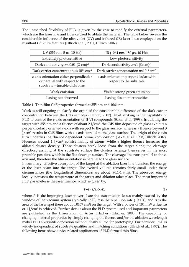
The unmatched flexibility of PLD is given by the ease to modify the external parameters, which are the laser line and fluence used to ablate the material. The table below reveals the considerable influence of the ultraviolet (UV) and infrared (IR) laser lines employed on the resultant CdS film features (Ullrich et al., 2001, Ullrich, 2007):
Dark conductivity σ ≤0.01 (Ω cm)-1 Dark conductivity σ ≈1 (Ω cm)-1
Dark carrier concentration n≈1016 cm-3 Dark carrier concentration n≈1018 cm-3
c-axis orientation either perpendicular or parallel with respect to the substrate – tunable dichroism
c-axis orientation perpendicular with respect to the substrate
Weak emission Visible strong green emission
Lasing not observed Lasing due to microcavities
Table 1. Thin-film CdS properties formed at 355 nm and 1064 nm
Work is still ongoing to clarify the orgin of the considerable difference of the dark carrier concentration between the CdS samples (Ullrich, 2007). Most striking is the capability of PLD to control the c-axis orientation of II-VI compounds (Sakai et al. 1998). Irradiating the target with 355 nm and a fluence of about 2 J/cm2, the CdS film deposited on glass exhibits a perpendicularly oriented c-axis with respect to the glass surface, whereas a fluence beyond 3 J/cm2 results in CdS films with a c-axis parallel to the glass surface. The origin of the c-axis turn underlies the fluence dependent plume composition (Sakai et al. 1998, Ullrich 2007). Fluences around 1 J/cm2 consist mainly of atoms, while a higher fluence increases the ablated cluster density. Those clusters break loose from the target along the cleavage direction; arriving at the substrate surface the clusters arrange themselves in the most probable position, which is the flat cleavage surface. The cleavage line runs parallel to the c-axis and, therefore the film orientation is parallel to the glass surface. In summary, effective absorption of the target at the ablation laser line transfers the energy of the laser beam into the target. The excited volume remains fairly small under these
circumstances (the longitudinal dimensions are about ≤0.1-1 μm). The absorbed energy locally increases the temperature of the target and ablation takes place. The most important PLD parameter is the laser fluence, which is given by,
F=P×l/(R×A), (1)
where P is the impinging laser power, l are the transmission losses mainly caused by the window of the vacuum system (typically 15%), R is the repetition rate (10 Hz), and A is the area of the laser spot (here about 0.0157 cm2) on the target. With a power of 184 mW a fluence of 1 J/cm2 is achieved. Further details about the PLD system used and important parameters are published in the Dissertation of Artur Erlacher (Erlacher, 2005). The capability of changing material properties by simply changing the fluence and/or the ablation wavelength makes PLD a versatile deposition method ideally suited for prototyping. Furthermore, PLD is widely independent of substrate qualities and matching conditions (Ullrich et al., 1997). The following items show device related applications of PLD formed thin films.
www.intechopen.com
Employment of Pulsed-Laser Deposition for Optoelectronic Device Fabrication
587
2. Hybrid logic device formation
With regard to information transmission, all-optical logic operations are very appealing to technological applications since electron based signal processing has certain limitations due to charge storage in capacitors, crosstalk and charge loss or attenuation. However, optical computing – a phrase frequently used in the mid-1980s – remains more or less a fiction and there was disillusion already 20 years ago (Gibbs & Khitrova, 1990) that raised serious doubts regarding the impact non-linear photonics would have on computing. We believe that this development is mainly caused by the circumstance that photonics lacks the inherent ease based on the overwhelmingly perfect mastery of Si (and also GaAs and related compounds), which enables nearly effortless solutions for complex electronic and optoelectronic devices. Hence, it is not a competition between photons and electrons but a struggle between a non-existent technology on an industrial level with the established Si/GaAs industry. The presented results promote PLD formed glass/GaAs interfaces as effective photonic switch media. All-optical and hybrid red laser reflection modulations have been achieved by altering the electronic state of the interface with a green laser. The concept enables the flip from negative to positive logics by solely applying an electric field. Furthermore, reflective femtosecond operations of the interface are demonstrated with pump-probe experiments. Manipulating light with light seems to be an impossible task since photons are gauge bosons and as such not influenced by themselves or by electromagnetic means. Nevertheless, during the 1970’s and 1980’s, notable research efforts revealed ways to make optical computing a reality (Hajto & Janossy, 1983, Gibbs, 1985, Wherrett & Hutchings, 1993). Since then, many switching concepts, various computer architectures, and core materials have been investigated for light driven data transmission (Erlacher et al. 2006, and references therein). Although there are currently various commercially available optical switches, such as the mirror-based Micro-Electro-Mechanical Systems (MEMS) (Shepard, 2001), an overall satisfactory optical switch fabric has not yet been established. In spite of the unsolved switching issue, optical fibers conquer the world of data transportation. Their unmatched transmission speed (currently terabit/s) is capable of bypassing the looming interconnect bottleneck of electric connections. Consequently, as the unit costs keep coming down, fiber to the home (FFTH) might be upon us (Bates, 2001). Neither necessarily linked to concepts described in the “classical” literature (Hajto & Janossy, 1983, Gibbs, 1985, Wherrett & Hutchings, 1993) nor going distinctly along with currently discussed optical techniques in the literature (Papadimitriou, 2007), we introduced all-optical operations via laser crossing (LC) in thin-film semiconductors on glass (Erlacher and Ullrich, 2004, Liyanage et al., 2009). The main advantaging difference between LC and other concepts is its low-cost realization potential due to extreme straightforwardness of the basic principle. Here, we focus on the employment of the glass/GaAs interface as active LC medium for all-optical applications and hybrid computing architectures. The schematic of the experiment is shown in Fig. 4. Red (633 nm) and green (530 nm) continuous wavelength (cw) emissions of a 10 mW He-Ne laser and 20 mW Ar-Kr laser, respectively, were crossed in one spot at the glass/GaAs interface opposite to the opening of Al contacts, which have been evaporated on the film surface. The gap between the contacts was about 1 mm and the impinging laser intensities were kept below 10 W cm-2. The arrangement of the laser rays permitted the measurement of reflection and transmission of the red laser as a function of the on-off sequence of the green laser with the additional
www.intechopen.com
Optoelectronic Devices and Properties
588
option to apply an electric field across the illuminated film area. The reflected and transmitted signals of the He-Ne laser were measured with Si photodiodes, which were connected to amperemeters. The on-off cycling of the Ar-Kr laser beam was achieved by means of an optical shutter.
He-Ne laser (633 nm)
Ar-Kr laser (530 nm)
Interface
Power supply
Glass Thin-film GaAs
Al contact Reflectance Transmittance
Al contact
Optical shutter
Fig. 4. Arrangement of reflective LC at the glass/GaAs interface. Red and green emissions from a He-Ne and Ar-Kr laser, respectively, are crossed at one point oppositely to the gap between two Al contacts on the film surface (US Patent No. 7,826,058)
The GaAs film has been formed with PLD in vacuum (10-3 Pa) by employing the fundamental emission (1064 nm) of the Nd:YAG laser (6 ns, 10 Hz). The target was GaAs:Zn (doping concentration 1019 cm-3) and the film was ablated with a fluence of about 0.8 J cm-2
to be 0.5 μm thick. The distance between target and fused silica glass substrate, which was not heated during the deposition, was 6 cm. It is of interest to briefly discuss the complex texture and unusual high-ohmic behavior of PLD GaAs. We performed x-ray analysis, Raman measurements, and atomic force microscopy (Erlacher et al. 2004 & 2005). Based on these results, the films are of multi-phase nature consisting of microcrystallites, amorphous parts, and nano-sized zincblende migrations. Hall measurements showed acceptor concentration as low as 1013 cm-3, i.e., six orders of magnitude below the target value and one might conclude that the Zn doping of the target vanishes somewhere during PLD. However, secondary ion mass spectroscopy (SIMS) showed that the Zn concentration in the films is maintained but due to the peculiar texture the impurities are hardly electrically
active. This observation explains the measured resistance of >109 Ω between the two evaporated Al contacts. From this point of view, low-temperature PLD GaAs on glass refers to dielectric material rather than to typical semiconductors. It is worthwhile to note that the motivation for the interface investigations came from photoluminescence (PL) measurements rather than from previous switching experiments. Comparing the PL excited at the surface and through the glass substrate, we recognized that PLD CdS on glass exhibits an increased absorption at the glass/CdS interface with respect to the rest of the film (Ullrich & Schroeder a, 2001, Ullrich and Schroeder b, 2001). Hence, we
www.intechopen.com
Employment of Pulsed-Laser Deposition for Optoelectronic Device Fabrication
589
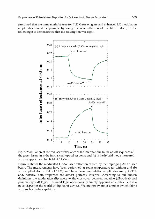
presumed that the same might be true for PLD GaAs on glass and enhanced LC modulation amplitudes should be possible by using the rear reflection of the film. Indeed, in the following it is demonstrated that the assumption was right.
0.14
0.16
0.18
0.20
0.22
0.24(a) All-optical mode (0 V/cm), negative logic
Ar-Kr laser on
Ar-Kr laser off
0.14
0.16
0.18
0.20
0.22
0.24
0 5 10 15 20 25 30 35
Time (s)
(b) Hybrid mode (6 kV/cm), positive logic
Ar-Kr laser on
Ar-Kr laser off
Inte
rface
ref
lect
an
ce a
t 633 n
m
Fig. 5. Modulation of the red laser reflectance at the interface due to the on-off sequence of the green laser: (a) is the intrinsic all-optical response and (b) is the hybrid mode measured with an applied electric field of 6 kV/cm
Figure 5 shows the modulated He-Ne laser reflection caused by the impinging Ar-Kr laser beam. The measurements have been performed at room temperature (a) without and (b) with applied electric field of 6 kV/cm. The achieved modulation amplitudes are up to 35% and, notably, both responses are almost perfectly inverted. According to our chosen definition, the modulation flip refers to the cross-over between negative (all-optical) and positive (hybrid) logics. To invert logic operations by simply applying an electric field is a novel aspect in the world of digitizing devices. We are not aware of another switch fabric with such a useful capability.
www.intechopen.com
Optoelectronic Devices and Properties
590
According to Fig. 5, around 15% and more of the red laser light was reflected and for the reflected portion of the green laser we found 30%. Thus, with consideration of the losses in the lenses used to adjust the laser beams, the overall optical power dissipated in the film did not exceed 20 mW. It was demonstrated in a previous publication (Ullrich et al., 2004) that a moderate laser power like that only marginally warms up the GaAs sample and does not cause noticeable photothermal effects, i.e., the observation in Fig. 5 (a) is driven by the alteration of the local electronic state of the film. The same is true for the hybrid operation. Due to the extreme resistance of the sample, the dissipated electrical power under illumination did not exceed 10-4 W and, therefore, is certainly not the origin of modulation flip in Fig. 5 (b) with respect to the all-optical mode in Fig. 5 (a). The inversion of the modulation is rather caused by the reduction of the electron number available for absorption transitions, i.e., with growing electric field more and more electrons join the circulation of the photocurrent rather than to maintain the matrix element of the absorption coefficient due to recombination into the valence band. As a consequence, the sample becomes more transparent and the modulation sequence is inverted in Fig. 5 (b) with respect to Fig. 5 (a). Figure 6 reveals the dependence of the modulation amplitude on the applied electric field of the reflected and transmitted signal of the He-Ne laser. Positive and negative signs of the modulation amplitude correspond to positive and negative logic.
-30
-20
-10
0
10
20
30
40
0 1 2 3 4 5 6
Mo
du
lati
on
am
pli
tud
e (
%)
Electric field (kV/cm)
Positive logic
Negative logic
(a) Re at 633 nm
(b) Tr at 633 nm
Interface
Fig. 6. The modulation amplitude vs. electric field of (a) the reflectance (Re) and (b) transmittance (Tr) of the He-Ne laser measured at the glass/GaAs interface. Positive and negative signs refer to positive and negative logic, respectively. The solid and broken lines are guides for the eyes
For comparison, Fig. 7 shows the corresponding LC results for the thin-film, i.e., the film side was excited as in previous works (Erlacher and Ullrich, 2004, Ullrich et al. 2004). The film reflection exhibits almost no modulation, whereas the maximum of the transmission
www.intechopen.com
Employment of Pulsed-Laser Deposition for Optoelectronic Device Fabrication
591
modulation is comparable with the results in Fig. 6, while, as suspected from the PL results (Ullrich & Schroeder a, 2001, Ullrich and Schroeder b, 2001), at the interface, more absorption transitions are excited with the same amount of impinging photons than at the film surface itself. Furthermore, from the viewpoint of device engineering, with the employment of the reflected beam effective fan-out is easier to achieve than with the much weaker transmitted signals, which were approximately 0.8% and 0.2%, for the red and green laser, respectively.
-8
-6
-4
-2
0
2
4
6
8
0 1 2 3 4 5 6
Mo
du
lati
on
am
pli
tud
e (%
)
Electric field (kV/cm)
Positive logic
Negative logic
Film
(b) Tr at 633 nm
(a) Re at 633 nm
Fig. 7. Corresponding results to Fig. 6 measured at the film side
Equivalently to Fig. 4, pump-probe experiments have been performed at room temperature
by replacing the green cw laser irradiation with green (532 nm) ultrafast (<100 fs) laser
pump pulses with a repetition rate of 1 kHz, and, instead with the He-Ne laser, the interface
was probed with white light continuum. The reflected spectrum was guided in a fiber
spectrometer. A typical result of the reflection kinetics for 633 nm is shown in Fig. 8, which
depicts the ratio of the reflection without pump over the reflection with pump (Re0/Re).
Turn-on and recovery time are extremely fast resulting in a kinetics profile with a full width
at half maximum (FWHM) of about 600 fs. Hence, in contrast to the thin-film itself whose
recovery time exceeded more than 10 ps (Ullrich et al., 2004), metastable states with unusual
short lifetimes in the fs range are generated at the glass/GaAs interface. It is worth
mentioning that our temporally resolved reflection alteration takes place on a similar time
scale as the transmission kinetics of CdTe nanocrystals (Padilha, 2005) and our observed
recovery time can be compared with that in Bragg-spaced quantum well structures
(Johnston, 2005).
www.intechopen.com
Optoelectronic Devices and Properties
592
0.998
0.999
1.000
1.001
1.002
1.003
1.004
0 1 2 3 4 5 6 7 8
Re
0/Re
Time (ps)
Interface
Fig. 8. Ultrafast reflection kinetics of the glass/GaAs interface at 633 nm. The ordinate shows the signal without pump pulse (Re0) over the signal with the pump pulse (Re)
3. Hybrid photosensitive device formation
The need for operative optoelectronic devices composed of various semiconductors is based
on technological requirements as well as economical arguments, while in many cases
simultaneous improvement of both branches is anticipated. In particular, operative hetero-
pairing of GaAs and Si has been pursued for quite some time owing to its considerable
technological importance for efficient and low-cost photovoltaic and optoelectronic devices
(Alberts et al., 1994). However, GaAs-on-Si formations are not a straightforward task. The
mismatch of thermal expansion coefficients (60%) and lattice constants (4%) causes stress in
the film during deposition and the formation of defect states at the film substrate interface,
respectively. Besides improvement of the electrical and structural properties of the GaAs/Si
heterostructure can be achieved using a ZnSe (Lee et al., 1994) or SrTiO3 (internet, 2001)
buffer layer, direct growth and deposition were pursued by using a wide range of methods
since several decades with varying success and satisfaction. For example, the direct growth
of GaAs on Si employing MBE was studied (Usui et al., 2006).
Concerning the hetero-pairing of PLD GaAs with Si, previous research mainly focused on
rectifying properties and bias dependent alternating photocurrent (APC) of p-GaAs on n-Si
www.intechopen.com
Employment of Pulsed-Laser Deposition for Optoelectronic Device Fabrication
593
(Ullrich and Erlacher a, 2005, Ullrich and Erlacher b, 2005). Here, stoichiometry, surface
morphology, crystallographic properties, and quality of rectification of PLD formed n-GaAs
on p-Si heterostructures were studied. In addition, the bias dependence of APC spectra and
direct photocurrent (DPC) spectra is demonstrated.
The deposition of GaAs onto Si was carried out with the second harmonic emission at 532
nm of the Q-switched Nd:YAG laser (6 ns, 10 Hz). The substrate was boron (B) doped prime
grade 250-300 μm thick p-type Si (100) wafer and the target was tellurium (Te) doped n-type
GaAs (100) with a doping concentration of 1.3-3.4×1018 cm-3. As usual, the rotating (16 rpm)
GaAs target was kept at 45º with respect to the impinging laser beam. The rotation was
performed in order to ablate the material homogeneously. Parallel to the ablation area of the
target, the substrate was mounted 6 cm above the target. The deposition was carried out in
vacuum of 6.7×10⁻⁵ Pa without heating the substrate in order to avoid interface stress and
deformation during cooling. The target was exposed to a laser fluence of 0.98 ±0.1 J/cm2 for
one hour resulting in a GaAs film with a thickness of about 600 nm. In order to perform
APC and DPC measurements, electrical contacts were made with evaporated aluminum (Al)
to the surface and by silver (Ag) paste to the rear of the sample.
Stoichiometry, crystallographic properties, and surface quality of the GaAs film were
investigated by electron probe micro-analyzer (EPMA) technique, x-ray diffraction, and
scanning electron microscopy (SEM), respectively. The current-voltage (I-V) characteristic,
of the heterojunction was measured in the dark by sweeping the applied bias between the
Al and Ag contacts with a programmable source meter. The APC spectra were measured
with lock-in technique by exciting the sample surface with chopped (107 Hz) light, while
steady-state illumination and a pico-amperemeter were used to record the DPC responses.
The sample was irradiated with a 200 W halogen lamp, whose emission was
monochromatically dispersed with a ½ m monochromator. Excitation light was passed
through a long pass filter and the photon energy was varied from 1.1 to 1.80 eV and the
biases were applied using a programmable power supply. The PC was measured vertically
through the device using contacts 0 and 1 or laterally employing contacts 1 and 2 as
schematically shown in Fig. 9. All the PC spectra shown have been corrected with a
calibrated Si photodiode in order to express the results in terms of responsivity (A/W). All
measurements were carried out at room temperature. The EPMA results show Ga and As concentrations of 48.80 (at. %) and 51.20 (at. %), respectively. Hence, low-temperature PLD forms quasi-stoichiometric GaAs films on Si with a slight As surplus. The slight deviation of stoichiometry reflects the trend known from MBE formed GaAs, i.e., the growth of GaAs at low substrate temperatures results in GaAs with excess As incorporated into the GaAs matrix (Ma et al., 2004), which is amorphous as the x-ray result in Fig. 10 reveals. The only GaAs related peak observed is the fairly faint feature at 27.25 degree indicating that the film texture is predominately of amorphous nature embedding small portions of crystallites. We should stress that previous x-ray investigations on n-GaAs/p-Si did not show peaks, presumably due to the extremely thin film. The SEM image, (Acharya et al., 2009), shows droplet-like micron-sized clusters. With selectively performed Raman measurements, we found that these clusters are single crystalline GaAs, which are not grown but directly transferred from the target during PLD (Erlacher et al. 2006). Since these droplets increase the surface area, the formed hetero-pairing has the potential to be used as chemical sensors and chemical reaction catalysts.
www.intechopen.com
Optoelectronic Devices and Properties
594
Power supply Lock-in amplifier
Ag (0)
Al (1)
Si Chopper
Monochromatic light
Al (2)
PLD-GaAs
Fig. 9. Experimental setup used for the APC measurements. DPC was measured without chopper and the lock-in amplifier was replaced with a pico-amperemeter
200
250
300
350
20 22 24 26 28 30
2Θ (degree)
X-r
ay
in
ten
sity
(cou
nts
) (111)
Fig. 10. X-ray pattern of the GaAs film
The dark I-V characteristic of the n-GaAs/p-Si device is shown in Fig. 11. The device showed rectification and the symbols represent the measurements, while the solid line visualizes close fit of the forwardly biased I-V curve using the common diode equation (Fahrenbruch &Bube, 1983),
www.intechopen.com
Employment of Pulsed-Laser Deposition for Optoelectronic Device Fabrication
595
bs exp 1β⎛ ⎞⎡ ⎤= −⎜ ⎟⎢ ⎥⎜ ⎟⎣ ⎦⎝ ⎠
eVI I
kT, (2)
where, Is is the saturation latching current, e is the elementary charge, Vb is the applied bias, β is a factor taking into account deviations from the ideal diode characteristic, and kT (=25
meV) is the thermal energy. The fit delivered the following values: Is=2.01×10⁻⁷ A and β=35.2. The applicability of Eq. (2) is quite notable since it did not apply for p-GaAs/n-Si
hetero-structures (Ullrich and Erlacher a, 2005), which required a modified version of Eq. (2)
in order to fit the forward current.
10
-4
10-5
10-6
10-7
10-8
0 1 2 3 4 5
Voltage (V)
Cu
rren
t (A
)
Fig. 11. I-V characteristic of the junction measured using contacts 1-0 in Fig. 9. The symbols represent the measurements and the solid line the fit using Eq. (2)
The doping of the target and its reestablishment in the deposited film was investigated.
Comparing the results of SIMS and Hall measurements for p-GaAs/n-Si samples, we
established that the physical concentration of doping atoms in the film closely corresponds
to the target level but, due to the amorphous film texture, the concentration of electronically
active dopants in the film is several orders of magnitude below the initial target value
(Ullrich et al. 2008). Since the texture of n-GaAs deposited on p-Si is amorphous as well, we
conclude that the improved diode features of the current sample is most likely caused by a
comparably more abrupt interface with less recombination centers and charge alignments,
allowing the exponential dependence on the bias.
www.intechopen.com
Optoelectronic Devices and Properties
596
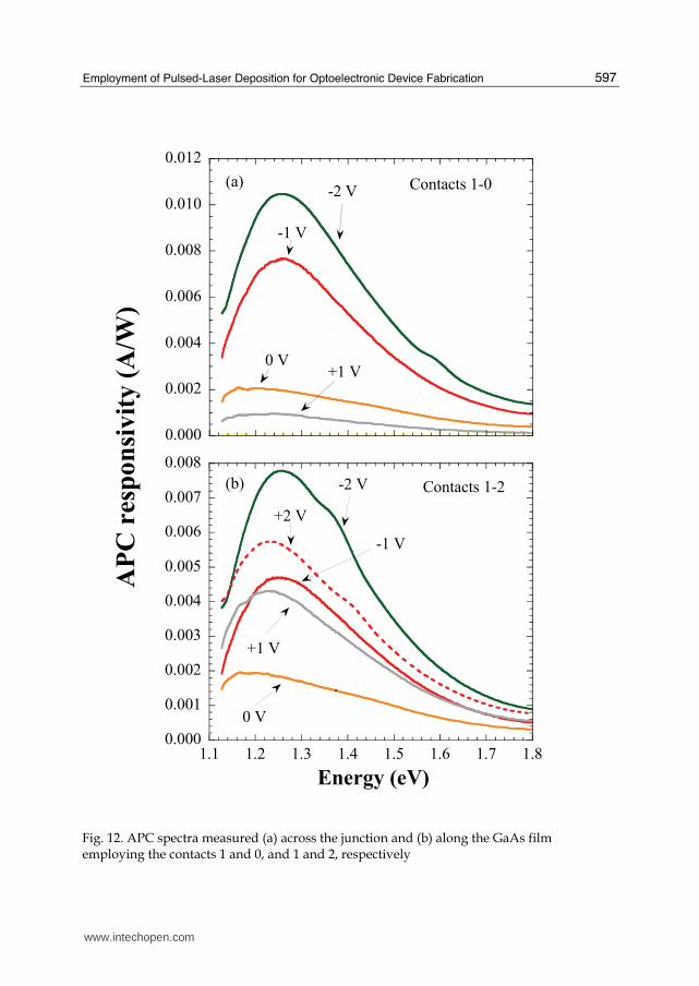
The APC responsivity across the sample was measured by using contact combination 1-0
and 1-2 for various biases shown in Figs. 12 (a) and 12 (b). We first discuss the results in Fig.
12 (a). Negative bias signs mean that contact 0 (p-Si) was connected to the negative terminal
of the power supply, corresponding to backward polarity, whereas positive signs indicate
forward bias direction. Figure 12 (a) reveals all the features of an operating photodiode: a)
The hetero-structure is sensitive to light without bias, b) increase in APC under reverse bias
points to enlargement of the depletion layer, while c) a forward bias shrinks the depletion
layer making the structure less light sensitive. In fact, the APC is completely bleached at a
bias of +2 V on a linear scale.
Comparing the results shown here with the spectra of p-GaAs/n-Si photodiodes
investigated in detail in Ref. Ullrich & Erlacher b, 2005, the most notable difference is the
spectral shape of the intrinsic APC shown in Fig. 13. We should stress that despite the
inverted doping, both samples in Fig. 13 have been formed under the same conditions. The
n-GaAs/p-Si hetero-pairing exhibits APC in the absorption range of GaAs and Si, while the
responsivity of the p-GaAs/n-Si is clearly dominated by the absorption in the Si substrate
with trifling contributions of the GaAs film. The GaAs film contributes to the photocurrent if
the depletion width in the GaAs film is comparable to that in the Si substrate, or, at least the
diffusion length of the minority carriers in the GaAs film is long enough to reach the
depletion region in Si (Ullrich et al., 1999). Obviously, this condition is not fulfilled for the p-
GaAs/n-Si sample. Furthermore, forward bias induced APC bleaching is much less effective
for the p-GaAs/n-Si structures and, while the energy position of the APC maxima in Fig. 12
(a) does not depend on bias polarity, the APC peak of p-GaAs/n-Si samples undergoes a
shift of ≈100 meV by flipping the bias from +1 V to –1 V. These observations - in
combination with the result revealed in Fig. 11 - clearly point to the fact that low-
temperature PLD of n-GaAs onto p-Si forms the more defined junction device with clearly
improved operational features.
The APC responsivities achieved with contacts 1 and 2 for different biases are shown in Fig.
12 (b). The sign notation refers to a polarity change rather than to a specific bias direction
since we measure along the GaAs layer. The APC grows with increase in bias in either
direction as expected from a common photoconducting material. Ideally, the photoresponse
of the sample ought to be symmetric, i.e., the same APC spectrum is expected for either
polarity. The difference in the spectra is most likely caused by inequalities of the Al
electrodes. Notably, the sample showed responsivity at 0 V, like a diode though the current
was not measured across the junction. The reason is discussed below. The DPC responsivity spectra of the sample using contacts 1 and 0 are shown in Fig. 14 (a). The results correspond to these in Fig. 12 (a) besides the forwardly biased sample did not expose DPC, while a fairly weak DPC at 0 V took place. The latter is negative because in the measuring configuration employed the positive terminal of the amperemeter was connected with the n-side of the sample. The spectra in Fig. 14 (b) measured with the contacts 1 and 2 expose the features of a semiconducting layer like in Fig. 12 (b), showing a similar broken symmetry. However, in contrast to the APC measurements, the DPC shows only a very
weak (<50 μA/W) signal for 0 V. Hence, the DPC spectra reveal a behavior much closer to expectation than the zero biased APC measurements. The answer to this apparent contradiction lies in the fact that the APC at 0 V measures the light dependence of the charging current of the device capacity rather than its responsivity, and, as a consequence, the APC spectra for 0 V barely depend on the contact configuration.
www.intechopen.com
Employment of Pulsed-Laser Deposition for Optoelectronic Device Fabrication
597
0.000
0.002
0.004
0.006
0.008
0.010
0.012
Contacts 1-0-2 V
-1 V
0 V+1 V
(a)
AP
C r
esp
on
sivit
y (
A/W
)
0.000
0.001
0.002
0.003
0.004
0.005
0.006
0.007
0.008
1.1 1.2 1.3 1.4 1.5 1.6 1.7 1.8
Energy (eV)
-2 V
+2 V
-1 V
+1 V
0 V
Contacts 1-2(b)
Fig. 12. APC spectra measured (a) across the junction and (b) along the GaAs film employing the contacts 1 and 0, and 1 and 2, respectively
www.intechopen.com
Optoelectronic Devices and Properties
598
0.0000
0.0005
0.0010
0.0015
0.0020
1.1 1.2 1.3 1.4 1.5 1.6 1.7 1.8
AP
C r
esp
on
siv
ity
(A
/W)
Energy (eV)
n-GaAs/p-Si
p-GaAs/n-Si
Contacts 1-0, 0 V
Fig. 13. Comparison of the APC responsivity at 0 V for n-GaAs/p-Si in Fig. 12 (a) and for p-GaAs/n-Si taken from Fig. 4 in Ref. Ullrich & Erlacher b (2005)
-0.012
-0.010
-0.008
-0.006
-0.004
-0.002
0.000
0.002
0 V
-1 V
-2 V
Contacts 1-0(a)
-0.010
-0.005
0.000
0.005
1.1 1.2 1.3 1.4 1.5 1.6 1.7 1.8
Energy (eV)
Contacts 1-2+2 V
+1 V
0 V
-2 V
-1 V
(b)
DP
C r
esp
on
siv
ity
(A
/W)
Fig. 14. DPC spectra (a) measured across the junction and (b) along the GaAs film employing the contacts 1 and 0, and 1 and 2, respectively
www.intechopen.com
Employment of Pulsed-Laser Deposition for Optoelectronic Device Fabrication
599
Concluding, we have presented a detailed study of thin-film n-GaAs deposited onto p-Si using nanosecond laser ablation. The results demonstrate that low-temperature PLD delivers stoichiometric GaAs films, which have some crystalline sections embedded in an amorphous matrix. The appearance of the film surface is very similar to GaAs/glass samples, i.e., smooth with some spherical micron-sized droplets on top. It is clearly worthwhile to stress that the achieved optoelectronic results here are quite different from previous investigations on p-GaAs/n-Si samples. Most striking is that the deposition of n-GaAs on counter-doped Si results in a pn-junction, which is accurately described by the common diode equation. The opposite material combination, however, exhibits a peculiar, but nevertheless rectifying, I-V characteristic. The responsivity features go along with the I-V curves: Contrasting the results in Ullrich B. & Erlacher A. b (2005), the junction spectra did not shift when a reverse bias was applied, pointing to a depletion region with a defined uniform band gap, and, at a fairly low bias of 2 V, the APC was drastically bleached. The APC results were confirmed with DPC investigations. In this context, by measuring the responsivity along the GaAs film, the work further stresses that intrinsic features (meaning intrinsic solely from the electronic viewpoint) measured with lock-in technique do not necessarily correspond to the intrinsic ground state of the device investigated.
4. Summery and future developments
Formation of thin-film device structures with low-temperature PLD is a very active, appealing and extremely versatile applied research field. PLD is in particular well suited for the production of operative optoelectronic/photonic device prototypes such as the GaAs-on-glass merger and GaAs/Si photodiodes. Low-temperature PLD opens another door of fruitful research: The formation of predominantly amorphous thin films, which reveal quantum-confined features (Acharya et al., 2007). Ongoing work on nanostructured CdS films on flexible polyethylene terephthalate (PET) substrates formed with nanosecond low-temperature PLD is a promising alternative to fragile, rigid device structures. The film consists of intrinsically formed self-assembled ~ 100 nm grains speckled with CdS 10-20 nm quantum dots. The films are stoichiometric and show blue shifted photocurrent spectra due to quantum confinement. The nanocrystal size of about 6 nm calculated from the photocurrent peak shift agrees reasonably well with the texture analysis. Similar results have been achieved currently with ZnTe. Due to the complex and therefore electronically sensitive texture, the hybrid merger of high-absorptive materials such as GaAs or CdS on plastic is an ideal host for logic devices based on LC using common visible laser sources. Promising preliminary results including optoelectronic and photonic operations have been demonstrated and discussed here. Figure 15 shows one of the advanced results at present under investigation. By superposition of red (632.8 nm) and blue (488.0 nm) cw laser irradiation in the same spot of the GaAs thin-film surface, i.e., by additional irradiation with the red laser line, the reflected spot (a) of the blue line changed to a ring-like pattern (b). The effect can be used as photonic laser steering without externally provided mechanical means. The effect is most likely caused by the formation of a photothermal lens due to mechanical deformation of the plastic substrate caused by the warming of the GaAs top layer. Eventually, future photonic data transfer technologies will employ laser pattern alterations and laser steering by non-mechanical means (Liyanage et al., 2009).
www.intechopen.com
Optoelectronic Devices and Properties
600
Red laser line
Blue laser line
Plastic substrate
Thin-film GaAs
(a)
(b)
Fig. 15. Laser steering by superposition of two laser lines using a GaAs/plastic hetero-pair
5. References
George J. (1992). Preparation of Thin Films, Marcel Dekker, ISBN 0-8247-8196-1, New York Smith D. L. (1995). Thin-film Deposition, Principles & Practice. MacGraw-Hill Inc., ISBN 0-07-
058502-4, New York Ullrich B., Zhang C. & v. Klitzing K. (1988). Quantum-confined subband transitions of GaAs
sawtooth doping superlattices, Appl. Phys. Lett., Vol. 54, Issue 12, 1133-1135 Bouchenaki C. a, Ullrich B. & Zielinger J. P. (1991). Luminescence investigations performed
on differently prepared thin CdS layers. J. Luminescence, Vol. 48&49, Part 2, 649-654 Bouchenaki C. b, Ullrich B., Zielinger J. P., Cong H. N. & Chartier P. (1991). Preparation,
characterization and bistable photoconduction of thin CdS layers. J. Opt. Soc. Am. B, Vol. 8, Issue 3, 691-700
Ullrich B., Kulac I. & Pint H. (1992). Photocurrent in thin YBa2Cu3O6 films on sapphire. Jap.
J. Appl. Phys., Vol. 31, No. 7A, L856-L859 Ullrich B. & Kobayashi T. (1995). A new architecture for optical data processing devices by
the application of bistability in luminescence. Optical Review, Vol. 2, No. 1, 43-46 Ullrich B., Erlacher A., Yano S., Schroeder R., Gerasimov T. G. & Haugan H. J. (2003).
Preparation of thin-film GaAs on glass by pulsed-laser deposition. Proceedings of SPIE 4977, pp. 180-187, Photonics West, San Jose
www.intechopen.com
Employment of Pulsed-Laser Deposition for Optoelectronic Device Fabrication
601
Acharya K. P., Mahalingam K., & Ullrich B. (2010). Structural, compositional, and optoelectronic properties of thin-film CdS on p-GaAs prepared by pulsed-laser deposition. Thin Solid Films, Vol. 518, Issue 7, 1784-1787
Ezumi H. & Keitoku S. (1993). Influence of pulse width on CdS film prepared by YAG laser ablation. Jap. J. Appl. Phys. Vol. 32, Issue 4R, 1783-1786
Ullrich B. (2007). Thin-film CdS formed with pulsed-laser deposition towards optical and hybrid device applications. J. Mater. Sci.: Mater. Electron, Vol. 18, 1105-1108
Sakai H., Tamaru T., Sumomogi T., Ezumi H. & Ullrich B. (1998). Crystal direction of CdS thin films produced by laser ablation. Jap. J. Appl. Phys. Vol. 37, 4149-4153
Erlacher A. (2005). Pulsed-laser deposition and characterization of hetero-paired thin-film GaAs. Dissertation BGSU. Source ProQuest DAI-B 66/10, p. 5459, Apr. 2006.
Ullrich B., Sakai H., Dushkina N. M., Ezumi H., Keitoku S. & Kobayashi T. (1997). The effect of the substrate on the emission features of thin CdS films formed by laser ablation. Mater. Sci. Eng. B Vol. 47, Issue 2, 187-189
Gibbs H. M. & Khitrova G. (1990). Introduction, in Nonlinear Photonics, Gibbs H. M., Khitrova G. & Peyghambarian N. (Eds.), 1-3, Springer, ISBN-10 0387521941, Berlin
Hajto J. & Janossy I. (1983). Optical Bistability observed in amorphous semiconductor films. Phil. Mag. B Vol. 47, 347-366
Gibbs H. M. (1985). Optical Bistability: Controlling light with light, Academic Press, ISBN-10 0122819411, San Diego.
Wherrett B. S. & Hutchings D. C. (1993). Optical bistability, In: Nonlinear Optics in Signal Processing, Eason R. W., Miller A. (Ed.), 145-189, Chapman & Hall, 0 412 39560 6, London
Erlacher A., Danilov E. O. & Ullrich B. (2006). Introduction of glass/GaAs interfaces for all-optical and hybrid switch fabrics. Semicond. Sci. Technol. Vol. 21, No. 9, 1331-1334
Shepard S. (2001). Optical Networking Crash Course, McGraw Hill, ISBN 0-07-137208-3, New York
Bates R. J. (2001). Optical Switching and Networking Handbook, MacGraw Hill, ISBN 0-07-137356-X, New York
Papadimitriou G. I, Papazoglou C. & Pomportsis A. S. Optical Switching, Wiley & Sons, ISBN-10 0-471-68596-8, Hoboken
Erlacher A. & Ullrich B. (2004). All-optical digitizing of laser transmission through thin-film GaAs on glass. Semicond. Sci. Technol. Vol. 19, L9-L12
Liyanage C., Acharya K. & Ullrich B. (2009). Photonic digitizing and pattern alteration with flexible CdS and GaAs film surfaces. J. Opt. Soc. B, Vol. 26, Issue 2, 254-258
Erlacher A., Ambrico M.. Capozzi V., Augelli V., Jaeger H. & Ullrich B. (2004). X-ray, absorption and photocurrent properties of thin-film GaAs on glass formed by pulsed-laser deposition. Semicond. Sci. Technol. 19 No. 11, 1322-1324
Erlacher A., Ullrich B., Komarova E. Y., Jaeger H., Haugan H. J. & Brown G. J. (2006). Texture and surface analysis of thin-film GaAs on glass formed by pulsed-laser deposition. J. Non-Cryst. Solids, Vol. 352, Issue 2, 193-196
Ullrich B. a & Schroeder R. (2001). Green single- and two-photon gap emission of thin film CdS formed by infrared pulsed-laser deposition on glass. IEEE J. Quantum Electron. Vol. 37, No. 10, 1363-1367
Ullrich B. b & Schroeder R. (2001). Intrinsic gap emission and its geometry dependence of thin-film CdS excited by two-photon absorption. Semicond. Sci. Technol. 16, No. 12, L89-L92
www.intechopen.com
Optoelectronic Devices and Properties
602
Ullrich B., Erlacher A. & Danilov E. O. (2004). Switch performance and electronic nature of photonic laser digitizing through thin GaAs films on glass. Semicond. Sci. Technol. Vol. 19, No. 12, L111-L114
Padilha L. A., Neves A. A. R., Rodriguez E., Cesar C. L., Barbosa L. C. & Brito Cruz C. H. (2005).Ultrafast switching with CdTe nanocrystals in a glass matrix. Appl. Phys. Lett. Vol. 86, 161111 (3 pages)
Johnston W. J., Yildirim M., Prineas J. P., Smirl A. L., Gibbs H. M. & Khitrova G. (2005). All-optical spin-dependent polarization switching in Bragg-spaced quantum well structures. Appl. Phys. Lett. Vol. 87, 101113 (3 pages)
Alberts V., Neethling J. H. & Leitch A. W. (1994). Correlation between structural, optical, and electrical properties of GaAs grown on (001) Si. J. Appl. Phys., Vol. 75, Issue 11, 7258-7265
Lee M. K., Horng R. H., Wuu D. S. & Chen P. C. (1991). Improvements in the heteroepitaxy of GaAs on Si by incorporating a ZnSe buffer layer. Appl. Phys. Lett. Vol., 59, Issue 2, 207-209
Internet (2001), Motorola grows GaAS on Si http://www.thinfilmmfg.com/Noteworthy/Noteworthy01/GaAs20Sept01.htm Usui H., Ishiji K., Yasuda H. & Mori H. (2006). Growth process and nanostructure of
crystalline GaAs on Si (110) surface perpared by molecular beam epitaxy. J. Cryst. Growth, Vol . 289, Issue 1, 76-80
Ullrich B. & Erlacher A. a (2005). Rectification and intrinsic photocurrent of GaAs/Si photodiodes formed with pulsed-laser deposition at 1064 nm. Appl. Phys Lett., Vol. 87, 151115 (3 pages)
Ullrich B. & Erlacher A. b (2005). Photosensitive hetero-pairing of p-GaAs/n-Si by pulsed-laser deposition. J. Phys. D: Appl. Phys., Vol. 38, No. 22, 4048-4052
Ma K., Urata R., Miller D. A. B. & Harris J. S. Jr. (2004). Low-temperature growth of GaAs on Si used for ultrafast photoconductive switches. IEEE J. Quantum Electron., Vol. 40, No. 6, 800-804
Acharya K. P., Khatri H. & Ullrich B. (2009). Physical characterization of n-GaAs on p-Si formed by low-temperature pulsed-laser deposition. (2009). J. Appl. Phys. Vol. 105, 103111 (5 pages)
Fahrenbruch A. L. & Bube R. H. (1983). Fundamentals of Solar Cells: Photovoltaic Solar Energy Conversion, Academic Press, ISBN 0122476808, New York
Ullrich B., Erlacher A., Smith H. E., Mitchel W. C. & Brown G. J. (2008). Electronic properties of p-GaAs deposited on n-Si with pulsed laser deposition. J. Phys.: Condens. Matter Vol. 20, 175217 (3 pages)
Ullrich B., Loeher T., Segawa Y. & Kobayashi T. (1999). The influence of hydrogen passivation of silicon on the photocurrent of CdS/Si heterodiodes. Mater. Sci. Eng. Vol. 65, Issue 3, 150-152
Acharya K. P., Skuza J. R., Lukaszew R. A., Liyanage C. & Ullrich B. (2007). CdS thin films formed on flexible plastic substrates by pulsed-laser deposition. J. Phys.: Condens. Matter, Vol. 19, No. 19, 196221 (5 pages)
www.intechopen.com
Optoelectronic Devices and PropertiesEdited by Prof. Oleg Sergiyenko
ISBN 978-953-307-204-3Hard cover, 660 pagesPublisher InTechPublished online 19, April, 2011Published in print edition April, 2011
InTech ChinaUnit 405, Office Block, Hotel Equatorial Shanghai No.65, Yan An Road (West), Shanghai, 200040, China
Phone: +86-21-62489820 Fax: +86-21-62489821
Optoelectronic devices impact many areas of society, from simple household appliances and multimediasystems to communications, computing, spatial scanning, optical monitoring, 3D measurements and medicalinstruments. This is the most complete book about optoelectromechanic systems and semiconductoroptoelectronic devices; it provides an accessible, well-organized overview of optoelectronic devices andproperties that emphasizes basic principles.
How to referenceIn order to correctly reference this scholarly work, feel free to copy and paste the following:
Ullrich Bruno (2011). Employment of Pulsed-Laser Deposition for Optoelectronic Device Fabrication,Optoelectronic Devices and Properties, Prof. Oleg Sergiyenko (Ed.), ISBN: 978-953-307-204-3, InTech,Available from: http://www.intechopen.com/books/optoelectronic-devices-and-properties/employment-of-pulsed-laser-deposition-for-optoelectronic-device-fabrication