92
ENE 334 Microprocessors Page 1 Lecture 8: MCS-51 Architecture II http://webstaff.kmutt.ac.th/~dejwoot.kha/ Week #08 : Dejwoot KHAWPARISUTH

ENE 334 Microprocessors
Page 1
Lecture 8:
MCS-51 Architecture II
http://webstaff.kmutt.ac.th/~dejwoot.kha/
Week #08 : Dejwoot KHAWPARISUTH

Outlines:
Page 2
➔ 8051 Microcontroller Hardware
➔ Input/Output Pins, Ports, and Circuits
➔ External Memory ➔ Counters and Timers ➔ Serial Data I/O ➔ Interrupts
Week #08 ENE 334 MCS-51 Architecture II

8051: Stack Operation
Page 3
The stack refers to an area of internal RAM that is used in
conjunction with certain opcodes to store and retrieve data
quickly. The 8-bit Stack Pointer (SP) register is used by the
8051 to hold an internal RAM address that is called the top
of the stack. The address held in the SP register is the
location in internal RAM where the last byte of data was
stored by a stack operation.
ENE 334 MCS-51 Architecture II Week #08

8051: Stack Operation
Page 4
When data is to be placed on the stack, the SP increments
before storing data on the stack so that the stack grows up
as data is stored. As data is retrieved from the stack, the
byte is read from the stack, and then the SP decrements to
point to the next available byte of stored data.
ENE 334 MCS-51 Architecture II Week #08

8051: Stack Operation
Page 5 ENE 334 MCS-51 Architecture II Week #08
8051: Stack Operation
Page 6
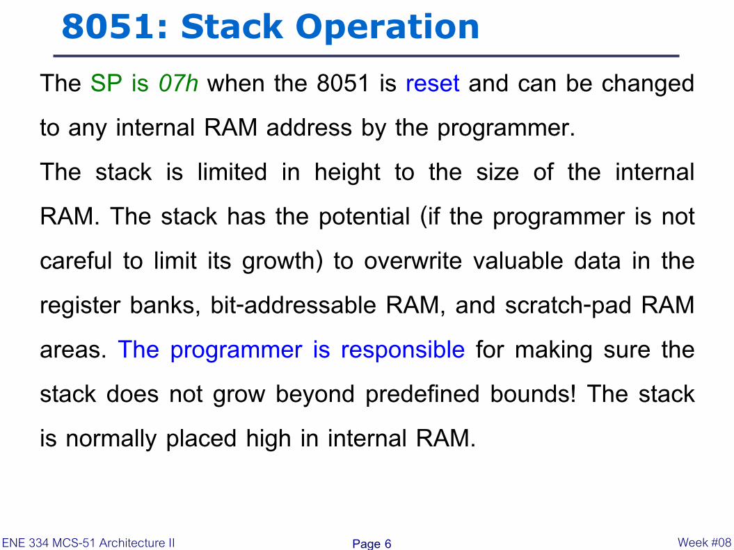
The SP is 07h when the 8051 is reset and can be changed to any internal RAM address by the programmer. The stack is limited in height to the size of the internal RAM. The stack has the potential (if the programmer is not careful to limit its growth) to overwrite valuable data in the register banks, bit-addressable RAM, and scratch-pad RAM areas. The programmer is responsible for making sure the stack does not grow beyond predefined bounds! The stack is normally placed high in internal RAM.
ENE 334 MCS-51 Architecture II Week #08

8051: SFR
Page 7
The 8051 operations that do not use the internal 128-byte RAM addresses from 00h to 7Fh are done by a group of specific internal registers, each called a Special-Function register (SFR), which may be addressed much like internal RAM, using addresses from 80h to FFh. Some SFRs are also bit addressable, as is the case for the bit area of RAM. This feature allows the programmer to change only what needs to be altered.
ENE 334 MCS-51 Architecture II Week #08

8051: SFR
Page 8
Not all of the addresses from 80h to FFh are used for
SFRs, and attempting to use an address that is not
defined, or empty, results in unpredictable results.
ENE 334 MCS-51 Architecture II Week #08

8051: SFR
Page 9 ENE 334 MCS-51 Architecture II Week #08

8051: Internal ROM
Page 10
The 8051 is organized so that data memory and program
code memory can be in two entirely different physical
memory entities. Each has the same address ranges. A
corresponding block of internal program code, contained in
an internal ROM, occupies code address space 0000h to
0FFFh. The PC is ordinarily used to address program code
bytes from addresses 0000h to FFFFh.
ENE 334 MCS-51 Architecture II Week #08

8051: Internal ROM
Page 11
Program addresses higher than 0FFFh, which exceed the internal
ROM capacity, will cause the 8051 to automatically fetch code
bytes from external program memory. Code bytes can also be
fetched exclusively from an external memory, addresses 0000h to
FFFFh, by connecting the external access pin (EA pin 31 on the
DIP) to ground. The PC does not care where the code is; the
circuit designer decides whether the code is found totally in
internal ROM, totally in external ROM, or in a combination of
internal and external ROM. ENE 334 MCS-51 Architecture II Week #08

8051: Memory Structure
Page 12 ENE 334 MCS-51 Architecture II Week #08

8051: Port I/O
Page 13 ENE 334 MCS-51 Architecture II Week #08

8051: Port I/O
Page 14
One major feature of a microcontroller is the versatility built
into the input/output (I/O) circuits that connect the 8051 to
the outside world.
24 of the pins may each be used for one of two entirely
different functions, yielding a total pin configuration of 64.
The function a pin performs at any given instant depends,
first, on what is physically connected to it and, then, on
what software commands are used to “program” the pin. ENE 334 MCS-51 Architecture II Week #08
8051: Port I/O
Page 15
Both of these factors are under the complete control of the
8051 programmer and circuit designer.
Given this pin flexibility, the 8051 may be applied simply as
a single component with I/O only, or it may be expanded to
include additional memory, parallel ports, and serial data
communication by using the alternate pin assignments.
ENE 334 MCS-51 Architecture II Week #08

8051: Port I/O
Page 16
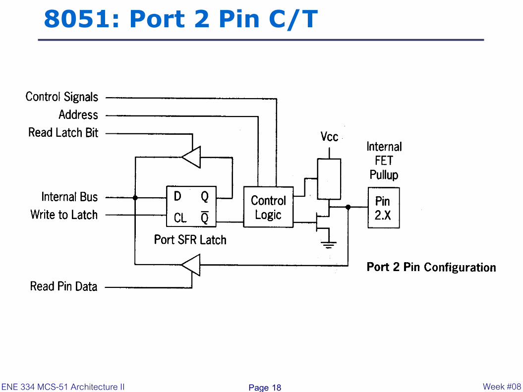
Each port has a D-type output Latch for each pin. The SFR
for each port is made up of these eight latches, which can
be addressed at the SFR address for that port. The port
latches should not be confused with the port pins; the data
on the latches does not have to be the same as that on the
pins.
ENE 334 MCS-51 Architecture II Week #08

8051: Port 1 Pin C/T
Page 17
Port 1 pins have no dual functions
To be used as input: the port bit latch must
contain a 1: turn off the FET
ENE 334 MCS-51 Architecture II Week #08
8051: Port 2 Pin C/T
Page 18 ENE 334 MCS-51 Architecture II Week #08

8051: Port 3 Pin C/T
Page 19 ENE 334 MCS-51 Architecture II Week #08

8051: Port 0 Pin C/T
Page 20
Port 0 pins may serve as inputs, outputs, or, when used
together, as a bi-directional low-order address and data
bus for external memory (time-multiplexed).
Note: External pullup resistors will be needed to
supply a logic high when using port 0 as an output (open
drain output).
ENE 334 MCS-51 Architecture II Week #08

8051: Port 0 Pin C/T
Page 21
Writing a 1 to the bit latch leaves
both output FETs off, so the pin floats.
ENE 334 MCS-51 Architecture II Week #08

8051: Port 3
Page 22 ENE 334 MCS-51 Architecture II Week #08

8051: Read-Modify-Write
Page 23
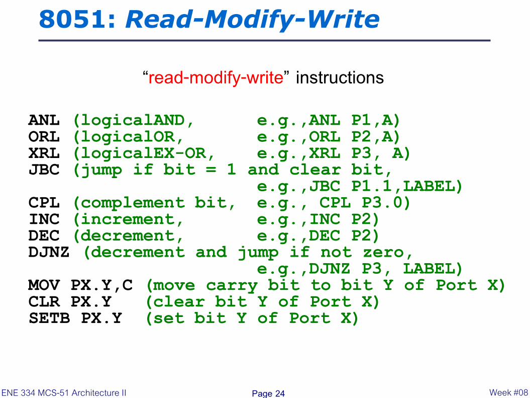
Some instructions that read a port read the latch and others read the pin. The instructions that read the latch rather than the pin are the ones that read a value possibly change it, and then rewrite it to the latch. These are called “read-modify-write” instructions The reason that read-modify-write instructions are directed to the latch rather than the pin is to avoid a possible misinterpretation of the voltage level at the pin.
ENE 334 MCS-51 Architecture II Week #08
8051: Read-Modify-Write
Page 24
“read-modify-write” instructions
ANL (logicalAND, e.g.,ANL P1,A) ORL (logicalOR, e.g.,ORL P2,A) XRL (logicalEX-OR, e.g.,XRL P3, A) JBC (jump if bit = 1 and clear bit, e.g.,JBC P1.1,LABEL) CPL (complement bit, e.g., CPL P3.0) INC (increment, e.g.,INC P2) DEC (decrement, e.g.,DEC P2) DJNZ (decrement and jump if not zero, e.g.,DJNZ P3, LABEL) MOV PX.Y,C (move carry bit to bit Y of Port X) CLR PX.Y (clear bit Y of Port X) SETB PX.Y (set bit Y of Port X)
ENE 334 MCS-51 Architecture II Week #08
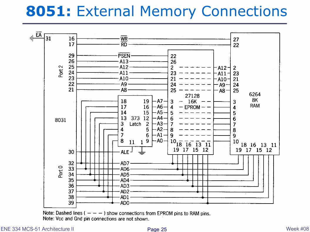
8051: External Memory Connections
Page 25 ENE 334 MCS-51 Architecture II Week #08

8051: External Memory Timing
Page 26 ENE 334 MCS-51 Architecture II Week #08
8051: Accessing External Memory
Page 27
Fetches from external Program Memory always use a 16-bit address. Accesses to external Data Memory can use either a 16-bit address (MOVX @DPTR) or an 8-bit address (MOVX @Ri). If an 8-bit address is being used (MOVX @Ri), the contents of the Port 2 SFR remain at the Port 2 pins throughout the external memory cycle.This will facilitate paging.
ENE 334 MCS-51 Architecture II Week #08
8051: Counters and Timers
Page 28
Many microcontroller applications require the counting of external events, such as the frequency of a pulse train, or the generation of precise internal time delays between computer actions. Both of these tasks can be accomplished using software techniques, but software loops for counting or timing keep the processor occupied so that other, perhaps more important, functions are not done.
ENE 334 MCS-51 Architecture II Week #08

8051: Counters and Timers
Page 29
To relieve the processor of this burden, two 16-bit up
counters, named T0 and T1, are provided for the general
use of the programmer. Each counter may be
programmed to count internal clock pulses, acting as a
timer, or programmed to count external pulses as a
counter.
ENE 334 MCS-51 Architecture II Week #08

8051: Counters and Timers
Page 30
In the “Timer” function, the register is incremented
every machine cycle.Thus one can think of it as counting
machine cycles.Since a machine cycle consists of 12
oscillator periods,the count rate is 1/12 of the oscillator
frequency.
ENE 334 MCS-51 Architecture II Week #08

8051: Counters and Timers
Page 31
In the “Counter” function, the register is incremented in response to a 1-to-0 transition at its corresponding external input pin, T0 or T1. In this function, the external input is sampled during S5P2 of every machine cycle. When the samples show a high in one cycle and a low in the next cycle, the count is incremented. The new count value appears in the register during S3P1 of the cycle following the one in which the transition was detected. Since it takes 2 machine cycles (24 oscillator periods)to recognize a 1-to-0 transition, the maximum count rate is 1/24 of the osciliator frequency.
ENE 334 MCS-51 Architecture II Week #08
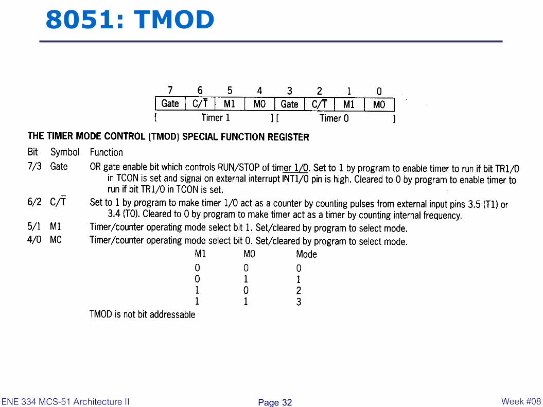
8051: TMOD
Page 32 ENE 334 MCS-51 Architecture II Week #08

8051: TCON
Page 33 ENE 334 MCS-51 Architecture II Week #08

8051: Timer/Counter Control Logic
Page 34 ENE 334 MCS-51 Architecture II Week #08
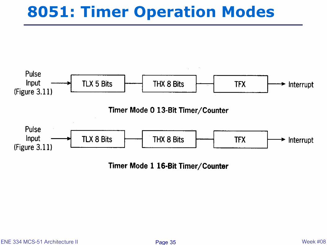
8051: Timer Operation Modes
Page 35 ENE 334 MCS-51 Architecture II Week #08

8051: Mode 0
Page 36
Either Timer in Mode 0 is an 8-bit Counter with a divide-by-32 prescaler. In this mode, the Timer register is configured as a 13-Bit register. As the count rolls over from all 1s to all 0s, it sets the Timer interrupt flag TFx. The counted input is enabled to the Timer when TRx = 1 and either GATE =0 or INTx = 1. Ex: Clock 6MHz. frequency = (6 MHz)/(12*2^5) input to THX = 15625 Hz. Interrupt freq. = (6 Mhz)/(12*2^13) 0.016384 s.
ENE 334 MCS-51 Architecture II Week #08

8051: Mode 1
Page 37
Mode 1 is the same as Mode 0, except that the Timer
register is being run with all 16 bits.
Ex: Clock 6MHz. frequency input to THX = (6 MHz)/(12*2^8)
Interrupt freq. = (6 Mhz)/(12*2^16) 0.131072 s.
ENE 334 MCS-51 Architecture II Week #08

8051: Timer Operation Modes
Page 38 ENE 334 MCS-51 Architecture II Week #08

8051: Mode 2
Page 39
Mode 2 configures theTimer register as an 8-bit Counter (TLx) with automatic reload. Overflow from TLx not only sets TFx, but also reloads TLx with the contents of THx, which is preset by software. The reload leave THx unchanged.
Ex: Placing 9Ch in THX: Count up = 100-9C = 64h = 100d Interrupt freq. = (100*12)/(6 Mhz) = 0.0002 s.
ENE 334 MCS-51 Architecture II Week #08

8051: Mode 3
Page 40
Timer 1 in Mode 3 simply holds its count.The effect is
the same as setting TR1 = 0.
Timer 0 in Mode 3 establishes TL0 and TH0 as two
separate counters. Timer 1 may still be used in mode 0, 1
or 2, while timer 0 is in mode 3 (no interrupt; can be used
for baud rate generation for the serial port,...).
ENE 334 MCS-51 Architecture II Week #08

8051: Serial Data I/O
Page 41
The 8051 has a serial data communication circuit that uses
register SBUF to hold data. Register SCON controls data
communication, register PCON controls data rates, and pins
RXD (P3.0) and TXD (P3.1) connect to the serial data
network.
ENE 334 MCS-51 Architecture II Week #08
8051: Serial Data I/O
Page 42
There are four programmable modes for serial data
communication that are chosen by setting the SMX bits in
SCON. Baud rates are determined by the mode chosen.
Figure shows the bit assignments for SCON and PCON.
ENE 334 MCS-51 Architecture II Week #08

8051: SCON
Page 43 ENE 334 MCS-51 Architecture II Week #08

8051: PCON
Page 44 ENE 334 MCS-51 Architecture II Week #08

8051: Serial Data Interrupt
Page 45
Serial data communication is a relatively slow process, occupying many milliseconds per data byte to accomplish. In order not to tie up valuable processor time, Serial Data flags are included in SCON to aid in efficient data transmission and reception. Notice that data transmission is under the complete control of the program, but reception of data is unpredictable and at random times that are beyond the control of the program.
ENE 334 MCS-51 Architecture II Week #08

8051: Serial Data Interrupt
Page 46
The serial data flags in SCON, TI and RI, are set whenever a data byte is transmitted (TI) or received (RI). These flags are ORed together to produce an interrupt to the program. The program must read these flags to determine which caused the interrupt and then clear the flag. This is unlike the timer flags that are cleared automatically; it is the responsibility of the programmer to write routines that handle the serial data flags.
ENE 334 MCS-51 Architecture II Week #08

8051: Data Transmission
Page 47
Transmission of serial data bits begins anytime data is written to SBUF. TI is set to a 1 when the data has been transmitted and signifies that SBUF is empty (for transmission purposes) and that another data byte can be sent. If the program fails to wait for the TI flag and overwrites SBUF while a previous data byte is in the process of being transmitted, the results will be unpredictable (a polite term for “garbage out”).
ENE 334 MCS-51 Architecture II Week #08
8051: Data Reception
Page 48
Reception of serial data will begin if the receive enable bit (REN) in SCON is set to 1 for all modes. In addition, for mode 0 only, RI must be cleared to 0. Receiver Interrupt flag RI is set after data has been received in all modes. Set-ting REN is the only direct program control that limits the reception of unexpected data; the requirement that RI also be 0 for mode 0 prevents the reception of new data until the program has deal with the old data and reset RI.
ENE 334 MCS-51 Architecture II Week #08

8051: Data Reception
Page 49
Reception can begin in modes 1, 2, and 3 if RI is set when
the serial stream of bits begins. RI must have been reset by
the program before the last bit is received or the incoming
data will be lost. Incoming data is not transferred to SBUF
until the last data bit has been received so that the previous
transmission can be read from SBUF while new data is
being received..
ENE 334 MCS-51 Architecture II Week #08

8051: Serial Data Mode
Page 50
- Mode 0 : Shift Register Mode
- Mode 1 : Standard UART
- Mode 2 : Multiprocessor Mode
- Mode 3 : Multiprocessor with variable Baud rate
ENE 334 MCS-51 Architecture II Week #08

8051: Shift Register Mode 0 Timing
Page 51 ENE 334 MCS-51 Architecture II Week #08

8051: Serial Data Mode 0
Page 52
SBUF to receive or transmit eight data bits using pin RXD for both functions. Pin TXD is connected to the internal shift frequency pulse source to supply shift pulses to external circuits. The shift frequency, or baud rate, is fixed at 1/12 of the oscillator frequency, the same rate used by the timers when in the timer configuration. The TXD shift clock is a square wave that is low for machine cycle states S3—S4—S5 and high for S6—S1—S2.
ENE 334 MCS-51 Architecture II Week #08

8051: Serial Data Mode 0
Page 53
When transmitting, data is shifted out of RXD; the data
changes on the falling edge of S6P2, or one clock pulse
after the rising edge of the output TXD shift clock. The
system designer must design the external circuitry that
receives this transmitted data to receive the data reliably
based on this timing.
ENE 334 MCS-51 Architecture II Week #08

8051: Serial Data Mode 0
Page 54
Received data comes in on pin RXD and should be
synchronized with the shift clock produced at TXD. Data
is sampled on the falling edge of S5P2 and shifted in to
SBUF on the rising edge of the shift clock.
ENE 334 MCS-51 Architecture II Week #08

8051: Serial Data Mode 0
Page 55
Mode 0 is intended not for data communication between computers, but as a high-speed serial data collection method using discrete logic to achieve high data rates. The baud rate used in mode 0 will be much higher than standard for any reasonable oscillator frequency; for a 6 megahertz crystal, the shift rate will be 500 kilohertz.
ENE 334 MCS-51 Architecture II Week #08
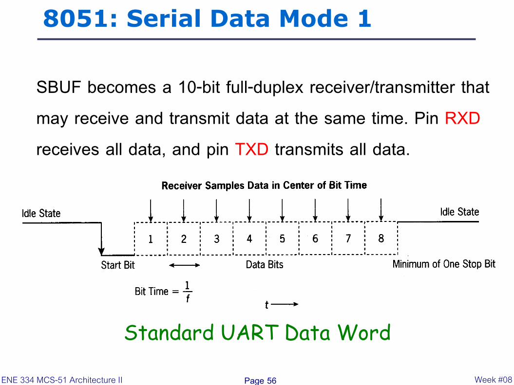
8051: Serial Data Mode 1
Page 56
SBUF becomes a 10-bit full-duplex receiver/transmitter that may receive and transmit data at the same time. Pin RXD receives all data, and pin TXD transmits all data.
Standard UART Data Word
ENE 334 MCS-51 Architecture II Week #08
8051: Serial Data Mode 1
Page 57
Transmitted data is sent as a start bit, eight data bits
(least significant bit, LSB, first), and a stop bit. Interrupt
flag TI is set once all ten bits have been sent. Each bit
interval is the inverse of the baud rate frequency, and
each bit is maintained high or low over that interval.
ENE 334 MCS-51 Architecture II Week #08

8051: Serial Data Mode 1
Page 58
Received data is obtained in the same order; reception
is triggered by the falling edge of the start bit and
continues if the stop bit is true (0 level) halfway through
the start bit interval. This is an anti-noise measure; if
the reception circuit is triggered by noise on the
transmission line, the check for a low after half a bit
interval should limit false data reception. ENE 334 MCS-51 Architecture II Week #08
8051: Serial Data Mode 1
Page 59
Data bits are shifted into the receiver at the programmed baud rate, and the data word will be loaded to SBUF if the following conditions are true: RI must be 0, and mode bit SM2 is 0 or the stop bit is 1 (the normal state of stop bits). RI set to 0 implies that the program has read the previous data byte and is ready to receive the next; a normal stop bit will then complete the transfer of data to SBUF regardless of the state of SM2.
ENE 334 MCS-51 Architecture II Week #08

8051: Serial Data Mode 1
Page 60
SM2 set to 0 enables the reception of a byte with any stop bit state, a condition that is of limited use in this mode, but very useful in modes 2 and 3. SM2 set to 1 forces reception of only “good” stop bits, an anti-noise safeguard. Of the original ten bits the start bit is discarded, the eight data bits go to SBUF, and the stop bit is saved in bit RB8 of SCON. RI is set to 1 indicating a new data byte has been received.
ENE 334 MCS-51 Architecture II Week #08

8051: Serial Data Mode 1
Page 61
If RI is found to be set at the end of the reception,
indicating that the previously received data byte has not
been read by the program, or if the other conditions
listed are not true, the new data will not be loaded and
will be lost.
ENE 334 MCS-51 Architecture II Week #08

8051: Mode 1 BAUD Rates
Page 62
Timer 1 is used to generate the baud rate for mode 1 by using the Overflow flag of the timer to determine the baud frequency. Typically, timer 1 is used in timer mode 2 as an autoload 8-bit timer that generates the baud frequency:
SMOD is the control bit in PCON
ENE 334 MCS-51 Architecture II Week #08

8051: Mode 1 BAUD Rates
Page 63
If timer 1 is not run in timer mode 2, then the baud rate is:
and timer 1 can be run using the internal clock or as a counter that receives clock pulses from any external source via pin T1.
ENE 334 MCS-51 Architecture II Week #08

8051: Mode 1 BAUD Rates Ex:
Page 64
The oscillator frequency is chosen to help generate both
standard and nonstandard baud rates. If standard baud
rates are desired, then an 11.0592 megahertz crystal
could be selected. To get a standard rate of 9600 hertz
then, the setting of TH1 may be found as follows:
ENE 334 MCS-51 Architecture II Week #08

8051: Mode 1 BAUD Rates Note:
Page 65
if SMOD is cleared to 0. Note that the frequency that is generated by the timer is 16 (SMOD = 0) or 32 (SMOD = 1) times the actual serial data communication rate. The UART must be fed a clock frequency that is much higher than the serial baud rate in order to be able to sample close to the center of each received bit. Clearly, a UART clock rate equal to the baud rate would not be “fine” enough to slice each serial bit into pieces.
ENE 334 MCS-51 Architecture II Week #08

8051: Serial Data Mode 2
Page 66
Mode 2 is similar to mode 1 except 11 bits are
transmitted: a start bit, nine data bits, and a stop bit.
The ninth data bit is copied from bit TB8 in SCON
during transmit and stored in bit RB8 of SCON when
data is received. Both the start and stop bits are
discarded.
ENE 334 MCS-51 Architecture II Week #08

8051: Mode 2 BAUD Rate
Page 67
The baud rate is programmed as follows:
Multiprocessor Data Word
ENE 334 MCS-51 Architecture II Week #08

8051: Mode 2 - Multiprocessor
Page 68
The conditions for setting RI for mode 2 are similar to mode 1: RI must be 0 before the last bit is received, and SM2 must be 0 or the ninth data bit must be a 1. Setting RI based on the state of SM2 in the receiving 8051 and the state of bit 9 in the transmitted message makes multiprocessing possible by enabling some receivers to be interrupted by certain messages, while other receivers ignore those messages.
ENE 334 MCS-51 Architecture II Week #08

8051: Mode 2 - Multiprocessor
Page 69
Only those 8051s that have SM2 set to 0 will be interrupted by received data that has the ninth data bit set to 0; those with SM2 set to 1 will not be interrupted by messages with data bit 9 at 0. All receivers will be interrupted by data words that have the ninth data bit set to 1; the state of SM2 will not block reception of such messages.
ENE 334 MCS-51 Architecture II Week #08
8051: Mode 2 - Multiprocessor
Page 70
This scheme allows the transmitting computer to “talk” to selected receiving computers without interrupting other receiving computers. Receiving computers can be commanded by the “talker” to “listen” or “deafen” by transmitting coded byte(s) with the ninth data bit set to 1. The 1 in data bit 9 interrupts all receivers, instructing those that are programmed to respond to the coded byte(s) to program the state of SM2 in their respective SCON registers.
ENE 334 MCS-51 Architecture II Week #08
8051: Mode 2 - Multiprocessor
Page 71
Selected listeners then respond to the bit 9 set to 0 messages, while all other receivers ignore these messages. The talker can change the mix of listeners by transmitting bit 9 set to 1 messages that instruct new listeners to set SM2 to 0, while others are instructed to set SM2 to 1.
ENE 334 MCS-51 Architecture II Week #08

8051: Serial Data Mode 3
Page 72
Mode 3 is identical to mode 2 except that the baud
rate is determined exactly as in mode 1, using timer 1
to generate communication frequencies.
ENE 334 MCS-51 Architecture II Week #08

8051: Interrupts
Page 73
A computer program has only two ways to determine
the conditions that exist in internal and external circuits.
One method uses software instructions that jump to
subroutines on the states of flags and port pins. The
second method responds to hardware signals, called
interrupts that force the program to call a subroutine.
ENE 334 MCS-51 Architecture II Week #08

8051: Interrupts
Page 74
Software techniques use up processor time that could be devoted to other tasks; interrupts take processor time only when action by the program is needed. Most applications of microcontrollers involve responding to events quickly enough to control the environment that generates the events (generically termed real-time programming). Interrupts are often the only way in which real-time programming can be done successfully.
ENE 334 MCS-51 Architecture II Week #08

8051: Interrupts
Page 75
Interrupts may be generated by internal chip
operations or provided by external sources. Any
interrupt can cause the 8051 to perform a hardware call
to an interrupt-handling subroutine that is located at a
predetermined (by the 8051 designers) absolute
address in program memory.
ENE 334 MCS-51 Architecture II Week #08
8051: Interrupts
Page 76
Five interrupts are provided in the 8051. Three of
these are generated automatically by internal
operations: Timer flag 0 (TF0), Timer flag 1 (TF1), and
the serial port interrupt (RI or TI). Two interrupts are
triggered by external signals provided by circuitry that is
connected to port pins P3.2 and P3.3.
ENE 334 MCS-51 Architecture II Week #08
8051: Interrupts
Page 77
All interrupt functions are under the control of the
program. The programmer is able to alter control bits in
the Interrupt Enable register (IE), the Interrupt Priority
register (IP), and the Timer Control register (TCON).
The program can block all or any combination of the
interrupts from acting on the program by suitably setting
or clearing bits in these registers.
ENE 334 MCS-51 Architecture II Week #08

8051: IE
Page 78 ENE 334 MCS-51 Architecture II Week #08

8051: IP
Page 79 ENE 334 MCS-51 Architecture II Week #08

8051: Interrupts
Page 80
After the interrupt has been handled by the interrupt subroutine, which is placed by the programmer at the interrupt location in program memory, the interrupted program must resume operation at the instruction where the interrupt took place. Program resumption is done by storing the interrupted PC address on the stack in RAM before changing the PC to the interrupt address in ROM. The PC address will be restored from the stack after an RETI instruction is executed at the end of the interrupt subroutine.
ENE 334 MCS-51 Architecture II Week #08
8051: Timer Flag Interrupts
Page 81
When a timer/counter overflows, the corresponding
Timer flag, TF0 or TF1, is set to 1. The flag is cleared
to 0 when the resulting interrupt generates a program
call to the appropriate timer subroutine in memory.
ENE 334 MCS-51 Architecture II Week #08
8051: Serial Port Interrupts
Page 82
If a data byte is received, an interrupt bit, RI, is set to 1 in the SCON register. When a data byte has been transmitted an interrupt bit, TI, is set in SCON. These are ORed together to provide a single interrupt to the processor: the serial port interrupt. These bits are not cleared when the interrupt-generated program call is made by the processor. The program that handles serial data communication must reset RI or TI to 0 to enable the next data communication operation.
ENE 334 MCS-51 Architecture II Week #08

8051: External Interrupts
Page 83
the Interrupt flags lE0 and IE1 in the TCON register can be set to 1 by two different methods. The IEX flags may be set when the INTX pin signal reaches a low level, or the flags may be set when a high-to-low transition takes place on the INTX pin. Bits IT0 and IT1 in TCON program the pins for low-level interrupt when set to 0 and program the pins for transition interrupt when set to 1.
ENE 334 MCS-51 Architecture II Week #08

8051: External Interrupts
Page 84
Flags IEX will be reset when a transition-generated interrupt is accepted by the processor and the interrupt subroutine is accessed. It is the responsibility of the system designer and programmer to reset any level-generated external interrupts when they are serviced by the program. The external circuit must remove the low level before an RETI is executed. Failure to remove the low will result in an immediate interrupt after RETI, from the same source.
ENE 334 MCS-51 Architecture II Week #08

8051: Reset
Page 85
A reset can be considered to be the ultimate interrupt because the program may not block the action of the voltage on the RST pin. This type of interrupt is often called nonmaskable, because no combination of bits in any register can stop, or mask, the reset action. Unlike other interrupts, the PC is not stored for later program resumption; a reset is an absolute command to jump to program address 0000h and commence running from there.
ENE 334 MCS-51 Architecture II Week #08
8051: Reset
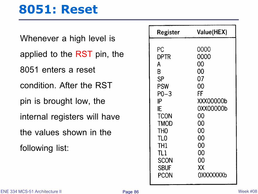
Page 86
Whenever a high level is applied to the RST pin, the 8051 enters a reset condition. After the RST pin is brought low, the internal registers will have the values shown in the following list:
ENE 334 MCS-51 Architecture II Week #08

8051: Interrupt Priority
Page 87
Register IP bits determine if any interrupt is to have a
high or low priority. Bits set to 1 give the accompanying
interrupt a high priority; a 0 assigns a low priority.
Interrupts with a high priority can interrupt another
interrupt with a lower priority; the lower priority interrupt
continues after the higher is finished.
ENE 334 MCS-51 Architecture II Week #08
8051: Interrupt Priority
Page 88
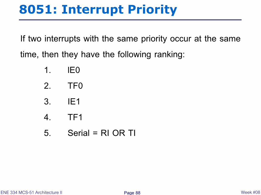
If two interrupts with the same priority occur at the same time, then they have the following ranking: 1. lE0 2. TF0 3. IE1 4. TF1 5. Serial = RI OR TI
ENE 334 MCS-51 Architecture II Week #08
8051: Interrupt Destinations
Page 89
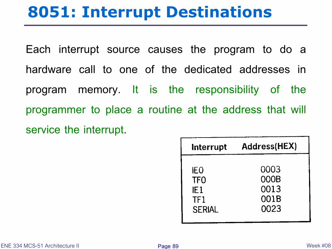
Each interrupt source causes the program to do a hardware call to one of the dedicated addresses in program memory. It is the responsibility of the programmer to place a routine at the address that will service the interrupt.
ENE 334 MCS-51 Architecture II Week #08

8051: Summary
Page 90 ENE 334 MCS-51 Architecture II Week #08

8051: Summary
Page 91 ENE 334 MCS-51 Architecture II Week #08
Hw:
Page 92 ENE 334 MCS-51 Architecture II Week #08


