Int. Journal of Electrical & Electronics Engg. Vol. 2, Spl. Issue 1 (2015) e-ISSN: 1694-2310 | p-ISSN: 1694-2426 NITTTR, Chandigarh EDIT -2015 104 Energy Efficient Design of Multiplexer Using Adiabatic logic 1 Richa Singh, 2 Prateek Raj Gautam, 3 Anjali Sharma 1,2 Dept.of Electronics& Communication, Allen House Institute of Technology, Rooma, Kanpur,India Dept.of Electronics & Communication, AP Goyal University, Shimla, India 1 [email protected], 2 [email protected], 3 [email protected]Abstract—the increasing prominence of portable systems and the need to limit the power consumption in very high density VLSI chips have led to rapid and innovative developments in low power design during the recent years. The CMOS technology provides circuits with very low static power dissipation, during the switching operation currents are generated, due to the discharge of load capacitances that cause power dissipation increasing with the clock frequency. The adiabatic technique prevents such losses, the charge does not flow from the supply voltage to the load capacitance and then to ground, but it flows back to a trapezoidal or sinusoidal supply voltage and can be reused.In this paper a low 2:1 multiplexer is designed using positive feedback adiabatic logic. The design is simulated at .12μm technology using Microwind 3.1. Simulated results shows that proposed design saves 38% energy as compare to conventional CMOS design. Keywords- VLSI, PFAL, Adiabatic, BSIM, Multiplexer. INTRODUCTION The need for low power design is becoming a major issue in high performance digital systems, such as microprocessors, digital signal processors, and other application. The common traits of high performance chips are the high integration density and high clock frequency. The power dissipation of the chip, and thus, the temperature, increases with the increasing clock frequency. Since the dissipated heat must be removed effectively to keep the chip temperature at an acceptable level. There are many ways t achieve low power in digital circuits, it involves reduction of the switching events, decrease the node capacitance, reduce the voltage swing or apply a combination of these methods. Yet in all these methods energy drawn from the power supply is used only once before being dissipated[1]. . In CMOS logic design half of the power is dissipation in PMOS network and stored energy is dissipated during discharging process of output load capacitor during the switching events. Most of the power consumption reduction techniques are based upon scaling of the supply voltage, reducing capacitance and switching activity. Yet in all these cases, energy drawn from the power supply is used only once before being dissipated. Thus to increase the energy efficiency of logic circuits, a technique is required that can reuse the energy stored on load capacitor. It has been found that there is a fundamental relation between computation and power dissipation. That is if somehow computation could be implemented without any loss of information, then the energy required by it could be potentially reduced to zero. This can be done by performing all computation in reversible manner. Also energy dissipation depends upon average voltage drop traversed by charge that flows on to the load capacitance [2-3]. By using smaller voltage steps or increments dissipation can be reduced [3]. The minimum power consumption during the charge transfer phase is termed as adiabatic switching. Fig.1 Conventional CMOS logic circuit with pull-up (F) and pull-down (/F) networks ADIABATIC PRINCIPLE Most of the power saving techniques involved scaling of the power supply, which results, substantial increase in subthreshold leakage current also it causes uncertainty in the process variation. Therefore some other technique is required which is independent of voltage scaling. It has been found that there is fundamental connection between computation and power dissipation. That is if somehow computation could be implemented without any loss of information, then energy required by it could be potentially reduced to zero. This can be achieved by performing all the computation in a reversible manner. Thus minimum power consumption during charge transfer phase is known as adiabatic switching [4]. In Fig. 2output load capacitance is charged by a constant current source instead of a constant voltage source used in conventional CMOS structures. This circuit is same as the equivalent model used in charging process in conventional CMOS. On resistance of pull up PMOS network is represented by R and C 0 is the output capacitance. It is noted that constant charging current corresponds to a linear voltage ramp. Energy dissipated through adiabatic logic is given as [5-6]
Abstract—the increasing prominence of portable systems andthe need to limit the power consumption in very high densityVLSI chips have led to rapid and innovative developments inlow power design during the recent years. The CMOStechnology provides circuits with very low static powerdissipation, during the switching operation currents aregenerated, due to the discharge of load capacitances thatcause power dissipation increasing with the clock frequency.The adiabatic technique prevents such losses, the charge doesnot flow from the supply voltage to the load capacitance andthen to ground, but it flows back to a trapezoidal orsinusoidal supply voltage and can be reused.In this paper alow 2:1 multiplexer is designed using positive feedbackadiabatic logic. The design is simulated at .12µm technologyusing Microwind 3.1. Simulated results shows that proposeddesign saves 38% energy as compare to conventional CMOSdesign.
INTRODUCTIONThe need for low power design is becoming a major issuein high performance digital systems, such asmicroprocessors, digital signal processors, and otherapplication. The common traits of high performance chipsare the high integration density and high clock frequency.The power dissipation of the chip, and thus, thetemperature, increases with the increasing clock frequency.Since the dissipated heat must be removed effectively tokeep the chip temperature at an acceptable level. There aremany ways t achieve low power in digital circuits, itinvolves reduction of the switching events, decrease thenode capacitance, reduce the voltage swing or apply acombination of these methods. Yet in all these methodsenergy drawn from the power supply is used only oncebefore being dissipated[1]..In CMOS logic design half of the power is dissipation inPMOS network and stored energy is dissipated duringdischarging process of output load capacitor during theswitching events. Most of the power consumptionreduction techniques are based upon scaling of the supplyvoltage, reducing capacitance and switching activity. Yetin all these cases, energy drawn from the power supply isused only once before being dissipated. Thus to increasethe energy efficiency of logic circuits, a technique isrequired that can reuse the energy stored on load capacitor.It has been found that there is a fundamental relationbetween computation and power dissipation. That is ifsomehow computation could be implemented without anyloss of information, then the energy required by it could bepotentially reduced to zero. This can be done byperforming all computation in reversible manner. Alsoenergy dissipation depends upon average voltage drop
traversed by charge that flows on to the load capacitance[2-3]. By using smaller voltage steps or incrementsdissipation can be reduced [3]. The minimum powerconsumption during the charge transfer phase is termed asadiabatic switching.
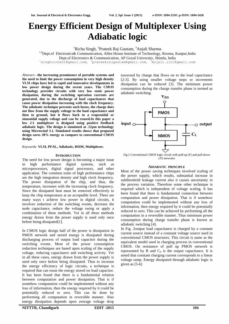
Fig.1 Conventional CMOS logic circuit with pull-up (F) and pull-down(/F) networks
ADIABATIC PRINCIPLEMost of the power saving techniques involved scaling ofthe power supply, which results, substantial increase insubthreshold leakage current also it causes uncertainty inthe process variation. Therefore some other technique isrequired which is independent of voltage scaling. It hasbeen found that there is fundamental connection betweencomputation and power dissipation. That is if somehowcomputation could be implemented without any loss ofinformation, then energy required by it could be potentiallyreduced to zero. This can be achieved by performing all thecomputation in a reversible manner. Thus minimum powerconsumption during charge transfer phase is known asadiabatic switching [4].In Fig. 2output load capacitance is charged by a constantcurrent source instead of a constant voltage source used inconventional CMOS structures. This circuit is same as theequivalent model used in charging process in conventionalCMOS. On resistance of pull up PMOS network isrepresented by R and C0 is the output capacitance. It isnoted that constant charging current corresponds to a linearvoltage ramp. Energy dissipated through adiabatic logic isgiven as [5-6]
Fig.2 Equivalent model during charging phase in adiabatic circuits [4]
It can be seen from equation from equation 1 that Ifcharging period T is larger than 2RC then dissipatedenergy can be made smaller than Conventional CMOScircuit. Thus dissipated energy can be made arbitrarilysmall by increasing the charging period. Hence by usingconstant current source energy can be transferred fromsupply to load capacitor with any dissipation and theenergy stored on the load capacitance after chargingprocess send back to the supply voltage by simplyreversing the direction of current source. Thus recycling isvery attractive feature in adiabatic logic. The constantcurrent supply must be capable of retrieving the chargeback to the power supply as shown in fig. 2. Adiabaticcircuits does not use standard power supply instead of thisit uses pulsating power supply which is also called aspulsed power supply[7-8].
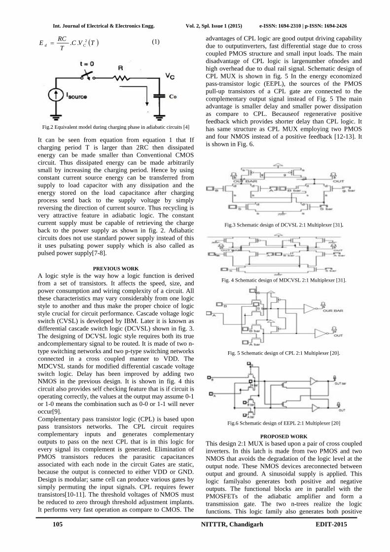
PREVIOUS WORKA logic style is the way how a logic function is derivedfrom a set of transistors. It affects the speed, size, andpower consumption and wiring complexity of a circuit. Allthese characteristics may vary considerably from one logicstyle to another and thus make the proper choice of logicstyle crucial for circuit performance. Cascade voltage logicswitch (CVSL) is developed by IBM. Later it is known asdifferential cascade switch logic (DCVSL) shown in fig. 3.The designing of DCVSL logic style requires both its trueandcomplementary signal to be routed. It is made of two n-type switching networks and two p-type switching networksconnected in a cross coupled manner to VDD. TheMDCVSL stands for modified differential cascade voltageswitch logic. Delay has been improved by adding twoNMOS in the previous design. It is shown in fig. 4 thiscircuit also provides self checking feature that is if circuit isoperating correctly, the values at the output may assume 0-1or 1-0 means the combination such as 0-0 or 1-1 will neveroccur[9].Complementary pass transistor logic (CPL) is based uponpass transistors networks. The CPL circuit requirescomplementary inputs and generates complementaryoutputs to pass on the next CPL that is in this logic forevery signal its complement is generated. Elimination ofPMOS transistors reduces the parasitic capacitancesassociated with each node in the circuit Gates are static,because the output is connected to either VDD or GND.Design is modular; same cell can produce various gates bysimply permuting the input signals. CPL requires fewertransistors[10-11]. The threshold voltages of NMOS mustbe reduced to zero through threshold adjustment implants.It performs very fast operation as compare to CMOS. The
advantages of CPL logic are good output driving capabilitydue to outputinverters, fast differential stage due to crosscoupled PMOS structure and small input loads. The maindisadvantage of CPL logic is largenumber ofnodes andhigh overhead due to dual rail signal. Schematic design ofCPL MUX is shown in fig. 5 In the energy economizedpass-transistor logic (EEPL), the sources of the PMOSpull-up transistors of a CPL gate are connected to thecomplementary output signal instead of Fig. 5 The mainadvantage is smaller delay and smaller power dissipationas compare to CPL. Becauseof regenerative positivefeedback which provides shorter delay than CPL logic. Ithas same structure as CPL MUX employing two PMOSand four NMOS instead of a positive feedback [12-13]. Itis shown in Fig. 6.
Fig.3 Schematic design of DCVSL 2:1 Multiplexer [31].
Fig. 4 Schematic design of MDCVSL 2:1 Multiplexer [31].
Fig. 5 Schematic design of CPL 2:1 Multiplexer [20].
Fig.6 Schematic design of EEPL 2:1 Multiplexer [20]
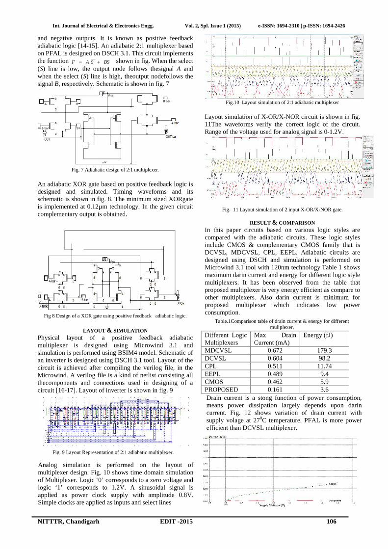
PROPOSED WORKThis design 2:1 MUX is based upon a pair of cross coupledinverters. In this latch is made from two PMOS and twoNMOS that avoids the degradation of the logic level at theoutput node. These NMOS devices areconnected betweenoutput and ground. A sinusoidal supply is applied. Thislogic familyalso generates both positive and negativeoutputs. The functional blocks are in parallel with thePMOSFETs of the adiabatic amplifier and form atransmission gate. The two n-trees realize the logicfunctions. This logic family also generates both positive
and negative outputs. It is known as positive feedbackadiabatic logic [14-15]. An adiabatic 2:1 multiplexer basedon PFAL is designed on DSCH 3.1. This circuit implementsthe function BSSAF shown in fig. When the select(S) line is low, the output node follows thesignal A andwhen the select (S) line is high, theoutput nodefollows thesignal B, respectively. Schematic is shown in fig. 7
Fig. 7 Adiabatic design of 2:1 multiplexer.
An adiabatic XOR gate based on positive feedback logic isdesigned and simulated. Timing waveforms and itsschematic is shown in fig. 8. The minimum sized XORgateis implemented at 0.12µm technology. In the given circuitcomplementary output is obtained.
Fig 8 Design of a XOR gate using positive feedback adiabatic logic.
LAYOUT & SIMULATIONPhysical layout of a positive feedback adiabaticmultiplexer is designed using Microwind 3.1 andsimulation is performed using BSIM4 model. Schematic ofan inverter is designed using DSCH 3.1 tool. Layout of thecircuit is achieved after compiling the verilog file, in theMicrowind. A verilog file is a kind of netlist consisting allthecomponents and connections used in designing of acircuit [16-17]. Layout of inverter is shown in fig. 9
Fig.10 Layout simulation of 2:1 adiabatic multiplexer
Layout simulation of X-OR/X-NOR circuit is shown in fig.11The waveforms verify the correct logic of the circuit.Range of the voltage used for analog signal is 0-1.2V.
Fig. 11 Layout simulation of 2 input X-OR/X-NOR gate.
RESULT & COMPARISONIn this paper circuits based on various logic styles arecompared with the adiabatic circuits. These logic stylesinclude CMOS & complementary CMOS family that isDCVSL, MDCVSL, CPL, EEPL. Adiabatic circuits aredesigned using DSCH and simulation is performed onMicrowind 3.1 tool with 120nm technology.Table 1 showsmaximum darin current and energy for different logic stylemultiplexers. It has been observed from the table thatproposed multiplexer is very energy efficient as compare toother multiplexers. Also darin current is minimum forproposed multiplexer which indicates low powerconsumption.
Table.1Comparison table of drain current & energy for differentmuliplexer,
Analog simulation is performed on the layout ofmultiplexer design. Fig. 10 shows time domain simulationof Multiplexer. Logic ‘0’ corresponds to a zero voltage andlogic ‘1’ corresponds to 1.2V. A sinusoidal signal isapplied as power clock supply with amplitude 0.8V.Simple clocks are applied as inputs and select lines
Fig. 9 Layout Representation of 2:1 adiabatic multiplexer.
Drain current is a stong function of power consumption,means power dissipation largely depends upon darincurrent. Fig. 12 shows variation of drain current withsupply volage at 270C temperature. PFAL is more powerefficient than DCVSL multiplexer.
CONLUSIONMultiplexer through various logic style has been designedand simulated using DSCH & Microwind 3.1. These logicstyles includes DVCSL, MDCVSL, CPL and EEPLmultiplexer design. It is observed that proposedMultiplexer shows better performance in terms of powerconsumption. It is recorded that 49.56% and 68.32%improvement is obtained in terms power consumption ascompare toCMOS It has been observed that proposedmultiplexer saves 38.9% energy as compare to CMOSmultiplexer. All results are verified at different supplyvoltage and temperature. Proposed Multiplexer showsgood performance with supply voltage vs temperature &supply voltage vs drain current variations as compare toEEPL, CPL, DCVSL, MDCVSL multiplexer.energy ascompare to CMOS multiplexer. All results are verified atdifferent supply voltage and temperature. ProposedMultiplexer shows good performance with supply voltagevs temperature &supply voltage vs drain current variationsas compare to EEPL, CPL, DCVSL, MDCVSLmultiplexer
REFERENCES1) ....Sung-Mo Kang, Yusuf Leblebici, CMOS DigitalIntegrated Circuits:
Analysis and Design TATA McGRAW-HILL, pp. 197-519.2) ....N. Weste and K. Eshraghian, Principles of CMOS VLSI Design: A
System Perspective reading pearson education, Addision-Wesleypp. 145-148.
3) H. J. M. Veendrick, “Short-circuit Dissipation of Static CMOSCircuitry and its Impact on the Design of Buffer Circuits,” IEEEJournal of Solid State Circuits, pp. 468-473thinfilmsandexchangeanisotropy,”inMagnetism,vol.III,G.T.RadoandH.Suhl,Eds.NewYork:Academic,1963,, August 1984.
4) I.S.JacobsandC.P.Bean, “Fineparticles,pp.271–350.A. P. Chandrakasan and R. W. Brodersen, Low-power CMOS digital
of multiplexer based Compressor Using Adiabatic Logic,”
International Journal of Computer Applications, pp. 45-50, Vol. 81,November 2013..
6) Richa Singh, Rajesh Mehra, “Power Efficient Design of MultiplexerUsing Adiabatic Logic,” International Journal of Advances inEngineering & Technology, pp. 246-254, Vol. 6, March 2013. M.Young, TheTechnical Writer's Handbook. Mill Valley, CA:University Science, 1989.
7) Richa Singh, Rajesh Mehra, “Power Efficient Design of MultiplexerUsing Adiabatic Logic,” International Journal of Advances inEngineering & Technology, pp. 246-254, Vol. 6,
8) March 2013. M. Young, TheTechnical Writer's Handbook. MillValley, CA: University Science, 1989.
A. P. Chandrakasan and R. W. Brodersen, Low-power CMOS digitaldesign, Kluwer Academic, Norwell, Ma, pp. 45-89, 1995.
9) Varga, L.Kovacs, F. Hosszu, G. “An Improved Pass-Gate Adiabatic Logic,” IEEEConference on Application SpecificIntegrated chip, pp. 208-211, 2001
10) Yingtao Jiang, Al-Sheraidah, Yuke Wang, Edwin Sha and Jin-GyunChung, “A Novel Multiplexer-Based Low-Power Full Adder,” IEEETransactions on Circuit and Systems-2nd:Express Brief, Vol. 51, pp.345-348, July 2004.
11) Suhwan Kim, Ziesler, Conrad H. Ziesler and Marios C.Papaefthymiou, “Charge-Recovery Computing on Silicon,” IEEETransactions on Computers, Vol. 54, pp. 651-659, June 2005.
12) Hsu-Wei Huang, Cheng-Yeh Wang, Jing Yang Jou, “An EfficientHeterogeneous Tree Multiplexer Synthesis Technique,” IEEETransactions on Computer-Aided design of Integrated Circuits andSystem, Vol. 24, pp. 1622-1629, October 2005.
13) Muhammad Arsalanand Maitham Shams, “Charge-Recovery PowerClock Generators for Adiabatic Logic Circuits,” IEEE Conferenceon Embedded System designs, pp. 171-174, 2005.
14) SambhuN.Pradhan, Gopal Paul, Ajit Pal, Bhargab B. Bhattacharya,“Power Aware BDD-Based Logic Synthesis Using AdiabaticMultiplexer,” IEEE Conference on Electrical and ComputerEngineering, pp. 149-152, December 2006.
15) XuJian, Wang Peng-jun, Zeng Xiao-yang, “Research of AdiabaticMultiplier Based on CTGAL,” IEEE Conference on ApplicationSpecific Integrated Chip, pp. 138-141, 2007.
16) Massimo Alioto and Gaetano Palumbo, “Design of Large Fan-InCMOS Multiplexer Accounting for Interconnects,” IEEETransactions on Circuits And Systems-2nd:Express Briefs, Vol. 54,pp. 484-488, June 2007.
Fig. 12 Power consumption vs supply voltage for CMOS and adiabaticcompressors.