XAPP522 (v1.2) October 31, 2014 www.xilinx.com 1 Summary The multiplexing of a signals is a common function that is generally handled adequately by the Xilinx® implementation tools and devices. However, there can be particularly challenging designs in which it is helpful to consider different multiplexing techniques and to select the most appropriate for the situation. A solid understanding of the device features and their suitability for implementing each multiplexing technique empowers the designer to structure designs for success. This application note also illustrates VHDL and Verilog code that ensures maximum control over the implementation yielding the most predictable results. You can download the Reference Design Files for this application note from the Xilinx website. For detailed information about the design files, see Reference Design. Introduction The FPGA is a computational and logic substrate with many concurrent switching activities. For example, in a wireline network routing system, the FPGA can have numerous wiring patterns between logic elements that are multiples of M:N. With the increasing need for high bandwidth, both M and N can be relatively large and, with M > N, this can lead to some significant multiplexing tasks having to be implemented. As a result, datapath routing across Spartan®-6 FPGAs, Virtex®-6 FPGAs, and 7 series FPGAs is a fundamental part of system design. Effort beyond synthesis is sometimes required to ensure that an FPGA implementation meets the system goals, for example using the PlanAhead™ design tool to lock down placement. As an additional approach, this application note offers system designers new techniques for efficient implementation of data routing logic that only requires HDL specification with the ISE® Design Suite or Vivado® Design Suite to work. The techniques do two things concurrently to improve design closure. First, performance is improved by compacting more logic within slices, while using less general-purpose interconnect wire. Secondly, implementation with more-logic/less-wire increases the determinism of results, impacting other aspects of system design including reduced FPGA utilization and software runtimes for implementation. The path to achieving more efficient multiplexing and data routing is first understanding features of Spartan-6 FPGAs, Virtex-6 FPGAs, and 7 series FPGAs slice architecture not normally inferred with behavioral synthesis for routing logic. From this vantage point, practical techniques that are relatively simple allow large gains in terms of reduced resources and fewer wires-per-bit of M:N logic. This design illustrates several 2 N -wide multiplexers, binary-select Application Note: Spartan-6 Family, Virtex-6 Family, 7 Series FPGAs XAPP522 (v1.2) October 31, 2014 Multiplexer Design Techniques for Datapath Performance with Minimized Routing Resources Author: Ken Chapman
Transcript
XAPP522 (v1.2) October 31, 2014 www.xilinx.com 1
SummaryThe multiplexing of a signals is a common function that is generally handled adequately by the Xilinx® implementation tools and devices. However, there can be particularly challenging designs in which it is helpful to consider different multiplexing techniques and to select the most appropriate for the situation. A solid understanding of the device features and their suitability for implementing each multiplexing technique empowers the designer to structure designs for success. This application note also illustrates VHDL and Verilog code that ensures maximum control over the implementation yielding the most predictable results.
You can download the Reference Design Files for this application note from the Xilinx website. For detailed information about the design files, see Reference Design.
IntroductionThe FPGA is a computational and logic substrate with many concurrent switching activities. For example, in a wireline network routing system, the FPGA can have numerous wiring patterns between logic elements that are multiples of M:N. With the increasing need for high bandwidth, both M and N can be relatively large and, with M > N, this can lead to some significant multiplexing tasks having to be implemented. As a result, datapath routing across Spartan®-6 FPGAs, Virtex®-6 FPGAs, and 7 series FPGAs is a fundamental part of system design.
Effort beyond synthesis is sometimes required to ensure that an FPGA implementation meets the system goals, for example using the PlanAhead™ design tool to lock down placement. As an additional approach, this application note offers system designers new techniques for eff icient implementation of data routing logic that only requires HDL specification with the ISE® Design Suite or Vivado® Design Suite to work. The techniques do two things concurrently to improve design closure. First, performance is improved by compacting more logic within slices, while using less general-purpose interconnect wire. Secondly, implementation with more-logic/less-wire increases the determinism of results, impacting other aspects of system design including reduced FPGA utilization and software runtimes for implementation.
The path to achieving more efficient multiplexing and data routing is f irst understanding features of Spartan-6 FPGAs, Virtex-6 FPGAs, and 7 series FPGAs slice architecture not normally inferred with behavioral synthesis for routing logic. From this vantage point, practical techniques that are relatively simple allow large gains in terms of reduced resources and fewer wires-per-bit of M:N logic. This design illustrates several 2N-wide multiplexers, binary-select
Application Note: Spartan-6 Family, Virtex-6 Family, 7 Series FPGAs
XAPP522 (v1.2) October 31, 2014
Multiplexer Design Techniques for Datapath Performance with Minimized Routing ResourcesAuthor: Ken Chapman
multiplexers with size other than 2N, alternative data selectors, and their implementation in FPGA. The techniques use basic elements (BELs) in the FPGA slice to form reusable cells that are easily modified for user requirements and placeable anywhere on the FPGA without user constraints.
Issues with Behavioral Synthesis of Data Routing LogicBehavioral synthesis of multiplexers and data routing logic, in conjunction with the FPGA implementation tools, sometimes result in less eff iciency than is achievable, particularly when implementing very wide multiplexers. While synthesis tools generally exploit the most obvious multiplexing features provided in the devices, the potential for inefficiency increases when larger datapath widths need to be accommodated at increasingly higher clock rates.
Larger multiplexer structures can require cascading of many instances of smaller multiplexers. Such replicated cascades tend to have many wires to link the LUTs together with general purpose interconnect. Multiplexers inherently have a many-to-few (M:N) wiring pattern. Large multiplexers dictate the need for a very large number of wires. These wires can also cross a large fraction of the FPGA because data must often be exchanged between functions such as ISERDES and OSERDES primitives, block RAM memories, and DSP blocks spatially distributed across the FPGA. Heavy utilization of routing resources between slices is a key contributor to slower AC performance so choosing an appropriate implementation style can really help.
Despite increasing pressure on the general-purpose routing resources outside the slices, some available FPGA resources are most often under utilized. These resources are all located within the slice itself. Use of these resources can be applied in structures that do more logic with less wire.
FPGA Slice Building Blocks: Looking WithinAll Spartan-6 FPGAs, Virtex-6 FPGAs, and 7 series FPGAs have numerous configurable logic blocks (CLBs) and each contains two slices. This application note exploits the features of the following slice types:
• SLICEL: Perform only logic and arithmetic functions.
• SLICEM: Perform logic, arithmetic, and memory or shift register functions.
A mix of SLICELs and SLICEMs provides a variety of system implementation capabilities. This design illustrates SLICEL only, without loss of generality, because the techniques described work equally well with SLICEM slices.
Note: Virtex-6 FPGAs and 7 series FPGAs only contain the SLICEL and SLICEM types, whereas, Spartan-6 FPGAs also contain a simplif ied SLICEX type. Although the techniques described in this application note cannot be implemented in a SLICEX, there is normally an adequate quantity of SLICEL and SLICEM available to service the requirements of a design.
There are four 6-input LUTs (LUT6) and eight flip-flops in each slice. Figure 1 shows the detailed internal logic featured within a SLICEL.
In Figure 1, additional internal BELs and other resources are highlighted in yellow, specif ic input oriented pathways are highlighted in red, and output oriented pathways are highlighted in green. All pathways in this discussion are internal to the slice and do not use any
general-purpose routing resources. The BELs and internal slice routing are also extremely fast because they were designed for fast arithmetic logic and multiplexing.
With an understanding of how these non-arithmetic building blocks work, scalable multiplexing and data routing structures can be envisioned. In addition, the flexibility of these building blocks leads to a rich set of datapath elements.
MUXF7 and MUXF8 BELsThe two MUXF7 and one MUXF8 BELs are highlighted with yellow circles in Figure 1. These BELs comprise very high-speed multiplexing logic completely internal to the slice. For reference, the LUT6 at bottom-left in Figure 1 is called LUT A. Traversing up the LUT column within the slice are LUTs B, C, and D. LUT D is then at top-left in Figure 1.
The select lines for the MUXF7 and MUXF8 BELs are accessed using slice inputs unrelated to the inputs to LUTs A–D, using the AX, BX, and CX lines highlighted in red at the left in Figure 1, so these inputs do not contend for access to wiring to the LUTs within the slice. The inputs AX and CX, respectively, go to the select lines of the pair of MUXF7s. The bottom-most MUXF7, controlled by AX that is also highlighted in red, receives its data inputs from LUT A and LUT B outputs O6. Similarly, the top-most MUXF7, controlled by CX, receives its data inputs from LUT C and LUT D outputs O6.
The MUXF7s are preconfigured as to the logic sense for the control lines: a 0 from inputs AX/ and CX causes data from LUTs B and D to be routed to the multiplexer outputs. Similarly, a 1 from inputs AX and CX causes data from LUTs A and C to be routed to the multiplexer outputs. These multiplexer outputs can be routed out of the slice to other logic, as shown in Figure 1. The lines arrive to a programmable configuration multiplexer as F7. This is part of the configurability of the slice that allows access to the general interconnect or to the internal flip-flops, which then access the general interconnect.
The MUXF7 BELs are extremely fast because of their close proximity to the LUTs, short dedicated wires, and pre-fixed data ordering for 0 and 1 select states.
The slice-internal multiplexing capability is further expanded with the MUXF8, which receives its select line from input BX, as shown in Figure 1. The outputs from the MUXF7 BELs form the only inputs to the MUXF8 BEL, thus placing a second multiplexer after a f irst rank of two multiplexers. The MUXF8 has configurable access to a flip-flop and the general interconnect as shown in Figure 1 with lines going to F8.
These BELs are unique internally programmable resources that offer numerous functions for data routing. For example, any pair of logic functions up to six variables can be multiplexed directly 2:1 with each MUXF7, which joins the outputs of two LUT6s. If the LUT6s implement 4:1 multiplexers, then the addition of the MUXF7 means that a pair of 8:1 multiplexers can be f itted into each slice. Similarly, if the MUXF7s are joined to the MUXF8, then a 16:1 multiplexer can be produced in a single slice. The logic functions performed at the LUT6 do not need to be that of multiplexers; they can be anything. Examples of multiplexers using MUXF7 and MUXF8 are shown in A First Example, and General Building Blocks for Multiplexers. Other examples include much larger multiplexers that are both very fast and wire eff icient.
CARRY4 BlockThe CARRY4 block contains two types of BELs that are replicated four times: MUXCY and XORCY. In the center of Figure 1, the CARRY4 block is the large block highlighted in yellow. The MUXCY, much like the MUXF7 and MUXF8 BELs, has preset wire routing and limited configurability. The nominal function of the MUXCY is to act as a fast-carry propagate-logic element for expediting binary addition.
However, in performing this function, the MUXCY also acts as a multiplexer and can be a logic gate for routing data. Use of the MUXCY BEL as a gate to provide unique data routing capabilities is illustrated in Alternative Data Selectors.
The related BEL in the CARRY4 block is the XORCY, which is nominally used for selective inversion for binary subtraction and for increment and decrement logic in counters. For datapath applications, this block offers a user-programmable means of output inversion after operations are provided by the LUT6s. For example, selective inversion can be used for programmable bitf ield masking in datapath logic. Additionally, used in combination with the MUXCY, the XORCY can be used to provide larger XOR functions. Using a MUXCY to perform a data routing function is introduced in the Alternative Data Selectors section.
The green wires in Figure 1 show the MUXCY and XORCY BELs have outputs to either flip-flops or the general interconnect via the CY and XOR inputs to the output configuration multiplexers in the slice.
Note: The bottom-most MUXCY is unique because it is associated with a further multiplexer that is configured to select either CYINIT or CIN as the input to the carry chain. CIN is selected when cascading slices to form larger functions. CYINIT is selected to initialize the start of a carry chain.
Carry In (CIN) ResourceThe CIN resource is part of the CARRY4 block at the bottom of the large yellow block in Figure 1. There are several possible inputs provided at the bottom of the carry chain that traverses from bottom to top. Of importance to data routing applications is the CIN input itself. This input shares a configuration multiplexer for access to f ixed bits 0 and 1, selected via the CYINIT input. This configuration of f ixed bits is normally used to start the carry chain for a specif ic arithmetic function, such as forcing incrementation for a counter, or as a carry-in input for an adder.
However, literal 0 and 1 bits can also be transmitted for data routing purposes and actual data bits can also enter the carry chain. Data can enter via input AX using the CYINIT path.
More Inputs than Just for LUTsAs shown in Figure 1, with the yellow highlighted material, additional inputs AX, BX, CX, DX, CYINIT, and a locally generated literal 0/1 bit are all available. These inputs are concurrent with wire routing for slice LUTs. When used with CARRY4 BELs, these inputs can offer additional routing capability beyond what is possible for the LUTs taken standalone.
Nominal Mutual Exclusion Between CARRY4/CIN and MUXF7/MUXF8Generally, in the application use of the internal slice BELs, either one set of CARRY4/CIN or MUXF7/MUXF8 is used. It is not physically impossible for usage to be mixed in a single slice, such as for halves of the slice. An example would be use of the CARRY4 block in combination with LUTs A and B at the bottom of Figure 1, while a MUXF7 is used in combination with the LUTs C and D at the top. This would almost certainly be two different applications that are packed into one slice.
For general data multiplexing application, either use of the MUXF7/MUXF8 BELs or CARRY4/CIN BELs is most useful. The MUXF7/MUXF8 approach is discussed in A First Example.
A First Example
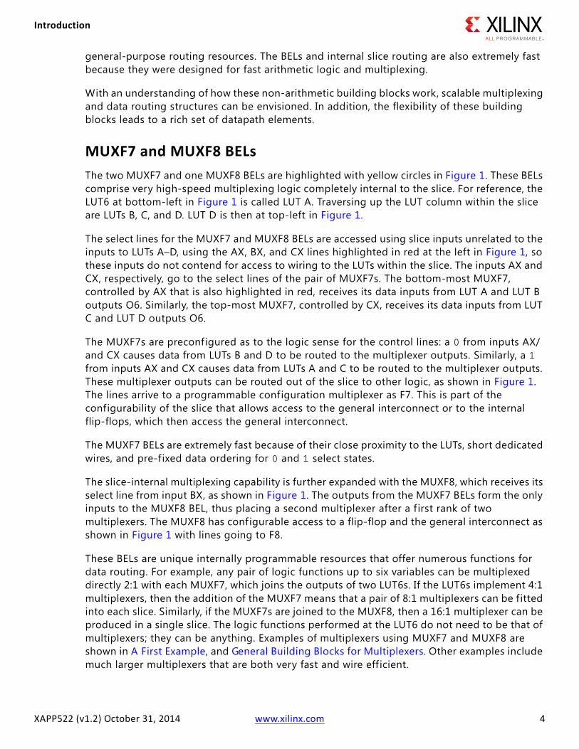
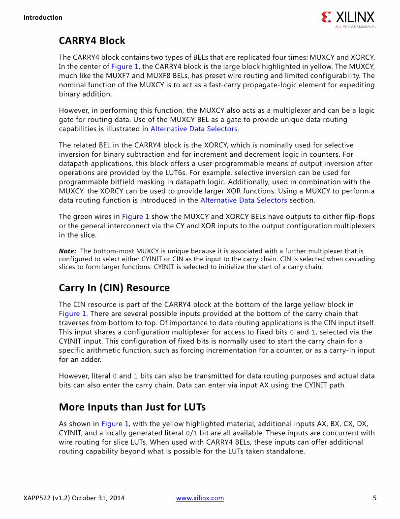
An 8-Bit Multiplexer Constructed within the FPGA SLICELAn 8-bit multiplexer only requires two cell designs comprised of a LUT6 and the internal MUXF7 BEL. Figure 2 shows the logic for a 4-bit cell called MUX4_CELL, plus the .INIT parameter necessary for programming the LUT6. The logic for the complete multiplexer is shown in Figure 3 where the two MUX4_CELLs are combined together with the internal MUXF7 multiplexer. In the structural HDL code for the composite multiplexer, there are only three instances (see Reference Design). All logic is compacted within half a slice, leaving the other half free. The wiring flow is inputs-then-outputs to a slice. No additional interconnect wires are required for the logic.
Table 1 shows the truth table for the MUX4_CELL shown in Figure 2. Table 2 shows the truth table of the complete 8-bit multiplexer of Figure 3.
The composite multiplexer can be treated as a cell design to aggregate multiplexers together for larger bitwidths. Same as the case for a lone 8-bit multiplexer cell, no additional interconnect wires are required for any width whatsoever. Also, two 8-bit multiplexers could be compacted into a single slice.
For the logic diagrams in this application note, the programmable LUT codes are shown in red. Techniques for understanding and creating user-custom LUT codes are explained in more detail in Appendix A: How to Create LUT Codes.
See FPGA Implementation for 8-Bit Multiplexer: Analysis and Figure 4 for information on implementing and how the MUX4_CELL and MUXF7 BEL work within the FPGA.
X-Ref Target - Figure 3
Figure 3: Slice-based 8:1 Multiplexer, Using 2x MUX4_CELL (LUT6) and 1x MUXF7
Table 1: Truth Table for MUX4_CELL: A 4-Bit Multiplexer Implemented in a LUT6
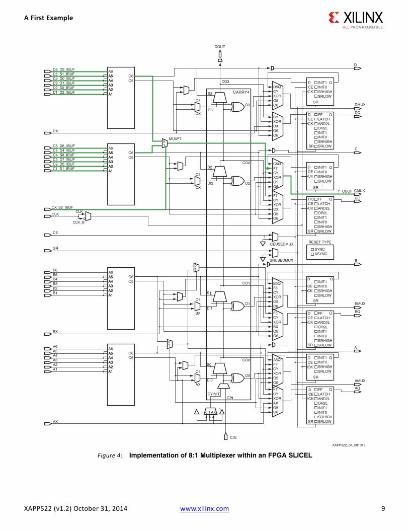
FPGA Implementation for 8-Bit Multiplexer: AnalysisFigure 4 shows how the 8-bit multiplexer can be placed in an FPGA SLICEL after using ISE tools for logic synthesis and then the implementation tools. The paths taken from input to output are highlighted in green. A similar result could also be obtained if the ISE tools used a SLICEM that was not needed in user logic as a memory.
The topology of Figure 4 is essentially identical to the logic drawing of Figure 3. Only half of the slice is used, that is, the upper C/D LUT6 and the upper MUXF7. The same logic could be implemented in the lower half instead. See General Building Blocks for Multiplexers for information on variations for other bit sizes.
1 0 X 1 X X 1
1 1 1 X X X 1
Table 2: Truth Table for a Complete 8-Bit Multiplexer
S2 S1 S0 I7 I6 I5 I4 I3 I2 I1 I0 O
0 0 0 X X X X X X X 0 0
0 0 1 X X X X X X 0 X 0
0 1 0 X X X X X 0 X X 0
0 1 1 X X X X 0 X X X 0
1 0 0 X X X 0 X X X X 0
1 0 1 X X 0 X X X X X 0
1 1 0 X 0 X X X X X X 0
1 1 1 0 X X X X X X X 0
0 0 0 X X X X X X X 1 1
0 0 1 X X X X X X 1 X 1
0 1 0 X X X X X 1 X X 1
0 1 1 X X X X 1 X X X 1
1 0 0 X X X 1 X X X X 1
1 0 1 X X 1 X X X X X 1
1 1 0 X 1 X X X X X X 1
1 1 1 1 X X X X X X X 1
Table 1: Truth Table for MUX4_CELL: A 4-Bit Multiplexer Implemented in a LUT6 (Cont’d)
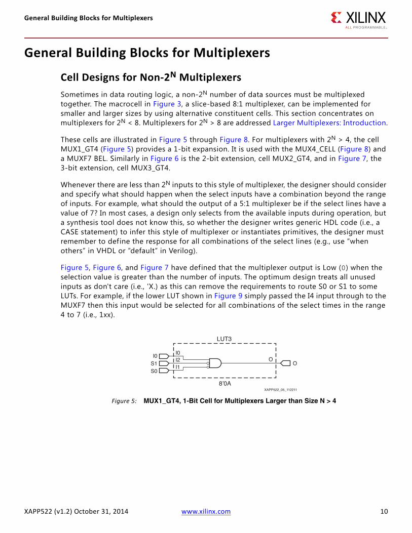
Cell Designs for Non-2N MultiplexersSometimes in data routing logic, a non-2N number of data sources must be multiplexed together. The macrocell in Figure 3, a slice-based 8:1 multiplexer, can be implemented for smaller and larger sizes by using alternative constituent cells. This section concentrates on multiplexers for 2N < 8. Multiplexers for 2N > 8 are addressed Larger Multiplexers: Introduction.
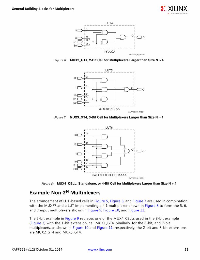
These cells are illustrated in Figure 5 through Figure 8. For multiplexers with 2N > 4, the cell MUX1_GT4 (Figure 5) provides a 1-bit expansion. It is used with the MUX4_CELL (Figure 8) and a MUXF7 BEL. Similarly in Figure 6 is the 2-bit extension, cell MUX2_GT4, and in Figure 7, the 3-bit extension, cell MUX3_GT4.
Whenever there are less than 2N inputs to this style of multiplexer, the designer should consider and specify what should happen when the select inputs have a combination beyond the range of inputs. For example, what should the output of a 5:1 multiplexer be if the select lines have a value of 7? In most cases, a design only selects from the available inputs during operation, but a synthesis tool does not know this, so whether the designer writes generic HDL code (i.e., a CASE statement) to infer this style of multiplexer or instantiates primitives, the designer must remember to define the response for all combinations of the select lines (e.g., use “when others” in VHDL or “default” in Verilog).
Figure 5, Figure 6, and Figure 7 have defined that the multiplexer output is Low (0) when the selection value is greater than the number of inputs. The optimum design treats all unused inputs as don't care (i.e., 'X.) as this can remove the requirements to route S0 or S1 to some LUTs. For example, if the lower LUT shown in Figure 9 simply passed the I4 input through to the MUXF7 then this input would be selected for all combinations of the select times in the range 4 to 7 (i.e., 1xx).
X-Ref Target - Figure 5
Figure 5: MUX1_GT4, 1-Bit Cell for Multiplexers Larger than Size N > 4
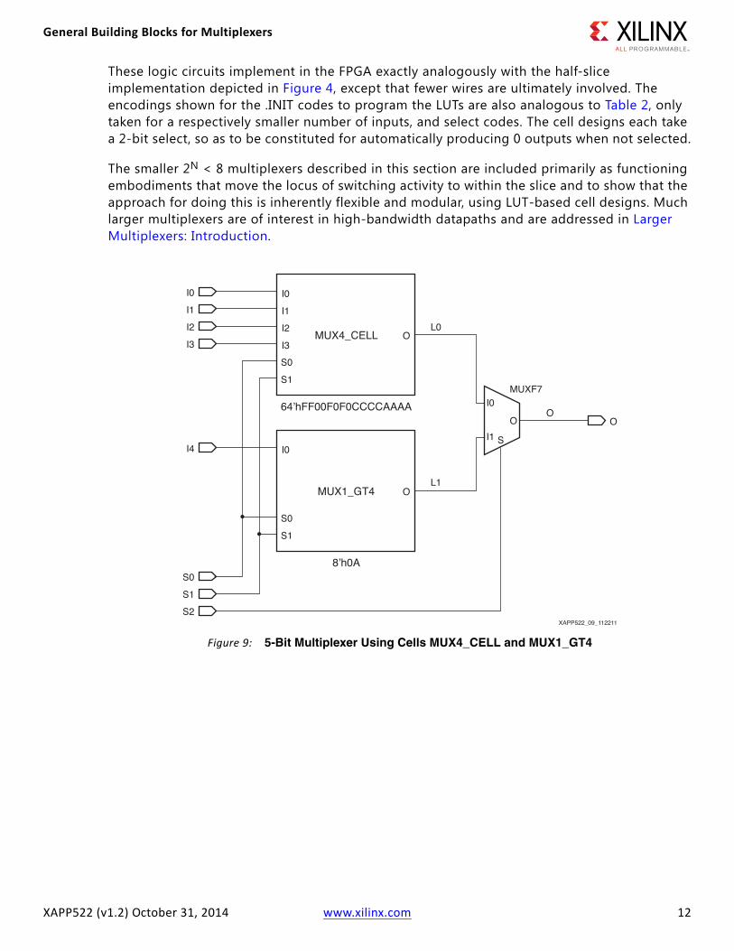
Example Non-2N MultiplexersThe arrangement of LUT-based cells in Figure 5, Figure 6, and Figure 7 are used in combination with the MUXF7 and a LUT implementing a 4:1 multiplexer shown in Figure 8 to form the 5, 6, and 7 input multiplexers shown in Figure 9, Figure 10, and Figure 11.
The 5-bit example in Figure 9 replaces one of the MUX4_CELLs used in the 8-bit example (Figure 3) with the 1-bit extension, cell MUX1_GT4. Similarly, for the 6-bit, and 7-bit multiplexers, as shown in Figure 10 and Figure 11, respectively, the 2-bit and 3-bit extensions are MUX2_GT4 and MUX3_GT4.
X-Ref Target - Figure 6
Figure 6: MUX2_GT4, 2-Bit Cell for Multiplexers Larger than Size N > 4
X-Ref Target - Figure 7
Figure 7: MUX3_GT4, 3-Bit Cell for Multiplexers Larger than Size N > 4
X-Ref Target - Figure 8
Figure 8: MUX4_CELL, Standalone, or 4-Bit Cell for Multiplexers Larger than Size N > 4
These logic circuits implement in the FPGA exactly analogously with the half-slice implementation depicted in Figure 4, except that fewer wires are ultimately involved. The encodings shown for the .INIT codes to program the LUTs are also analogous to Table 2, only taken for a respectively smaller number of inputs, and select codes. The cell designs each take a 2-bit select, so as to be constituted for automatically producing 0 outputs when not selected.
The smaller 2N < 8 multiplexers described in this section are included primarily as functioning embodiments that move the locus of switching activity to within the slice and to show that the approach for doing this is inherently flexible and modular, using LUT-based cell designs. Much larger multiplexers are of interest in high-bandwidth datapaths and are addressed in Larger Multiplexers: Introduction.
X-Ref Target - Figure 9
Figure 9: 5-Bit Multiplexer Using Cells MUX4_CELL and MUX1_GT4
Larger Multiplexers: IntroductionLarger multiplexers are comprised of additional cells. Using the MUXF8 BEL, a pair of the 8-bit multiplexers depicted in Figure 3 can be joined together to form a 16-bit multiplexer that f its within a single slice. This 16-bit multiplexer is shown in Figure 12. Per Figure 1, page 3, the MUXF8 data inputs connect directly to the pair of MUXF7 within the slice, forming an extremely fast internal 4:1 multiplexer adjoining all four LUT6 together. This capability is illustrated for reducing external wire count outside the slice; A 16:1 compression of inputs-to-outputs is possible with the 16-bit multiplexer. All inputs arrive to the slice, and the output exits from it, without any requirement for additional general purpose interconnect.
Like the 2N < 8 multiplexers, other variations for 2N < 16 are possible with the 16-bit multiplexer. For instance, a 14-bit multiplexer example is shown in Figure 13, substituting a MUX2_GT4 cell for the MUX4_CELL in the uppermost bit positions of the 16-bit multiplexer (Figure 12). However, it is important to remember that only the output of a MUXF7 can connect to the input of a MUXF8 and that the inputs to a MUXF7 must come from the outputs of the adjacent LUTs. This results in this style of multiplexer consuming a complete slice, even if it only has 9 inputs. Therefore, a designer that can structure a design that can maximize the use of inputs to the 8:1 and 16:1 multiplexers is rewarded by the naturally good fit of these elements within each slice. When the design allows, generic HDL can successfully decompose larger multiplexers by inserting pipeline registers at points consistent with flip-flops connected to the outputs of a MUXF7 or MUXF8.
16-Bit Multiplexer FPGA Implementation describes the internal connection of FPGA BELs that provide the multiplexer of Figure 12. The use of CASE statements in VHDL and Verilog generally result in the synthesis of the same circuits shown in Figure 12 and Figure 13 providing all selection states are defined (i.e., “when others” or “default” used when required). Instantiation of primitives guarantees the implemented circuit and might be the best way to control the implementation when decomposing larger multiplexer structures.
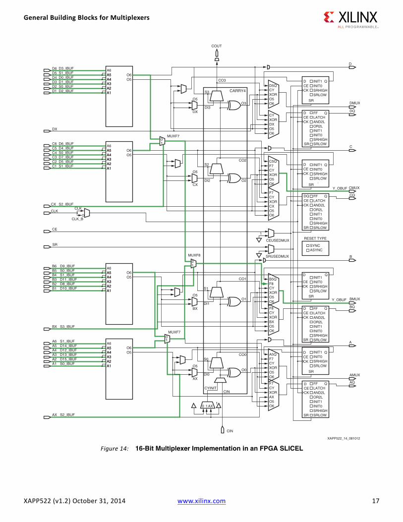
16-Bit Multiplexer FPGA ImplementationLike the organization of logic shown in Figure 12, the 16-bit multiplexer has an FPGA implementation that is topologically similar, as seen in Figure 14. That is, there is a 1:1 correspondence between the BELs called out in the logic drawing and its implementation in the FPGA. The color lines show the wiring path from all four LUT6 to the MUXF7s, then to the MUXF8, and f inally the output.
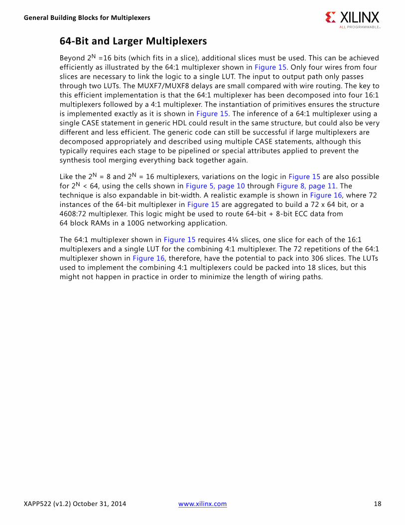
64-Bit and Larger MultiplexersBeyond 2N =16 bits (which f its in a slice), additional slices must be used. This can be achieved eff iciently as illustrated by the 64:1 multiplexer shown in Figure 15. Only four wires from four slices are necessary to link the logic to a single LUT. The input to output path only passes through two LUTs. The MUXF7/MUXF8 delays are small compared with wire routing. The key to this eff icient implementation is that the 64:1 multiplexer has been decomposed into four 16:1 multiplexers followed by a 4:1 multiplexer. The instantiation of primitives ensures the structure is implemented exactly as it is shown in Figure 15. The inference of a 64:1 multiplexer using a single CASE statement in generic HDL could result in the same structure, but could also be very different and less eff icient. The generic code can still be successful if large multiplexers are decomposed appropriately and described using multiple CASE statements, although this typically requires each stage to be pipelined or special attributes applied to prevent the synthesis tool merging everything back together again.
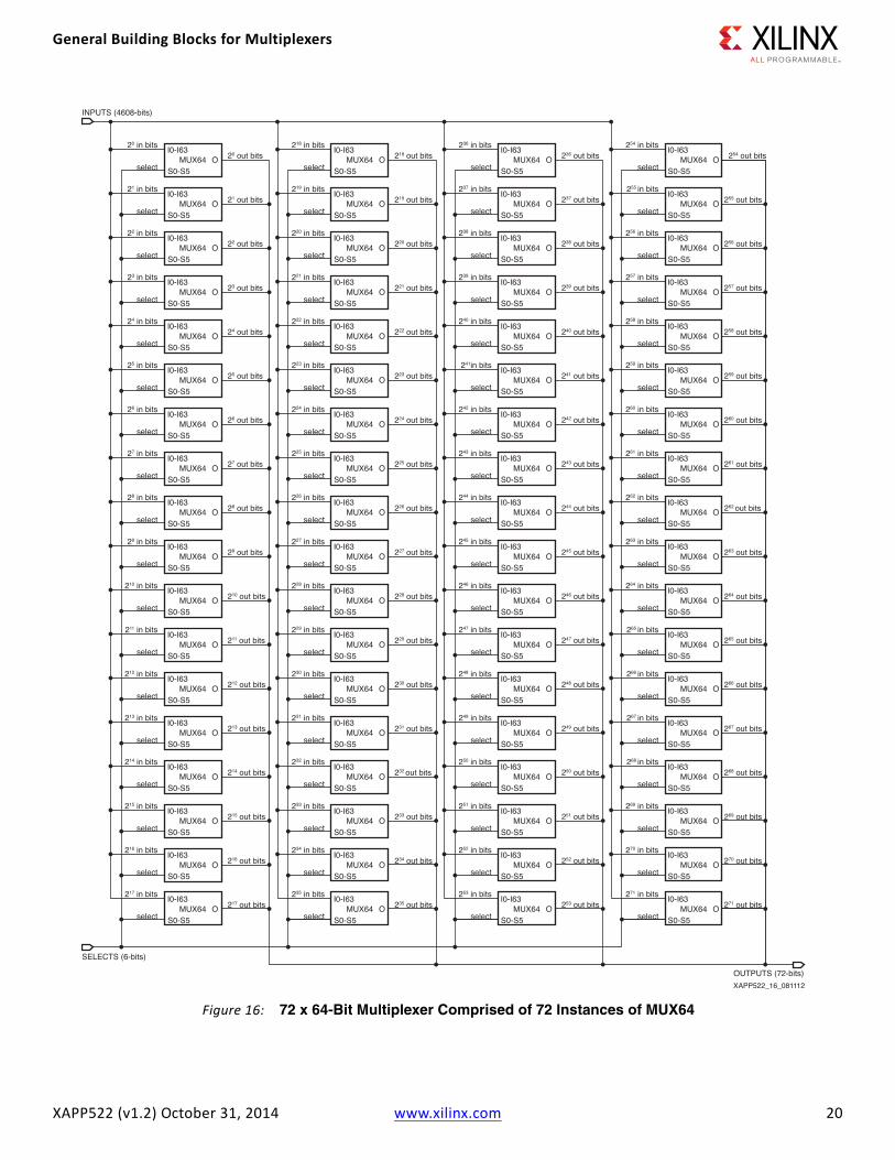
Like the 2N = 8 and 2N = 16 multiplexers, variations on the logic in Figure 15 are also possible for 2N < 64, using the cells shown in Figure 5, page 10 through Figure 8, page 11. The technique is also expandable in bit-width. A realistic example is shown in Figure 16, where 72 instances of the 64-bit multiplexer in Figure 15 are aggregated to build a 72 x 64 bit, or a 4608:72 multiplexer. This logic might be used to route 64-bit + 8-bit ECC data from 64 block RAMs in a 100G networking application.
The 64:1 multiplexer shown in Figure 15 requires 4¼ slices, one slice for each of the 16:1 multiplexers and a single LUT for the combining 4:1 multiplexer. The 72 repetitions of the 64:1 multiplexer shown in Figure 16, therefore, have the potential to pack into 306 slices. The LUTs used to implement the combining 4:1 multiplexers could be packed into 18 slices, but this might not happen in practice in order to minimize the length of wiring paths.
An Alternative to 2N Multiplexing: 1-of-N Data SelectorIn some system applications, the control logic that produces data select signals does not naturally offer binary encoding and sometimes extra logic is required to effect binary encoding, which would unnecessarily slow down the datapath. Examples include multiple parallel data lanes, such as BRAM memories, where data seen on one of the lanes has a special encoding to indicate how the aggregate of data on all lanes should be ordered. The pattern detection logic for the encoding pattern is similar to priority encoding, naturally producing 1-of-N signals, where a single control line among N lines selects which data to route. The select controls can also be described as being one-hot encoded meaning that only one select line is active (High) at any given time. However, in the case of a priority encoder more than one select line can be active at the same time with the select line allocated the highest priority exerting control over the data selected.
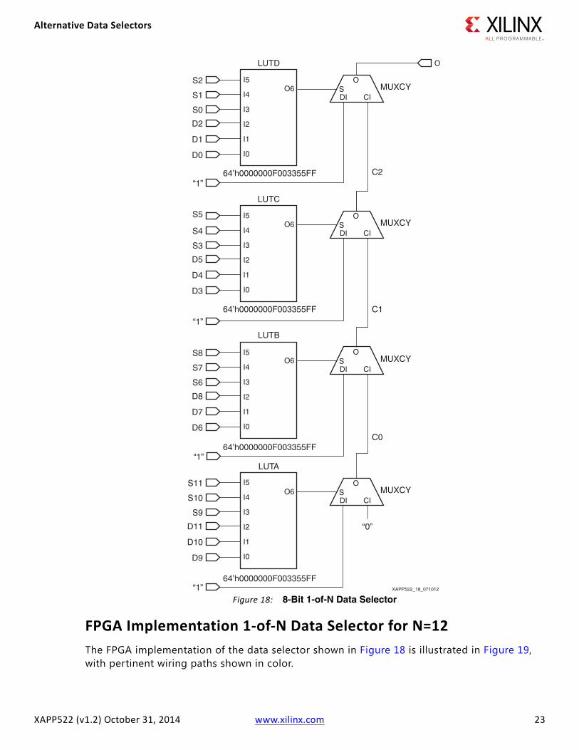
Figure 18 shows the efficient implementation of a 1-of-12 data selector which is the largest size that can be implemented within a single slice. Each LUT is programmed to implement a 1-of-3 data selector with an inverted output. In this case, the select controls are considered to be one-hot, but the LUT could be programmed to provide priority or any behavior required when more than one select input is active (High) at the same time. When any one of the select controls is High, the output of the LUT is the inverted logic level of the corresponding data input. However, when all three select controls are Low then the output of the LUT is forced High. While this would appear to be unexpected behavior for a 1-of-3 data selector, it is critical to the combining stage formed by the MUXCY elements and the dedicated carry chain within the CARRY4 block.
The output from each LUT controls the select input to its corresponding MUXCY. The DI inputs are driven permanently High (1) and the CI at the bottom (or start) of the chain is driven permanently Low (0). This arrangement configures the carry chain as a NAND gate with four inputs. If any of the S inputs are Low, a 1 is selected and passed up the carry chain to the output at the top. If all S inputs are High, all MUXCYs select their CI inputs and the 0 entering the bottom of the chain propagates through to the output at the top.
Consider now the operation of the 1-of-12 data selector when only the select signal S4 is active (High). The output from LUTA is High so the bottom MUXCY is selecting and propagating a 0 up the chain. Because S4 is active, the output from LUTB is the inverse of the level being presented to the D4 data input. So when D4 is Low, the output from LUTB is High and its associated MUXCY selects the CI input such that it continues to propagate the 0 up the carry chain. Alternatively, when D4 is High, the output from LUTB is Low and forces the MUXCY to select the DI input and propagate a 1 up the carry chain. Therefore, the logic level that passes up the carry chain reflects the logic level applied to the D4 input. With the outputs of both LUTC and LUTD being High, this level propagates though to the output at the top of the chain.
Extending the Data SelectorThe data selector described in this section can be made in a scalable manner by cascading slices vertically. There are zero interstitial wires between input and output. The limit for any usable scale is the size of any vertical column in the target FPGA. Because the carry chain between slices is extremely fast, very little added delay is incurred for larger scale data selectors (see Figure 17).
Tradeoffs between 1-of-N and 2N MultiplexingOne tradeoff for the 1-of-N data selectors versus 2N multiplexers is signaling speed versus density. For example, any multiplexer 2N > 16 is slower than a data selector because more one LUT traversal is required with additional interstitial wires. The data selector at any size only requires passing through one LUT, with zero interstitial wires. The price paid is density. The 1-of-N solution only compacts to 12 bits per slice, whereas 2N multiplexers can pack up to 16 bits per slice.
Almost certainly, the only way to implement the 1-of-N style correctly requires instantiation of primitives. Also the very nature of the 1-of-N technique can take some time to digest and apply in a design, but it really is worthy of serious consideration because it is often the better choice. The 1-of-N style has particular merit when it is also configured to provide priority encoding. Each LUT can be programmed to provide the function required and then the carry chain gives a natural priority to the top of the chain nearest the f inal output.
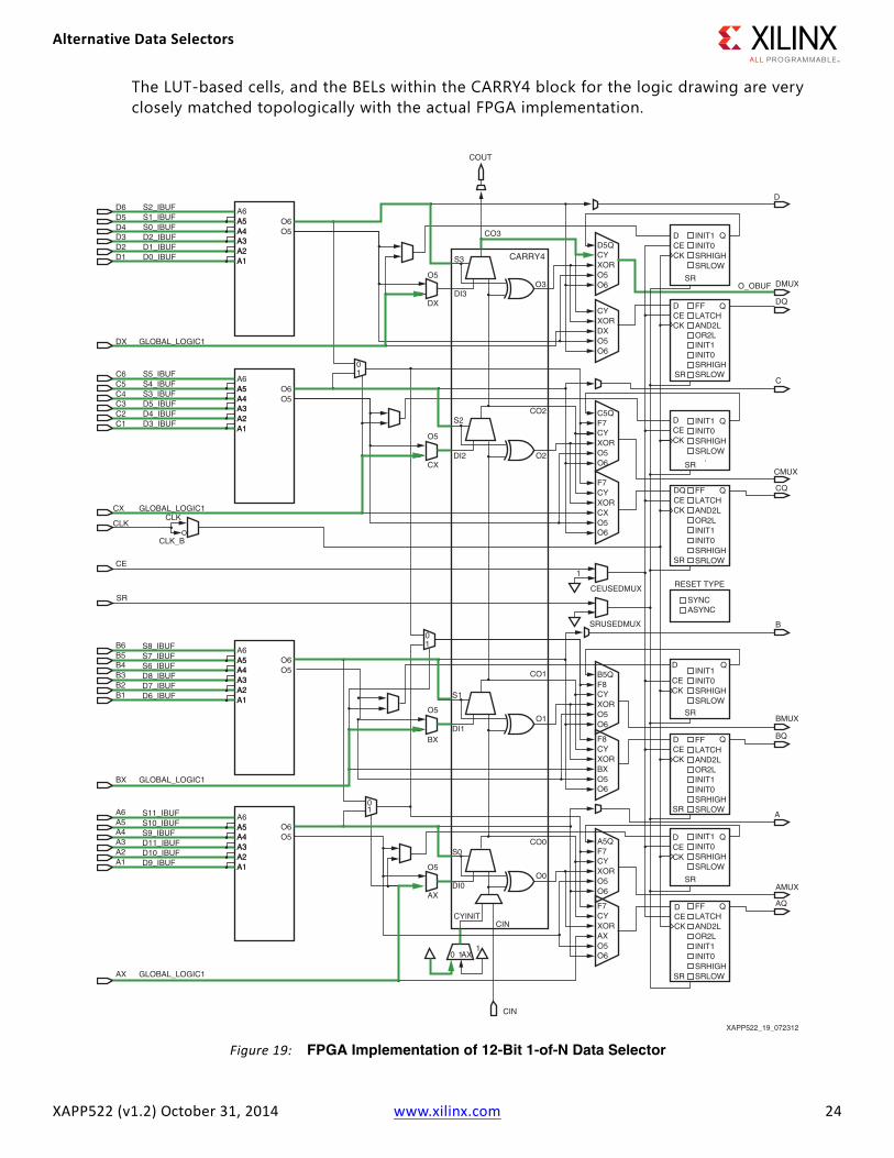
FPGA Implementation 1-of-N Data Selector for N=12The FPGA implementation of the data selector shown in Figure 18 is illustrated in Figure 19, with pertinent wiring paths shown in color.
The LUT-based cells, and the BELs within the CARRY4 block for the logic drawing are very closely matched topologically with the actual FPGA implementation.
X-Ref Target - Figure 19
Figure 19: FPGA Implementation of 12-Bit 1-of-N Data Selector
What: Locus of Switching Activity and Maximizing Fan-In CompressionAs seen in Figure 1, page 3, each slice can have up to 29 simultaneous inputs (24 for four LUT6, then AX, BX, CX, DX, CIN, and a local 0/1), not 24. The use of the carry chain within just the CARRY4 block multiplies the effect of the simultaneous inputs because additional logic switching operations can happen immediately after the LUT6 resources and at high speed.
The concept is “doing more logic” in a single rank, or using more of the slice, more often. Doing more logic switching in a single rank reduces the total number of LUTs, reduces LUT delays, and compresses the logic fan-in.
When more of the switching activity to decide the result of a datapath logic function is contained within a single slice, more external routing resources are conserved. As a result, a greater proportion of the general interconnect becomes available for data or control. Interconnect within the slice and across its localized carry chain within the CARRY4 is extremely fast. These infra-slice resources do not interfere with general purpose interconnect.
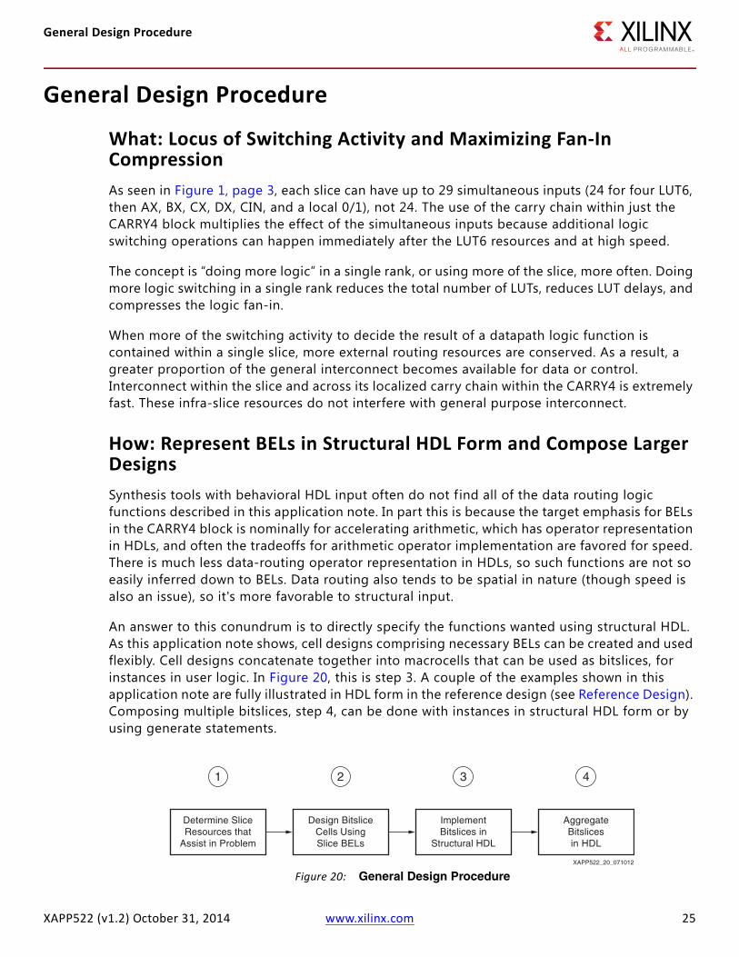
How: Represent BELs in Structural HDL Form and Compose Larger DesignsSynthesis tools with behavioral HDL input often do not f ind all of the data routing logic functions described in this application note. In part this is because the target emphasis for BELs in the CARRY4 block is nominally for accelerating arithmetic, which has operator representation in HDLs, and often the tradeoffs for arithmetic operator implementation are favored for speed. There is much less data-routing operator representation in HDLs, so such functions are not so easily inferred down to BELs. Data routing also tends to be spatial in nature (though speed is also an issue), so it's more favorable to structural input.
An answer to this conundrum is to directly specify the functions wanted using structural HDL. As this application note shows, cell designs comprising necessary BELs can be created and used flexibly. Cell designs concatenate together into macrocells that can be used as bitslices, for instances in user logic. In Figure 20, this is step 3. A couple of the examples shown in this application note are fully illustrated in HDL form in the reference design (see Reference Design). Composing multiple bitslices, step 4, can be done with instances in structural HDL form or by using generate statements.
Reference DesignYou can download the Reference Design Files for this application note from the Xilinx website.
Table 3 shows the reference design matrix.
Appendix A: How to Create LUT Codes
Implementation with LUTsFigure 1, page 3 illustrates LUTs in the block diagram of the FPGA SLICEL. The related SLICEM allows use of LUTs as memory elements, but this slice is actually conceptually no different than the SLICEL for the purposes of programming the LUTs for logic functions. Because the slice LUTs form a nexus of programmable logic functionality in the FPGA device, they drive much of what
is possible to do in creating system designs. The LUTs can be configured with hexadecimal initialization codes in HDL as shown in the reference design (see Reference Design). These codes program the LUT to exhibit a certain logic output, for a given set of inputs. With behavioral HDL synthesis, the configurations are obtainable automatically without entering codes directly—synthesis does this. But to have very specif ic functions for datapath-related functions, the user can create LUT codes directly.
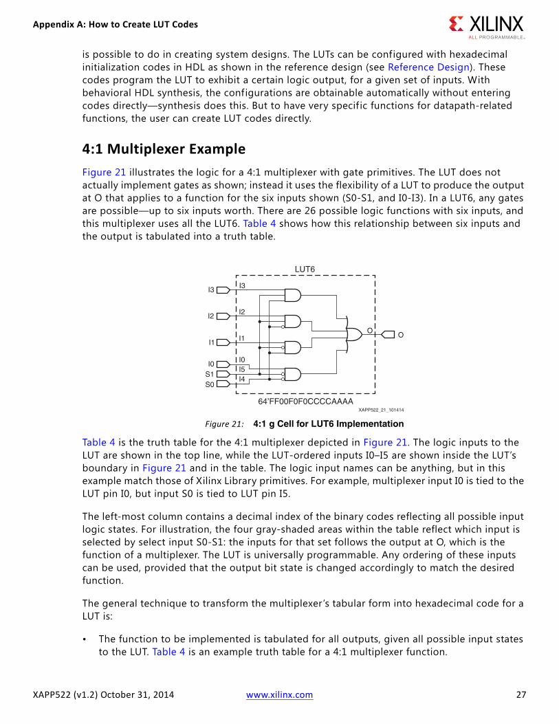
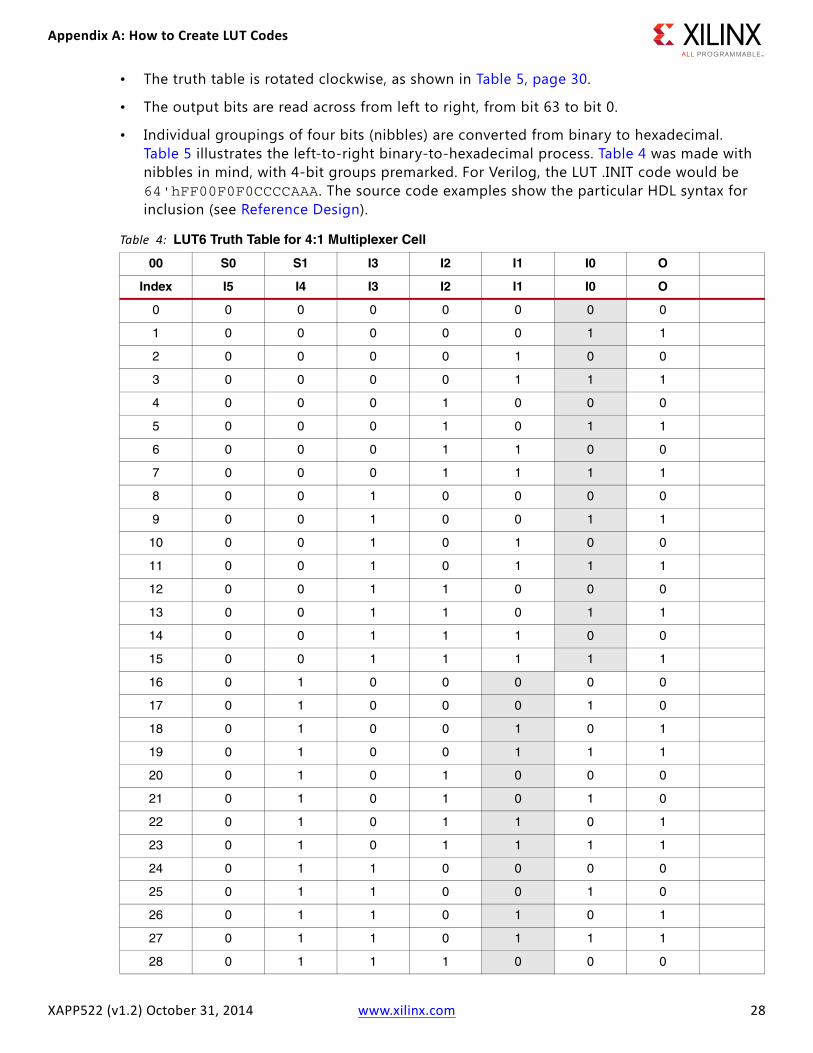
4:1 Multiplexer ExampleFigure 21 illustrates the logic for a 4:1 multiplexer with gate primitives. The LUT does not actually implement gates as shown; instead it uses the flexibility of a LUT to produce the output at O that applies to a function for the six inputs shown (S0-S1, and I0-I3). In a LUT6, any gates are possible—up to six inputs worth. There are 26 possible logic functions with six inputs, and this multiplexer uses all the LUT6. Table 4 shows how this relationship between six inputs and the output is tabulated into a truth table.
Table 4 is the truth table for the 4:1 multiplexer depicted in Figure 21. The logic inputs to the LUT are shown in the top line, while the LUT-ordered inputs I0–I5 are shown inside the LUT’s boundary in Figure 21 and in the table. The logic input names can be anything, but in this example match those of Xilinx Library primitives. For example, multiplexer input I0 is tied to the LUT pin I0, but input S0 is tied to LUT pin I5.
The left-most column contains a decimal index of the binary codes reflecting all possible input logic states. For illustration, the four gray-shaded areas within the table reflect which input is selected by select input S0-S1: the inputs for that set follows the output at O, which is the function of a multiplexer. The LUT is universally programmable. Any ordering of these inputs can be used, provided that the output bit state is changed accordingly to match the desired function.
The general technique to transform the multiplexer’s tabular form into hexadecimal code for a LUT is:
• The function to be implemented is tabulated for all outputs, given all possible input states to the LUT. Table 4 is an example truth table for a 4:1 multiplexer function.
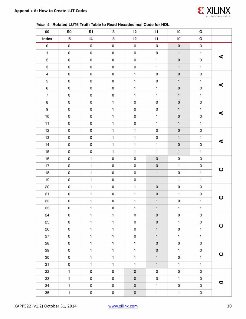
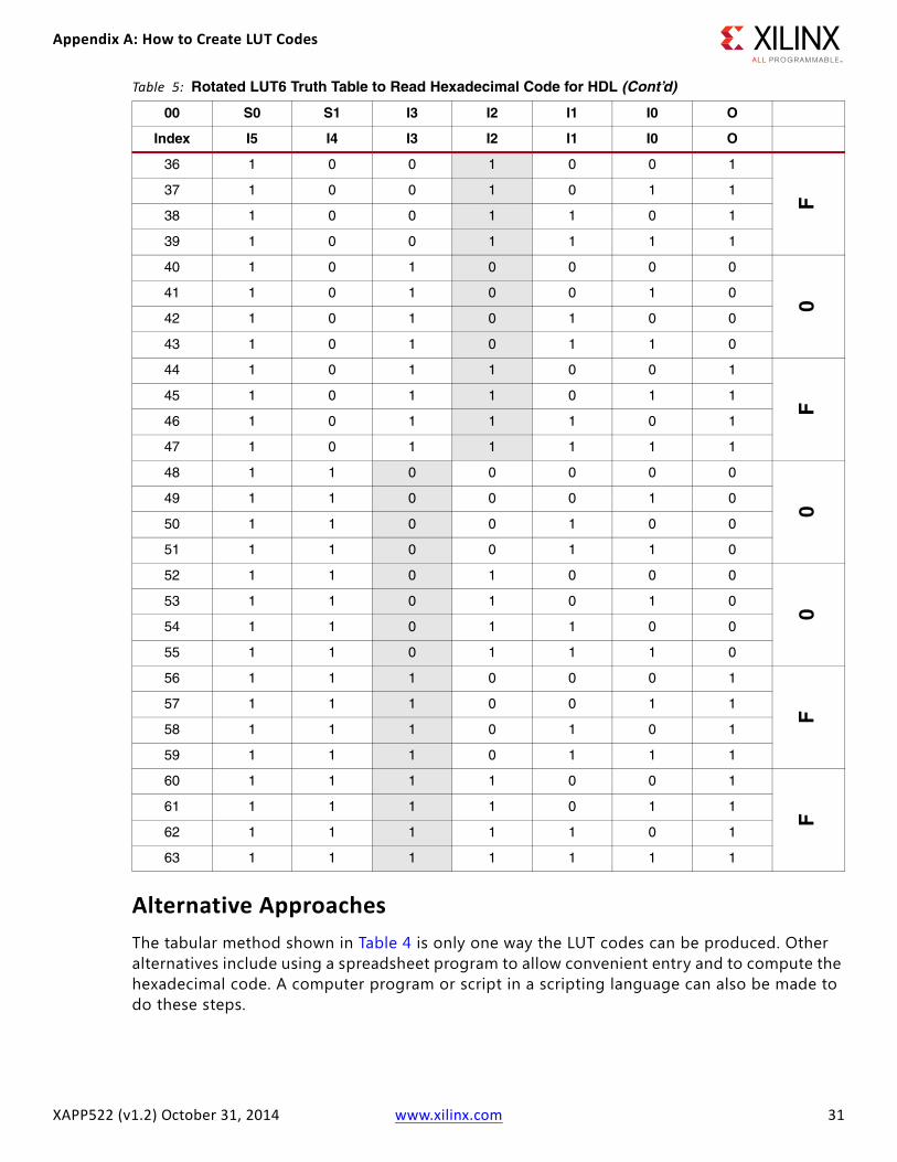
• The truth table is rotated clockwise, as shown in Table 5, page 30.
• The output bits are read across from left to right, from bit 63 to bit 0.
• Individual groupings of four bits (nibbles) are converted from binary to hexadecimal. Table 5 illustrates the left-to-right binary-to-hexadecimal process. Table 4 was made with nibbles in mind, with 4-bit groups premarked. For Verilog, the LUT .INIT code would be 64'hFF00F0F0CCCCAAA. The source code examples show the particular HDL syntax for inclusion (see Reference Design).
Table 4: LUT6 Truth Table for 4:1 Multiplexer Cell
Alternative ApproachesThe tabular method shown in Table 4 is only one way the LUT codes can be produced. Other alternatives include using a spreadsheet program to allow convenient entry and to compute the hexadecimal code. A computer program or script in a scripting language can also be made to do these steps.
36 1 0 0 1 0 0 1
F
37 1 0 0 1 0 1 1
38 1 0 0 1 1 0 1
39 1 0 0 1 1 1 1
40 1 0 1 0 0 0 0
0
41 1 0 1 0 0 1 0
42 1 0 1 0 1 0 0
43 1 0 1 0 1 1 0
44 1 0 1 1 0 0 1
F
45 1 0 1 1 0 1 1
46 1 0 1 1 1 0 1
47 1 0 1 1 1 1 1
48 1 1 0 0 0 0 0
0
49 1 1 0 0 0 1 0
50 1 1 0 0 1 0 0
51 1 1 0 0 1 1 0
52 1 1 0 1 0 0 0
0
53 1 1 0 1 0 1 0
54 1 1 0 1 1 0 0
55 1 1 0 1 1 1 0
56 1 1 1 0 0 0 1
F
57 1 1 1 0 0 1 1
58 1 1 1 0 1 0 1
59 1 1 1 0 1 1 1
60 1 1 1 1 0 0 1
F61 1 1 1 1 0 1 1
62 1 1 1 1 1 0 1
63 1 1 1 1 1 1 1
Table 5: Rotated LUT6 Truth Table to Read Hexadecimal Code for HDL (Cont’d)
ConclusionThe primary teaching of this application note is that focusing more switching activity within the slice through the direct use of the slice BELs reduces the general-purpose routing resources, offers high speed, and increases quality of results determinism. Direct access to the slice is possible by specifying BELs in structural HDL. For datapath-oriented system designs containing large numbers of bits, these techniques can be superior to that obtained with logic specif ied solely in behavioral HDL form.
Revision HistoryThe following table shows the revision history for this document.
08/30/2012 1.1 Modified text in FPGA Slice Building Blocks: Looking Within. Modif ied the heading An 8-Bit Multiplexer Constructed within the FPGA SLICEL. Modified title and added labels to Figure 1, Figure 4, and Figure 14. Colorized the MUX signal between MUXF7 and MUXF8 to green in Figure 14. Corrected labels in Figure 15 and Figure 16.
10/31/2014 1.2 Transposed pin labels I4 and I5 in Figure 2 and Figure 21.