LEE ET AL. VOL. 7 ’ NO. 1 ’ 301 –307 ’ 2013 www.acsnano.org 301 December 12, 2012 C 2012 American Chemical Society Engineering Electronic Properties of Graphene by Coupling with Si-Rich, Two-Dimensional Islands Dong Hyun Lee, † Jaeseok Yi, † Jung Min Lee, † Sang Jun Lee, § Yong-Joo Doh, § Hu Young Jeong, ^ Zonghoon Lee, ^, * Ungyu Paik, †,‡, * John A. Rogers, z and Won Il Park †, * † Department of Materials Science and Engineering and ‡ Department of Energy Engineering, Hanyang University, Seoul 133-791, Korea, § Department of Display and Semiconductor Physics, Korea University Sejong Campus, Sejong, 339-700, Korea, ^ Department of Mechanical & Advanced Materials Engineering, Ulsan National Institute of Science and Technology, Ulsan 689-798, Korea, and z Department of Materials Science and Engineering, University of Illinois at UrbanaChampaign, Urbana, Illinois 61801, United States T he potential of atomically thin graphene layers with excellent electrical 1,2 and thermal conduction and mechanical strength 4 has motivated research toward fu- ture electronics. 5 As graphene is a one-atom thick planar sheet of carbon atoms in a hon- eycomb crystal lattice, three electrons from each carbon atom involve strong sp 2 hybrid bonds with their neighbors that form a σ state, while the fourth electron is delocalized and develops into a π state. The extremely high mobility of graphene, with reported values in excess of 15 000 cm 2 V 1 s 1 at room tem- perature, is associated with its linear electronic band dispersion relation near the Dirac points such that the carriers (electrons and holes as- sociated with the π bands) behave like mass- less Dirac fermions. 6,7 On the other hand, the π bonding and π* antibonding states of graphene are degenerate at the Dirac points, and, thus, graphene exhibits a semimetallic behavior or zero-bandgap nature that limits the practical application in electronic devices. Several routes have been designed and implemented to engineer the bandgap in graphene without degrading its intrinsic carrier mobilities. 811 One route is the use of narrow graphene nanoribbons, 8,9 nano- meshes, 10 or quantum dots, 11 where lateral constriction of the charge carriers causes a bandgap. However, this approach requires patterning of graphene with a width much smaller than ∼10 nm to achieve a substan- tial bandgap, and the electronic structure is quite sensitive to the edge atomic config- uration and size. Hybridized structures con- sisting of a graphene matrix with a dispersed phase of wider gap 2D layer-structured mate- rials, such as hexagonal boron nitride (h-BN) sheets 12 or hydrogenated graphene 13 (i.e., graphane), were also introduced to induce electron confinement. However, electron scattering at the domain boundaries signif- icantly degraded the electronic properties. As the degeneration of the π and π* bands at the Dirac points is associated with the * Address correspondence to [email protected], [email protected], [email protected]. Received for review August 31, 2012 and accepted December 5, 2012. Published online 10.1021/nn304007x ABSTRACT Recent theoretical and experimental studies demonstrated that breaking of the sublattice symmetry in graphene produces an energy gap at the former Dirac point. We describe the synthesis of graphene sheets decorated with ultrathin, Si-rich two-dimensional (2D) islands (i.e., Gr:Si sheets), in which the electronic property of graphene is modulated by coupling with the Si-islands. Analyses based on transmission electron microscopy, atomic force microscopy, and electron and optical spectroscopies confirmed that Si-islands with thicknesses of ∼2 to 4 nm and a lateral size of several tens of nm were bonded to graphene via van der Waals interactions. Field-effect transistors (FETs) based on Gr:Si sheets exhibited enhanced transconductance and maximum-to-minimum current level compared to bare-graphene FETs, and their magnitudes gradually increased with increasing coverage of Si layers on the graphene. The temperature dependent currentvoltage measurements of the Gr:Si sheet showed approximately a 2-fold increase in the resistance by decreasing the temperature from 250 to 10 K, which confirmed the opening of the substantial bandgap (∼2.53.2 meV) in graphene by coupling with Si islands. KEYWORDS: graphene . silicon islands . van der Waals growth . bandgap engineering . sublattice asymmetry ARTICLE
Transcript
LEE ET AL. VOL. 7 ’ NO. 1 ’ 301–307 ’ 2013
www.acsnano.org
301
December 12, 2012
C 2012 American Chemical Society
Engineering Electronic Properties ofGraphene by Coupling with Si-Rich,Two-Dimensional IslandsDong Hyun Lee,† Jaeseok Yi,† Jung Min Lee,† Sang Jun Lee,§ Yong-Joo Doh,§ Hu Young Jeong,^
Zonghoon Lee,^,* Ungyu Paik,†,‡,* John A. Rogers,z and Won Il Park†,*
†Department of Materials Science and Engineering and ‡Department of Energy Engineering, Hanyang University, Seoul 133-791, Korea, §Department of Display andSemiconductor Physics, Korea University Sejong Campus, Sejong, 339-700, Korea, ^Department of Mechanical & Advanced Materials Engineering, Ulsan NationalInstitute of Science and Technology, Ulsan 689-798, Korea, and zDepartment of Materials Science and Engineering, University of Illinois at Urbana�Champaign,Urbana, Illinois 61801, United States
The potential of atomically thingraphenelayers with excellent electrical1,2 andthermal conduction and mechanical
strength4 has motivated research toward fu-ture electronics.5 As graphene is a one-atomthick planar sheet of carbon atoms in a hon-eycomb crystal lattice, three electrons fromeach carbon atom involve strong sp2 hybridbondswith their neighbors that formaσ state,while the fourth electron is delocalized anddevelops into a π state. The extremely highmobility of graphene, with reported values inexcess of 15000 cm2 V�1 s�1 at room tem-perature, is associatedwith its linear electronicband dispersion relation near the Dirac pointssuch that the carriers (electrons and holes as-sociated with the π bands) behave like mass-less Dirac fermions.6,7 On the other hand, theπ bonding and π* antibonding states ofgraphene are degenerate at the Dirac points,and, thus, graphene exhibits a semimetallicbehavior or zero-bandgap nature that limitsthe practical application in electronic devices.
Several routes have been designed andimplemented to engineer the bandgap ingraphene without degrading its intrinsiccarrier mobilities.8�11 One route is the useof narrow graphene nanoribbons,8,9 nano-meshes,10 or quantum dots,11 where lateralconstriction of the charge carriers causes abandgap. However, this approach requirespatterning of graphene with a width muchsmaller than ∼10 nm to achieve a substan-tial bandgap, and the electronic structure isquite sensitive to the edge atomic config-uration and size. Hybridized structures con-sisting of a graphene matrix with a dispersedphase of wider gap 2D layer-structured mate-rials, such as hexagonal boron nitride (h-BN)sheets12 or hydrogenated graphene13 (i.e.,graphane), were also introduced to induceelectron confinement. However, electronscattering at the domain boundaries signif-icantly degraded the electronic properties.As the degeneration of the π and π* bandsat the Dirac points is associated with the
Received for review August 31, 2012and accepted December 5, 2012.
Published online10.1021/nn304007x
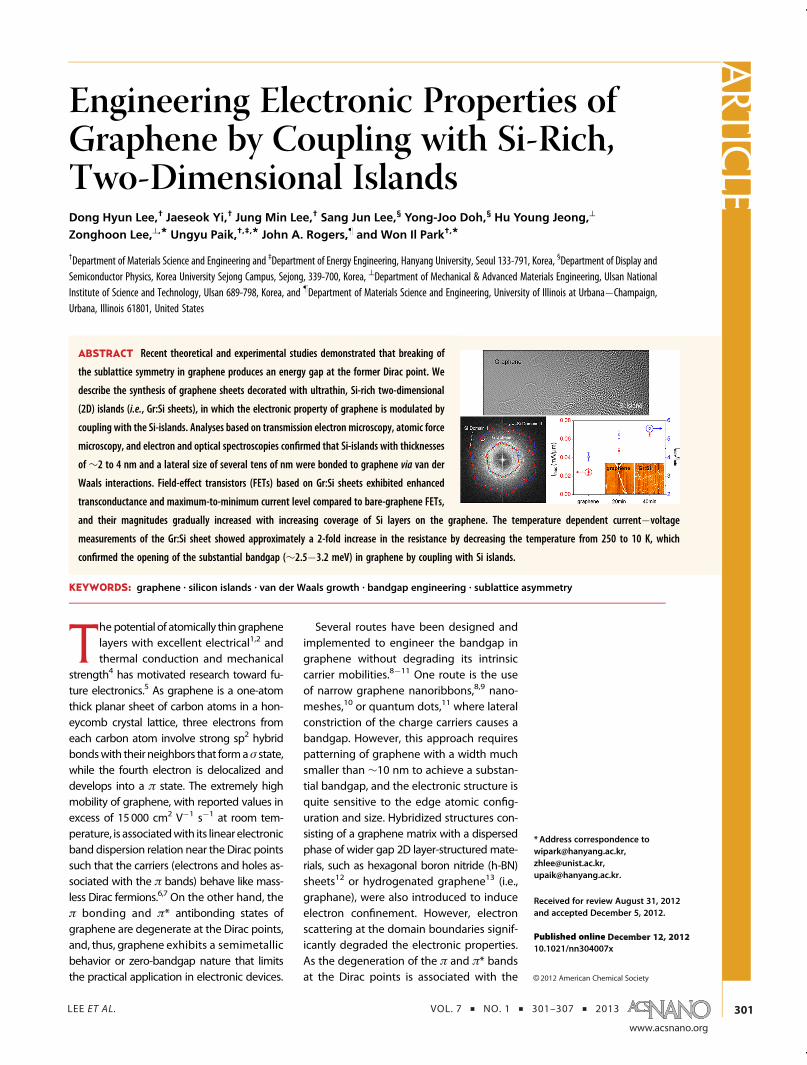
ABSTRACT Recent theoretical and experimental studies demonstrated that breaking of
the sublattice symmetry in graphene produces an energy gap at the former Dirac point. We
describe the synthesis of graphene sheets decorated with ultrathin, Si-rich two-dimensional
(2D) islands (i.e., Gr:Si sheets), in which the electronic property of graphene is modulated by
coupling with the Si-islands. Analyses based on transmission electron microscopy, atomic force
microscopy, and electron and optical spectroscopies confirmed that Si-islands with thicknesses
of∼2 to 4 nm and a lateral size of several tens of nm were bonded to graphene via van der
Waals interactions. Field-effect transistors (FETs) based on Gr:Si sheets exhibited enhanced
transconductance and maximum-to-minimum current level compared to bare-graphene FETs,
and their magnitudes gradually increased with increasing coverage of Si layers on the graphene. The temperature dependent current�voltage
measurements of the Gr:Si sheet showed approximately a 2-fold increase in the resistance by decreasing the temperature from 250 to 10 K, which
confirmed the opening of the substantial bandgap (∼2.5�3.2 meV) in graphene by coupling with Si islands.
KEYWORDS: graphene . silicon islands . van der Waals growth . bandgap engineering . sublattice asymmetry
ARTIC
LE
LEE ET AL. VOL. 7 ’ NO. 1 ’ 301–307 ’ 2013
www.acsnano.org
302
lattice symmetry of carbon atoms in a honeycombcrystal lattice,14 the breaking of the sublattice symme-try is an alternative to open its bandgap.15 One exam-ple is the substrate-induced bandgap opening ofgraphene epitaxially grown on specific substrates,16
such as silicon carbide (SiC); however, their existenceand origin are still under debate. Moreover, the use ofspecific substrates imposes severe restrictions on theapplication of graphene.In this study, the engineering bandgap in graphene
was investigated by introducing Si-rich, two-dimensional(2D) islands dispersed on the graphene sheet. In thegraphene sheet decorated with Si-islands (Gr:Si sheet),the interaction between graphene and the islands breaksthe sublattice symmetry and thereby opens the bandgap.
RESULTS AND DISCUSSION
Synthesis and Transfer of Gr:Si Sheets. As a first step ofthis study, single-layer graphene sheetswere grown oncopper foils by the custom-built CVD at 1000 �C for30 min. After transferring the graphene to Si/SiO2 sub-strate, a vapor transport route using Si lumps as sourcematerials was used to deposit Si-islands on graphene.The deposition process was performed in a flow-ing H2/Ar atmosphere at 1000 �C for 20�60 min (seeMethods section and Supporting Information Figure S1).Because of the strong sp2-hybridized C�C bond ingraphene, displacement of C by Si hardly occurred.Instead, physisorbed Si adatoms formed very thin Si-islands bonded to the graphene via van der Waals in-teractions. Even after the Si island deposition, graphene
sheets sustained their 2D layered form such that theywere readily separated from the growth substrates andtransferred to other substrates for characterization anddevice fabrication (see the Methods section and Sup-porting Information, Figure S1). A continuous form of alarge area (∼1� 2 cm2) Gr:Si sheet transferred to a glasssubstrate is shown in the inset of Figure 1a. Additionaloptical transmittancemeasurements reveal that the sam-ple was highly transparent with an average transmissionof∼97% in the visible spectral range (Figure 1a), which iscomparable to monolayer graphene.17,18
Figure 1b shows the low-magnification transmis-sionelectronmicroscopy (TEM) imageof a free-standingmembrane with a lateral size of several micrometers.The central region of the sample reveals the character-istic feature of atomically thin 2D layered structures,whereas the edges of the free-standing sheets tendedto fold back enabling the layer number to bemeasured.TEM examination confirmed the formation of a mono-layer or∼2�3 layer sheets (inset, Figure 1b). In addition,atomic force microscopy (AFM) surface topography ofthe Gr:Si sheet reveals a continuous sheet with the ex-ception of a few wrinkles, which is similar to that of theCVD-grown graphene sheet (Figure 1c,d). Meanwhile,white bumps were distributed relatively uniformly ongraphene (Figure 1d,e). These bumps correspond to Siislands, and their height and width were estimated as∼1�3 nm and ∼20�50 nm, respectively (Figure 1f).
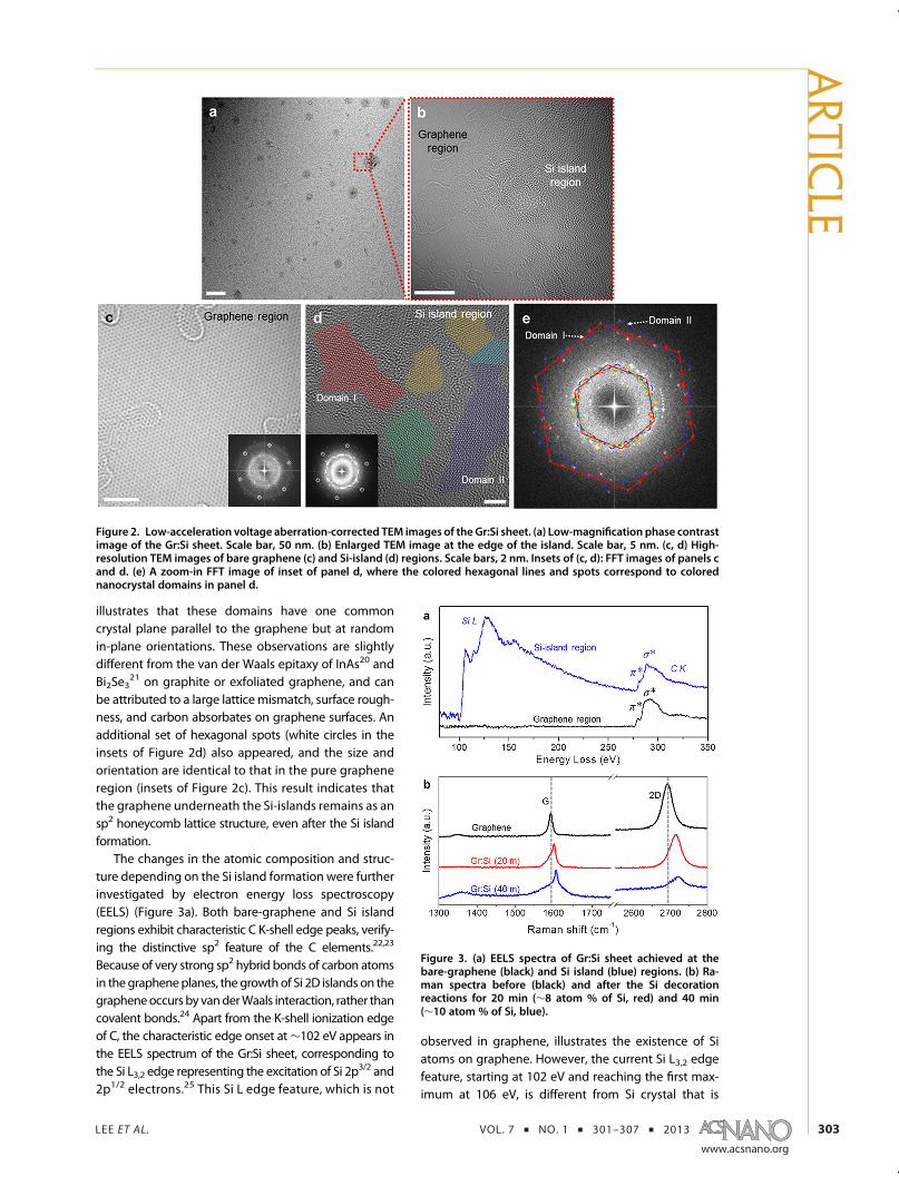
Structural and Composition Analyses. Further struc-tural characterization was performed using a low-acceleration voltage aberration-corrected TEM analysis.As shown in the low-magnification phase contrast image(Figure 2a), uniform distribution of the islands on thegraphene sheet was visualized by dark contrast fea-tures, which is analogous to the AFM results. Themagnified TEM image at the edge of the islands revealthat the atomic structures of the islands are distinctlydifferent from that of graphene (Figure 2b). A lattice-resolved image obtained by zooming in on one of thegraphene regions illustrates that significant areas ofthe graphene regions appear clean with near-perfectatomic arrangements in a honeycomb crystal lattice,except for the carbon adsorbates near the edge of theimage (Figure 2c). In Si-rich island regions, polycrystal-line structures, consisting of nanocrystalline domains,are clearly visible (Figure 2d). Each domain exhibitshexagonal lattice fringes with an adjacent lattice spa-cing of 0.19 nm, which is consistent with the d-spacingof the Si (022) planes.19 The corresponding fast Fouriertransformation (FFT) image transformed from Figure 2ereveals the existence of several sets of hexagonaldiffraction patterns with identical size and configura-tion. Additionally, each set is identical to the Si [111]zone axis patterns, confirming that the preferred crys-tal orientation perpendicular to the graphene surface is[111]. Several color-shade domains in Figure 2d corre-spond to the diffraction patterns in Figure 2e, which
Figure 1. (a) Optical transmittance spectrum of the Gr:Sisheet. Inset: photograph of the Gr:Si sheet transferred to aglass substrate. Scale bar, 1 cm. (b) Low-magnification TEMimage of the free-standing Gr:Si fragment deposited on aholey carbon grid. Scale bar, 200 nm. Inset: TEM image ofthe edge of themonolayer Gr:Si sheet. Scale bar, 5 nm. (c, d)Comparison of AFM surface topographies of graphene (c)and Gr:Si (d) sheets. Scale bars, 1 μm. (e) Enlarged AFMimage of a selective area in panel d. Scale bar, 100 nm.(f) Height profile along the black dotted line.
ARTIC
LE
LEE ET AL. VOL. 7 ’ NO. 1 ’ 301–307 ’ 2013
www.acsnano.org
303
illustrates that these domains have one commoncrystal plane parallel to the graphene but at randomin-plane orientations. These observations are slightlydifferent from the van der Waals epitaxy of InAs20 andBi2Se3
21 on graphite or exfoliated graphene, and canbe attributed to a large latticemismatch, surface rough-ness, and carbon absorbates on graphene surfaces. Anadditional set of hexagonal spots (white circles in theinsets of Figure 2d) also appeared, and the size andorientation are identical to that in the pure grapheneregion (insets of Figure 2c). This result indicates thatthe graphene underneath the Si-islands remains as ansp2 honeycomb lattice structure, even after the Si islandformation.
The changes in the atomic composition and struc-ture depending on the Si island formation were furtherinvestigated by electron energy loss spectroscopy(EELS) (Figure 3a). Both bare-graphene and Si islandregions exhibit characteristic C K-shell edge peaks, verify-ing the distinctive sp2 feature of the C elements.22,23
Because of very strong sp2 hybrid bonds of carbon atomsin thegrapheneplanes, the growthof Si 2D islands on thegrapheneoccursby vanderWaals interaction, rather thancovalent bonds.24 Apart from the K-shell ionization edgeof C, the characteristic edge onset at∼102 eV appears inthe EELS spectrum of the Gr:Si sheet, corresponding tothe Si L3,2 edge representing the excitation of Si 2p
3/2 and2p1/2 electrons.25 This Si L edge feature, which is not
observed in graphene, illustrates the existence of Siatoms on graphene. However, the current Si L3,2 edgefeature, starting at 102 eV and reaching the first max-imum at 106 eV, is different from Si crystal that is
Figure 2. Low-acceleration voltage aberration-corrected TEM images of the Gr:Si sheet. (a) Low-magnification phase contrastimage of the Gr:Si sheet. Scale bar, 50 nm. (b) Enlarged TEM image at the edge of the island. Scale bar, 5 nm. (c, d) High-resolution TEM images of bare graphene (c) and Si-island (d) regions. Scale bars, 2 nm. Insets of (c, d): FFT images of panels cand d. (e) A zoom-in FFT image of inset of panel d, where the colored hexagonal lines and spots correspond to colorednanocrystal domains in panel d.
Figure 3. (a) EELS spectra of Gr:Si sheet achieved at thebare-graphene (black) and Si island (blue) regions. (b) Ra-man spectra before (black) and after the Si decorationreactions for 20 min (∼8 atom % of Si, red) and 40 min(∼10 atom % of Si, blue).
ARTIC
LE
LEE ET AL. VOL. 7 ’ NO. 1 ’ 301–307 ’ 2013
www.acsnano.org
304
characterized by amain peak starting near 100 eV witha first maximum at∼101�102 eV. The shift of the edgespectrummay be associated with the oxidation and/orcarbidation states of Si.26 As the crystalline Si structurewas confirmed in the TEM image and absence of O Kedge peak in EELS spectrum (see Supporting Informa-tion, Figure S2), the Si islands consisted of extremelythin Si domains whose surface and boundary can beoxidized/carbidized easily, resulting in the change inthe absorption spectrum.
Figure 3b displays the evolution of the Raman spectrafollowing the reaction of Siwith graphene sheets. Uniquefeatures include the increase in the disorder-induced Dbands (∼1350�1355 cm�1), broad background signaland a decrease in 2D bands, which illustrates the gradualchange from the original graphene characteristics. Inaddition, both the G and 2D bands of the Gr:Si sheetsshift toward higher frequencies in the graphene spec-trum, from 1592 to 1601 cm�1 and 2692 to 2,713 cm�1,respectively.27 The shift in the G band (9 cm�1) is muchgreater than that of the 2D band (21 cm�1) and differentmechanisms can be introduced to explain these shifts.The signal shift in the G band accompanying Si decora-tion is explained by local electron/hole doping in carbon-based materials.28 Even though local doping can affectthe 2D band of the carbon material, a 2D band shift of21 cm�1 is too large to occur with such doping.29 Instead,
the strain effect can explain the 2D band shift of Gr:Sistructures, as similar phenomena have been observedin epitaxial graphene grown on a SiC substrate29 and aBe2Se3 nanoplate
21 on graphene.Electrical Properties of the Gr:Si Sheets. To investigate
the electrical properties of the Gr:Si sheets, back-gatefield-effect transistors (FETs) were fabricated on a de-generately doped nþ-Si wafer with a 300-nm thickoxide layer, following the procedure described in theSupporting Information. Specifically, the capability oflarge-area transfer and patterning of arbitrary shapeswith nanometer or micrometer features enables thecreation of large-scale FET arrays (Figure 4a). Opticaland SEM images illustrate that the FETs consisted of Gr:Si channels with a width of 5 μm and source-drainelectrode pair with a gap of 10 μm. Figure 4b comparesthe source-drain current (Id) versus back-gate voltage(Vg) characteristic curves for graphene andGr:Si sheets,which illustrates several interesting points. First, com-pared with the graphene-FET exhibiting a minimalconductance at a finite gate voltage (correspondingto the Dirac point) at ∼20 V, Gr:Si FETs exhibit shifts intheir Dirac points up to 40�60 V, indicating that theyoperate more as p-channel transistors. Second, themaximum current (Imax) (or current at Vg of �80 V)increases from 0.125 mA to 0.229 mA for the Gr:Si FETwith the Si reactions for 20 min (∼8 atom % Si) and to
Figure 4. Field-effect transistor characteristics of Gr:Si sheets. (a) SEM images and schematic illustration of the Gr:Si FET array.Scale bars: 500 μm, 30 μm. (b) ID�VG characteristic curves at a VD of 1 V recorded for typical FETs with a graphene channel(black) and Gr:Si channels synthesized via Si reactions for 20 min (∼8 atom % Si, red) and 40 min (∼10 atom % Si, blue).(c) Statistical analyses of Imax/Imin and Imax as a function of the Si decoration reaction time. (d) Temperature-dependentelectrical transport measurement result of Gr:Si (∼8 atom % of Si) FET.
ARTIC
LE
LEE ET AL. VOL. 7 ’ NO. 1 ’ 301–307 ’ 2013
www.acsnano.org
305
0.342 mA for 40 min (∼10 atom % Si) with respect tothe graphene FET. Third, following the Imax increase,themaximum-to-minimum current ratio (Imax/Imin) alsogradually increased from 4.0 to 5.2 and 5.5 withincreasing Si-concentration. The enhanced Imax/Imin
ratio and the Dirac point shifts strongly suggest thegradual conversion of Gr:Si sheet characteristics fromsemimetallic to semiconducting. Moreover, statisticalanalyses of 30 devices reveal similar behaviors. Asshown in Figure 4c, the Imax increased by a factor of∼3 and the Imax/Imin increased from∼4 to 5.5, after theSi reaction for 40 min. From the slope of the Id�Vgcurve, a peak transconductance, GM = dId/dVg, of Gr:SiFETs was ∼3 μS, corresponding to a calculated holemobility of μ=∼780 cm2/(V 3 s). This value is larger thanthat of pristine-graphene FET (∼360 cm2/(V 3 s)) andalso analogous to the previously reported values ofgraphene FET (∼1,000 cm2/(V 3 s)),
30 illustrating thatalloy disorder scattering is not severe in this sample.12
In addition, we have investigated change in the ID�VGcharacteristics before and after Si island formation,using a different batch of graphene sheets than thoseused for the data in Figure 4b,c, and their results aredisplayed in Supporting Information, Figure S3.Although the electrical properties of graphene FETsin Figure S3 are different from those in Figure 4b,c, theeffect of Si island deposition on the Imax and Imax/Imin
ratio are essentially same.Moreover, temperature-dependent electrical trans-
port measurements on Gr:Si sheets with the Si reac-tions for 20 min (∼8 atom % Si) show the resistanceincreases by decreasing temperature from 250 to 10 K(Figure 4d), which is different from that of grapheneand corresponds to a typical semiconducting behavior.The electrical resistance of the Gr:Si sheet as a functionof temperature is given as Arrhenius plots in the insetof Figure 4d. The linear relationship between thelogarithm of resistance and inverse of temperatureconfirmed that the Arrhenius law was satisfied, withwhich the bandgap energy was calculated as 2.5 meV.Moreover, the measured bandgap of Gr:Si sheetsincreased with increasing Si coverage, from 2.5 meVfor 8 atom % Si to 3.2 meV for 10 atom % Si(Supporting Information, Figure S4). We believe thatthe bandgap generation originated from the breakingof the A,B sublattice symmetry of graphene caused bycoupling with the ultrathin Si-islands. Similar phenom-ena have been observed in bi- or trilayer graphene31,32
and monolayer graphene grown epitaxially on the SiCsubstrate,16 where the interactions between differentlayers can cause the graphene to lose the 6-fold rota-tional symmetry near the Dirac point, breaking theA,B sublattice equivalence.11,16,32 However, the band-gap energy of 3.2 meV is too small in comparison withthose of epitaxial graphene grown on a SiC substrate(∼250 meV), and can be attributed to the small cover-age of Si islands (less than 10%). In this case, modulation
of the band structure occurs only in localized regionsof graphene just below the Si islands. We thereforeexpect that the substantial bandgap created by cou-pling with Si-islands should be much greater than themeasured values (of 3.2 meV), and thus the bandgapenergy of the Gr:Si can be further enlarged by increas-ing the Si coverage.
The bandgap creation is associated with the im-proved Imax/Imin ratio in the Gr:Si FETs; however, itsmagnitude is ten times smaller than the thermalenergy at room temperature (26 meV) such that theGr:Si FETs could not be fully turned off. However, theother changes observed in the Gr:Si FETs, that is, theenhanced current level, transconductance, and field-effect mobility, cannot be solely understood by themodulation of the bandgap. We believe that the Sidecoration process resulted in the recovery of defectsin graphene,33 such as Stone-Wales defects,34 vacan-cies of carbon atoms, and line defects at the grainboundary that deteriorate the charge carrier transportin graphene. Recent theoretical calculations based on adensity functional theory predicted the substitution-ally doped Si atoms in graphene do not significantlydisturb the quantum conductance of the pristinegraphene, which is distinctly different from other ele-ments (such as B, N, P, and S) that cause defect scat-tering in graphene.35 Accordingly, defect reconstruc-tion accompanying Si incorporation could be anotherpossible scenario, where Si atoms occupying the va-cancy sites in graphene can lead to an injection ofcharge carriers into the electrical system of graphenewithout providing any significant defect scatteringsites. On the other hand, Si-islands on graphene canbreak not only the A,B sublattice symmetry but alsothe electron�hole symmetry in pristine graphene. Theresulting electron�hole asymmetry caused the self-doping effect that is associated with the Dirac pointshift (downshift of the Fermi level) in the graphenenear the Si-islands,36 leading to a current level increasein the Gr:Si FETs. This self-doping effect created a syn-ergy with a bandgap opening to enhance the trans-conductance and motility of the Gr:Si FETs.
CONCLUSIONS
Large-area synthesis of graphene sheets decollatedwith Si-islands was performed. Analyses based on AFMand aberration-corrected TEM revealed that a few nmthick 2D Si-islands were tightly bonded to graphene byvan der Waals interactions. Even after Si island deposi-tion, the graphene layermaintained its sp2 honeycombstructures, as confirmed by EELS and Raman spectros-copy. Importantly, electrical transport measurementsshowed that the electronic properties of graphene canbe modulated by coupling with the Si-islands, leadingto a bandgap opening and an improvement of thetransistor characteristics, including the current level, trans-conductance, and mobility of the Gr:Si FETs compared to
ARTIC
LE
LEE ET AL. VOL. 7 ’ NO. 1 ’ 301–307 ’ 2013
www.acsnano.org
306
the pristine graphene-FETs. This new Gr:Si structure pro-vides an opportunity to control the electronic band
structure ingraphene-integrated systemsandan intriguingpossibility of flexible, wearable, and invisible electronics.
METHODSSynthesis of Gr:Si Nanosheets. Initially, a large, mostly single
layer graphene specimen was synthesized on copper foils bychemical vapor deposition (CVD) and then mounted onto a Sisubstrate with a 300-nm-thick SiO2 layer. A detailed descriptionof the CVD synthesis and transfer of graphene can be foundelsewhere.18,37 Immediately following the transfer, the graphenefilms on SiO2/Si substrateswere loaded into the CVD tube reactor(1 in. diameter quartz tube) again, where tiny fragments of singlecrystal Si in an alumina cruciblewere placed at a distance 3�4 cmupstream from the growth substrates. The decoration reactionof graphene into Gr:Si sheets was carried out at 1000 �C for20�60 min, while the pressure was maintained in the range of50�200 Torr under the continuous supply of a 30�50 SCCMH2/Ar gas mixture (10% H2 in Ar).
Transfer of the Gr:Si Sheets to Arbitrary Substrates. After synthesisof the Gr:Si sheet, it was separated from the SiO2/Si substrate byselective etching of the SiO2 layer. Typically, the filmwas initiallycoated with a poly(methyl methacrylate) (PMMA C9) protectinglayer, and then dipped in 1:10 HF-solution. After rinsing theseparated Gr:Si/PMMA film in deionized (DI) water, it was trans-ferred to a target substrate for analysis and characterization. ThePMMA protecting layer was typically removed with acetone.
TEM and EELS Measurements. The approach that utilizes directtransfer of the Gr:Si/PMMA film to the TEM grid and subsequentremoval of the PMMAwith acetone cannot fully remove residualPMMA on the surface, which significantly affects the high-resolution TEM analysis of the sheet. To minimize the amountof residual PMMA, we slightly modified the transfer method forTEM measurement. After preparing the Gr:Si/PMMA film byfollowing the procedure described in the previous section, itwas transferred to another copper foil. Subsequently, the PMMAsupport was completely removed with acetone. Finally, the Gr:Sisheet was detached from the copper foil with diluted ammoniumpersulfateacid and then transferred to theTEMgrid.Wenoted thatthe freestanding Gr:Si sheet with no supporting layer was easilycracked and torn, but its fragments several micrometers to milli-meters in lateral size could be easily found in the grid. High-resolution TEM, electron diffraction, and EELS analyseswere carriedout with an aberration-corrected TEM which operated at 80 keV.
Transistor Fabrication and Electrical Characterization. The Gr:Sisheet was transferred onto a heavily doped nþ-Si wafer with a300-nm-thick oxide layer to fabricate the back-gate field-effecttransistor. Channels of the Gr:Si transistor with a 5 μm widthwere patterned by conventional photolithography, followed byoxygen plasma etching at 50 W for 1 min. Subsequently, thesecond photolithography process and thermal evaporation ofTi/Au (10 nm/50 nm) were performed to define the source�drain electrodes. To reduce the contact resistance, the SiC-sheetfield-effect transistor was thermally annealed at 380 �C for 90 sin the vacuum. Electrical measurements were conducted usinga probe station with a semiconductor parameter analyzer(model HP4145A).
Conflict of Interest: The authors declare no competingfinancial interest.
Supporting Information Available: Additional figures as de-scribed in the text. This material is available free of charge viathe Internet at http://pubs.acs.org.
Acknowledgment. This work was supported by NationalResearch Foundation of Korea (NRF) through Grant No.K20704000003TA050000310, Global Research Laboratory (GRL)Program provided by the KoreanMinistry of Education, Science,and Technology (MEST) in 2011 and by Basic Science ResearchProgram through the National Research Foundation of Korea(NRF) funded by the Ministry of Education, Science and Tech-nology (MEST) (2012-001442, 2012-0002881).
REFERENCES AND NOTES1. Morozov, S. V.; Novoselov, K. S.; Katsnelson, M. I.; Schedin,
F.; Elias, D. C.; Jaszczak, J. A.; Geim, A. K. Giant IntrinsicCarrier Mobilities in Graphene and Its Bilayer. Phys. Rev.Lett. 2008, 100, 016602.
2. Chen, J.-H.; Jang, C.; Xiao, S.; Ishigami, M.; Fuhrer, M. S.Intrinsic and Extrinsic Performance Limits of GrapheneDevices on SiO2. Nat. Nanotechnol. 2008, 3, 206–209.
3. Balandin, A. A.; Ghosh, S.; Bao, W.; Calizo, I.; Teweldebrhan,D.; Miao, F.; Lau, C. N. Superior Thermal Conductivity ofSingle-Layer Graphene. Nano Lett. 2008, 8, 902–907.
4. Lee, C.; Wei, X.; Kysar, J. W.; Hone, J. Measurement of theElastic Properties and Intrinsic Strength of MonolayerGraphene. Science 2008, 321, 385–388.
5. Wang, Y.; Shao, Y.; Matson, D. W.; Li, J.; Lin, Y. Nitrogen-Doped Graphene and Its Application in ElectrochemicalBiosensing. ACS Nano 2010, 4, 1790–1798.
6. Zhang, Y. B.; Tan, Y. W.; Stormer, H. L.; Kim, P. ExperimentalObservation of the Quantum Hall Effect and Berry's Phasein Graphene. Nature 2005, 438, 201–204.
7. Novoselov, K. S.; Geim, A. K.; Morozov, S. V.; Jiang, D.;Katsnelson, M. I.; Grigorieva, I. V.; Dubonos, S. V.; Firsov,A. A. Two-Dimensional Gas of Massless Dirac Fermions inGraphene. Nature 2005, 438, 197–200.
8. Nakada, K.; Fujita, M.; Dresselhaus, G.; Dresselhaus, M. S.Edge State in Graphene Ribbons: Nanometer Size Effectand Edge Shape Dependence. Phys. Rev. B 1996, 54,17954–17961.
9. Brey, L.; Fertig, H. A. Electronic States of Graphene Nano-ribbons Studiedwith theDirac Equation. Phys. Rev. B 2006,73, 235411.
13. Elias, D. C.; Nair1, R. R.; Mohiuddin, T. M. G.; Morozov, S. V.;Blake, P. M.; Halsall, P.; Ferrari, A. C.; Boukhvalov, D. W.;Katsnelson, M. I.; Geim, A. K.; et al. Control of Graphene'sProperties by Reversible Hydrogenation: Evidence forGraphane. Science 2009, 323, 610–613.
14. Ohta, T.; Bostwick, A.; Seyller, T.; Horn, K.; Rotenberg, E.Controlling the Electronic Structure of Bilayer Graphene.Science 2006, 313, 951–954.
15. Partoens, B.; Peeters, F. M. From Graphene to Graphite:Electronic Structure around the K Point. Phy. Rev. B 2006,74, 075404.
16. Zhou, S. Y.; Gweon, G.-H.; Fedorov, A. V.; First, P. N.; DeHeer,W. A.; Lee, D.-H.; Guinea, F.; Castro, A. H.; Lanzara, A.Substrate-Induced Bandgap Opening in Epitaxial Gra-phene. Nat. Mater. 2007, 6, 770–775.
17. Bae, S. K.; Kim, H. K.; Lee, Y. B.; Xu, X. F.; Park, J. S.; Zheng, Y.;Balakrishnan, J. K.; Lei, T.; Kim, H. R.; Song, Y. I.; et al. Roll-to-Roll Production of 30-Inch Graphene Films for TransparentElectrodes. Nat. Nanotechnol. 2010, 5, 574–578.
18. Li, X.; Zhu, Y.; Cai, W.; Borysiak, M.; Han, B.; Chen, D.; Piner,R. D.; Colombo, L.; Ruoff, R. S. Transfer of Large-AreaGraphene Films for High-Performance Transparent Con-ductive Electrodes. Nano Lett. 2009, 9, 4359–4363.
19. Walther, T.; England, J. Investigation of Boron Implantationinto Silicon by Quantitative Energy-Filtered TransmissionElectron Microscopy. J. Phys.: Conf. Ser. 2011, 326, 012053.
20. Hong, Y. J.; Lee, W. H.; Wu, Y.; Ruoff, R. S.; Fukui, T. van derWaals Epitaxy of InAs Nanowires Vertically Aligned onSingle-Layer Graphene. Nano Lett. 2012, 12, 1431–1436.
ARTIC
LE
LEE ET AL. VOL. 7 ’ NO. 1 ’ 301–307 ’ 2013
www.acsnano.org
307
21. Dang, W.; Peng, H.; Li, H.; Wang, P.; Liu, Z. EpitaxialHeterostructures of Ultrathin Topological Insulator Nano-plate and Graphene. Nano Lett. 2010, 10, 2870–2876.
22. Berger, S. D.; McKenzie, D. R.; Martin, P. J. EELS Analysis ofVacuum Arc-Deposited Diamond-Like Films. Philos. Mag.Lett. 1988, 57, 285–290.
23. Chu, P. K.; Li, L. Characterization of Amorphous andNanocrystalline Carbon Films. Mater. Chem. Phys. 2006,96, 253–277.
24. Hong, Y. J.; Fukui, T. Controlled van der Waals Heteroepi-taxy of InAs Nanowires on Carbon Honeycomb Lattices.ACS Nano 2011, 5, 7576–7584.
25. Weng, X.; Rez, P.; Batson, P. E. Single Electron Calculationsfor the Si L2,3 Near Edge Structure. Solid State Commun.1990, 74, 1013–1015.
26. Pippel, E.; Lichtenberger, O.; Woltersdorf, J. Identificationof Silicon Oxycarbide Bonding in Si-C-O-Glasses by EELS.J. Mater. Sci. Lett. 2000, 19, 2059–2060.
27. Barros, E. B.; Demir, N. S.; Souza Filho, A. G.; Filho, J. M.; Jorio,A.; Dresselhaus, G.; Dresselhaus, M. S. Raman Spectroscopyof Graphitic Foams. Phys. Rev. B 2005, 71, 165422.
28. Pisana, S.; Lazzeri, M.; Casiraghi, C.; Novoselov, K. S.; Geim,A. K.; Ferrari, A. C.; Mauri, F. Breakdown of the AdiabaticBorn�Oppenheimer Approximation in Graphene. Nat.Mater. 2007, 6, 198–201.
29. Ni, Z. H.; Chen, W.; Fan, X. F.; Kuo, J. L.; Yu, T.; Wee, A. T. S.;Shen, Z. X. Raman Spectroscopy of Epitaxial Graphene on aSiC Substrate. Phys. Rev. B 2008, 77, 115416.
31. Mallet, P.; Varchon, F.; Naud, C.; Magaud, L.; Berger, C.;Veuillen, J.-Y. Electron States of Mono- and Bilayer Gra-phene on SiC Probed by STM. Phys. Rev. B 2007, 76,041403.
32. Rutter, G. M.; Crain, J. N.; Guisinger, N. P.; Li, T.; First, P. N.;Stroscio, J. A. Scattering and Interference in EpitaxialGraphene. Science 2007, 317, 219–222.
33. Guo, B.; Liu, Q.; Chen, E.; Zhu, H.; Fang, L.; Gong, J. R.Controllable N-Doping of Graphene. Nano Lett. 2010, 10,4975–4980.
34. Telling, R. H.; Heggie, M. I. Radiation Defects in Graphite.Philos. Mag. 2007, 87, 4797–4846.
35. Terrones, H.; Lv, R.; Terrones, M.; Dresselhaus, M. S. The Roleof Defects and Doping in 2D Graphene Sheets and 1DNanoribbons. Rep. Prog. Phys. 2012, 75, 062501.
36. Reich, S.; Maultzsch, J.; Thomsen, C.; Ordejón, P. Tight-Binding Description of Graphene. Phys. Rev. B 2002, 66,035412.
37. Li, X.; Cai, W.; An, J.; Kim, S.; Nah, J.; Yang, D.; Piner, R.;Velamakanni, A.; Jung, I.; Tutuc, E.; et al. Large-Area Synth-esis of High-Quality and Uniform Graphene Films onCopper Foils. Science 2009, 324, 1312–1314.


![Electronic and transport properties of kinked graphene · outstanding electronic transport properties of graphene [1]. However, it is crucial to modify the semimetallic electronic](https://static.documents.pub/doc/80x56/5fd887529019ff628275f4c6/electronic-and-transport-properties-of-kinked-graphene-outstanding-electronic-transport.jpg)


