Study on Electronic and Optical Properties of Graphene Oxide Under an External Electric Field From First-principles Abdehaヲd Najim Sultan Moulay Slimane University: Universite Sultan Moulay Slimane Omar BAJJOU ( [email protected]) Sultan Moulay Slimane University: Universite Sultan Moulay Slimane https://orcid.org/0000-0003- 0346-3847 Mustapha BOULGHALLAT Universite Sultan Moulay Slimane de Beni-Mellal Mohammed Khenfouch Ibn Zohr University: Universite Ibn Zohr Khalid Rahmani University Sultan Moulay Slimane of Beni-Mellal: Universite Sultan Moulay Slimane de Beni-Mellal Research Article Keywords: External electric ヲeld, Optical property, First-principle calculation, electronic structure, absorption spectrum Posted Date: November 3rd, 2021 DOI: https://doi.org/10.21203/rs.3.rs-996018/v1 License: This work is licensed under a Creative Commons Attribution 4.0 International License. Read Full License
Transcript
Study on Electronic and Optical Properties ofGraphene Oxide Under an External Electric FieldFrom First-principlesAbdeha�d Najim
Sultan Moulay Slimane University: Universite Sultan Moulay SlimaneOmar BAJJOU ( [email protected] )
Sultan Moulay Slimane University: Universite Sultan Moulay Slimane https://orcid.org/0000-0003-0346-3847Mustapha BOULGHALLAT
Universite Sultan Moulay Slimane de Beni-MellalMohammed Khenfouch
Ibn Zohr University: Universite Ibn ZohrKhalid Rahmani
University Sultan Moulay Slimane of Beni-Mellal: Universite Sultan Moulay Slimane de Beni-Mellal
STUDY on electronic and optical properties of graphene oxide under an external electric field from first-principles
Electronic and optical properties of graphene oxide (GO), under an external electric field (𝐸𝑒𝑥𝑡)
applied in three directions of space (x, y, z), are investigated using the density functional theory
(DFT). The application of the 𝐸𝑒𝑥𝑡, causes a significant modifications to the electronic and optical
properties of GO material. It has change the band gap, total density of states (TDOS), partial density
of states (PDOS), absorption coefficient (α), dielectric function, optical conductivity, refractive
index and loss function. The band gap of GO layer increases under the effects of the 𝐸𝑒𝑥𝑡, applied
in x and y directions. On the other hand, for z direction, the band gap decreases by the effects of the 𝐸𝑒𝑥𝑡. The peaks of the TDOS around the Fermi level, change by the 𝐸𝑒𝑥𝑡 applied in (x, y, z)
directions. The α peaks of the GO sheet, decreases by the 𝐸𝑒𝑥𝑡 applied in x direction, and increases
if 𝐸𝑒𝑥𝑡 applied in y and z directions. It is found that, the electronic and optical properties of GO
layer, could be affected by the effects of the 𝐸𝑒𝑥𝑡 and by its direction of application.
Keywords: External electric field, Optical property, First-principle calculation, electronic structure,
absorption spectrum.
1. Introduction
Electronic states of graphene derived from π electrons of the carbon atoms, can be calculated using the DFT
calculation. In two-dimensional graphene, the carbon atoms form a triangular lattice with the lattice
constant 𝑎 = √3 𝑑𝑐−𝑐 , and the carbon bond length in graphene sheet is dc-c= 0.142 nm [1]. A single layer
of graphene, the band structure shows zero gap at the K point of the Brillouin zone. This points is also
termed Dirac points, which can be opened by the external perturbations such as the application of the 𝐸𝑒𝑥𝑡
or by the strain [2]. Hofmann and Holst proposed a structural model of GO layer, with the epoxy groups
(C2O) only. They supposed that the oxygen functional groups, are bound to the carbon atoms of the hexagon
sheet planes [3]. Yan et al. [4,5] studied the arrangement of the epoxy groups on graphene layer, using the
first-principles calculations. The epoxy groups are orderly arranged in a chained on the basal plane of
graphene, forming specific oxygen-containing groups put on the both sides of graphene sheet.
In several cases, the effects of the 𝐸𝑒𝑥𝑡 can modify the electric current in a semiconductor device [6].
The electric field is simply modifiable in directions. The effects of the 𝐸𝑒𝑥𝑡 adjust the optical response of
the 2D graphene. The external dc gates control the Fermi energy and help the photocurrents in graphene
material, which are essential for optical modulators and photodetectors, respectively [7]. Therefore, it is
very necessary to study the effects of the 𝐸𝑒𝑥𝑡, on optical and electronic properties of GO. The effects of
the 𝐸𝑒𝑥𝑡 has the advantage of being easy to attain and control the physical properties of 2D materials. The 𝐸𝑒𝑥𝑡 applied on electronic and optical properties of GO, have received great attract for fundamental and
applied research.
Applying an electric field on materials can cause an electro-optical effects, and change their optical and
electronic properties [8,9]. In this paper, the effects of an 𝐸𝑒𝑥𝑡 on electronic structure and optical properties
of GO layer, are studied using the first-principles calculations [10]. Including the band gap, density of states
and optical properties of GO structure. In the case of applying the 𝐸𝑒𝑥𝑡 on GO layer, a perturbation of
electrostatic potential to the Hamiltonian of π-electrons is expected. The effects of an 𝐸𝑒𝑥𝑡 applied in the
three directions (x, y, z) of space, modifies the Hamiltonian H of the system as:
𝐻 = 𝐻0 − 𝑒𝐸𝑥 (1)
𝐻 = 𝐻0 − 𝑒𝐸𝑦 (2)
𝐻 = 𝐻0 − 𝑒𝐸𝑧 (3)
Where 𝐻0 is the Hamiltonian of the system without the effects of the 𝐸𝑒𝑥𝑡. Our paper is outlined as follows: In section 2, we briefly present the Computational Methods. Section 3
is devoted to discuss the numerical results and give our interpretations. Finally, the conclusions of our study
is included in Section 4.
2. Computational methods
The electronic structure simulations and optical properties of the GO model, are calculated based on the
DFT calculations. All calculations are performed using the CASTEP code, by the OTFG ultrasoft
pseudopotentials [11,12]. Only the valence electrons (C 2s22p2 and O 2s22p4) are considered using ultrasoft
pseudopotentials. The exchange-correlation energy was treated within the generalized gradient
approximation (GGA) in the form of Perdew, Burke and Ernzerhof (PBE) functional [13]. A plane‐wave
energy cut-off was set to 600 eV for all the calculations.
The K-point of the Brillouin zone was sampled using 6×6×1 gamma-centered Monkhorst-Pack grid
during the geometry optimizations of GO [14]. However, during all structural relaxations, the convergence
tolerance criteria for the geometry optimization was set to 2x10⁻⁶ eV/atom for the energy. During the atomic
relaxations, the positions of atoms are optimized until the convergence of the force on each atom, was less
than 0.003 eV/Å and 0.005 Å for the displacement. The self-consistent field (SCF) convergence tolerance,
was set to 2x10⁻⁶ eV/atom. The internal stress components are less than 0.1 GPa.
In the present simulation, the GO structure is shown in Fig.1. In this model, each O atom forms an
epoxy-functional group with two C atoms. In the present work, we have considered that a supercell contains
16 C and 4 O atoms, are coordinates was shown in Table.1. In the atomic structures of the GO layer, four
epoxy per 16 C atoms are distributed randomly on both sides of graphene sheet. The effects of the 𝐸𝑒𝑥𝑡
values 0 V/Å, 0.25 V/Å and 0.50 V/Å are applied in (x, y, z) directions, for obtaining the electronic and
optical properties of GO. The GO structure was placed inside a unit cell parameters a= 4.919013 Å, b=
8.519982 Å, c= 5.614792 Å and α= β= γ= 90° for an optimization calculation.
Fig. 1. The crystal structure of GO. The grey sphere represents the carbon atom and the red spheres
represents the oxygen atoms.
Table.1: The coordinates of C and O atoms in supercell of GO.
Element Atom Number Fractional coordinates of atoms u v w
C 1 0.000000 0.166667 0.485553 C 2 0.250000 0.416667 0.485553 C 3 0.000000 0.333333 0.485553 C 4 0.250000 0.083333 0.485553 C 5 0.500000 0.166667 0.485553 C 6 0.750000 0.416667 0.485553 C 7 0.500000 0.333333 0.485553 C 8 0.750000 0.083333 0.485553 C 9 0.000000 0.666667 0.485553 C 10 0.250000 0.916667 0.485553 C 11 0.000000 0.833333 0.485553 C 12 0.250000 0.583333 0.485553 C 13 0.500000 0.666667 0.485553 C 14 0.750000 0.916667 0.485553 C 15 0.500000 0.833333 0.485553 C 16 0.750000 0.583333 0.485553 O 1 0.261226 0.508711 0.729287 O 2 0.768312 0.497341 0.720160 O 3 0.980336 0.727332 0.270713 O 4 0.971581 0.224820 0.274385
3. Results and discussions
3.1 Electronic structure
3.1.1 Optical gap
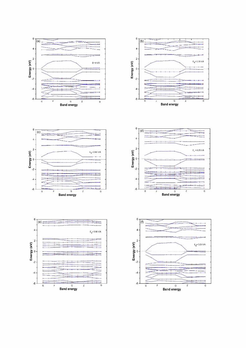
To Applying an 𝐸𝑒𝑥𝑡 is a method to control the energy band gap of 2D-materials. It is very important to
know how the electronic band structures are adjusted by the effects of the 𝐸𝑒𝑥𝑡, applied in (x, y, z) directions
of GO layer. The band structures of GO calculated along high symmetry directions of the Brillouin zone,
are plotted in Fig.2. The band structures show that the conduction band minimum and the valence band
maximum, are located at G and Z points of the Brillouin zone, which indicate that the GO has a direct band
gap. In Fig.3, the band gap energy increases from 0.183 eV to 0.522 eV of the 𝐸𝑒𝑥𝑡 values change from 0
V/Å to 0.50 V/Å, respectively, applied on GO sheet in x direction, by reason of the shift upward of
conduction band, specifically at Z point of the Brillouin zone. The response of band gap energy of GO to
the 𝐸𝑒𝑥𝑡 in x direction, shows a near-linear behavior and facilitates its modulation. In y direction, the band
gap increases from 0.189 eV to 0.719 eV by the effects of the 𝐸𝑒𝑥𝑡 applied on GO from 0 V/Å to 0.50 V/Å
respectively. Additionally, an 𝐸𝑒𝑥𝑡 applied on GO sheet from 0 V/Å to 0.50 V/Å in z direction, lead to
decreases the band gap energy from 0.183 eV to 0.001 eV respectively, by reason of the shift upward in the
valence band, specifically at G point of the Brillouin zone. It can be seen that the 𝐸𝑒𝑥𝑡 lead to shifts the
energy levels of GO material, and this displacement is influenced by the direction of its application.
It is clear from Fig.3, that the GO exhibit the modulation of the band gap by the effects of the 𝐸𝑒𝑥𝑡,
applied in (x, y, z) directions of space. Hence, the results of band gap energy indicate the semiconducting
properties of GO under the 𝐸𝑒𝑥𝑡, and become almost metallic for an 𝐸𝑒𝑥𝑡 value equal to 0.50 V/Å applied
in z direction. The influence of the 𝐸𝑒𝑥𝑡 on the band gap closer to the Fermi level, can be summarized as
follows: For x direction, the conduction band moves upward and the valence band remains almost fixed at
Z point of the Brillouin zone. In y direction, the conduction and valence bands move upward for opening
the band gap. But for z direction, the conduction band moves downward and the valence band remains
almost fixed at Z point of the Brillouin zone, for an 𝐸𝑒𝑥𝑡 value equal to 0.25 V/Å, and the valence band
moves upward and the conduction band remains almost fixed at G point of the Brillouin zone, for an 𝐸𝑒𝑥𝑡
value equal to 0.50 V/Å.
The application of a perturbing potential on GO layer, breaks the symmetry and resulting the mixture of
its electronic states. The amplitude of the 𝐸𝑒𝑥𝑡 should give rise to a significant modulation of the band gap
energy of the GO semiconductor. These results, show an opening and closing of the band gap energy, by
reason of the strength of the 𝐸𝑒𝑥𝑡 applied in (x, y) and z directions, respectively. The effect of an 𝐸𝑒𝑥𝑡 is the
effective method, to control and modulate the electronic property of GO material. This makes GO a
semiconductor with a controllable band gap, which lead to develop the photo detectors devices.
Fig. 2. Band gap energies of GO structure, under an 𝐸𝑒𝑥𝑡 applied in (x, y, z) directions.
Fig.3. Variation of the band gap as a function of the 𝐸𝑒𝑥𝑡, applied on GO layer in (x, y, z) directions.
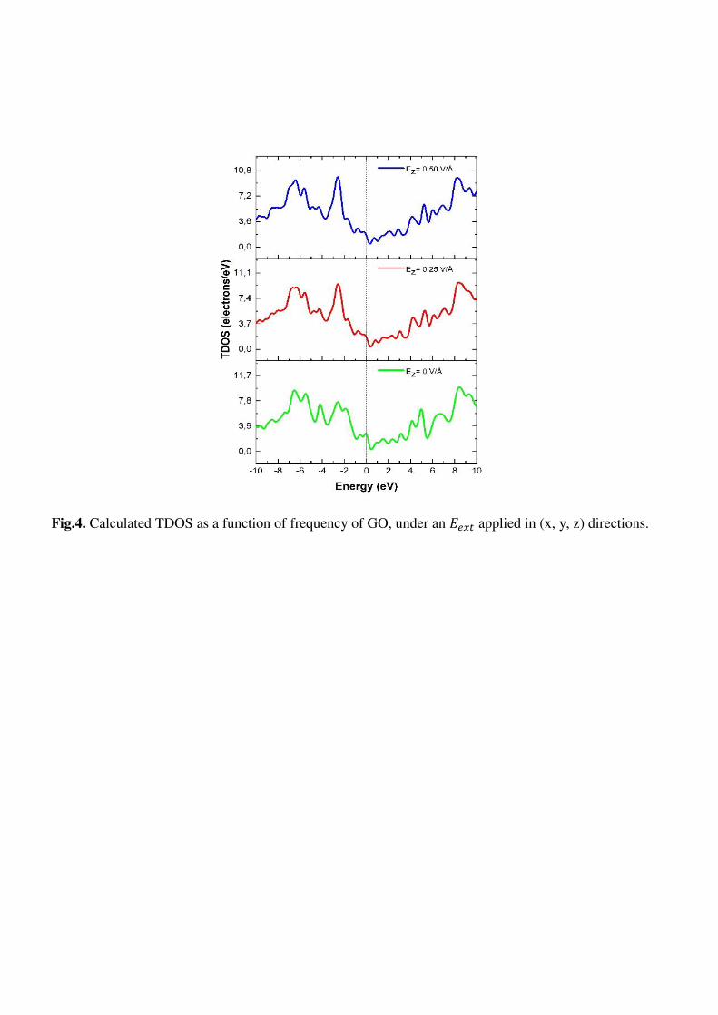
3.1.2 Density of stats
The density of states (DOS) is a quantum property, that is used in solid-state physics. It refers to the number
of allowed electron energy states per unit energy interval, around an energy 𝐸 in a solid crystal. In the
electronic states, the DOS permits the calculation of the number of electrons for each energy level. Most
properties of crystals semiconductors, including their optical and electronic properties are determined by
their DOS. The description of these states, defines the electrical conduction properties of a crystal [15]. The
total density of states (TDOS) and partial density of states (PDOS) of GO layer, are plotted as a function of
the 𝐸𝑒𝑥𝑡, as shown in Fig.4 and Fig.5, respectively. The TDOS near the Fermi level exhibits a small
population, by reason of the semiconductor character of GO material. The probability of occupation
electronic states by the valence electrons, increases around the Fermi level under the effects of the 𝐸𝑒𝑥𝑡
applied in both x and y directions, and decreases by the 𝐸𝑒𝑥𝑡 applied in the z direction of GO layer.
The PDOS, which is essentially the local DOS for each atom in the GO layer, can provide additional
insight into any observed changes in the electronic structure. The states of all atoms in GO sheet around the
Fermi level, primarily originate from 2pz orbitals and we focused on them for plotted the PDOS. The oxygen
atoms loses the electrons while the carbon atoms gains the electrons, under an action of the 𝐸𝑒𝑥𝑡 applied in
z direction. The loss of electrons by oxygen atoms comes from O 2p orbitals, and the gain of electrons by
carbon atoms is attributed to the C 2p orbitals under the effects of the 𝐸𝑒𝑥𝑡. The number of electrons lost by
the oxygen atoms or gained by the carbon atoms, increases by the application of the 𝐸𝑒𝑥𝑡 from 0 V/Å to
0.50 V/Å in z direction. These results clarify the strong effect of the 𝐸𝑒𝑥𝑡 on the electronic properties of GO
material.
Fig.4. Calculated TDOS as a function of frequency of GO, under an 𝐸𝑒𝑥𝑡 applied in (x, y, z) directions.
Fig.5. Calculated PDOS as a function of frequency of GO, under an 𝐸𝑒𝑥𝑡 applied in (x, y, z) directions.
3.2 Optical properties
3.2.1 Absorption
In the present study, we have presented the variation of absorption coefficient α as a function of photon
energy (ℎ𝜈), under an 𝐸𝑒𝑥𝑡 from 0 V/A˚ to 0.50 V/A˚, applied in (x, y, z) directions of GO layer in 0 - 8 eV
range, as shown in Fig.6. For the absence of an 𝐸𝑒𝑥𝑡, the absorption spectrum consists of two peaks with
different intensities. The first peak with low intensity appear at 3.01 eV, and the second peak identified at
5.69 eV [16]. The source of peaks arises from two essential transitions between electronic states of GO.
The first peak corresponds to the transition from occupied n to unoccupied n* state in the conduction bands.
The large second peak corresponds to the transition of π-π* states for C-C bond in sp2 hybrid regions.
According to these two peaks, GO exhibits a powerful light absorption, it can absorb both ultraviolet and
visible light. When the effects of the 𝐸𝑒𝑥𝑡 applied in x direction of GO layer, the intensity of absorption
peaks decreases in both ultraviolet and visible ranges, due to the decrease of the number of electrons and
photo-generated holes under the 𝐸𝑒𝑥𝑡 effects. In y direction, the 𝐸𝑒𝑥𝑡 applied on GO lead to decrease the
intensity of α peaks in the ultraviolet domain, and increase the intensity of α peaks in the visible range. On
the other hand, when the 𝐸𝑒𝑥𝑡 applied in z direction, the intensity of α peaks in ultraviolet range increase of
0.25 V/Å, and decrease of 0.5 V/Å. But, in visible range the α peaks increases, due to the decreases of free
electrons number in GO sheet Table.2.
The application of the 𝐸𝑒𝑥𝑡 in z direction, leads to increase the redshift of the absorption edge, by reason
of the decreases of the band gap energy of GO structure. This result is in agreement with the energy band
gap plotted in Fig.3. Finally, these effects demonstrate that the effects of the 𝐸𝑒𝑥𝑡, can be effectively used
to modify the power absorption of light by GO material. The results of our calculations for the absorption
spectrum, show that the optical properties of GO, are strongly depend on the direction of applied the 𝐸𝑒𝑥𝑡.
The absorption of visible light by the GO material under an 𝐸𝑒𝑥𝑡 applied in z direction, enables to us increase
the light-absorbing capacity, which is essential for photo-induced applications.
Fig. 6. Calculated 𝛼(𝜔) of GO structure, under the 𝐸𝑒𝑥𝑡 applied in (x, y, z) directions.
Table. 2. The 𝛼(𝜔) peaks of GO structures under the 𝐸𝑒𝑥𝑡.
External electric field (V/Å) Ex=0 Ex=0.25 Ex=0.5 Ey=0 Ey=0.25 Ey=0.5 Ez=0 Ez=0.25 Ez=0.5
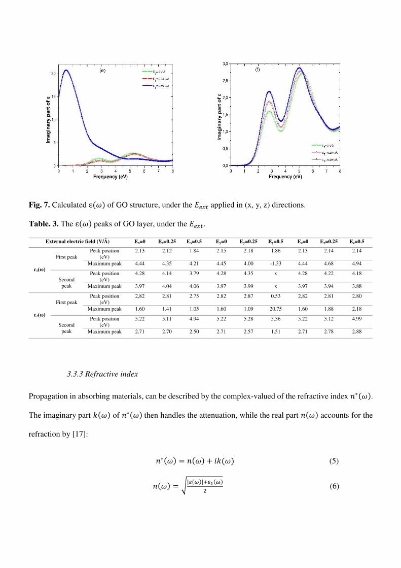
The complex frequency-dependent dielectric function, ɛ(𝜔) can be used to descript the optical properties
of 2D-material, and describes how light interacts when propagating through matter. It determines the
dispersion effects by its real part, ɛ1(𝜔) and the absorption effects by the imaginary part, ɛ2(𝜔). We
measured the energy dependence of GO dielectric function, under the 𝐸𝑒𝑥𝑡 applied in (x, y, z) directions.
The complex dielectric function ɛ(𝜔) is the sum of real and imaginary parts:
𝜀(𝜔) = 𝜀1(𝜔) + 𝑖𝜀2(𝜔) (4)
In the present study, the real and imaginary parts of the GO dielectric function, are calculated in absence
and presence of the effects of the 𝐸𝑒𝑥𝑡, applied in (x, y, z) directions in 0 - 8 eV range, as presented in Fig.7.
At low energies, ɛ(𝜔) is associated with electronic intraband transitions inside the conduction band. In this
spectral range, the optical response is dominated by the free electron behavior. At higher energies, ɛ(𝜔)
reflects the electronic interband transitions. For the 𝐸𝑒𝑥𝑡 increases in x direction of GO layer, the peaks of ɛ1(𝜔) are increase in UV domain and decrease in visible range, which interprets the minimization of the
decomposition of visible light in monochromatic radiations. The peaks concerning the imaginary part ɛ2(𝜔)
are decrease in both UV and visible ranges, under the 𝐸𝑒𝑥𝑡, and these peaks are towards to redshifted. For
y direction, the peaks of ɛ1(𝜔) decrease in both UV and visible ranges, under the effects of the 𝐸𝑒𝑥𝑡, which
interprets the decrease of the dispersion of incident light inside GO material. The peaks which concerning ɛ2(𝜔), decrease for the UV and increase in visible ranges, under the 𝐸𝑒𝑥𝑡. Additionally, for z direction the
peaks of ɛ1(𝜔) decrease in UV range and increase in visible domain, under the 𝐸𝑒𝑥𝑡, which interprets the
increase dispersion of visible light. On the other hand, the peaks of ɛ2(𝜔) increase in both UV and visible
domains under the 𝐸𝑒𝑥𝑡. These results of ɛ2(𝜔) part, shows the remarkable enhanced abilities to absorb
photons by GO material, under the 𝐸𝑒𝑥𝑡 applied in z direction for the visible area Table.3.
The difference between ɛ1(𝜔) values in (x, y, z) directions, suggests that an anisotropic behavior of the
optical properties of GO material, under the 𝐸𝑒𝑥𝑡. For an 𝐸𝑒𝑥𝑡 applied in both x and z directions of GO
structure, ɛ2(𝜔) has two peaks in 2-8 eV range, are always related to the electron excitation. The ɛ2(𝜔)
part, has a low value for the incident photons has the energy (𝐸 = ℎ𝜈) less than 2 eV Fig.7. In addition, it
is noteworthy to say that the value of ɛ1(𝜔) > 0 and ɛ2(𝜔) = 0 in 0-1 eV range, means that this region
transparent. It means that there is no absorption at low energy, because in this case the valence electrons of
GO layer, cannot react fast with the 𝐸𝑒𝑥𝑡, and the transition between the valance band maximum and the
conduction band minimum or between the orbitals is forbidden. Then, under an 𝐸𝑒𝑥𝑡, GO material is an
absorbent material for a wide range of energy, which indicates that this material can be used as an important
element in several optoelectronic devices, such as the transparent conducting films and photovoltaic
devices.
Fig. 7. Calculated ɛ(𝜔) of GO structure, under the 𝐸𝑒𝑥𝑡 applied in (x, y, z) directions.
Table. 3. The ɛ(𝜔) peaks of GO layer, under the 𝐸𝑒𝑥𝑡.
External electric field (V/Å) Ex=0 Ex=0.25 Ex=0.5 Ey=0 Ey=0.25 Ey=0.5 Ez=0 Ez=0.25 Ez=0.5
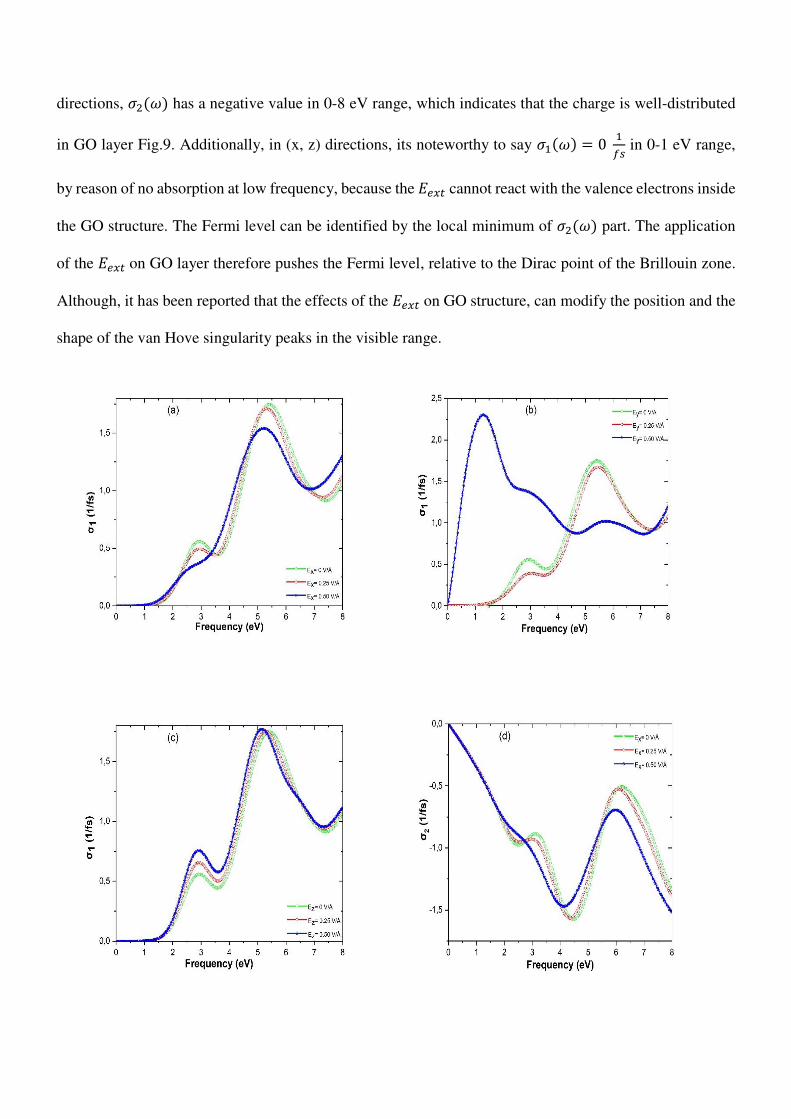
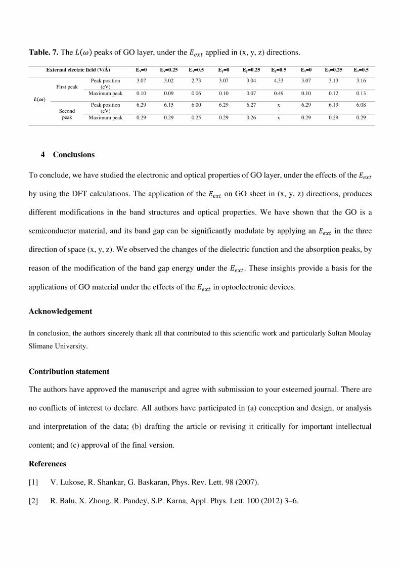
The electron loss function 𝐿(𝜔) describes the energy loss of a fast electron traversing a material, with the
change of frequency. From the real and imaginary parts of ɛ(𝜔), the energy loss function can easily be
obtained by [19]:
𝐿(𝜔) = −𝐼𝑚 ( 1𝜀(𝜔)) = 𝜀2(𝜔)𝜀12(𝜔)+𝜀22(𝜔) (11)
The 𝐿(𝜔) of GO layer under the 𝐸𝑒𝑥𝑡 applied in (x, y, z) directions, shown in Fig.10. The origin of 𝐿(𝜔)
peaks in 0-8 eV range, due to the collective excitations at various photon energies. The 𝐿(𝜔) exhibits two
peaks approximately at 3 and 6 eV, which are associated with the plasma frequency. These two peaks
indicate the maximum energy lost in GO sheet, under the effects of the 𝐸𝑒𝑥𝑡. The application of the 𝐸𝑒𝑥𝑡 on
GO layer in x direction, lead to decrease the peaks of 𝐿(𝜔) in both visible and UV ranges. On the other
hand, the effect of an 𝐸𝑒𝑥𝑡 = 0.25 V/Å applied on GO sheet in y direction, lead to decrease the peaks of 𝐿(𝜔) in both visible and UV ranges. But, the effect of an 𝐸𝑒𝑥𝑡 = 0.50 V/Å lead to increase the peaks of 𝐿(𝜔) in both visible and UV ranges. Additionally, the application of the 𝐸𝑒𝑥𝑡 on GO in z direction, lead to
increase the first peaks of 𝐿(𝜔) in visible range, by reason of the increase the scattering between the incident
visible light and the different particles inside GO structure Table.7. The peaks at 6 eV, due to the energy
lost for π electrons and the peaks at 3 eV are due to the energy lost for π and σ electrons in GO layer, under
an 𝐸𝑒𝑥𝑡 effects. A peak in the 𝐿(𝜔) corresponds to a dip in the ɛ1(𝜔) part, as shown in Fig.7 and Fig.10.
Fig. 10. Calculated 𝐿(𝜔) of GO structure, under the 𝐸𝑒𝑥𝑡 applied in (x, y, z) directions.
Table. 7. The 𝐿(𝜔) peaks of GO layer, under the 𝐸𝑒𝑥𝑡 applied in (x, y, z) directions.
External electric field (V/Å) Ex=0 Ex=0.25 Ex=0.5 Ey=0 Ey=0.25 Ey=0.5 Ez=0 Ez=0.25 Ez=0.5