Page 1
Enhanced active feedback technique with dynamic compensationfor low-dropout voltage regulator
Chia-Min Chen • Chung-Chih Hung
Received: 16 June 2012 / Revised: 28 December 2012 / Accepted: 18 January 2013 / Published online: 31 January 2013
� Springer Science+Business Media New York 2013
Abstract This paper presents a novel frequency com-
pensation technique for a low-dropout (LDO) voltage
regulator. Enhanced active feedback frequency compen-
sation is employed to improve the frequency response. The
proposed LDO is capable of providing high stability for
current loads up to 150 mA with or without loading
capacitors. The proposed LDO voltage regulator provides a
loop bandwidth of 7.8 MHz under light loads and 6.5 MHz
under heavy loads. The maximum undershoot and over-
shoot are 59 and 90 mV, respectively, for changes in load
current within a 200-ns edge time, while the compensation
capacitors only require a total value of 7 pF. This enables
easy integration of the compensation capacitors within the
LDO chip. The proposed LDO regulator was designed
using TSMC 0.35-lm CMOS technology. With an active
area of 0.14 mm2 (including feedback resistors), the qui-
escent current is only 40 lA. The input voltage ranges
from 1.73 to 5 V for a loading current of 150 mA and an
output voltage of 1.5 V. The main advantage of this
approach is the stability of the LDO circuit when external
load capacitors are connected, or even without load
capacitors.
Keywords Low dropout (LDO) voltage regulator �Frequency compensation � Loop stability � Transient
response � Output ripple noise � Power management
1 Introduction
Portable devices require an efficient power management
system to extend battery life. These devices usually employ
multiple on-chip voltage levels, which has led to the
widespread adoption of low dropout (LDO) voltage regu-
lators for electronic devices, such as MP3 players, cellular
phones, and digital cameras [1, 2]. LDO voltage regulators
result in a small voltage drop across the power transistor
and provide a well regulated low-noise voltage. These are
particularly suitable for applications such as RF IC and
audio IC, which require low noise [3, 4]. Another advan-
tage of linear regulators is the low standby current, due to
the absence of switching. In portable devices, a crucial
design consideration is reducing quiescent current to
maximize the lifespan of the battery [5, 6, 7].
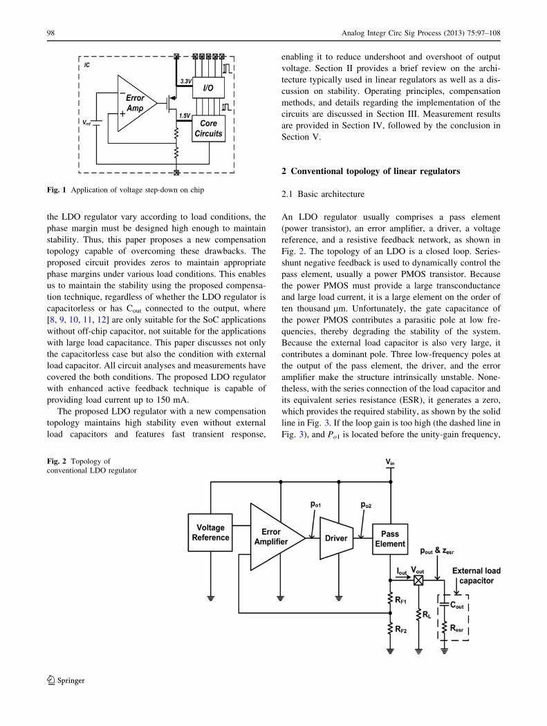
For different applications, LDO regulators are able to
support load current capacity ranging from several hundred
mA to several A. In the design of SoC solutions, a higher
output voltage (e.g., 3.3 V) is usually used for I/O ports,
and a lower voltage (e.g., 1.5 V) is used for digital cores, as
shown in Fig. 1 [8, 9, 10, 11, 12].
Recently, an increasing number of designs have focused
on low supply voltage and low power consumption. A
lower supply voltage is required to decrease power con-
sumption and extend battery life in portable electronic
devices. Conventional LDO error amplifiers must be
designed to provide high gain for precision output voltage
and good regulation. A cascode architecture precludes the
implementation of the amplifier under low supply voltage;
therefore, amplifiers with multiple stages are also usually
required [13]. However, multiple amplification stages
increases the number of poles, which reduces the phase
margin, resulting in stability problems. Moreover, because
the transconductance and resistance of the output stage of
C.-M. Chen � C.-C. Hung (&)
Analog Integrated Circuit Laboratory, Department of Electrical
Engineering, National Chiao Tung University, Hsinchu, Taiwan
e-mail: [email protected]
C.-M. Chen
e-mail: [email protected]
123
Analog Integr Circ Sig Process (2013) 75:97–108
DOI 10.1007/s10470-013-0034-x
Page 2
the LDO regulator vary according to load conditions, the
phase margin must be designed high enough to maintain
stability. Thus, this paper proposes a new compensation
topology capable of overcoming these drawbacks. The
proposed circuit provides zeros to maintain appropriate
phase margins under various load conditions. This enables
us to maintain the stability using the proposed compensa-
tion technique, regardless of whether the LDO regulator is
capacitorless or has Cout connected to the output, where
[8, 9, 10, 11, 12] are only suitable for the SoC applications
without off-chip capacitor, not suitable for the applications
with large load capacitance. This paper discusses not only
the capacitorless case but also the condition with external
load capacitor. All circuit analyses and measurements have
covered the both conditions. The proposed LDO regulator
with enhanced active feedback technique is capable of
providing load current up to 150 mA.
The proposed LDO regulator with a new compensation
topology maintains high stability even without external
load capacitors and features fast transient response,
enabling it to reduce undershoot and overshoot of output
voltage. Section II provides a brief review on the archi-
tecture typically used in linear regulators as well as a dis-
cussion on stability. Operating principles, compensation
methods, and details regarding the implementation of the
circuits are discussed in Section III. Measurement results
are provided in Section IV, followed by the conclusion in
Section V.
2 Conventional topology of linear regulators
2.1 Basic architecture
An LDO regulator usually comprises a pass element
(power transistor), an error amplifier, a driver, a voltage
reference, and a resistive feedback network, as shown in
Fig. 2. The topology of an LDO is a closed loop. Series-
shunt negative feedback is used to dynamically control the
pass element, usually a power PMOS transistor. Because
the power PMOS must provide a large transconductance
and large load current, it is a large element on the order of
ten thousand lm. Unfortunately, the gate capacitance of
the power PMOS contributes a parasitic pole at low fre-
quencies, thereby degrading the stability of the system.
Because the external load capacitor is also very large, it
contributes a dominant pole. Three low-frequency poles at
the output of the pass element, the driver, and the error
amplifier make the structure intrinsically unstable. None-
theless, with the series connection of the load capacitor and
its equivalent series resistance (ESR), it generates a zero,
which provides the required stability, as shown by the solid
line in Fig. 3. If the loop gain is too high (the dashed line in
Fig. 3), and Po1 is located before the unity-gain frequency,
Fig. 2 Topology of
conventional LDO regulator
Fig. 1 Application of voltage step-down on chip
98 Analog Integr Circ Sig Process (2013) 75:97–108
123
Page 3
an even larger load capacitance is required to maintain
stability. This compensation method usually results in a
narrow bandwidth [14, 15].
The LDO regulator operates as a closed loop system,
which requires compensation to ensure stability under all
operating conditions. The fundamental requirements for
stability are: (1) the zero must be located below the unity
gain frequency of the loop; and (2) all high-frequency poles
must be at least three times higher than the unity gain
frequency [16]. However, the ESR values differ according
to the material used in the load capacitors making it very
difficult to accurately control the value of the ESR.
2.2 Existing techniques
One popular compensation method is the Miller compen-
sation technique, as presented in Fig. 4 [17]. This tech-
nique involves connecting a capacitor between the output
and input of the second stage gmII. The poles of the two-
stage amplifier are split, one toward low frequency and the
other toward high frequency. In this manner, the dominant
pole is located at the output node of the first stage. The
dominant low-frequency pole, Pn1, is located at node n1
and is given by
Pn1 �1
ro1 A2Cmð Þ ¼1
ro1 gmIIro2Cmð Þ ð1Þ
where A2 refers to the gain of the second stage. At high
frequencies, the compensation capacitor Cm shunts the
output to node n1, converting the input transistor of
the second stage into a diode connected device. This moves
the output pole toward higher frequencies
Pn2 �gmII
Coutð2Þ
A right-half plane zero also results from the topology
described by (ZRHP = gmII/Cm). This zero is the result of
capacitor Cm providing a noninverting feedforward path,
which degrades the phase margin. Variations in load cause
very wide variations in gmII, and thus in the high frequency
pole (Pn2). Consequently, the Miller capacitor must be very
large to keep the poles separated, which results in a very
large chip area. Other compensation techniques providing
amplification greater than that from the Miller effect are
capable of improving the performance and reducing the
area significantly [18, 19, 20].
3 Proposed LDO regulator
3.1 Architecture
Figure 5 shows the block diagram of the proposed LDO
regulator. The architecture of the proposed error amplifier
is basically a two stage gain amplifier driving the power
transistor. Thus, this LDO regulator can be viewed as a
three stage amplifier driving a capacitive load with a par-
allel resistive load. The first stage is designed as a high gain
error amplifier using a folded cascode topology to enhance
the dynamic range of the input and the output impedance
for higher gain. The first stage provides a gain of approx-
imately 60 dB. An enhanced active feedback (EAF) block
comprises gmk1, gmk2, Ck, Rk. This block utilizes the com-
pensation capacitor Ck by multiplying the gain factors of
two stages (gmII, gmk1) to form a low-frequency pole
(dominant pole for Cout = 0). Compared with traditional
Miller compensation, EAF compensation appears to have
one more gain stage factor, enabling the compensated
capacitance Ck to have a much smaller value. This block
also generates a zero Z1 to cancel the non-dominant pole.
The second stage, which must be able to turn the power
transistor (power PMOS MPO) on and turn off quickly,
provides high signal swing and 25 dB gain. The bias current
of the second stage is proportional to the slew rate, while the
charge time of the power transistor gate is inversely
Fig. 3 Frequency response of conventional LDO regulator
Fig. 4 Two-stage Miller-compensated LDO regulator
Analog Integr Circ Sig Process (2013) 75:97–108 99
123
Page 4
proportional to the parasitic gate capacitance; therefore, the
bias circuit must be carefully designed to enhance overall
efficiency. Capacitor Cm constitutes a fast path capable of
reducing response time. Due to the small value of capacitor
Cm (3 pF), the combination of feed-forward path (FFP) gmf
and the fast path does not produce a right-half plane (RHP)
zero inside the unity-gain frequency to degrade phase
margin. In addition, capacitor Cm pushes the pole of the
second stage output to a lower frequency. The feedforward
stage (gmf) accelerates the transient discharge time of the
output terminal. We have also designed an embedded RC
block (Ct1, Rt1) to add another internal zero compensation to
reduce phase shift at high frequencies.
In Fig. 5, P1(P01) is the dominant pole, contributed by
the output of the first amplifier stage. P2(P02) represents the
second pole, contributed by the output of the second
amplifier stage. P3(P03) is the third pole, contributed by
node n3 of the enhanced active feedback. Z1(Z 01) is the first
LHP zero, generated by the enhanced active feedback
circuit. Z2(Z 02) represents the second LHP zero, generated
by compensation capacitor Ct1 and compensation resistor
Rt1. The pole and zero symbols marked ‘‘0’’ represent the
poles and zeros generated under heavy loads; otherwise,
they refer to light load conditions.
The negative gain of the output stage (power transistor)
depends heavily on the load. The gain of the power tran-
sistor (gmpRop) is inversely proportional toffiffiffiffiffiffiffi
Iout
p. The dis-
tribution of gain among the stages is an important
consideration. To prevent front stages from forwarding
noise, DC gain is distributed such that AV1 [ AV2 [ AVP. A
resistive feedback network was added at the output of the
three stage amplifier to form a negative feedback system.
The feedback resistors must be large enough to reduce
quiescent current for low power design. This architecture
requires a high loop gain to provide high-precision LDO
output voltage.
Fig. 5 Block diagram of the proposed LDO regulator without external load capacitor
Fig. 6 Schematic of the proposed LDO regulator
100 Analog Integr Circ Sig Process (2013) 75:97–108
123
Page 5
3.2 Analysis of stability without external load
capacitor
The circuitry of the proposed LDO regulator is detailed in
Fig. 6. Transistors M1–M8 form the first stage of the error
amplifier while transistors M9–M12 form the second stage.
The dominant pole is contributed by the output of the first
stage. Capacitor Ck, the transconductance of the second
stage gmII, and the gain stage gmk1 introduce the pole-
splitting effect, which pushes the pole of the first stage
output toward very low frequencies, resulting in a new
dominant pole for the system. Meanwhile, the pole pro-
duced by the output node of the negative gain stages gmk1
and gmk2 is pushed toward a higher frequency, resulting in
the third pole of the feedback loop. The feedforward stage
(gmf) reduces the output impedance at the output node of
the LDO regulator. Compensation capacitor Cm splits the
poles at the input and output nodes of the power transistor
Fig. 7 Simulated loop gain and
phase responses of the proposed
LDO regulator under different
loads without external load
capacitor (Cout = 0,
Cop = 100 pF)
Analog Integr Circ Sig Process (2013) 75:97–108 101
123
Page 6
stage. Thus, the pole at the LDO regulator output node is
pushed toward frequencies higher than the unity gain fre-
quency, by the transconductance of the power transistor
and compensation capacitor Cm. The pole at the power
transistor MPO gate node is then pushed toward lower
frequencies, forming the second pole of the feedback loop.
Compensation resistor Rk, compensation capacitor Ck,
negative gain stages gmk1, gmk2, and gmII introduce a first
LHP zero, Z1. The first LHP zero cancels the third pole.
Resistor Rk and capacitor Ck allow independent adjustment
over the placement of the first zero. Resistor Rt1 and
capacitor Ct1 can also introduce a second LHP zero, Z2.
The second LHP zero is presented to improve the phase
margin of the LDO regulator. Resistance Rt1 is the small
signal equivalent resistance of the transistor Mt1. Capacitor
Ct1 also allows independent adjustment over the placement
of the second zero. All of the major zero and pole rela-
tionships are indicated in Fig. 5.
Fig. 8 Simulated loop gain and
phase responses of the proposed
LDO regulator under different
loads using external load
capacitor (Cout = 10 lF,
Resr = 0.1 X)
102 Analog Integr Circ Sig Process (2013) 75:97–108
123
Page 7
Figures 7 and 8 are the simulated loop gain and phase
responses of the proposed LDO regulator under different
loads with different Cout conditions. The frequency
response of the proposed LDO regulator without external
load capacitor is divided into two states: light load and
heavy load, as shown in Fig. 9. The open loop gain transfer
function of the proposed structure is given by
Hðcap�lessÞ sð Þ �ADC 1þ s
z1
� �
1þ sz2
� �
1þ sP�3dB
� �
1þ sp2
� �
1þ sp3
� � ð3Þ
ADC ¼ gmIgmIIgmpRo1Ro2RopRf 2
Rf 1þRf 2
� �
ð4Þ
P�3dB ¼ P1 ¼ P01 ¼1
Ckgmk1gmIIRokRo1Ro2
ð5Þ
P2 ¼ P02
¼ gmIIgmk1
Cmgmpgmk2Rop � Cmgmk1gmf Rop þ Ct1gmIIgmk1Rt1
� �
ð6Þ
P3 ¼ P03 ¼gmk2Ck
Co1Cok þ CkCo1 þ CkCokð7Þ
Z1 ¼ Z 01 ¼gmk2 gmII þ gmk1ð Þ
Ck gmk2 � gmII � gmk1ð Þ � gmk2 gmII þ gmk1ð ÞRk½ �ð8Þ
Z2 ¼ Z 02 ¼1
Ct1Rt1ð9Þ
UGF ¼ UGF0 ¼ gmIgmpRop
Ckgmk1Rok
Rf 2
Rf 1 þ Rf 2
� �
ð10Þ
where gmI, gmII, gmp, Co1, Co2, Cop, Ro1, Ro2, and Rop are the
transconductance, output capacitance and output resistance
of the three stages, respectively. Because Co2 and Cop are
smaller than the other parameters in the derivation process
and are thus neglected, these two symbols do not appear in
the above equations.
The elements gmk1, gmk2, Ck, and Rk represent the trans-
conductance, compensation capacitance, and compensation
Fig. 9 Frequency response of the proposed LDO regulator with
Cout = 0
Fig. 10 Block diagram of the
proposed LDO regulator with
external load capacitor
Fig. 11 Frequency response of the proposed LDO regulator with
Cout = 0
Analog Integr Circ Sig Process (2013) 75:97–108 103
123
Page 8
resistance of the enhanced active feedback block, respec-
tively. The small signal elements Ct1 and Rt1 are the
equivalent capacitance and equivalent resistance of the
embedded RC block. gmf and Cm are the transconductance
of the feedforward stage and the fast path capacitance,
respectively.
The unity gain bandwidth location changes with load
current. When there is no load capacitor, the loop band-
width is larger. This large bandwidth improves signal
transient response at Cout = 0 resulting in fast line transient
and load transient states. The loop bandwidth under light
load is larger than under heavy load, which degrades sta-
bility under light loads. The proposed LDO voltage regu-
lator provides a loop bandwidth of 7.8 MHz under light
loads and 6.5 MHz under heavy loads. Three poles and two
LHP zeros were designed in the loop, as shown in Fig. 9.
Pole-zero cancellation was achieved by Z1 and P3. Z2
reduces phase shift and maintains an adequate phase mar-
gin. Even when heavily loaded, the system still provides
three poles and two zeros, which ensure that stability is
maintained.
3.3 Analysis of stability using external load capacitor
The other situation involves load capacitors at the output
terminal of the LDO regulator. Figure 10 shows the block
diagram of the proposed LDO regulator with external load
capacitor, which also illustrates all of the major zero and
pole relationships. Under light loads, the dominant pole
(P1) is formed by the large load capacitor and the second
pole (P2) is contributed by the output of the first stage,
while the dominant pole (P01) is contributed by the output of
the first stage and the second pole (P02) is formed by the
large load capacitor under heavy loads. The third pole
(P3(P03)) is contributed by the output of the second stage,
the first LHP zero (Z1(Z 01)) is formed by the load capacitor
and the ESR, and the second LHP zero (Z2(Z 02)) is formed
by the EAF circuit. The pole and zero symbols marked ‘‘0’’represent the poles and zeros generated under heavy loads;
otherwise they refer to light load conditions. The transfer
function can be derived, and three poles and two LHP zeros
are shown as follows.
Fig. 12 Microphotograph of the proposed LDO
Fig. 13 Measured load
regulation of the proposed LDO
104 Analog Integr Circ Sig Process (2013) 75:97–108
123
Page 9
ADC ¼ gmIgmIIgmpRo1Ro2RopRf 2
Rf 1þRf 2
� �
ð11Þ
P1 ¼ P02 ¼1
Cout Resr þ Rop
� � ð12Þ
P2 ¼ P01 ¼1
Ckgmk1gmIIRokRo1Ro2
ð13Þ
P3 ¼ P03 ¼gmIIgmk1 Resr þ Rop
� �
Cmgmpgmk2 Resr þ Rop
� �
� Cmgmk1gmf Resr þ Rop
� �
þ Ct1gmIIgmk1Rt1
2
6
4
3
7
5
Rop
ð14Þ
Z1 ¼ Z 01 ¼1
CoutResrð15Þ
Z2 ¼ Z 02 ¼gmk2 gmII þ gmk1ð Þ
Ck gmk2 � gmII � gmk1ð Þ � gmk2 gmII þ gmk1ð ÞRk½ �ð16Þ
UGF ¼ gmIgmIIgmpRo1Ro2Rop
Cout Resr þ Rop
� �
Rf 2
Rf 1 þ Rf 2
� �
ð17Þ
UGF0 ¼ gmIgmpRop
Ckgmk1Rok
Rf 2
Rf 1 þ Rf 2
� �
ð18Þ
When load capacitors are added, the loop bandwidth is
reduced. When the load current is small, the system gen-
erates two low frequency poles and one zero located at a
frequency below the unity-gain frequency. When the load
current increases continuously, the dominant pole P1 shifts
to higher frequency pole P02, and pole P03 show up below
the unity gain frequency. The proposed EAF compensation
network creates one new dominant pole P01 at lower
Fig. 14 Dropout voltage
performance at 150 mA load
current
Fig. 15 Measured line transient response and line regulation with
COP = 100pF Fig. 16 Measured ripple rejection with COP = 100pF
Analog Integr Circ Sig Process (2013) 75:97–108 105
123
Page 10
frequencies and one new zero Z 02 to cancel out pole P03, as
shown in Fig. 11. When Cout = 10 lF, the proposed LDO
voltage regulator provides a loop bandwidth of 71.4 kHz
under light loads and 139 kHz under heavy loads, respec-
tively. Nevertheless, the circuit must still be rendered
carefully to guarantee adequate phase margin to avoid
oscillation and over-ringing instability during supply volt-
age startup or transient state change.
4 Measurement results
The LDO regulator was implemented using TSMC 0.35-
lm standard CMOS technology. Figure 12 shows the die
microphotograph of the proposed LDO regulator, with an
effective die area of 0.14 mm2, including feedback resis-
tors. The output voltage of the regulator is shown in Fig. 13
as the load current is varied from 0 to 150 mA. The output
voltage of the regulator is shown in Fig. 14 as the supply
voltage is varied from 1 to 5 V. The DC load and line
regulation performance of the LDO regulator are
0.187 mV/mA and 2.5 mV/V, respectively. The high loop
gain architecture of the LDO limits error in the output
voltage. The negative feedback of the LDO regulator
adjusts the source-gate voltage of the power PMOS with
the change of load current. A continuous increase in load
current decreases the gate voltage of power PMOS until it
reaches zero, at which point the LDO regulator is unable to
regulate. In this design, dependent on the aspect ratio and
the maximum source-gate voltage of the power PMOS, the
maximum driving capacity of the LDO regulator is larger
than 150 mA.
To characterize the line transient response, a supply
voltage pulsating between 1.8 and 3.8 V was applied to the
input, and the effect at the output was measured. The
results are shown in Fig. 15. Figure 16 demonstrates that
the proposed LDO regulator largely reduces input ripple
noise from 200 to 5 mV at 1 MHz, which corresponds to a
40-fold reduction.
Another important characteristic is the load transient
response. When the load current is rapidly pulsed from 0 to
150 mA and from 150 mA to 0 under capacitor-less con-
ditions, the maximum variations in transient output are 59
and 90 mV, respectively, as shown in Fig. 17. When the
Fig. 18 Measured load transient response with Cout = 1 lF
Fig. 17 Measured load transient response with COP = 100 pF
106 Analog Integr Circ Sig Process (2013) 75:97–108
123
Page 11
regulator output was connected to a 1 lF load capacitor,
the maximum variations in transient output were 37 and
30 mV for a transient load current step between 0 and
150 mA, as shown in Fig. 18. When the regulator output
was connected to a 10 lF load capacitor, the maximum
output recovery times were 17 and 40 ls for a transient
load current step between 0 and 150 mA, as shown in
Fig. 19. The rise/fall time of the 0 to 150 mA load current
pulse was 200 ns.
A summary of the proposed LDO regulator performance
is shown in Table 1. The input voltage ranges from 1.73 to
5 V. The LDO regulator is capable of operating down to
1.73 V with a preset output voltage of 1.5 V. The quiescent
current is only 40 lA. The dropout voltage for the worst
case load current (150 mA) is 230 mV. The power supply
rejection ratio (PSRR) is less than -71 dB for frequencies
up to 100 Hz. The equivalent output noise at 100 Hz is
approximately 3.24 lV ffiffiffiffiffiffiffi
HZp
. Table 2 presents the speci-
fications of the proposed LDO regulator and a comparison
with other published designs. The proposed regulator
achieved performance in maximum load current (150 mA),
quiescent current (40 lA), line regulation (2.5 mV/V), and
Figure of Merit (FOM = 0.01 ps) superior to that afforded
by other designs. A lower FOM implies better transient
response.
5 Conclusion
This paper proposes a novel frequency compensation net-
work design for a low dropout voltage regulator and
measurement data are presented. Stability in the LDO
Fig. 19 Measured load transient response with Cout = 10 lF
Table 1 Summary of the LDO Performance
Supply voltage 1.73–5 V
Output voltage 1.5 V
Max. output current 150 mA
Quiescent current 40 lA
Dropout voltage 230 mV
AVout-transient 59 mV, COP = 100 pF @ DIL = 150 mA
Line regulation 2.5 mV/V
Load regulation 0.187 mV/mA
PSRR -71 dB @ 100 Hz
-69.5 dB @ 1 kHz
-63 dB @10 kHz
Output noise 3.24 lV ffiffiffiffiffiffiffi
HZp
@ 100 Hz
COUT 100 pF (COP)/1 lF/10 lF
Active area 0.14 mm2
Table 2 Comparison with previously published LDO regulators
Parameter [8] [9] [10] This work
Technology 90-nm
CMOS
0.35-^m
CMOS
0.35-fim
CMOS
0.35-nm
CMOS
Pass element PMOS PMOS PMOS PMOS
ILoad (mA) 100 100 50 150
Quiescent current
(IQLuA)
6,000 170 65 40
Dropout coltage
(mV)
300 200 200 230
COP (pF) 600 pF 100 pFa 100 pFa 100 pFa
Response time TR
(ns)b0.54 0.06 0.18 0.039
Load regulation
(mV/mA)
1.8 0.02 -0.56 0.187
Line regulation
(mV/mA)
N.A. 3.3 -23 2.5
FOM (ps)b 32.4 0.102 0.234 0.01
a The estimated maxmimum output capacitance COP = 100 pF from
parasitics and test equipmentsb Adopted from [8], TR = COUT 9 VOUT/ILOAD(Max.) and FOM =
TR 9 IQ/ILOAD(Max.)
Analog Integr Circ Sig Process (2013) 75:97–108 107
123
Page 12
regulator using enhanced active feedback techniques and
embedded RC blocks can be achieved with or without
loading capacitors. The LDO regulator adopts both a
feedforward path and a fast path to achieve fast load
transient responses and small overshoots and undershoots.
The design provides large loop gain to improve line and
load regulation. Compared with previously published LDO
regulators, the proposed approach provides low quiescent
current and high speed transient response as shown in
Table 2. The FOM of this regulator compares favorably to
other published works.
Acknowledgments The authors would like to thank the National
Chip Implementation Center for supporting the chip fabrication. This
work was sponsored by the National Science Council.
References
1. Shi, C., Walker, B. C., Zeisel, E., et al. (2007). A highly inte-
grated power management IC for advanced mobile applications.
IEEE Journal of Solid-State Circuits, 42(8), 1723–1731.
2. Gjanci, J., & Chowdhury, M. H. (2011). A hybrid scheme for on-
chip voltage regulation in system-on-a-chip (SOC). IEEE TransVery Large Scale Integrated System, 19(11), 1949–1959.
3. Huang, W.-J., & Liu, S.-I. (2011). A PSRR-enhanced low-drop-
out regulator. IET Electronics Letters, 47(1), 17–18.
4. Wong, K., & Evans, D. (2006). A 150 mA low noise, high PSRR
low-dropout linear regulator in 0.13 lm technology for RF SoC
applications. In Proceedings IEEE European solid-state circuitsconference (ESSCIRC), Sep 2006, pp. 532–535.
5. Rincon-Mora, G. A., & Allen, P. E. (1998). A low-voltage, low
quiescent current, low drop-out regulator. IEEE Journal of Solid-State Circuits, 33(1), 36–44.
6. Lin, C.-H., Chen, K.-H., & Huang, H.-W. (2009). Low-dropout
regulators with adaptive reference control and dynamic push-pull
techniques for enhancing transient performance. IEEE Transac-tions on Power Electronics, 24(4), 1016–1022.
7. Garimella, A., Rashid, M. W., & Furth, P. M. (2010). Reverse
nested miller compensation using current buffers in a three-stage
LDO. IEEE Transactions on Circuits and Systems Part II:Express Briefs, 57(4), 250–254.
8. Hazucha, P., Karnik, T., Bloechel, B. A., Parsons, C., Finan, D.,
& Borkar, S. (2005). Area-efficient linear regulator with ultra-fast
load regulation. IEEE Journal of Solid-State Circuits, 40(4), 933–
940.
9. Yang, H.-C., Huang, M.-H., & Chen, K.-H. (2008). High-PSR-
bandwidth capacitor-free LDO regulator with 50 lA minimized
load current requirement for achieving high efficiency at light
loads. WSEAS Transactions on Circuits and Systems, 7, 428–437.
10. Milliken, R. J., Silva-Martınez, J., & Sanchez-Sinencio, E.
(2007). Full on-chip CMOS low-dropout voltage regulator. IEEETransactions on Circuits and Systems, 54(9), 1879–1890.
11. Huang, W.-J., & Liu, S.-I. (2008). Capacitor-free low dropout
regulators using nested miller compensation with active resistor
and 1-bit programmable capacitor array. IET Circuits, Devicesand Systems, 2(3), 306–316.
12. Chen, C.-M., & Hung, C.-C. (2011). A fast self-reacting capac-
itor-less low-dropout regulator. In Proceedings of IEEE Euro-pean solid-state circuits conference (ESSCIRC), Helsinki,
Finland, Sep. 2011, pp. 12–16.
13. Ramos, J., & Steyaert, M. (2004). Positive feedback frequency
compensation for low-voltage low-power three-stage amplifier.
IEEE Transactions on Circuits and Systems, 51(10), 1967–1974.
14. Leung, K. N., & Mok, P. K. T. (2003). A capacitor-free CMOS
low-dropout regulator with damping-factor-control frequency
compensation. IEEE Journal of Solid-State Circuits, 38(10),
1691–1701.
15. Hsieh, C.-Y., Yang, C.-Y., & Chen, K.-H. (2010). A low-dropout
regulator with smooth peak current control topology for over-
current protection. IEEE Transactions on Power Electronics,25(6), 1386–1394.
16. Chava, C. K., & Silva-Martinez, J. (2004). A frequency com-
pensation scheme for LDO voltage regulators. IEEE Transactionson Circuits and Systems I, 51(6), 1041–1050.
17. Gray, P. R., Hurst, P. J., Lewis, S. H., & Meyer, R. G. (2001).
Analysis and design of analog integrated circuits (4th edn). New
York: Wiley.
18. Rincon-Mora, G. A. (2000). Active Capacitor multiplier in
Miller-compensation circuits. IEEE Journal of Solid-State Cir-cuits, 35(1), 26–32.
19. Lima, F., Geraldes, A., Marques, T., Ramalho, J. N., & Casimiro,
P. (2003). Embedded CMOS distributed voltage regulator for
large core loads. In Proceedings of European solid-state circuitsconference (ESSCIRC), Sep. 2003, pp. 521–524.
20. Rincon-Mora, G. A. (2009). Analog IC design with low-dropoutregulators. McGraw-Hill Professional: New York.
Chia-Min Chen received the
M.S. degree in electrical engi-
neering from National Chiao
Tung University, Hsinchu,
Taiwan, in 2006. He is currently
working toward the Ph.D.
degree at the Department of
Electrical Engineering, National
Chiao Tung University, Hsin-
chu, Taiwan. His research
interests include mixed-signal
integrated circuit design, power
management integrated circuits,
and energy-efficient integrated
circuits and systems.
Chung-Chih Hung received the
B.S. degree in electrical engi-
neering from National Taiwan
University, Taipei, Taiwan, in
1989, and the M.S. and Ph.D.
degrees in electrical engineering
from The Ohio State University,
Columbus, Ohio, in 1993 and
1997, respectively. From 1997
to 2003, he worked for several
IC design companies in San
Jose, CA and San Diego, CA,
where he held analog circuit
design manager and director
positions. Since 2003, he has
been with National Chiao Tung University, Hsinchu, Taiwan, where
he is currently a Full Professor in the Department of Electrical
Engineering. His research interests include the design of analog and
mixed-signal integrated circuits for communication and high-speed
applications.
108 Analog Integr Circ Sig Process (2013) 75:97–108
123