Enhanced bandwidth and reduced dispersion through stacking multiple optical metamaterials
Matthew D. Escarra,1,*
Sukosin Thongrattanasiri,2 William O. Charles,
1
Anthony J. Hoffman,1 Viktor A. Podolskiy,
3 and Claire Gmachl
1
1 Department of Electrical Engineering, Princeton University, Princeton, NJ 08544, USA 2 Department of Physics, Oregon State University, Corvallis, OR 97331, USA
3 Department of Physics and Applied Physics, University of Massachusetts Lowell, Lowell, MA 01854, USA *[email protected]
Abstract: All-semiconductor, highly anisotropic metamaterials provide a straightforward path to negative refraction in the mid-infrared. However, their usefulness in applications is restricted by strong frequency dispersion and limited spectral bandwidth. In this work, we show that by stacking multiple metamaterials of varying thickness and doping into one compound metamaterial, bandwidth is increased by 27% over a single-stack metamaterial, and dispersion is reduced.
1. N. Fang, H. Lee, C. Sun, and X. Zhang, “Sub-diffraction-limited optical imaging with a silver superlens,” Science 308(5721), 534–537 (2005).
2. B. D. F. Casse, W. T. Lu, Y. J. Huang, E. Gultepe, L. Menon, and S. Sridhar, “Super-resolution imaging using a three-dimensional metamaterials nanolens,” Appl. Phys. Lett. 96(2), 023114 (2010).
3. A. J. Hoffman, V. A. Podolskiy, D. L. Sivco, and C. Gmachl, “Sub-diffraction negative and positive index modes in mid-infrared waveguides,” Opt. Express 16(21), 16404–16409 (2008).
4. J. Valentine, J. Li, T. Zentgraf, G. Bartal, and X. Zhang, “An optical cloak made of dielectrics,” Nat. Mater. 8(7), 568–571 (2009).
5. Y. A. Urzhumov, N. B. Kundtz, D. R. Smith, and J. B. Pendry, “Cross-section comparisons of cloaks designed by transformation optical and optical conformal mapping approaches,” J. Opt. 13(2), 024002 (2011).
6. G. Dolling, C. Enkrich, M. Wegener, C. M. Soukoulis, and S. Linden, “Low-loss negative-index metamaterial at telecommunication wavelengths,” Opt. Lett. 31(12), 1800–1802 (2006).
7. A. J. Hoffman, L. Alekseyev, S. S. Howard, K. J. Franz, D. Wasserman, V. A. Podolskiy, E. E. Narimanov, D. L. Sivco, and C. Gmachl, “Negative refraction in semiconductor metamaterials,” Nat. Mater. 6(12), 946–950 (2007).
8. S. P. Burgos, R. de Waele, A. Polman, and H. A. Atwater, “A single-layer wide-angle negative-index metamaterial at visible frequencies,” Nat. Mater. 9(5), 407–412 (2010).
9. V. A. Podolskiy and E. E. Narimanov, “Strongly anisotropic waveguide as a nonmagnetic left-handed system,” Phys. Rev. B 71(20), 201101 (2005).
10. A. J. Hoffman, A. Sridhar, P. X. Braun, L. Alekseyev, S. S. Howard, K. J. Franz, L. W. Cheng, F. S. Choa, D. L. Sivco, V. A. Podolskiy, E. E. Narimanov, and C. Gmachl, “Midinfrared semiconductor optical metamaterials,” J. Appl. Phys. 105(12), 122411 (2009).
11. V. G. Veselago, “The electrodynamics of substances with simultaneously negative values of ε and μ,” Sov. Phys. Usp. 10(4), 509–514 (1968).
12. L. V. Alekseyev and E. Narimanov, “Slow light and 3D imaging with non-magnetic negative index systems,” Opt. Express 14(23), 11184–11193 (2006).
13. M. Born and E. Wolf, Principles of Optics (Cambridge University Press, 1997). 14. D. W. Berreman, “Optics in stratified and anisotropic media: 4x4-matrix formulation,” J. Opt. Soc. Am. 62(4),
502–510 (1972). 15. R. M. A. Azzam and N. M. Bashara, Ellipsometry and Polarized Light (North-Holland Pub. Co., 1977). 16. P. Yeh, A. Yariv, and C. S. Hong, “Electromagnetic propagation in periodic stratified media. I. General theory,”
J. Opt. Soc. Am. 67(4), 423–438 (1977). 17. M. Schubert, “Polarization-dependent optical parameters of arbitrarily anisotropic homogeneous layered
systems,” Phys. Rev. B Condens. Matter 53(8), 4265–4274 (1996).
#147613 - $15.00 USD Received 16 May 2011; revised 6 Jul 2011; accepted 6 Jul 2011; published 20 Jul 2011(C) 2011 OSA 1 August 2011 / Vol. 19, No. 16 / OPTICS EXPRESS 14990
1. Introduction
Optical metamaterials have drawn considerable interest in recent years due to their potential for sub-wavelength imaging [1,2], novel waveguiding [3], optical cloaking [4,5], and many other fascinating new applications. More generally, the synthetic nature of these materials allows for significant engineering of their optical response, allowing great creativity in designing new optical materials that have functionalities not found in nature, such as negative refraction [6–8]. However, metamaterials that depend on resonant behavior in their electric permittivity and/or magnetic permeability to achieve their unique properties are limited by the narrow bandwidth and strong dispersion inherent in this resonant behavior.
Recently demonstrated, all-semiconductor, mid-infrared metamaterials show much promise due to their relative low absorption loss, 3-D nature, and straightforward fabrication [7]. These metamaterials feature strong anisotropy in their dielectric response, allowing for negative refraction with only a resonance in their permittivity and not also a resonance in their permeability. While this single-resonance condition leads to reduced loss and simpler construction, it still limits the spectral bandwidth of negative refraction and leads to large dispersion in this negative refraction spectral region, inhibiting the suitability of these materials for applications involving wide-band signals, such as imaging. In an effort to overcome these limitations, the work reported here demonstrates that these layered semiconductor metamaterials can be engineered for broader bandwidth and reduced dispersion in their negative refraction optical response, by forming composite structures of multiple-metamaterial stacks.
2. Design of compound, multiple-stack metamaterials
These mid-infrared metamaterials consist of alternating layers of highly n-doped InGaAs and intrinsic AlInAs. The thickness of each of these layers is strongly sub-wavelength, approximately 100 times smaller than the wavelengths experiencing negative refraction. This alternating of semi-metallic InGaAs layers (with a plasma resonance of free carriers) with undoped AlInAs layers forms a metamaterial with a strongly anisotropic (hyperbolic) dielectric response. The metamaterial exhibits negative refraction for transverse magnetic (TM) polarized light at any non-zero incident angle over a range of wavelengths [7,9].
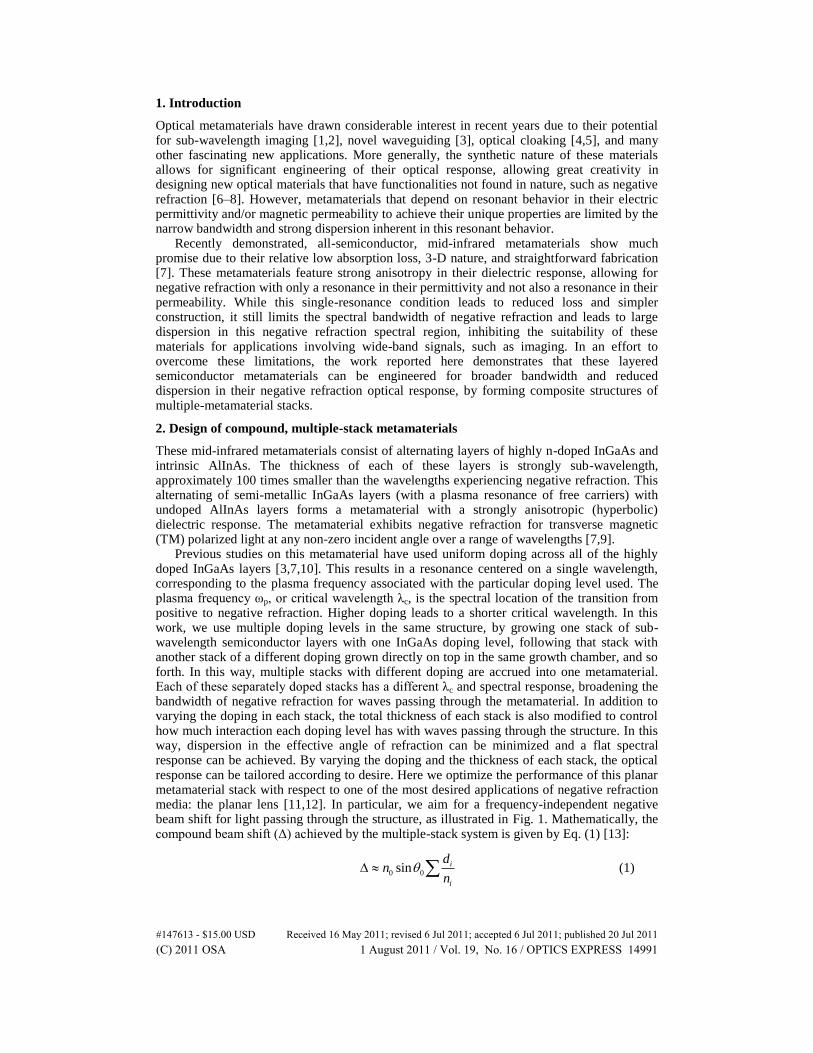
Previous studies on this metamaterial have used uniform doping across all of the highly doped InGaAs layers [3,7,10]. This results in a resonance centered on a single wavelength, corresponding to the plasma frequency associated with the particular doping level used. The plasma frequency ωp, or critical wavelength λc, is the spectral location of the transition from positive to negative refraction. Higher doping leads to a shorter critical wavelength. In this work, we use multiple doping levels in the same structure, by growing one stack of sub-wavelength semiconductor layers with one InGaAs doping level, following that stack with another stack of a different doping grown directly on top in the same growth chamber, and so forth. In this way, multiple stacks with different doping are accrued into one metamaterial. Each of these separately doped stacks has a different λc and spectral response, broadening the bandwidth of negative refraction for waves passing through the metamaterial. In addition to varying the doping in each stack, the total thickness of each stack is also modified to control how much interaction each doping level has with waves passing through the structure. In this way, dispersion in the effective angle of refraction can be minimized and a flat spectral response can be achieved. By varying the doping and the thickness of each stack, the optical response can be tailored according to desire. Here we optimize the performance of this planar metamaterial stack with respect to one of the most desired applications of negative refraction media: the planar lens [11,12]. In particular, we aim for a frequency-independent negative beam shift for light passing through the structure, as illustrated in Fig. 1. Mathematically, the compound beam shift (Δ) achieved by the multiple-stack system is given by Eq. (1) [13]:
0 0sin i
i
dn
n (1)
#147613 - $15.00 USD Received 16 May 2011; revised 6 Jul 2011; accepted 6 Jul 2011; published 20 Jul 2011(C) 2011 OSA 1 August 2011 / Vol. 19, No. 16 / OPTICS EXPRESS 14991
with n0 being the index of the surrounding media, 0 being the incident angle, di being the
thickness of the i-th stack and ni being its effective group index, related to the effective permittivities of the i-th stack via Eq. (2) [10]:
2
|| || 2 2
|| 0 02
||
sinin n
(2)
To demonstrate this effect, three structures were designed, grown, and characterized: a baseline single-stack metamaterial, a two-stack metamaterial, and a four-stack metamaterial. These metamaterials were grown back-to-back by molecular beam epitaxy (MBE) on undoped InP substrates. Each stack consists of 80 nm thick highly Si doped InGaAs layers interleaved with 80 nm thick undoped AlInAs layers. The In0.53Ga0.47As and Al0.48In0.52As layer compositions are lattice-matched to the InP substrate.
The baseline, single stack metamaterial consists of 75 periods of interleaved
InGaAs/AlInAs layers, with InGaAs layers doped at 8.3×10¹⁸
cm3
, for a total epitaxial layer thickness of 12.0 μm. For the two-stack metamaterial, the first stack grown on the InP
substrate consists of 12 periods (1.92 μm thick) with InGaAs layers doped at 7.5×10¹⁸
cm3
, and the second stack grown consists of 60 periods (9.6 μm thick) with InGaAs layers doped at
8.3×10¹⁸
cm3
. For the four-stack metamaterial, the first stack grown contains 6 periods (0.96
μm thick) with InGaAs layers doped at 6.4×10¹⁸
cm3
, the second contains 7 periods (1.12 μm
thick) with InGaAs layers doped at 6.8×10¹⁸
cm3
, the third contains 13 periods (2.08 μm
thick) with InGaAs layers doped at 7.5×10¹⁸
cm3
, and the fourth contains 50 periods (8 μm
thick) with InGaAs layers doped at 8.3×10¹⁸
cm3
. These design values are summarized in Table 1. The table is structured in relation to the InP substrate (bottom row) upon which the stacks are grown.
Table 1. Design Values for a Baseline (Single-Stack) and Two Multi-Stack Samples
Single-Stack Material Two-Stack Material Four-Stack Material
Stack 4 50 periods 8.3×1018 cm-3
Stack 3 13 periods 7.5×1018 cm-3
Stack 2 60 periods 8.3×1018 cm-3 7 periods 6.8×1018 cm-3
Stack 1 75 periods 8.3×1018 cm-3 12 periods 7.5×1018 cm-3 6 periods 6.4×1018 cm-3
InP Substrate
These doping and thickness values were chosen by simulating the expected behavior of these materials. Our experimental studies show that the permittivity of the highly doped InGaAs layers is well described by the Drude model, according to Eq. (3) [7,10]:
2
2( ) 1
/
p
InGaAs InGaAsi
(3)
where InGaAs = 12.15 is the isotropic permittivity (at high frequencies) for InGaAs with no
doping, ω is the frequency of interacting light, and τ = 1×10¹³
s is the electron scattering
time. The plasma frequency is given by 2 *n q mp d InGaAs , where nd is the free carrier
density, q is the charge of an electron, and m* = 0.042m0 is the effective mass of an electron in lattice-matched In0.53Ga0.47As. The permittivity of the undoped AlInAs layers is given by
AlInAs = AlInAs = 10.23 [10].
By using a transfer matrix method to compute the coefficients of full electromagnetic waves propagating through each of the stacks [14–17], the beam shift (the distance light translates in the plane of the stacks as it passes through the sample) was calculated versus wavelength, as shown in Fig. 1 for TM light with 5° incident angle. These simulations reveal
#147613 - $15.00 USD Received 16 May 2011; revised 6 Jul 2011; accepted 6 Jul 2011; published 20 Jul 2011(C) 2011 OSA 1 August 2011 / Vol. 19, No. 16 / OPTICS EXPRESS 14992
the expected bandwidth and flatness of the response in the negative refraction (negative shift) region for each structure. The values in Table 1 were chosen to increase the bandwidth and optimize the flatness of the negative beam shift in these simulations for the multi-stack samples as compared to the baseline sample, correcting for chromatic aberration in the conventional metamaterial. From this plot, one can see that the multi-stack metamaterials have a broader and flatter negative refraction response, with the four-stack material having the broadest and flattest response of the three.
Fig. 1. Calculated beam shift of transmitted light vs. wavelength for a baseline metamaterial, two stack metamaterial, and four stack metamaterial. The stacked metamaterials have enhanced bandwidth of negative refraction and reduced dispersion in that region. Inset: Illustration of a two stack metamaterial, where blue and pink represent regions with different doping in the InGaAs (darker) layers. The black and red arrows represent two possible beam paths through this material, for different wavelengths, that result in the same beam shift Δ.
Fabrication of these materials consists entirely of epitaxial growth by MBE or metal organic chemical vapor deposition (MOCVD), which are standard industrial tools for semiconductor manufacturing. There are no lithography steps, metallization steps, or other steps that require a cleanroom environment. For transmission measurements, the substrate side of the samples is mirror polished.
3. Material characterization and analysis
3.1 Initial wafer characterization: XRD and SIMS
The first characterization step for these materials was to confirm good wafer growth quality. This was done through x-ray diffraction (XRD) measurements on the epitaxial layer of each sample. All three showed sharp, periodic diffraction peaks, indicative of high quality growth.
To further establish the accuracy of the growth relative to the design, secondary ion mass spectrometry (SIMS) measurements were performed on each of the three samples, quantifying the Si, Al, Ga, and In atom concentrations versus depth in the growth direction. These SIMS measurements revealed one, two, and four distinct regions with different Si atom density in the InGaAs layers, for the one-, two-, and four-stack samples, respectively. The most critical variable to achieving a broadband, flat-response metamaterial is accurate free carrier doping levels in each stack. In order to extract free carrier density from SIMS-measured Si atom density, the conversion efficiency of Si atoms to free electrons must be determined. This is found by assuming that the experimentally measured λc for the multi-stack materials is determined by the free carrier density of the highest doped stack. Once λc is known (via optical measurements in Sections 3.2 and 3.3), the free carrier density nd can be extracted according to the corresponding plasma frequency ωp. The ratio of this free carrier density to the measured SIMS concentration of Si atoms in the highest doped stack provides the needed conversion efficiency. This can then be applied to the other SIMS-measured Si concentrations to approximate the free carrier concentrations in each stack. This analysis was performed on all three grown samples; the extracted free carrier concentrations are shown in Table 2. This
#147613 - $15.00 USD Received 16 May 2011; revised 6 Jul 2011; accepted 6 Jul 2011; published 20 Jul 2011(C) 2011 OSA 1 August 2011 / Vol. 19, No. 16 / OPTICS EXPRESS 14993
table is again structured in relation to the InP substrate (bottom row) upon which the stacks are grown.
Table 2. Measured Free Carrier Density in the InGaAs Layers
Single-Stack Material Two-Stack Material Four-Stack Material
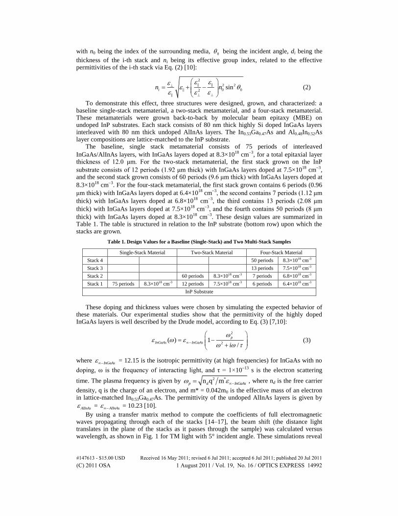
As is evident, the measured doping levels in each stack are somewhat higher than the design values. Even more importantly, the relative difference between doping levels has changed, which changes the relative beam shift for the different stacks – this could have the effect of making the material even more dispersive or could even introduce a positive refraction region within the negative refraction spectral window. With this measured doping data, we can recalculate the beam shift versus wavelength for each sample, again using the transfer matrix method. The results are plotted in Fig. 2. We see that even with the measured doping differing from the design values, the multiple-stack materials are still expected to have reduced dispersion and a wider range of wavelengths that experience negative refraction.
Fig. 2. Re-calculated beam shift vs. wavelength using measured doping values for a baseline metamaterial and two multi-stack metamaterials. The stacked metamaterials still have enhanced bandwidth and reduced dispersion in the negative refraction spectral region.
3.2 Transmission measurements
In order to experimentally observe the macroscopic electromagnetic properties for each of these three metamaterials, the optical transmission and reflection were characterized. This behavior was measured for different polarizations, wavelengths, and incident angles of incoming light. A Fourier-transform infrared (FTIR) spectrometer with a glow bar as a broadband mid-infrared source was used for measuring the wavelength dependence of transmission and reflection. A KRS-5 (TlBr0.4I0.6) wire-grid polarizer was used to choose between TM and transverse electric (TE) polarization. Light was focused into a small spot on the sample with a ZnSe lens so that, for a typical sample size (~a quarter or half of a 2” wafer), the entire beam passed through or was reflected by the sample, even for high incidence angles (up to ~72°). Without the use of an aperture, an incident angle spread of ~8° exists due to this focusing. Light was detected by a liquid nitrogen cooled MCT (HgCdTe) detector. The sample and detector orientation were controlled by mechanized stages for precise selection of the incident angle between incoming light and the sample's surface.
For the transmission measurements, the detector was configured collinearly to collect light after it had passed through the sample. Each measurement was averaged over 100 scans to
reduce noise, and a spectral resolution of 4 cm1
was used. The sample was rotated such that
#147613 - $15.00 USD Received 16 May 2011; revised 6 Jul 2011; accepted 6 Jul 2011; published 20 Jul 2011(C) 2011 OSA 1 August 2011 / Vol. 19, No. 16 / OPTICS EXPRESS 14994
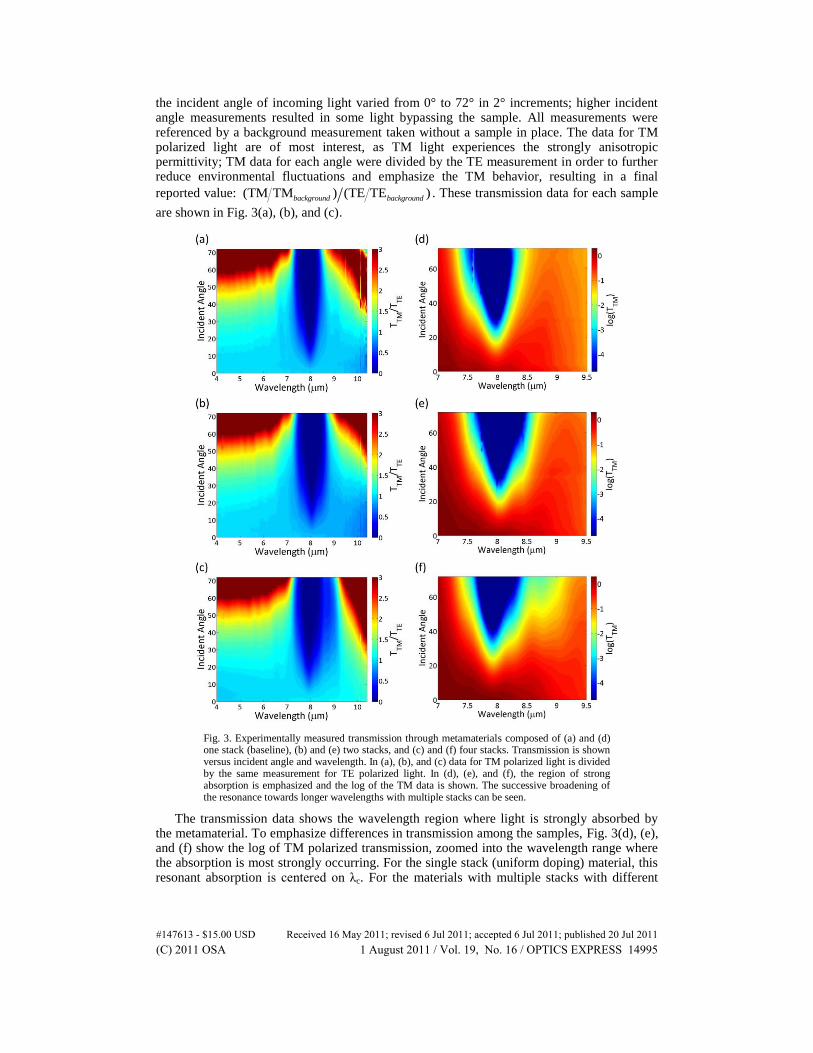
the incident angle of incoming light varied from 0° to 72° in 2° increments; higher incident angle measurements resulted in some light bypassing the sample. All measurements were referenced by a background measurement taken without a sample in place. The data for TM polarized light are of most interest, as TM light experiences the strongly anisotropic permittivity; TM data for each angle were divided by the TE measurement in order to further reduce environmental fluctuations and emphasize the TM behavior, resulting in a final
reported value: (TM TM ) (TE TE )background background. These transmission data for each sample
are shown in Fig. 3(a), (b), and (c).
Fig. 3. Experimentally measured transmission through metamaterials composed of (a) and (d) one stack (baseline), (b) and (e) two stacks, and (c) and (f) four stacks. Transmission is shown versus incident angle and wavelength. In (a), (b), and (c) data for TM polarized light is divided by the same measurement for TE polarized light. In (d), (e), and (f), the region of strong absorption is emphasized and the log of the TM data is shown. The successive broadening of the resonance towards longer wavelengths with multiple stacks can be seen.
The transmission data shows the wavelength region where light is strongly absorbed by the metamaterial. To emphasize differences in transmission among the samples, Fig. 3(d), (e), and (f) show the log of TM polarized transmission, zoomed into the wavelength range where the absorption is most strongly occurring. For the single stack (uniform doping) material, this resonant absorption is centered on λc. For the materials with multiple stacks with different
#147613 - $15.00 USD Received 16 May 2011; revised 6 Jul 2011; accepted 6 Jul 2011; published 20 Jul 2011(C) 2011 OSA 1 August 2011 / Vol. 19, No. 16 / OPTICS EXPRESS 14995
doping levels, multiple absorption dips and shoulders are seen. These absorption features are weighted by the thickness of each stack, as expected from design. These transmission data reveal that the additional stacks have higher critical wavelengths, which corresponds with the designed lower doping levels. The transmission data also show that these different λc are close enough to create a single broadband spectral feature, which favors a single region of negative refraction as opposed to separate regions of negative refraction for the separately doped stacks.
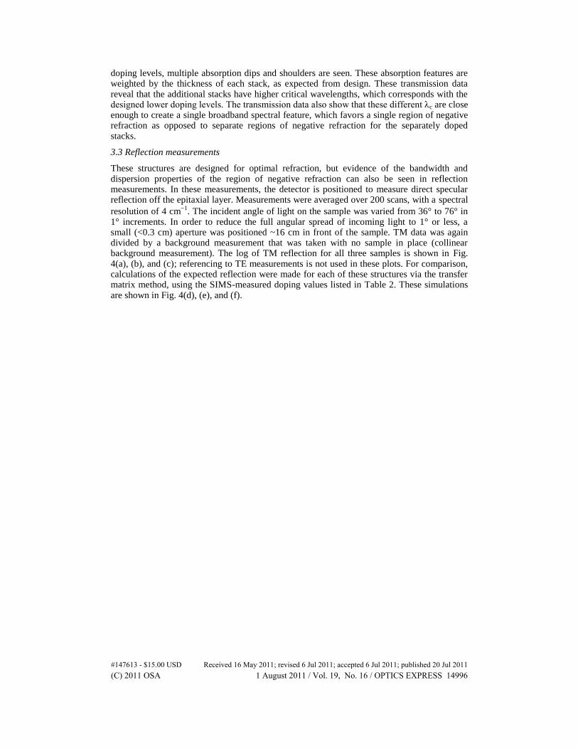
3.3 Reflection measurements
These structures are designed for optimal refraction, but evidence of the bandwidth and dispersion properties of the region of negative refraction can also be seen in reflection measurements. In these measurements, the detector is positioned to measure direct specular reflection off the epitaxial layer. Measurements were averaged over 200 scans, with a spectral
resolution of 4 cm1
. The incident angle of light on the sample was varied from 36° to 76° in 1° increments. In order to reduce the full angular spread of incoming light to 1° or less, a small (<0.3 cm) aperture was positioned ~16 cm in front of the sample. TM data was again divided by a background measurement that was taken with no sample in place (collinear background measurement). The log of TM reflection for all three samples is shown in Fig. 4(a), (b), and (c); referencing to TE measurements is not used in these plots. For comparison, calculations of the expected reflection were made for each of these structures via the transfer matrix method, using the SIMS-measured doping values listed in Table 2. These simulations are shown in Fig. 4(d), (e), and (f).
#147613 - $15.00 USD Received 16 May 2011; revised 6 Jul 2011; accepted 6 Jul 2011; published 20 Jul 2011(C) 2011 OSA 1 August 2011 / Vol. 19, No. 16 / OPTICS EXPRESS 14996
Fig. 4. Natural log of reflection of TM polarized light from metamaterials composed of (a) and (d) one stack (baseline), (b) and (e) two stacks, and (c) and (f) four stacks. Experimentally measured data is shown in (a), (b), and (c). Simulated data is shown in (d), (e), and (f). A trace of the Brewster angle vs. wavelength is overlaid onto each plot (white line).
In each of these data sets, the Brewster angle is traced by a white line. A discontinuity in the Brewster angle occurs at the critical wavelength λc, corresponding to the onset of negative refraction. This is a characteristic feature of TM polarized light in a strongly anisotropic metamaterial [7]. This discontinuity, as well as the dip in transmission shown in Section 3.2, signifies the short-wavelength limit of the spectral region of negative refraction at λc. The long-wavelength limit of the region of negative refraction, designated λmax, corresponds with the wavelength at which the material becomes highly reflective. This was taken to be the point at which the ratio of reflected TM/TE light was greater than 50% of its peak value for an incident angle of 50°. By determining λc and λmax experimentally, we can extract the bandwidth Δλ of each sample according to Eq. (4):
max c
max c 2
(4)
The baseline sample showed a bandwidth of 26.2%, which is similar to previously reported values for this metamaterial [7]. For the multi-stack metamaterials, the two-stack material had a bandwidth of 32.0% and the four-stack material had a bandwidth of 33.2%.
#147613 - $15.00 USD Received 16 May 2011; revised 6 Jul 2011; accepted 6 Jul 2011; published 20 Jul 2011(C) 2011 OSA 1 August 2011 / Vol. 19, No. 16 / OPTICS EXPRESS 14997
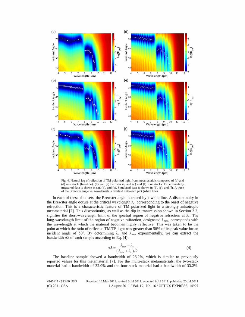
The relative increase in bandwidth is 27% from a baseline metamaterial to a four-stack compound metamaterial.
Fig. 5. The Brewster angle vs. wavelength for a baseline and two multi-stack metamaterials. (a) Shows experimentally measured data and (b) shows transfer matrix calculations.
It is also important to consider the change in the Brewster angle with wavelength. These data are plotted in Fig. 5(a) for the measurements and in Fig. 5(b) for the simulations. There is good agreement between the experimental and simulated data in the Brewster angle in both the positive refraction regime at wavelengths below the discontinuity and in the negative refraction regime for wavelengths higher than the discontinuity. The spectral locations of shifts in the Brewster angle also show good agreement for each metamaterial, with only the critical wavelength λc used as a fitting parameter. This correlation between the experimentally measured data and simulated data for each sample further validates our model. The model that incorporates the SIMS-measured doping shows a flattened response in the negative refraction region for the multi-stack samples (Fig. 2). We therefore conclude that this stacked metamaterial approach successfully reduces dispersion in the negative refraction spectral region.
4. Conclusion
We have proposed and demonstrated a new metamaterial design that enhances bandwidth and reduces dispersion in the wavelength region of interest. This is accomplished by forming a compound, multiple-stack metamaterial, where the free carrier concentration and thickness of each stack is uniquely tailored. This multi-stack metamaterial shows a 27% increase in the bandwidth of the negative refraction spectral region. Furthermore, comparison of the Brewster angle data between our measured samples and simulations further validates our model and indicates that dispersion in this negative refraction spectral region has been reduced. This flatter, broader region of negative refraction makes these materials more aptly suited to applications involving wideband signals, such as imaging. More fundamentally, we show that refraction in these materials can be engineered to take on specified behavior according to design. This engineering can be done through straightforward modification of the growth parameters, without the need for additional complex fabrication techniques. Much potential remains to creatively manipulate the optical response of these materials.
Acknowledgments
The SIMS measurements were performed by Evans Analytical Group® (EAG). This work is supported in part by NSF-ECCS (grant #0724763), NSF-MRSEC PCCM (DMR-0819860), AFOSR (grant #FA9550-09-1-0029), and MIRTHE (NSF-ERC #EEC-0540832).
#147613 - $15.00 USD Received 16 May 2011; revised 6 Jul 2011; accepted 6 Jul 2011; published 20 Jul 2011(C) 2011 OSA 1 August 2011 / Vol. 19, No. 16 / OPTICS EXPRESS 14998