Enhanced metal-insulator transition in freestanding VO2 down to 5 nm thickness Kun Han 1,2, † , Liang Wu 1,3, † * , Yu Cao 4, † , Hanyu Wang 5 , Chen Ye 1 , Ke Huang 1 , M. Motapothula 6,7 , Hongna Xing 8 , Xinghua Li 8 , Dong-Chen Qi 9 , Xiao Li 5 , X. Renshaw Wang 1,10,* 1 Division of Physics and Applied Physics, School of Physical and Mathematical Sciences, Nanyang Technological University, 21 Nanyang Link,637371, Singapore 2 Key Laboratory of Structure and Functional Regulation of Hybrid Materials of Ministry of Education, Institutes of Physical Science and Information Technology, Anhui University, Hefei 230601, China 3 School of Material Science and Engineering, Kunming University of Science and Technology, Kunming, Yunnan 650093, China 4 Department of Electrical and Computer Engineering, National University of Singapore, 4 Engineering Drive 3, Singapore 117583 5 NNU-SULI Thermal Energy Research Center, Center for Quantum Transport and Thermal Energy Science (CQTES), School of Physics and Technology, Nanjing Normal University, Nanjing 210023, China 6 Department of Physics and Astronomy, Uppsala University, Box 516, SE-75120 Uppsala, Sweden 7 Department of Physics, SRM University AP, Amaravati, Andhra Pradesh 522-502, India 8 School of Physics, Northwest University, Xi’an 710069, China 9 Centre for Materials Science, School of Chemistry and Physics, Queensland University of Technology, Brisbane, QLD 4001, Australia 10 School of Electrical and Electronic Engineering, Nanyang Technological University, 50 Nanyang Ave, 639798, Singapore † These authors contributed equally *e-mail: [email protected], [email protected]Keywords: Vanadium Dioxide, Metal-insulator transition, Freestanding membrane, Flexible electronics, Sr3Al2O6
Transcript
Enhanced metal-insulator transition in freestanding VO2
down to 5 nm thickness
Kun Han1,2, †, Liang Wu1,3, † *, Yu Cao4, †, Hanyu Wang5, Chen Ye1, Ke Huang1, M. Motapothula6,7, Hongna Xing8, Xinghua Li8, Dong-Chen Qi9, Xiao Li5, X. Renshaw Wang1,10,* 1Division of Physics and Applied Physics, School of Physical and Mathematical Sciences, Nanyang Technological University, 21 Nanyang Link,637371, Singapore
2Key Laboratory of Structure and Functional Regulation of Hybrid Materials of Ministry of Education, Institutes of Physical Science and Information Technology, Anhui University, Hefei 230601, China
3School of Material Science and Engineering, Kunming University of Science and Technology, Kunming, Yunnan 650093, China
4Department of Electrical and Computer Engineering, National University of Singapore, 4 Engineering Drive 3, Singapore 117583
5NNU-SULI Thermal Energy Research Center, Center for Quantum Transport and Thermal Energy Science (CQTES), School of Physics and Technology, Nanjing Normal University, Nanjing 210023, China
6Department of Physics and Astronomy, Uppsala University, Box 516, SE-75120 Uppsala, Sweden
7Department of Physics, SRM University AP, Amaravati, Andhra Pradesh 522-502, India
8School of Physics, Northwest University, Xi’an 710069, China
9Centre for Materials Science, School of Chemistry and Physics, Queensland University of Technology, Brisbane, QLD 4001, Australia
10School of Electrical and Electronic Engineering, Nanyang Technological University, 50 Nanyang Ave, 639798, Singapore
Ultrathin freestanding membranes with a pronounced metal-insulator transition (MIT) provides huge potential in future flexible electronic applications as well as a unique aspect of the study of lattice-electron interplay. However, the reduction of the thickness to an ultrathin region (a few nm) is typically detrimental to the MIT in epitaxial films, and even catastrophic for their freestanding form. Here, we report an enhanced MIT in VO2-based freestanding membranes, with a lateral size up to millimetres and VO2 thickness down to 5 nm. The VO2-membranes were detached by dissolving a Sr3Al2O6 sacrificial layer between the VO2 thin film and c-Al2O3(0001) substrate, allowing a transfer onto arbitrary surfaces. Furthermore, the MIT in the VO2-membrane was greatly enhanced by inserting an intermediate Al2O3 buffer layer. In comparison to the best available ultrathin VO2-membranes, the enhancement of MIT is over 400% at 5 nm VO2 thickness and more than one order of magnitude for VO2 above 10 nm. Our study widens the spectrum of functionality in ultrathin and large-scale membranes, and enables the potential integration of MIT into flexible electronics and photonics.
INTRODUCTION
Metal-insulator transition (MIT), an appealing strongly correlated electronic phenomenon, offers switchable electronics states, which are ideal for future electronic and photonic applications1. VO2 is considered as one of the most attractive MIT materials, owing to its near room transition temperature (~341 K), where electrical conductivity can change up to six orders of magnitude2-3. Most recently, spurred by the technological interest for flexible electronics, such as flexible artificial neuron4-5 and low-power transistor6. It is of great demand to transform the MIT in VO2 from a conventional epitaxial rigid form to a freestanding flexible one. Meaningful endeavours have achieved the VO2-membranes (typically above 25 nm) using a number of techniques, including ion milling7, wet-etching based method8-10, or mechanical exfoliation from mica substrate11. Furthermore, thanks to the continuous advancement of fabrication techniques, reducing the dimensions while retaining high-quality MIT in a flexible form can potentially lead to new insights into the interplays of lattice and electronic correlation12 and utilization of flexible form of MIT in low-power flexible electronics. Hence, it is highly desirable to adopt a facile and gentle approach to preserve the MIT in freestanding large-scale VO2 down to an
ultrathin region, i.e. below 10 nm7, 13.
However, it is extremely challenging to obtain a freestanding ultrathin VO2 membrane (< 10 nm) with high-quality MIT. This is due to a combination of several fundamental and technical issues, including the fundamental limit of critical thickness14, crystalline defects created during the fabrication13, and unwanted surface states introduced during the sample processing8-10. To date, only the complicated technique of ion milling7 managed to achieve a sub-20 nm VO2-membranes by compromising the lateral size to tens of micrometres (limited by the growth approach) and a degraded MIT (due to ion-induced structural damages).
In this study, we demonstrate a facile fabrication to retain enhanced MIT in ultrathin and large-scale VO2-membranes by utilizing an Al2O3 buffer layer and a water-soluble sacrificial Sr3Al2O6 (SAO) layer12, 15-17, albeit the underneath cubic SAO experiences a non-epitaxial growth on hexagonal c-Al2O3(0001) substrate. More importantly, by inserting an intermediate Al2O3 buffer layer between the SAO and VO2 films, the millimetre-scale VO2/Al2O3-membranes exhibit an enhanced MIT with the VO2 thickness down to 5 nm. Quantitatively, this enhanced MIT is over 400% at 5 nm VO2 thickness and more than one order of magnitude for VO2 above 10 nm in comparison to the existing ultrathin VO2-membranes7.
Experimental section
Sample fabrication
Single monoclinic (M)-phase VO2 films with thickness from 4 to 120 nm were grown by pulsed laser deposition (PLD) on c-Al2O3 substrates with/without an SAO sacrificial layer and/or an Al2O3 buffer layer between them. During the deposition, the laser fluence was fixed at ∼2 J/cm2 with a repetition rate of 5 Hz. The growth temperature and oxygen partial pressure (PO2) for SAO and Al2O3 were 700 oC and 1 × 10⁻⁵ Torr, respectively. Then the temperature was decreased to 500 oC under the same PO2. VO2 thin film was deposited at 500 oC with a PO2 of 2 × 10⁻⁴ Torr. After deposition, the sample was in situ annealed at 500 oC with a PO2 of 5 × 10⁻³ Torr for 1 h. Sequentially, the sample was cooled down to room temperature under the same PO2. Sintered polycrystalline SAO, Al2O3 ceramic pellets and a commercial vanadium single crystal were used as targets. The thickness was controlled by the number of the laser pulse, and
further calibrated by both stylus profilometer and X-ray reflectivity (see Figure S1 in supporting information) Two types of heterostructure are fabricated, namely VO2/SAO/c-Al2O3 and VO2/Al2O3/SAO/c-Al2O3 heterostructures. As the SAO layer is dissolvable in deionized (DI) water15, 18, immersing the heterostructures can detach the VO2- or VO2/Al2O3-membranes from the c-Al2O3 substrates, and get suspended in the DI water, which are ready to be transferred onto any arbitrary substrates. At last, in order to ensure a firm adhesion of the membranes onto the new surface of substrates, e.g. glass, the transferred membranes with the new substrates were annealed in a vacuum (< 10-6 Torr) at 120 °C for 1 h to remove the bubbles and residual water.
Characterization methods
The electrical transport properties were measured with a Quantum Design physical property measurement system (PPMS) in the temperature range from 300 to 400 K. X-ray diffraction (XRD) was performed on a Bruker D8 diffractometer equipped with a Cu Kα1 source at a wavelength of 1.5406 Å operated at 40 keV and 40 mA in grazing incidence (GI) geometry. Raman spectra were performed in backscattering configuration and recorded at 532 nm laser excitation. The resolution for this configuration is 0.5 cm-1.
RESULTS AND DISCUSSION
Figure 1 shows the deposition, detachment and transfer processes to achieve the VO2 and VO2/Al2O3 membranes. The MIT in VO2 is accompanied by a structural phase transition from a low-temperature M-phase to a high-temperature rutile (R)-phase. Figure 1 also shows optical images of the VO2- and VO2/Al2O3-membranes on glass substrates with a scale up to several millimetres.
Figure 1. Schematics of the process to obtain ultrathin and large-scale VO2 and VO2/Al2O3 membranes. The as-grown samples, namely VO2/SAO/c-Al2O3 and VO2/Al2O3/SAO/c-Al2O3 heterostructures, are dipped in DI water to remove the SAO sacrificial layer. Consequently, ultrathin VO2- and VO2/Al2O3-membranes are achieved and can be transferred onto any substrates. In the schematics, glass substrates were used as a representative substrate. Eventually, optical images of the ultrathin and large-scale VO2- and VO2/Al2O3-membranes with a thickness down to 5 nm and a feature-length of mm are captured. The difference between these two types of membranes is the insertion of a buffer layer of Al2O3 during the growth.
It is worth mentioning that the efficiency of dissolving the SAO sacrificial layer is dramatically increased after inserting the Al2O3 buffer layer. The durations required for dissolving of the SAO layers in the 5 mm × 5 mm of VO2/SAO/c-Al2O3 and VO2/Al2O3/SAO/c-Al2O3 heterostructures are 1440 and 10 min, respectively. Moreover, the VO2/Al2O3 membrane can be rolled into microtube during the dissolution of the SAO sacrificial layer in DI water without breaking, suggesting that the VO2-membrane is highly flexible to bear a large degree of deformation. Specifically, the VO2/Al2O3-membrane remains flat when the thickness of Al2O3 is below 10 nm and rolls up into a microtube for thicker Al2O3. The self-bending is ascribed to the low bending stiffness of the bilayer membrane system16 and unreleased strain between the Al2O3 and VO2 layer.
Figure 2. Structural characterisation of VO2-based heterostructures and membranes. (a) Room temperature Raman spectra of 80VO2/c-Al2O3, 80VO2/25SAO/c-Al2O3, 80VO2/30Al2O3/25SAO/c-Al2O3, 80VO2-membrane,
80VO2/30Al2O3-membrane. (b) Temperature-dependent HRXRD 2θ-ω scans of VO2 (011) peak of the 80VO2/30Al2O3/25SAO/c-Al2O3 at temperatures ranging from 300 to 370 K. The black arrow lines denote the peak shift across the MIT.
The structural phase of all the epitaxial films and membranes were firstly characterized by Raman spectroscopy with a 532 nm excitation laser source and temperature-dependent high-resolution X-ray diffraction (HRXRD). Figure 2a shows the room temperature Raman scattering curves for the 80 nm VO2/c-Al2O3 heterostructure (abbreviated as 80VO2/c-Al2O3, same notion will be used thereafter), 80VO2/25SAO/c-Al2O3, 80VO2-membrane, 80VO2/30Al2O3/25SAO/c-Al2O3, and 80VO2/30Al2O3-membrane. All the peaks at 194, 223, 264, 308, 340, 387, 440, 499, and 613 cm-1 correspond to the pure M-phase VO2 in both heterostructure and membrane forms at room temperature19. Moreover, the HRXRD measurement was conducted on VO2/Al2O3/SAO/c-Al2O3 to confirm the thermal driven first-order SPT. Figure 2b shows that the VO2(M) (011) peaks at 27.72ο in the low-temperature region, i.e. from 300 to 340 K, shifts to rutile VO2(R) (110) peaks at 27.58ο in the high-
temperature region, i.e. from 345 to 370 K. When subsequently cooling the samples, the VO2(R) (110) peaks recover to the initial VO2(M) (011) peaks position20-21. Therefore, both Raman and HRXRD results demonstrated that the crystallinity of the VO2(M) are well-retained when grown on SAO, and which is barely affected by the transfer process.
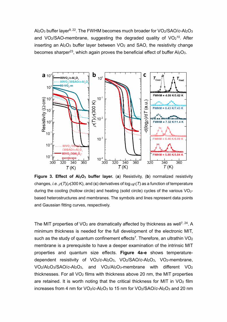
The electrical properties of the VO2 heterostructures and membranes were characterized by the temperature-dependent resistivity and corresponding derivative curves, d(logρ)/dT. Figure 3 shows that the MIT behaviour was preserved in all VO2/SAO/c-Al2O3 samples, though the steepness of resistivity change is compromised and the magnitude of the resistivity change is suppressed in contrast to the epitaxial VO2/c-Al2O3. The degraded MIT behaviour of VO2/SAO/c-Al2O3 can be mainly attributed to the defects in VO2 thin film induced by the SAO sacrificial layer. To overcome this, an Al2O3 buffer layer was inserted between VO2 thin film and SAO sacrificial layer. Figure 3a shows that the resistivity change of VO2/Al2O3/SAO/c-Al2O3 increases by around one order of magnitude and the MIT becomes much steeper. Figure 3b shows the normalized resistivity change, i.e. ρ(T)/ρ(300 K), as a function of temperature. Notably, the magnitude of the resistivity changes for VO2/SAO/c-Al2O3 and VO2-membrane are comparable, as well as for VO2/Al2O3/SAO/c-Al2O3 and VO2/Al2O3-membrane. The detailed comparison of MIT of different VO2 can be found in Table S1 in supporting information. The electrical transport measurements suggest that the influence of transferring procedure on its electrical transport properties is negligible.
To further characterize the change of MIT transition temperature (TMIT) and the sharpness of resistivity change, several parameters are defined and plotted in Figure 3c. THeat and TCool are the specific transition temperature defined as the corresponding peak position of the derivative curves, d(logρ)/dT, during heating and cooling, respectively. Hence, TMIT can be defined as TMIT = (THeat + TCool)/2. The hysteresis width (∆H) is defined as the difference between THeat and TCool. The sharpness of the transition is defined as the full width at half maximum (FWHM) of the derivative curves during heating and cooling, which is derived by Gaussian fitting. Figure 3c shows that both THeat and TCool are slightly shifted towards room temperature for VO2/SAO/c-Al2O3 and VO2/Al2O3/SAO/c-Al2O3 and their corresponding membranes by comparing with that of VO2/c-Al2O3. The decrease of TMIT indicates VO2 is compressively strained in both heterostructure and membranes forms by inserting the SAO sacrificial layer and
Al2O3 buffer layer9, 22. The FWHM becomes much broader for VO2/SAO/c-Al2O3 and VO2/SAO-membrane, suggesting the degraded quality of VO210. After inserting an Al2O3 buffer layer between VO2 and SAO, the resistivity change becomes sharper23, which again proves the beneficial effect of buffer Al2O3.
changes, i.e. ρ(T)/ρ(300 K), and (c) derivatives of log10ρ(T) as a function of temperature during the cooling (hollow circle) and heating (solid circle) cycles of the various VO2-based heterostructures and membranes. The symbols and lines represent data points and Gaussian fitting curves, respectively.
The MIT properties of VO2 are dramatically affected by thickness as well7, 24. A minimum thickness is needed for the full development of the electronic MIT, such as the study of quantum confinement effects7. Therefore, an ultrathin VO2 membrane is a prerequisite to have a deeper examination of the intrinsic MIT properties and quantum size effects. Figure 4a-e shows temperature-dependent resistivity of VO2/c-Al2O3, VO2/SAO/c-Al2O3, VO2-membrane, VO2/Al2O3/SAO/c-Al2O3, and VO2/Al2O3-membrane with different VO2 thicknesses. For all VO2 films with thickness above 20 nm, the MIT properties are retained. It is worth noting that the critical thickness for MIT in VO2 film increases from 4 nm for VO2/c-Al2O3 to 15 nm for VO2/SAO/c-Al2O3 and 20 nm
for VO2-membrane, indicating that the VO2 deteriorates when grown on SAO. Remarkably, the critical thickness recovers to 5 nm for VO2/Al2O3/SAO/c-Al2O3 and corresponding VO2/Al2O3-membrane, demonstrating that the quality of the VO2 is comparable with that of VO2 directly grown on c-Al2O3 substrate25.
Figure 4. Thickness dependent metal-insulator transition of VO2-based heterostructures and VO2-membranes. Normalized resistivity change, i.e.
ρ(T)/ρ(300 K), of (a) VO2/c-Al2O3, (b) VO2/SAO/c-Al2O3, (c) VO2-membrane, (d) VO2/Al2O3/SAO/c-Al2O3, and (e) VO2/Al2O3-membrane. The labels of the thickness in all figures correspond to the VO2 thicknesses in the respective samples.
Figure 5 compares the thickness dependence of the resistivity change across the MIT, ρ(300 K)/ρ(370 K) of different ultrathin VO2-membranes prepared in this work and the pioneer work in ref [7]. One can clearly see the magnitude of the resistivity change during the MIT in this study is over one order of magnitude better than the previous study for VO2 above 10 nm, which can still be maintained to 400% when the thickness of VO2 is reduced to 5 nm. In addition to the exceptional MIT, the water-soluable sacrificial SAO layer approach shows celebrated advantages in obtaining both large-scale, high-quality VO2
membranes with an easy-handling process.
Figure 5. Comparison of the MIT in ultrathin VO2-membranes (less than 25 nm) fabricated by different methods. The thickness dependence of the resistivity change,
ρ(300 K)/ρ(370 K), across the MIT of VO2-membranes by different fabrication methods.
Conclusion
In summary, we have demonstrated a facile synthesis method to fabricate freestanding large-scale VO2 ultrathin membranes by inserting SAO as a sacrificial layer and Al2O3 as a buffer layer between the VO2 film and c-Al2O3 substrate. Both the M-phase crystal structure and the corresponding MIT behaviour are preserved in the VO2- and VO2/Al2O3-membranes form, albeit the SAO cannot be epitaxially grown on c-Al2O3 substrate. Furthermore, the MIT quality of the VO2 membranes is notably improved by employing an Al2O3 buffer layer even for VO2 down to 5 nm, which shows great advantages as compared with the previous studies and guarantees the excellent flexibility for future low-power flexible electronics. Our VO2/Al2O3-membranes demonstrated advantages of the higher magnitude of the MIT resistivity change in a larger area and thinner VO2-membranes than the VO2-membranes prepared by other techniques. Our results could pave the way for practically and versatilely integrating high-quality MIT in future flexible electronics and photonics.
Supporting Information
Detailed comparison of MIT of different VO2 films (Table S1); Atomic force microscopy and X-ray reflectivity calibration of film thickness (Figure S1)
Acknowledgement
X.R.W. acknowledges supports from the Academic Research Fund Tier 1 (Grant No. RG177/18) from Singapore Ministry of Education, and the Singapore National Research Foundation (NRF) under the competitive Research Programs (CRP Grant No. NRF-CRP21-2018-0003), and Agency for Science, Technology and Research (A*STAR) under its AME IRG grant (Project No. A20E5c0094). D.Q. acknowledges the support of the Australian Research Council (Grant No. FT160100207) and the continued support from the Queensland University of Technology (QUT) through the Centre for Materials Science. K. H. acknowledges the support from Singapore National Research Foundation (NRF) under the Competitive Research Programs (CRP Award No. NRFCRP15-2015-01). We thank C. Yu, SW Zeng, Z. Huang, S. Goswami, A. Ariando and T. Venky Venkatasen on their fruitful discussion and help during the sample growth.
REFERENCES
(1) Imada, M.; Fujimori, A.; Tokura, Y. Metal-Insulator Transitions. Rev. Mod. Phys. 1998, 70 (4), 1039-1263. (2) Shao, Z.; Cao, X.; Luo, H.; Jin, P. Recent Progress in the Phase-Transition Mechanism and Modulation of Vanadium Dioxide Materials. NPG Asia Mater. 2018, 10 (7), 581-605. (3) Liu, K.; Lee, S.; Yang, S.; Delaire, O.; Wu, J. Recent Progresses on Physics and Applications of Vanadium Dioxide. Mater. Today 2018, 21 (8), 875-896. (4) Yi, W.; Tsang, K. K.; Lam, S. K.; Bai, X.; Crowell, J. A.; Flores, E. A. Biological Plausibility and Stochasticity in Scalable VO2 Active Memristor Neurons. Nat. Commun. 2018, 9 (1), 4661. (5) del Valle, J.; Salev, P.; Tesler, F.; Vargas, N. M.; Kalcheim, Y.; Wang, P.; Trastoy, J.; Lee, M.-H.; Kassabian, G.; Ramírez, J. G.; Rozenberg, M. J.; Schuller, I. K. Subthreshold Firing in Mott Nanodevices. Nature 2019, 569 (7756), 388-392. (6) Shukla, N.; Thathachary, A. V.; Agrawal, A.; Paik, H.; Aziz, A.; Schlom, D. G.; Gupta, S. K.; Engel-Herbert, R.; Datta, S. A Steep-Slope Transistor Based on Abrupt Electronic Phase Transition. Nat. Commun. 2015, 6 (1), 7812. (7) Fadlelmula, M. M.; Sürmeli, E. C.; Ramezani, M.; Kasırga, T. S. Effects of Thickness on the Metal–Insulator Transition in Free-Standing Vanadium Dioxide Nanocrystals. Nano Lett. 2017,
17 (3), 1762-1767. (8) Tian, Z.; Xu, B.; Hsu, B.; Stan, L.; Yang, Z.; Mei, Y. Reconfigurable Vanadium Dioxide Nanomembranes and Microtubes with Controllable Phase Transition Temperatures. Nano Lett. 2018, 18 (5), 3017-3023. (9) Sim, J. S.; Zhou, Y.; Ramanathan, S. Suspended Sub-50 nm Vanadium Dioxide Membrane Transistors: Fabrication and Ionic Liquid Gating Studies. Nanoscale 2012, 4 (22), 7056-62. (10) Pellegrino, L.; Manca, N.; Kanki, T.; Tanaka, H.; Biasotti, M.; Bellingeri, E.; Siri, A. S.; Marre, D. Multistate Memory Devices Based on Free-Standing VO2/TiO2 Microstructures Driven by Joule Self-Heating. Adv. Mater. 2012, 24 (21), 2929-34. (11) Chen, Y.; Fan, L.; Fang, Q.; Xu, W.; Chen, S.; Zan, G.; Ren, H.; Song, L.; Zou, C. Free-Standing SWNTs/VO2/Mica Hierarchical Films for High-Performance Thermochromic Devices. Nano Energy 2017, 31, 144-151. (12) Hong, S. S.; Gu, M.; Verma, M.; Harbola, V.; Wang, B. Y.; Lu, D.; Vailionis, A.; Hikita, Y.; Pentcheva, R.; Rondinelli, J. M.; Hwang, H. Y. Extreme Tensile Strain States in La0.7Ca0.3MnO3 Membranes. Science 2020, 368 (6486), 71-76. (13) Peter, A. P.; Martens, K.; Rampelberg, G.; Toeller, M.; Ablett, J. M.; Meersschaut, J.; Cuypers, D.; Franquet, A.; Detavernier, C.; Rueff, J.-P.; Schaekers, M.; Van Elshocht, S.; Jurczak, M.; Adelmann, C.; Radu, I. P. Metal-Insulator Transition in ALD VO2 ultrathin Films and Nanoparticles: Morphological Control. Adv. Funct. Mater. 2015, 25 (5), 679-686. (14) Hong, S. S.; Yu, J. H.; Lu, D.; Marshall, A. F.; Hikita, Y.; Cui, Y.; Hwang, H. Y. Two-Dimensional Limit of Crystalline Order in Perovskite Membrane Films. Sci. Adv. 2017, 3 (11), eaao5173. (15) Lu, D.; Baek, D. J.; Hong, S. S.; Kourkoutis, L. F.; Hikita, Y.; Hwang, Harold Y. Synthesis of Freestanding Single-Crystal Perovskite Films and Heterostructures by Etching of Sacrificial Water-Soluble layers. Nat. Mater. 2016, 15 (12), 1255-1260. (16) Dong, G.; Li, S.; Yao, M.; Zhou, Z.; Zhang, Y. Q.; Han, X.; Luo, Z.; Yao, J.; Peng, B.; Hu, Z.; Huang, H.; Jia, T.; Li, J.; Ren, W.; Ye, Z. G.; Ding, X.; Sun, J.; Nan, C. W.; Chen, L. Q.; Li, J.; Liu, M. Super-Elastic Ferroelectric Single-Crystal Membrane with Continuous Electric Dipole Rotation. Science 2019, 366 (6464), 475-479. (17) Ji, D.; Cai, S.; Paudel, T. R.; Sun, H.; Zhang, C.; Han, L.; Wei, Y.; Zang, Y.; Gu, M.; Zhang, Y.; Gao, W.; Huyan, H.; Guo, W.; Wu, D.; Gu, Z.; Tsymbal, E. Y.; Wang, P.; Nie, Y.; Pan, X. Freestanding Crystalline Oxide Perovskites Down to the Monolayer Limit. Nature 2019, 570 (7759), 87-90. (18) Han, K.; Hu, K.; Li, X.; Huang, K.; Huang, Z.; Zeng, S.; Qi, D.; Ye, C.; Yang, J.; Xu, H.; Ariando, A.; Yi, J.; Lu, W.; Yan, S.; Wang, X. R. Erasable and Recreatable Two-Dimensional Electron Gas at the Heterointerface of SrTiO3 and a Water-Dissolvable Overlayer. Sci. Adv. 2019, 5 (8), eaaw7286. (19) Chen, F. H.; Fan, L. L.; Chen, S.; Liao, G. M.; Chen, Y. L.; Wu, P.; Song, L.; Zou, C. W.; Wu, Z. Y. Control of the Metal-Insulator Transition in VO2 Epitaxial Film by Modifying Carrier Density. ACS Appl. Mater. Interfaces 2015, 7 (12), 6875-81. (20) Hada, M.; Okimura, K.; Matsuo, J. Characterization of Structural Dynamics of VO2 Thin Film on c-Al2O3 Using in-Air Time-Resolved X-Ray Diffraction. Phys. Rev. B 2010, 82 (15), 153401. (21) Yang, M.; Yang, Y.; Wang, L.; Hong, B.; Huang, H.; Hu, X.; Zhao, Y.; Dong, Y.; Li, X.; Lu,
Y.; Bao, J.; Luo, Z.; Gao, C. For Progress in Natural Science: Materials International Investigations of Structural Phase Transformation and THz Properties across Metal–Insulator Transition in VO2/ Al2O3 Epitaxial Films. Prog. Nat. Sci-Mater 2015, 25 (5), 386-391. (22) Muraoka, Y.; Hiroi, Z. Metal–Insulator Transition of VO2 Thin Films Grown on TiO2 (001) and (110) Substrates. Appl. Phys. Lett. 2002, 80 (4), 583-585. (23) Lee, D.; Lee, J.; Song, K.; Xue, F.; Choi, S. Y.; Ma, Y.; Podkaminer, J.; Liu, D.; Liu, S. C.; Chung, B.; Fan, W.; Cho, S. J.; Zhou, W.; Lee, J.; Chen, L. Q.; Oh, S. H.; Ma, Z.; Eom, C. B. Sharpened VO2 Phase Transition Via Controlled Release of Epitaxial Strain. Nano Lett 2017, 17 (9), 5614-5619. (24) Yamin, T.; Wissberg, S.; Cohen, H.; Cohen-Taguri, G.; Sharoni, A. Ultrathin Films of VO2 on r-Cut Sapphire Achieved by Postdeposition Etching. ACS Appl. Mater. Interfaces 2016, 8 (23), 14863-70. (25) Zhang, H.-T.; Zhang, L.; Mukherjee, D.; Zheng, Y.-X.; Haislmaier, R. C.; Alem, N.; Engel-Herbert, R. Wafer-Scale Growth of VO2 Thin Films Using a Combinatorial Approach. Nat. Commun. 2015, 6 (1), 8475.
S-1
Supporting Information
Enhanced metal-insulator transition in freestanding VO2 down to 5 nm thickness
Kun Han1,2, †, Liang Wu1,3, † *, Yu Cao4, †, Hanyu Wang5, Chen Ye1, Ke Huang1, M. Motapothula6,7, Hongna Xing8, Xinghua Li8, Dong-Chen Qi9, Xiao Li5, X. Renshaw Wang1,10,* 1Division of Physics and Applied Physics, School of Physical and Mathematical Sciences, Nanyang Technological University, 21 Nanyang Link,637371, Singapore
2Key Laboratory of Structure and Functional Regulation of Hybrid Materials of Ministry of Education, Institutes of Physical Science and Information Technology, Anhui University, Hefei 230601, China
3School of Material Science and Engineering, Kunming University of Science and Technology, Kunming, Yunnan 650093, China
4Department of Electrical and Computer Engineering, National University of Singapore, 4 Engineering Drive 3, Singapore 117583
5NNU-SULI Thermal Energy Research Center, Center for Quantum Transport and Thermal Energy Science (CQTES), School of Physics and Technology, Nanjing Normal University, Nanjing 210023, China
6Department of Physics and Astronomy, Uppsala University, Box 516, SE-75120 Uppsala, Sweden
7Department of Physics, SRM University AP, Amaravati, Andhra Pradesh 522-502, India
8School of Physics, Northwest University, Xi’an 710069, China
9Centre for Materials Science, School of Chemistry and Physics, Queensland University of Technology, Brisbane, QLD 4001, Australia
10School of Electrical and Electronic Engineering, Nanyang Technological University, 50 Nanyang Ave, 639798, Singapore
To quantitatively evaluate the quality of our VO2 films and membranes, several key parameters are defined and listed in Table S1.
S-3
Figure S1
The thickness of VO2 films is calibrated by results of profilometry (Figure S1a,b) and X-ray reflectivity (Figure S1c). Both results are consistent, which provides the thickness controlling by counting the number of the laser pulse. For VO2, 1 nm corresponds to 500 pulses; For Al2O3, 1 nm corresponds to 20 pulses.
Supplementary Figure S1. Thickness calibration of different VO2. The thicknesses of (a) 40000 pulses VO2-membrane and (b) 40000 pulses VO2/600 pulses Al2O3 were measured by Bruker profilometer. (c) The X-ray reflectivity (XRR) of 30000 pulses VO2/c-Al2O3 heterostructure. The thickness of the VO2 film obtained by fitting is 58.8 nm. The thicknesses measured by both methods are consistent. All the thicknesses used in this study are calibrated by the laser pulses.