Enhanced Ultra-Wideband (UWB) Circular Monopole Antenna with Electromagnetic Band Gap (EBG) Surface and Director by Amir I Zaghloul, Youn M Lee, Gregory A Mitchell, and Theodore K Anthony ARL-TR-7041 August 2014 Approved for public release; distribution unlimited.
Transcript
Enhanced Ultra-Wideband (UWB) Circular Monopole
Antenna with Electromagnetic Band Gap (EBG) Surface
and Director
by Amir I Zaghloul, Youn M Lee, Gregory A Mitchell, and
Theodore K Anthony
ARL-TR-7041 August 2014
Approved for public release; distribution unlimited.
NOTICES
Disclaimers
The findings in this report are not to be construed as an official Department of the Army position
unless so designated by other authorized documents.
Citation of manufacturer’s or trade names does not constitute an official endorsement or
approval of the use thereof.
Destroy this report when it is no longer needed. Do not return it to the originator.
Army Research Laboratory Adelphi, MD 20783-1138
ARL-TR-7041 August 2014
Enhanced Ultra-Wideband (UWB) Circular Monopole
Antenna with Electromagnetic Band Gap (EBG) Surface
and Director
Amir I Zaghloul, Youn M Lee, Gregory A Mitchell, and
Theodore K Anthony Sensors and Electron Devices Directorate, ARL
Approved for public release; distribution unlimited.
ii
REPORT DOCUMENTATION PAGE Form Approved
OMB No. 0704-0188 Public reporting burden for this collection of information is estimated to average 1 hour per response, including the time for reviewing instructions, searching existing data sources, gathering and maintaining the
data needed, and completing and reviewing the collection information. Send comments regarding this burden estimate or any other aspect of this collection of information, including suggestions for reducing the
burden, to Department of Defense, Washington Headquarters Services, Directorate for Information Operations and Reports (0704-0188), 1215 Jefferson Davis Highway, Suite 1204, Arlington, VA 22202-4302.
Respondents should be aware that notwithstanding any other provision of law, no person shall be subject to any penalty for failing to comply with a collection of information if it does not display a currently
valid OMB control number.
PLEASE DO NOT RETURN YOUR FORM TO THE ABOVE ADDRESS.
1. REPORT DATE (DD-MM-YYYY)
August 2014
2. REPORT TYPE
Final
3. DATES COVERED (From - To)
4. TITLE AND SUBTITLE
Enhanced Ultra-Wideband (UWB) Circular Monopole Antenna with
Electromagnetic Band Gap (EBG) Surface and Director
5a. CONTRACT NUMBER
5b. GRANT NUMBER
5c. PROGRAM ELEMENT NUMBER
6. AUTHOR(S)
Amir I Zaghloul, Youn M Lee, Gregory A Mitchell, and Theodore K Anthony
5d. PROJECT NUMBER
5e. TASK NUMBER
5f. WORK UNIT NUMBER
7. PERFORMING ORGANIZATION NAME(S) AND ADDRESS(ES)
U.S. Army Research Laboratory
ATTN: RDRL-SER-M
2800 Powder Mill Road
Adelphi, MD 20783-1138
8. PERFORMING ORGANIZATION REPORT NUMBER
ARL-TR-7041
9. SPONSORING/MONITORING AGENCY NAME(S) AND ADDRESS(ES)
10. SPONSOR/MONITOR'S ACRONYM(S)
11. SPONSOR/MONITOR'S REPORT NUMBER(S)
12. DISTRIBUTION/AVAILABILITY STATEMENT
Approved for public release; distribution unlimited.
13. SUPPLEMENTARY NOTES
14. ABSTRACT
A circular monopole antenna fed with a coplanar waveguide is designed as an ultra-wideband (UWB) antenna for ground-
penetrating radar. The performance of the antenna is enhanced by adding an electromagnetic band gap (EBG) surface on one
side and a monopole director on the other side. The EBG surface can be a single-resonance structure or dual or multi-
resonance structure for wider bandwidth. The enhanced design shows higher and flatter gain across the wideband, with
different levels of improvements, depending on the choice of the additional layers, which also impacts the overall profile of
the antenna. Simulation results of a number of designs are presented, along with measurement results of one design.
Comparison of measured and simulated results is presented and shows good agreement. The target frequency band for the
4. Electromagnetic Band Gap Surface (EBG) Design 5
5. Director Design 9
6. UWB Antenna with EBG and Director 11
7. Prototype Fabrication and Measurements 12
8. Simulation of Ground Penetration of Radio Frequency (RF) Signals 16
9. Conclusions 19
10. References 20
Distribution List 21
iv
List of Figures
Fig. 1 Layout and picture of the basic UWB circular monopole antenna ......................................2
Fig. 2 Computed S11 of the basic UWB circular monopole antenna ............................................2
Fig. 3 Computed 3-D radiation pattern of the UWB monopole antenna at 0.9 GHz .....................3
Fig. 4 Computed realized gain of the antenna at broadside from 0.7–3.0 GHz.............................3
Fig. 5 A typical 3-element Yagi-Uda dipole array ........................................................................4
Fig. 6 The concept of enhanced UWB monopole antenna ............................................................5
Fig. 7 Conventional mushroom EBG surface (left) vs. EBG surface without vias/pins (right) ....5
Fig. 8 Antenna gain comparison computed from 0.7–3 GHz for UWB circular monopole antenna in free space (red squares) and the antenna over a single-layer mushroom EBG (blue diamonds) .........................................................................................................................6
Fig. 9 Layout of a section of a 2-layer EBG structure above a ground plane ...............................7
Fig. 10 Model of the circular monopole antenna above the ground plane and two EBG layers and fiberglass support structure; only half of the total structure is shown ....................8
Fig. 11 Computed realized gain of the UWB antenna with 2-layer EBG without pins at broadside (blue) is overlaid with that of the antenna with no EBG layers (red) .......................8
Fig. 12 Computed 3-D views of the radiation patterns at 0.7, 1.2, 1.4, and 2.7 GHz. The radiation pattern is plotted over the antenna structure at 700 MHz to show the orientation of the antenna relative to the radiation pattern. ..........................................................................9
Fig. 13 The plot is for S11 of an antenna with a director. Beyond the third marker is –10 dB in return loss, starting at 1.2 GHz. ...........................................................................................10
Fig. 14 Antenna return loss computed from 0.7–3 GHz. The blue line with diamond tick marks is the realized gain of the antenna. Antenna with a director was also computed and their combined result is plotted in red with square tick marks. ...............................................10
Fig. 15 Return loss plot of an UWB antenna with a director and the EBG structure ..................11
Fig. 16 Realized gain plot of an UWB antenna with different combinations of adding a single-layer EBG reflective surface and a director ..................................................................12
Fig. 17 A picture of the fabricated UWB antenna over a 2-layer EBG surface without pins .....12
Fig. 18 Measured S11 (black) of the EBG antenna overlaid with computed S11 (red) ..............13
Fig. 19 Realized gain for UWB antenna: Red, simulated UWB circular dipole; Blue, simulated UWB antenna over 2-layer EBG surface; and Black: measured fabricated UWB antenna over 2-layer EBG ............................................................................................14
Fig. 20 Comparison of E-plane cut of the normalized E-field radiation patterns at 1.0, 1.4, 2.2, and 2.7 GHz. The red curve represents the computed data and the black represents the measured data for the UWB antenna over the 2-layer EBG surface. ................................15
v
Fig. 21 Comparison of H-plane cut of the normalized E-field radiation patterns at 1.0, 1.4, 2.2, and 2.7 GHz. The red curve represents the computed data and the black represents the measured data for the UWB antenna over the 2-layer EBG surface. ................................16
Fig. 22 Contour plot of the E-plane cut for the E-field at 0.9 GHz as it penetrates the ground ..17
Fig. 23 Contour plot of the H-plane cut for the E-field at 0.9 GHz as it penetrates the ground ..17
Fig. 24 Contour plot of the E-plane cut for the E-field at 1.4 GHz as it penetrates the ground ..18
Fig. 25 Contour plot of the H-plane cut for the E-field at 1.4 GHz as it penetrates the ground and bulk conductivity is 0.005 S/m. Because of a symmetry used in computation, only left half of the geometry and contour plot are shown. .....................................................18
vi
INTENTIONALLY LEFT BLANK.
1
1. Introduction
This report describes the design, fabrication, and testing of a prototype antenna for an application
in ground-penetrating radar (GPR). The application of this antenna is for the detection of buried
objects by Soldiers on foot using a handheld device.
The design goals for the antenna were to obtain return loss (S11) less than –10 dB with a positive
realized gain for a frequency range of 0.7–3 GHz. Furthermore, the size of the antenna is not to
exceed 15.24 x 15.24 x 7.62 cm (6 x 6 x 3 inches) as a design goal. Since the antenna structure is
handheld, the weight of the antenna is a critical design component. Therefore, an effort is made
to incorporate lightweight materials in the antenna design to minimize the total weight while
meeting the above criteria.
If the signal transmitted and received by the antenna is in the form of a narrow pulse, an ultra-
wideband (UWB) antenna would be needed. To reconstruct the pulse with high fidelity, the
antenna gain should have minimum variation over the frequency band. The minimum gain
variation over the band may also be desirable in stepped continuous wave (CW) GPR systems.
Although the system may have the ability to calibrate out the gain variation with frequency,
adding the gain variation as a parameter was considered a factor in choosing the multi-layer
structure presented in this report.
The design philosophy evolved as follows. The basic UWB monopole antenna radiates on both
sides of the flat circular radiator with a wide gain variation over the required bandwidth of
0.7–3.0 GHz. GPR systems require the antenna to radiate in one direction, with a high front-to-
back ratio in the radiation pattern. Conventional GPR antenna designs use cavity-backed spiral
antennas with the right depth for the cavity or an absorber-backed cavity. This results in a limited
bandwidth that depends on the cavity dimensions or lower gain as a result of the energy
dissipation in the absorber.
2. UWB Circular Monopole Antenna
A well-known circular monopole UWB antenna fed by a coplanar waveguide1 was chosen as a
candidate antenna because of past experiences in working with this type of antenna design. The
antenna was simulated and various parameters such as coplanar waveguide dimensions and
radius of the antenna were optimized using High Frequency Structural Simulator (HFSS)
software. The substrate of the antenna is a 0.1524 cm-(0.06 inch)-thick, Rogers 4350b dielectric
material. This substrate was chosen to limit the size of the antenna to be within the size and
2
weight design constraints. The relative dielectric constant (εr) of the substrate is 3.48. Figure 1
shows the layout of the basic UWB circular monopole antenna fed by a coplanar waveguide.
Fig. 1 Layout and picture of the basic UWB circular monopole antenna
The design of the antenna structure was optimized by iterations using HFSS. The radius of the
circular monopole was chosen to fit the given size limit of the substrate based on this
optimization. The antenna feed incorporates a coplanar waveguide to maximize its performance
and attain the best match in the lower part of the frequency band. Figure 2 shows the S11 of the
antenna shown in Fig. 1. It shows good return loss across the design frequency band.
Fig. 2 Computed S11 of the basic UWB circular monopole antenna
Figure 3 shows a computed three-dimensional (3-D) radiation pattern of the antenna at 0.9 GHz.
As noted in Fig. 1, the antenna is placed on the x-y plane, and the SMA connector feeding the
antenna is located at coordinates’ origin such that the monopole is along the y-axis. The pattern
is expected to be nearly uniform in the perpendicular x-z plane and directional in the y-z plane, as
verified in the simulated pattern in Fig. 3. The realized gain of the monopole is shown in Fig. 4,
which varies by more than 17 dB over the frequency band of interest. Clearly seen in Fig. 4 is the
fact that the realized gain only stays positive from 0.7–1.6 GHz. The uniform radiation in all
directions in the x-z plane is not needed for the GPR application, where only half-space radiation
is required. Limiting the beam to half-space radiation would increase the gain, which is the main
purpose of modifying the circular monopole design by adding other layers. Also, the 17-dB
-60
-40
-20
0
0.5 1 1.5 2 2.5 3
Ret
urn
loss
, dB
Frequency, GHz
3
variation of the gain over the frequency band may introduce errors in reconstructing the pulsed
signal that occupies the full 0.7–3.0 GHz band.
Fig. 3 Computed 3-D radiation pattern of the UWB
monopole antenna at 0.9 GHz
Fig. 4 Computed realized gain of the antenna at broadside from 0.7–3.0 GHz
3. Design Enhancement Using Yagi-Uda Concept
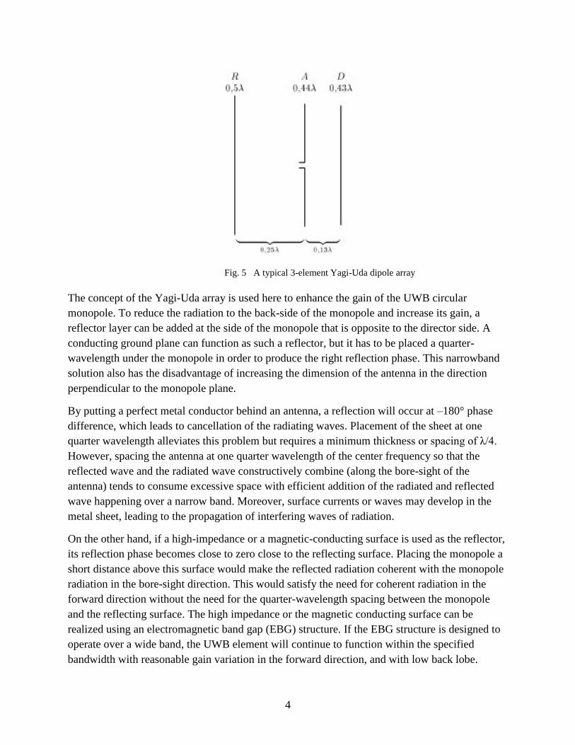
The Yagi-Uda dipole array2,3
is a directional antenna consisting of a driven element (usually a
dipole or folded dipole) and additional parasitic elements (referred to as a reflector and one or
more directors). Figure 5 shows a typical 3-element Yagi-Uda array. The induced currents on the
reflector and director dipoles have a phase relative to the driven dipole that is a function of the
spacing, and such that their radiation in the forward direction is coherent with that of that driven
dipole. On the other hand, the radiations in the backward direction cancel each other, and the
array radiation pattern forms a directive beam with a high front to back ratio. The result is a
higher gain antenna relative to the dipole’s omnidirectional gain.
-20
-15
-10
-5
0
5
0.5 1 1.5 2 2.5 3
dB
i
Frequency, GHz
4
Fig. 5 A typical 3-element Yagi-Uda dipole array
The concept of the Yagi-Uda array is used here to enhance the gain of the UWB circular
monopole. To reduce the radiation to the back-side of the monopole and increase its gain, a
reflector layer can be added at the side of the monopole that is opposite to the director side. A
conducting ground plane can function as such a reflector, but it has to be placed a quarter-
wavelength under the monopole in order to produce the right reflection phase. This narrowband
solution also has the disadvantage of increasing the dimension of the antenna in the direction
perpendicular to the monopole plane.
By putting a perfect metal conductor behind an antenna, a reflection will occur at –180° phase
difference, which leads to cancellation of the radiating waves. Placement of the sheet at one
quarter wavelength alleviates this problem but requires a minimum thickness or spacing of λ/4.
However, spacing the antenna at one quarter wavelength of the center frequency so that the
reflected wave and the radiated wave constructively combine (along the bore-sight of the
antenna) tends to consume excessive space with efficient addition of the radiated and reflected
wave happening over a narrow band. Moreover, surface currents or waves may develop in the
metal sheet, leading to the propagation of interfering waves of radiation.
On the other hand, if a high-impedance or a magnetic-conducting surface is used as the reflector,
its reflection phase becomes close to zero close to the reflecting surface. Placing the monopole a
short distance above this surface would make the reflected radiation coherent with the monopole
radiation in the bore-sight direction. This would satisfy the need for coherent radiation in the
forward direction without the need for the quarter-wavelength spacing between the monopole
and the reflecting surface. The high impedance or the magnetic conducting surface can be
realized using an electromagnetic band gap (EBG) structure. If the EBG structure is designed to
operate over a wide band, the UWB element will continue to function within the specified
bandwidth with reasonable gain variation in the forward direction, and with low back lobe.
5
Following the Yagi-Uda design, an undriven director is located on the other side of the active
monopole and uses the same design with smaller dimensions. The resultant combination
EBG/UWB monopole radiator/monopole director element (Fig. 6) produces the desired function
based on using the Yagi-Uda array concept.4,5
Fig. 6 The concept of enhanced UWB monopole antenna
4. Electromagnetic Band Gap Surface (EBG) Design
EBG surfaces act as perfect magnetic conductors (PMCs) at a resonance frequency determined
by the dimensions of the surface components. In contrast with the perfect electric conductor
(PEC), which has a reflection phase of 180°, the PMC has a reflection phase of 0° at resonance.
This enhances the radiation of an antenna placed on this surface by reflecting an in-phase, or
coherent, signal that adds to the antenna radiation. One of the common EBG designs, known as
mushroom design, is based on a periodic array of patches connected to a ground plane via
conductive pins, as shown in Fig. 7. A variation on that design removes the pins with proper
adjustments in the patch and array dimensions, are also shown in Fig. 7. The removal of the pins
simplifies the fabrication of the EBG surface.
Fig. 7 Conventional mushroom EBG surface (left) vs. EBG surface without vias/pins (right)
6
Conventional EBGs have narrow bandwidths that are considered ineffective in wideband cases
such as the UWB antenna discussed in this report. An example of results using a conventional
single-layer mushroom (patches with pins) EBG as the reflector surface is shown in Fig. 8. It
shows improvement over the UWB monopole without EBG, but still shows negative gain in part
of the band.
Fig. 8 Antenna gain comparison computed from 0.7–3 GHz for UWB circular monopole antenna in
free space (red squares) and the antenna over a single-layer mushroom EBG (blue diamonds)
Two methods to increase the EBG surface bandwidth are to use progressive6,7
or stacked EBG8,9
structures that produce the required high-impedance surface over a broad band. The stacked EBG
is chosen for the current UWB monopole. The design is made of multiple layers of periodic
patches, as shown in Fig. 9. Because of the difficulty in fabricating stacked mushroom EBG
layers, it was chosen to use layers of different patch sizes without pins or vias. The figure shows
a section of a 2-layer EBG structure that would be placed closely under the UWB monopole. The
height of the monopole above the EBG surface can be considerably less than the λ/4 required
above a PEC surface. The dimensions of the periodic patches at the two layers are chosen to
produce two resonances within the wide band of the antenna, with the net effect of broadband of
reflection phase within a ±90° phase.
-15
-10
-5
0
5
10
0 0.5 1 1.5 2 2.5 3 3.5
7
Fig. 9 Layout of a section of a 2-layer EBG structure
above a ground plane
For the UWB antenna, operating over the 0.7–3.0 GHz band, the EBG layers are made of small
patches of thin copper sheet bonded to the top or bottom of a dielectric substrate in a periodic
fashion. The dimensions of the bottom EBG layer are 34 x 37 mm (1.34 x 1.46 inches), and the
dimensions of the top EBG layer are 17 x 18.5 mm (0.669 x 0.728 inches). The bottom layer
faces the ground plane and the top layer faces the antenna aperture. These orientations were
chosen to optimize the results of gain calculations in HFSS. There is an air gap of 0.8 mm
(0.031 inches) that exists between the copper patches comprising both EBG layers. There is a
22.35 mm (0.88 inch) thick sheet of foam placed between the two EBG layers, and a 25.4 mm
(1 inch) thick sheet of foam between the second EBG layer and the ground plane. This was done
to provide a flat surface for the EBG layers without affecting the electromagnetic performance of
the antenna since foam is very nearly equivalent to air in terms of its electromagnetic properties.
Figure 10 shows the final design of the antenna including the ground plane and EBG layers of
Fig. 9 as well as the antenna aperture of Fig. 1. It should be noted that the depiction of the
antenna in Fig. 10 is mirrored about the y-axis. The support structure of the antenna (shown in
green) is made of narrow FR4 fiberglass strips and is held together by an epoxy adhesive. The
thickness of the fiberglass varies from 1.59–3.18 mm (0.0625–0.125 inches).
8
Fig. 10 Model of the circular monopole antenna
above the ground plane and two EBG layers
and fiberglass support structure; only half
of the total structure is shown
The antenna design of Fig. 10 was simulated using HFSS and its performance was compared
with the basic UWB antenna, shown in Fig. 1, and its gain and radiation pattern performances,
shown in Figs. 11 and 12. The effect of adding the EBG layers is demonstrated in Fig. 11, where
the gain at broadside exhibits significant increase relative to the UWB antenna by itself, as much
as 18 dB at one point in the frequency response. In addition, the gain variation over the
frequency band of interest (0.7–3.0 GHz) is reduced to around 8 dB, versus the 17 dB gain
variation for the basic UWB antenna.
Fig. 11 Computed realized gain of the UWB antenna with 2-layer EBG without pins
at broadside (blue) is overlaid with that of the antenna with no EBG layers (red)
-16
-12
-8
-4
0
4
8
0.5 1 1.5 2 2.5 3
9
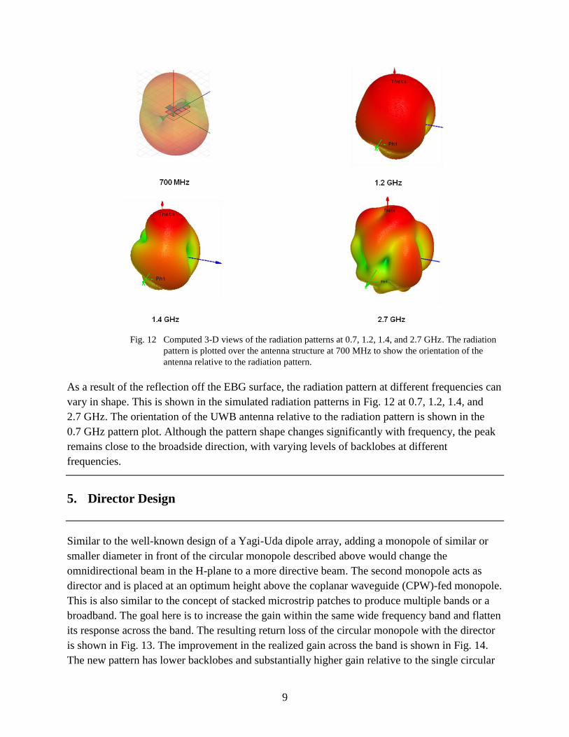
Fig. 12 Computed 3-D views of the radiation patterns at 0.7, 1.2, 1.4, and 2.7 GHz. The radiation
pattern is plotted over the antenna structure at 700 MHz to show the orientation of the
antenna relative to the radiation pattern.
As a result of the reflection off the EBG surface, the radiation pattern at different frequencies can
vary in shape. This is shown in the simulated radiation patterns in Fig. 12 at 0.7, 1.2, 1.4, and
2.7 GHz. The orientation of the UWB antenna relative to the radiation pattern is shown in the
0.7 GHz pattern plot. Although the pattern shape changes significantly with frequency, the peak
remains close to the broadside direction, with varying levels of backlobes at different
frequencies.
5. Director Design
Similar to the well-known design of a Yagi-Uda dipole array, adding a monopole of similar or
smaller diameter in front of the circular monopole described above would change the
omnidirectional beam in the H-plane to a more directive beam. The second monopole acts as
director and is placed at an optimum height above the coplanar waveguide (CPW)-fed monopole.
This is also similar to the concept of stacked microstrip patches to produce multiple bands or a
broadband. The goal here is to increase the gain within the same wide frequency band and flatten
its response across the band. The resulting return loss of the circular monopole with the director
is shown in Fig. 13. The improvement in the realized gain across the band is shown in Fig. 14.
The new pattern has lower backlobes and substantially higher gain relative to the single circular
10
monopole. The gain of the circular monopole is identified in Fig. 14 by blue diamond-shaped
plot. The gain of the monopole with a director is identified by the red square-shaped plot. It
should be noted that the improvement in the return loss in the middle portion of the band
corresponds to the higher realized gain, which also extends beyond the center portion.
Fig. 13 The plot is for S11 of an antenna with a director. Beyond the third marker is –10 dB in return loss,
starting at 1.2 GHz.
Fig. 14 Antenna return loss computed from 0.7–3 GHz. The blue line with diamond tick marks is the
realized gain of the antenna. Antenna with a director was also computed and their combined result is
plotted in red with square tick marks.
11
6. UWB Antenna with EBG and Director
Following the analogy of the Yagi-Uda array, to reduce the radiation to the back side of the
monopole and increase its gain, a reflector layer can be added at the side of the monopole that is
opposite to the director side. A conducting ground plane can function as such a reflector, but it
has to be placed a quarter-wavelength under the monopole in order to produce the right reflection
phase. This narrowband solution also has the disadvantage of increasing the dimension of the
antenna in the direction perpendicular to the monopole plane. An alternative to the conducting-
plane reflector is the EBG surface. The EBG surface can be designed to operate over a wide
band, and because of its reflection phase characteristics, it can be placed close to the monopole
plane. This reduces the overall size of the antenna.
An example of such design of the UWB antenna with a director and a single-layer mushroom
EBG surface was simulated to show the concept. The return loss plot of the monopole-plus-
director over an EBG surface is shown in Fig. 15.
Fig. 15 Return loss plot of an UWB antenna with a director and the EBG structure
The effect of adding the EBG surface on the gain of the director-enhanced monopole antenna is
shown in Fig. 16. The figure shows the four cases of the circular monopole by itself, the circular
monopole with a director, the circular monopole over a single-layer EBG reflector surface with
pins, and the circular monopole with a director on one side over a reflective single-layer EBG
surface with pins on the other side. The figure shows that the combination of a director element
in front of the monopole and an EBG reflector surface behind it produce the predicted Yagi-Uda
effect of high directive gain across the wide frequency band.
12
Fig. 16 Realized gain plot of an UWB antenna with different combinations of adding a single-layer EBG
reflective surface and a director
7. Prototype Fabrication and Measurements
A prototype for the UWB antenna was fabricated and tested. The design selected for fabrication
is the UWB with two layers of EBG surfaces with no pins, as shown in Fig. 10. A picture of the
fabricated antenna is shown in Fig. 17. To limit the height of the element and keep it within the
design goal of 3 inches, no director element was added. The simulated realized gain was shown
previously in Fig. 11. That figure shows realized gain of the antenna at broadside from 0.7 to
3.0 GHz. The realized gain (blue) improves considerably over that of the UWB element by itself.
The addition of the two EBG layers has resulted in an improvement of nearly 17 dB over this
range.
Fig. 17 A picture of the fabricated UWB antenna over a 2-layer
EBG surface without pins
To measure the prototype antenna in the anechoic chamber, an end launcher was used to excite
the antenna structure. This end launcher has two sets of tabs designed to secure it against the
A Picture of
Fabricated Antenna
13
substrate. However, the presence of these tabs caused noticeable effects on the measured return
loss versus simulation especially above 2.3 GHz. To remedy this, the tabs were removed and thin
strips of fiberglass were added on either side of the end launcher using epoxy adhesive to bond
the connector to the fiberglass strips.
Figure 18 shows the measured S11 in black overlaid with that of the computed values in red. The
S11 of the antenna in Fig. 17 shows some deterioration compared to that of the original antenna
in Fig. 2 because of the presence of the EBG layers and fiberglass frame. This deterioration
causes our antenna to have a worse S11 than the design goal of –10 dB over the frequency range.
The measured gain of the antenna is plotted in Fig. 19 and compared with the simulated realized
gain of original UWB monopole and the simulated gain of the UWB antenna over the 2-layer
EBG. Both measured and simulated results for the EBG-backed UWB antenna show
improvement over the original design. However, discrepancies between simulated and measured
results indicate fabrication issues and possible bandwidth limitations in the fabricated EBG
relative to the simulation. Further studies in the design are warranted.
Freq [GHz]
0.5 0.8 1.0 1.3 1.5 1.8 2.0 2.3 2.5 2.8 3.0
Ret
urn
lo
ss,
dB
-40
-35
-30
-25
-20
-15
-10
-5
0
Fig. 18 Measured S11 (black) of the EBG antenna overlaid with computed S11 (red)
14
Fig. 19 Realized gain for UWB antenna: Red, simulated UWB circular dipole; Blue, simulated UWB
antenna over 2-layer EBG surface; and Black: measured fabricated UWB antenna over
2-layer EBG
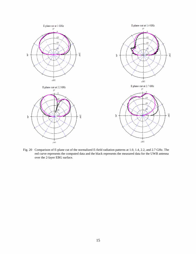
The radiation patterns were measured and compared with the simulation. Figure 20 shows the
radiation patterns of the E-plane cut at 1.0, 1.4, 2.2, and 2.7 GHz. The red curves represent
simulated patterns and the black curves represent the measured patterns. Figure 21 shows the
radiation patterns of H-plane cut at 1.0, 1.4, 2.2, and 2.7 GHz. Again, the red curves represent
simulated patterns and the black curves represent the measured patterns. Figures 20 and 21 show
agreement between the simulated and measured patterns.
Since the antenna will be used for GPR, the radiation patterns are only measured for the top
hemisphere. The radiation patterns shown in Figs. 20 and 21 are normalized for easy
comparison. There are some minor discrepancies, but generally there is good agreement between
simulation and measurement. The weight of the final prototype was measured to be 299.4 gm
(0.66 lb).
15
Fig. 20 Comparison of E-plane cut of the normalized E-field radiation patterns at 1.0, 1.4, 2.2, and 2.7 GHz. The
red curve represents the computed data and the black represents the measured data for the UWB antenna
over the 2-layer EBG surface.
16
Fig. 21 Comparison of H-plane cut of the normalized E-field radiation patterns at 1.0, 1.4, 2.2, and 2.7 GHz. The
red curve represents the computed data and the black represents the measured data for the UWB antenna
over the 2-layer EBG surface.
8. Simulation of Ground Penetration of Radio Frequency (RF) Signals
To understand how the antenna will interact with the ground, the antenna structure was simulated
as placed 76.2 mm (3 inches) above a ground plane and was excited with a 1-V/m signal source
using HFSS. The simulated ground extended five wavelengths in all directions from the antenna.
These wavelengths correspond to 0.7 GHz. The ground has an εr = 8 and the bulk conductivity
was 0.005 S/m.
Figure 22 shows a contour plot of the E-plane cut for the E-field at 0.9 GHz. The magnitude
varies from approximately 1–4
to 100 V/m. Figure 23 shows a contour plot of the H-plane cut for
the E-field at 0.9 GHz. Again, the magnitude varies from approximately 1–4
to 100 V/m. It
should be noted the field distribution in Fig. 23 is mirrored about the vertical axis.
17
Fig. 22 Contour plot of the E-plane cut for the E-field at 0.9 GHz as it penetrates the ground
Fig. 23 Contour plot of the H-plane cut for the E-field at 0.9 GHz as it penetrates the ground
Figure 24 shows a contour plot of the E-plane cut for the E-field, while Fig. 25 shows a contour
plot of the H-plane cut for the E-field, both at 1.4 GHz. It should be noted the field distribution in
Fig. 25 is mirrored about the vertical axis.
18
Fig. 24 Contour plot of the E-plane cut for the E-field at 1.4 GHz as it penetrates the ground
Fig. 25 Contour plot of the H-plane cut for the E-field at 1.4 GHz as it penetrates
the ground and bulk conductivity is 0.005 S/m. Because of a symmetry used in
computation, only left half of the geometry and contour plot are shown.
19
9. Conclusions
Adding two EBG layers to the original circular monopole antenna aperture improved the realized
gain of the UWB antenna by up to 17 dB across the frequency band of interest. A positive
realized gain was achieved across most of the frequency band at the expense of a return loss of
worse than –10 dB over large parts of the band. Simulations of E- and H-plane radiation patterns
were compared to measurement and show good agreement for most of the frequencies analyzed.
Discrepancies between simulated and measured gain of the 2-layer EBG-backed UWB antenna
existed and are due to fabrication tolerances and bandwidth limitations that can be eliminated by
more optimization of the dimensions of the EBG structure. Further optimizations and studies of
the stacked EBG are continuing beyond the scope of this report.
Contour plots of the E-field penetrating the ground were also simulated to show the signal
behavior of the ground penetration for this antenna design. The dimensions of the antenna met
the size and weight constraints of the design while achieving good realized gain and ground
penetration performance.
20
10. References
1. Allen B, Dohler M, Okon EE, Malik WQ, Brown AK, Edwards DJ. Ultra-wideband antennas
and propagation for communications, radar, and imaging. West Sussex (England): John
Wiley & Sons, Ltd.; 2007.
2. Thiele GA. Analysis of Yagi-Uda-type antennas. IEEE Transactions on Antennas and
Propagation. January 1969;AP-17(1):24–31.
3. Bojsen JH, Schjaer-Jacobsen H, Nilsson E, Bach Andersen J. Maximum gain of Yagi-Uda
arrays. Electronics Letters. 1971;7(18):531–532.
4. Lee YM, Zaghloul AI. EBG-backed UWB antenna. Antenna Applications Symposium at
Allerton (Illinois); September 2012.
5. Lee YM, Zaghloul AI. Ultra-wide-band (UWB) antenna assembly with at least one director
and electromagnetic reflective subassembly and method. Patent Pending, ARL 12-49.
6. Zaghloul AI, Palreddy S, Weiss SJ. A concept for a broadband electromagnetic band gap
(EBG) structure. European Conference on Antennas and Propagation, EuCAP, Rome (Italy);