Prepared By: Marcellus A. Proctor Code 562 ESD Prevention for GSFC Hardware Purpose : Discussion Electrostatic discharge (ESD) to electronic devices can occur at any point from manufacturing, assembly, to installation into a spacecraft. Numerous published papers from industry, military, and aerospace organizations as well as alerts from the Government Industry Data Exchange Program (GIDEP) have expounded on the failures of electronic parts due to ESD. The cost of not implementing effective ESD controls can be substantial in terms of lost dollars for failed parts. For example, a failure of a part may cost in the area of tens to hundreds of dollars; however, failures occurring at the assembly levels can range from tens to hundreds of thousands of dollars. Damage to an electrostatic discharge sensitive (ESDS) device by an ESD event is determined by the device's ability to dissipate the energy of the discharge or withstand the voltage levels involved. This is known as the device's "ESD sensitivity”. ESD damage is usually caused by one of three events: direct electrostatic discharge to the device, electrostatic discharge from the device or field-induced discharges. Discharge to the Device An ESD event can occur when any charged conductor (including the human body) discharges to an ESDS device. The most common cause of electrostatic damage is the direct transfer of electrostatic charge from the human body or a charged material to the ESDS device. When one walks across a floor, an electrostatic charge accumulates on the body. Simple contact of a finger to the leads of an ESDS device or assembly allows the body to discharge, possibly causing device damage. The model used to simulate this event is the Human Body Model (HBM). A similar discharge can occur from a charged conductive object, such as a metallic tool or fixture. The model used to characterize this event is known as the Machine Model (MM), which was designed as a worst case HBM. A charged HBM is a current source that can be modeled by a 100 – 150 pF capacitor discharging through a 1500 Ohm resistor into the device being tested. The discharge has a waveform with a rise time of 2 to 10 ns and duration of about 150-160 ns, see Figure 1. [1], [2]
Transcript
Prepared By:
Marcellus A. Proctor Code 562
ESD Prevention for GSFC Hardware
Purpose: Discussion Electrostatic discharge (ESD) to electronic devices can occur at any point from manufacturing, assembly, to installation into a spacecraft. Numerous published papers from industry, military, and aerospace organizations as well as alerts from the Government Industry Data Exchange Program (GIDEP) have expounded on the failures of electronic parts due to ESD. The cost of not implementing effective ESD controls can be substantial in terms of lost dollars for failed parts. For example, a failure of a part may cost in the area of tens to hundreds of dollars; however, failures occurring at the assembly levels can range from tens to hundreds of thousands of dollars. Damage to an electrostatic discharge sensitive (ESDS) device by an ESD event is determined by the device's ability to dissipate the energy of the discharge or withstand the voltage levels involved. This is known as the device's "ESD sensitivity”. ESD damage is usually caused by one of three events: direct electrostatic discharge to the device, electrostatic discharge from the device or field-induced discharges.
Discharge to the Device
An ESD event can occur when any charged conductor (including the human body) discharges to an ESDS device. The most common cause of electrostatic damage is the direct transfer of electrostatic charge from the human body or a charged material to the ESDS device. When one walks across a floor, an electrostatic charge accumulates on the body. Simple contact of a finger to the leads of an ESDS device or assembly allows the body to discharge, possibly causing device damage. The model used to simulate this event is the Human Body Model (HBM). A similar discharge can occur from a charged conductive object, such as a metallic tool or fixture. The model used to characterize this event is known as the Machine Model (MM), which was designed as a worst case HBM. A charged HBM is a current source that can be modeled by a 100 – 150 pF capacitor discharging through a 1500 Ohm resistor into the device being tested. The discharge has a waveform with a rise time of 2 to 10 ns and duration of about 150-160 ns, see Figure 1. [1], [2]
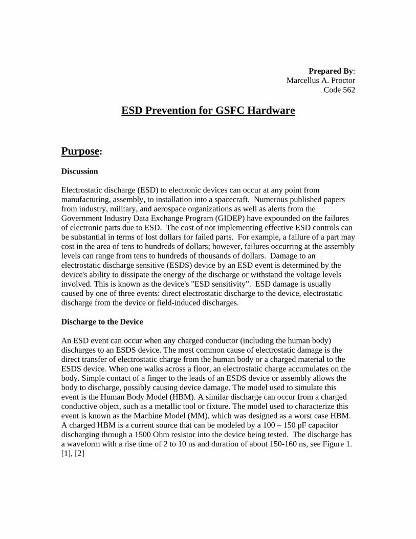
Discharge from the Device
The transfer of charge from an ESDS device, typically through the pin contacts, is also a concern. Static charge may accumulate on the ESDS device itself through handling or contact with packaging materials, worksurfaces, or machine surfaces. This frequently occurs when a device moves across a surface or vibrates in a package. The model used to simulate the transfer of charge from an ESDS device is referred to as the Charged Device Model (CDM). The CDM is an energy source that can discharge through its lead into another device of different potential. The rise time often is less than 0.5 ns, and the duration can be less than 2 ns, see Figure 1. [1], [2]
Figure 1. Idealized Current Waveforms of HBM & CDM [1]
Field Induced Discharges
Another event that can directly or indirectly damage devices is termed field induction. Whenever any object becomes electrostatically charged, there is an electrostatic field associated with that charge. If an ESDS device is placed in that electrostatic field, a charge may be induced on the device. If the device is then momentarily grounded while within the electrostatic field, a transfer of charge from the device occurs as a CDM event. If the device is removed from the region of the electrostatic field and grounded again, a second CDM event will occur as charge (of opposite polarity from the first event) is transferred from the device. [1], [3]
Failures
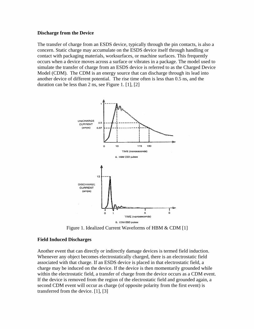
Many advanced technologies, such as Plastic Encapsulated Microcircuits (PEMs) for example, are susceptible at less than 100 volts and many disk drive components have sensitivities below 10 volts. To put more circuitry into small packages, the spacing isolating circuitry has been reduced making them more susceptible to ESD. A discharge of static electricity produces enough heat that can burn through microelectronic architecture that is rated to withstand voltage in the order of volts. Figure 2 shows the silicon thickness verses the mean ESD failure voltage of NMOSFETs.
ESD Failure Voltage vs. Silicon Film Thinkness
020406080
100120140160180200
400 600 650 760 810 1700
Thickness (Angstroms)
ESD
Fai
lure
Vol
tage
(V)
Voltage (V)
Figure 2. Mean ESD Failure Voltages of NMOSFET’s versus different silicon film thickness under positive ESD stress. [6]
ESD damages are generally classified as either a catastrophic failure or a latent defect.
Catastrophic Failure
When an electronic device is exposed to an ESD event, it may no longer function. The ESD event may have caused a metal melt, junction breakdown, or oxide failure. The device's circuitry is permanently damaged causing the device fail. Such failures usually can be detected when the device is tested before shipment. If the ESD event occurs after test, the damage will go undetected until the device fails in operation. [2], [3]
Latent Defect
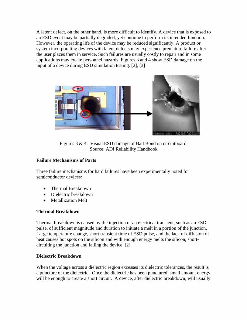
A latent defect, on the other hand, is more difficult to identify. A device that is exposed to an ESD event may be partially degraded, yet continue to perform its intended function. However, the operating life of the device may be reduced significantly. A product or system incorporating devices with latent defects may experience premature failure after the user places them in service. Such failures are usually costly to repair and in some applications may create personnel hazards. Figures 3 and 4 show ESD damage on the input of a device during ESD simulation testing. [2], [3]
Figures 3 & 4. Visual ESD damage of Ball Bond on circuitboard. Source: ADI Reliability Handbook
Failure Mechanisms of Parts Three failure mechanisms for hard failures have been experimentally noted for semiconductor devices:
Thermal Breakdown Thermal breakdown is caused by the injection of an electrical transient, such as an ESD pulse, of sufficient magnitude and duration to initiate a melt in a portion of the junction. Large temperature change, short transient time of ESD pulse, and the lack of diffusion of heat causes hot spots on the silicon and with enough energy melts the silicon, short-circuiting the junction and failing the device. [2] Dielectric Breakdown When the voltage across a dielectric region excesses its dielectric tolerances, the result is a puncture of the dielectric. Once the dielectric has been punctured, small amount energy will be enough to create a short circuit. A device, after dielectric breakdown, will usually
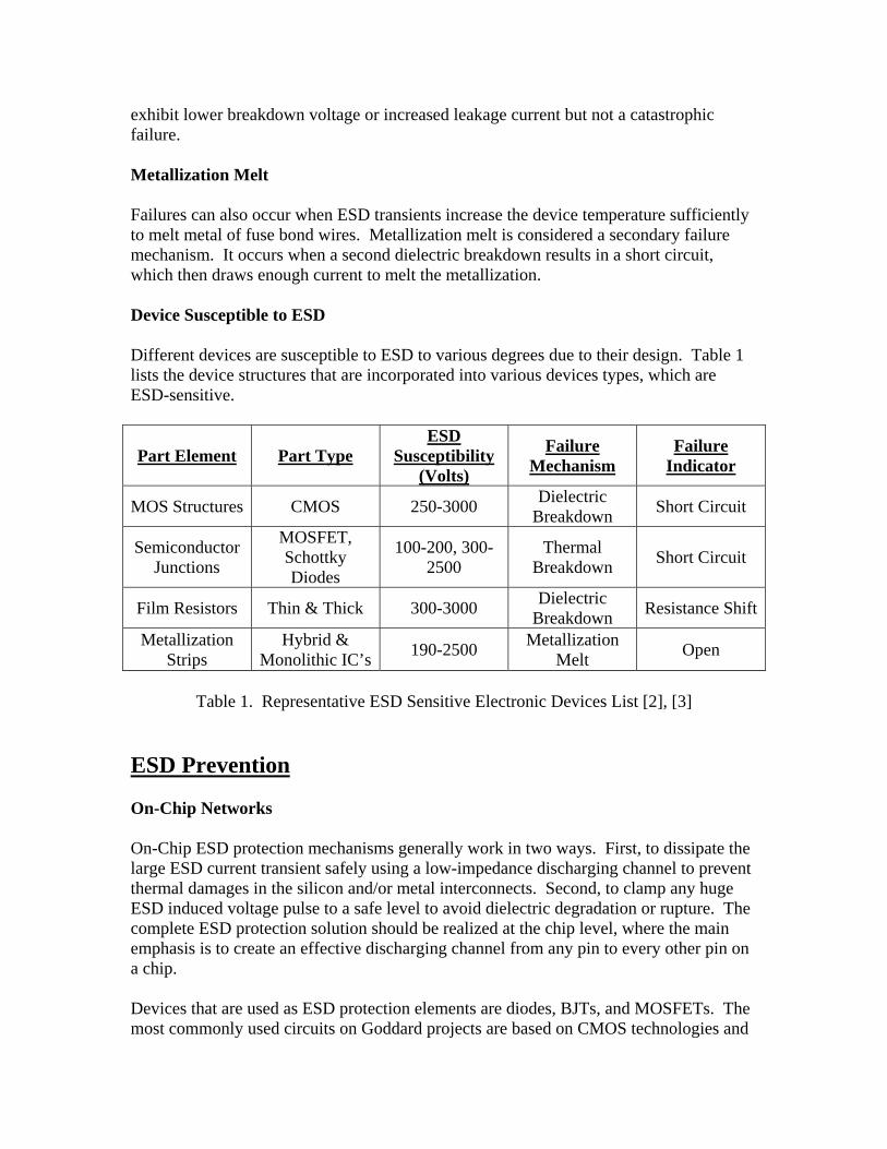
exhibit lower breakdown voltage or increased leakage current but not a catastrophic failure. Metallization Melt Failures can also occur when ESD transients increase the device temperature sufficiently to melt metal of fuse bond wires. Metallization melt is considered a secondary failure mechanism. It occurs when a second dielectric breakdown results in a short circuit, which then draws enough current to melt the metallization. Device Susceptible to ESD Different devices are susceptible to ESD to various degrees due to their design. Table 1 lists the device structures that are incorporated into various devices types, which are ESD-sensitive.
Part Element Part TypeESD
Susceptibility (Volts)
Failure Mechanism
Failure Indicator
MOS Structures CMOS 250-3000 Dielectric Breakdown Short Circuit
Semiconductor Junctions
MOSFET, Schottky Diodes
100-200, 300-2500
Thermal Breakdown Short Circuit
Film Resistors Thin & Thick 300-3000 Dielectric Breakdown Resistance Shift
Metallization Strips
Hybrid & Monolithic IC’s 190-2500 Metallization
Melt Open
Table 1. Representative ESD Sensitive Electronic Devices List [2], [3]
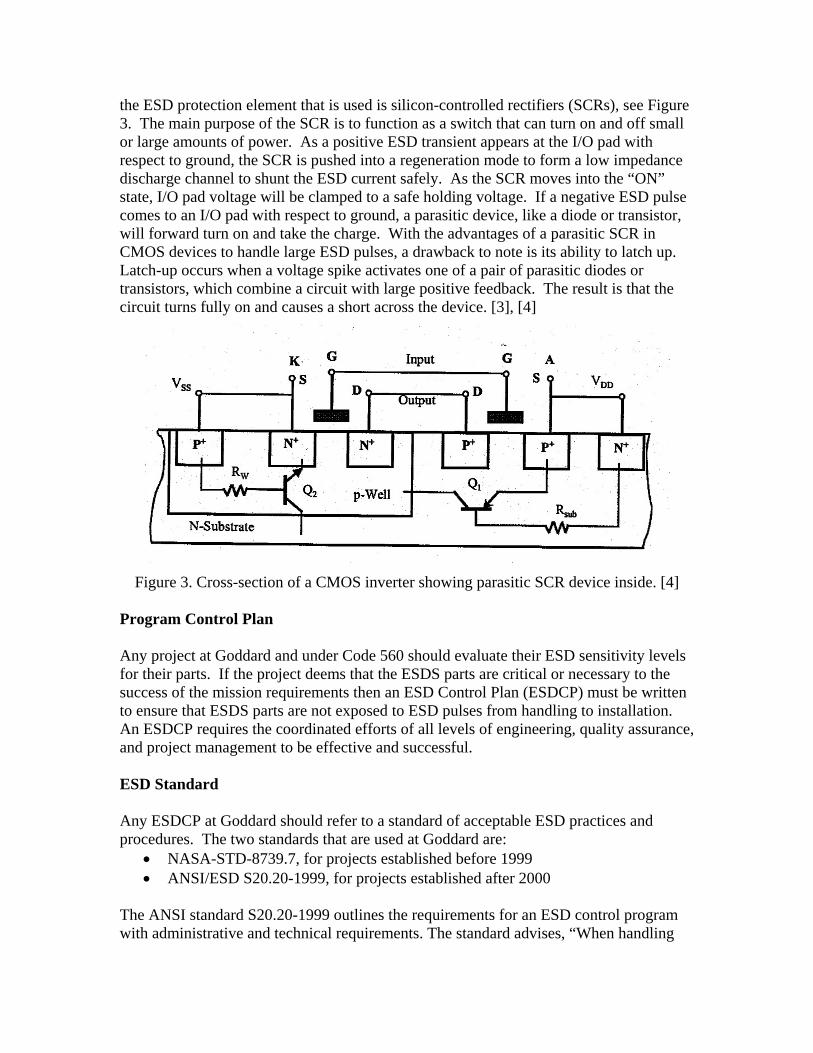
ESD Prevention On-Chip Networks On-Chip ESD protection mechanisms generally work in two ways. First, to dissipate the large ESD current transient safely using a low-impedance discharging channel to prevent thermal damages in the silicon and/or metal interconnects. Second, to clamp any huge ESD induced voltage pulse to a safe level to avoid dielectric degradation or rupture. The complete ESD protection solution should be realized at the chip level, where the main emphasis is to create an effective discharging channel from any pin to every other pin on a chip. Devices that are used as ESD protection elements are diodes, BJTs, and MOSFETs. The most commonly used circuits on Goddard projects are based on CMOS technologies and
the ESD protection element that is used is silicon-controlled rectifiers (SCRs), see Figure 3. The main purpose of the SCR is to function as a switch that can turn on and off small or large amounts of power. As a positive ESD transient appears at the I/O pad with respect to ground, the SCR is pushed into a regeneration mode to form a low impedance discharge channel to shunt the ESD current safely. As the SCR moves into the “ON” state, I/O pad voltage will be clamped to a safe holding voltage. If a negative ESD pulse comes to an I/O pad with respect to ground, a parasitic device, like a diode or transistor, will forward turn on and take the charge. With the advantages of a parasitic SCR in CMOS devices to handle large ESD pulses, a drawback to note is its ability to latch up. Latch-up occurs when a voltage spike activates one of a pair of parasitic diodes or transistors, which combine a circuit with large positive feedback. The result is that the circuit turns fully on and causes a short across the device. [3], [4]
Figure 3. Cross-section of a CMOS inverter showing parasitic SCR device inside. [4] Program Control Plan Any project at Goddard and under Code 560 should evaluate their ESD sensitivity levels for their parts. If the project deems that the ESDS parts are critical or necessary to the success of the mission requirements then an ESD Control Plan (ESDCP) must be written to ensure that ESDS parts are not exposed to ESD pulses from handling to installation. An ESDCP requires the coordinated efforts of all levels of engineering, quality assurance, and project management to be effective and successful. ESD Standard Any ESDCP at Goddard should refer to a standard of acceptable ESD practices and procedures. The two standards that are used at Goddard are:
• NASA-STD-8739.7, for projects established before 1999 • ANSI/ESD S20.20-1999, for projects established after 2000
The ANSI standard S20.20-1999 outlines the requirements for an ESD control program with administrative and technical requirements. The standard advises, “When handling
devices susceptible to less than 100 volts HBM (Human Body Model), more stringent ESD Control Program Technical Requirements may be required, including adjustment of program Technical Element Recommended Ranges.” In other words, it is up to the project to define the level of ESD protection required and develops acceptable minimum standards for control devices. Using the NASA-STD-8739.7 would be a good template in defining ESD protection requirements for a project. Training Plan A project that has identified that they will be using ESDS parts should invest in developing a training plan. Any personnel who will be working on ESDS parts or doing maintenance work in facilities that are designated as ESD protected areas, must be ESD certified. ESD certification classes are offered through the NASA Manufacturing Technology Transfer Center (NMTTC) or another facility, which is NASA certified to instruct in ESD protocols.
Protected Areas
The primary function of an ESD protected area is to reduce static withstand voltage levels of ESDS parts. Caution signs must clearly denote to alert personnel that the area is ESD controlled. The below items are what a typical ESD protected area should have and their resistance or voltage recommended limits: [1], [2]
• Work Surface/Mats: <1 x 10⁹ Ohm • Wrist Strap: 0.8 x 10⁶ to 1.2 x 10⁶ Ohm • Foot Strap: 0.8 x 10⁶ to 1.2 x 10⁶ Ohm • Conductive Flooring: 1 x 10⁵ to 1 x 10¹¹ Ohm. • Seating: <1 x 10⁷ Ohm. • Bags: <1 X 10⁸ Ohm • Ionization (other than room systems): <± 50 V offset. • Ionization (room system): <± 150 V offset. • Protected Garments: 1 x 10⁵ to 1 x 10¹¹ Ohm. • AC Power Tools: < 1 Ohm • Battery Power Tools: < 1 x 10¹² Ohm
Organizational Responsibilities In developing any ESDCP the following organizations within Goddard are essential in preventing ESD: [2]
1. Project Quality Assurance (Code 400 & 300)
a. Oversee ESD awareness and certification training for all personnel working or have access to an ESD sensitive area.
b. Maintain work instructions, drawings, and other documentation for ESD cautions, markings, and precautionary procedures.
c. Audit and certify ESD-protected areas on a regular basis. Frequency should be stated by application of project (refer to NASA-STD-8739.7 Table 7-1).
d. Ensure that access to protected areas be limited to persons who have completed ESD training.
e. Communication between personnel, ESD monitors, and project managers is essential in ensuring that parts are functional and not damage from ESD.
2. Parts Engineering (Code 562)
a. Parts Engineer identifies and classifies ESD sensitivity levels of parts. If sensitivity level is unknown, Parts Analysis Laboratory has ESD sensitivity tester, which can determine sensitivity level using HBM, MM, CDM.
b. Parts Engineer selects parts with lowest ESD sensitivity, if possible. If not, verify that ESD protection circuitry is in place.
c. Perform and assist in failure analysis of ESD sensitive items. d. Collect and maintain part ESD sensitivity data from supply vendors and
manufacturers. e. New technologies and correction of discovered deficiencies database be
maintained. f. Document ESD procedures in Work Instructions (WIs) and maintain
Procedure Guidelines (PG) for Code 562. g. Certify that technicians, engineers, and authorized personnel in test labs
are ESD trained.
3. Packaging and Shipping (Code 239) a. Parts that are received, stored, kitted, or ship for Goddard projects will be
handled by Code 239. b. Implement ESD precautionary handling and packaging procedures during
receiving, processing, inspection, and packaging. If there is an issue with packaging an ESDS part, inform Parts Engineer for assistance.
c. Package ESD sensitive items in ESD/moisture protective material for handling and shipment.
d. ESDS assemblies, parts, and equipment must be marked with an ESD caution symbol in a readily visible position. ESD protective packaging should be marked.
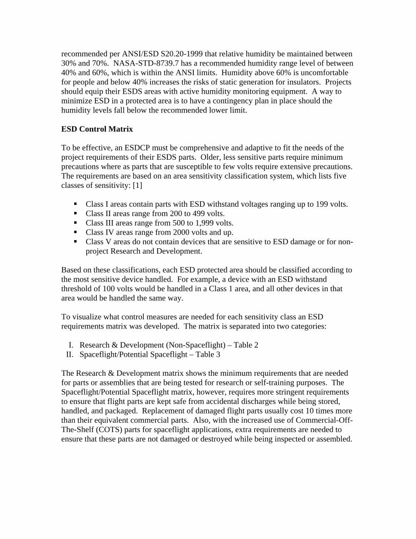
Humidity Levels Humidity is an important factor in the generation of static electricity. As humidity increases, the surface resistivity decreases. This condition means that insulator materials rubbed together or pulled apart in a humid environment generate lower static charges than the same materials rubbed together or pulled apart in a dry environment. It is
recommended per ANSI/ESD S20.20-1999 that relative humidity be maintained between 30% and 70%. NASA-STD-8739.7 has a recommended humidity range level of between 40% and 60%, which is within the ANSI limits. Humidity above 60% is uncomfortable for people and below 40% increases the risks of static generation for insulators. Projects should equip their ESDS areas with active humidity monitoring equipment. A way to minimize ESD in a protected area is to have a contingency plan in place should the humidity levels fall below the recommended lower limit. ESD Control Matrix To be effective, an ESDCP must be comprehensive and adaptive to fit the needs of the project requirements of their ESDS parts. Older, less sensitive parts require minimum precautions where as parts that are susceptible to few volts require extensive precautions. The requirements are based on an area sensitivity classification system, which lists five classes of sensitivity: [1] Class I areas contain parts with ESD withstand voltages ranging up to 199 volts. Class II areas range from 200 to 499 volts. Class III areas range from 500 to 1,999 volts. Class IV areas range from 2000 volts and up. Class V areas do not contain devices that are sensitive to ESD damage or for non-
project Research and Development. Based on these classifications, each ESD protected area should be classified according to the most sensitive device handled. For example, a device with an ESD withstand threshold of 100 volts would be handled in a Class 1 area, and all other devices in that area would be handled the same way. To visualize what control measures are needed for each sensitivity class an ESD requirements matrix was developed. The matrix is separated into two categories:
I. Research & Development (Non-Spaceflight) – Table 2 II. Spaceflight/Potential Spaceflight – Table 3
The Research & Development matrix shows the minimum requirements that are needed for parts or assemblies that are being tested for research or self-training purposes. The Spaceflight/Potential Spaceflight matrix, however, requires more stringent requirements to ensure that flight parts are kept safe from accidental discharges while being stored, handled, and packaged. Replacement of damaged flight parts usually cost 10 times more than their equivalent commercial parts. Also, with the increased use of Commercial-Off-The-Shelf (COTS) parts for spaceflight applications, extra requirements are needed to ensure that these parts are not damaged or destroyed while being inspected or assembled.
Class I Class II Class III Class IV Class VESD
Program Plan
NR NR NR NR NR
Personnel Training OP OP OP OP NR
Auditing NR NR NR NR NR Protected
Workstations OP OP OP OP NR
Wrist Strap R R R R NR Protective Clothing OP OP OP OP NR
Conductive Floors NR NR NR NR NR
Ionizers NR NR NR NR NR Foot Straps NR NR NR NR NR Humidity Monitors OP OP OP OP NR
Protective Bags R R R R NR
Work Mats R R R R NR Sensitivity Marking OP OP OP OP NR
Sensitivity Testing NR NR NR NR NR
Finger Cots NR NR NR NR NR Seats NR NR NR NR NR
Storage Equipment NR NR NR NR NR
R = Required OP = Optional (Consult Project) NR = Not Required
Table 2. ESD Requirements Matrix for Research & Development Applications
Class I Class II Class III Class IV Class VESD
Program Plan
R R R R NR
Personnel Training R R R R NR
Auditing R R R R NR Protected
Workstations R R R R NR
Wrist Strap R R R R NR
Protective Clothing R R R R NR
Conductive Floors R R R OP NR
Ionizers OP OP OP OP NR Foot Straps OP OP OP OP NR Humidity Monitors R R R R NR
Protective Bags R R R R NR
Work Mats R R R R NR Sensitivity Marking R R R R NR
Sensitivity Testing OP OP OP OP NR
Finger Cots OP OP OP OP NR Seats OP OP OP OP NR
Storage Equipment R R R R NR
R = Required OP = Optional (Consult Project) NR = Not Required
Table 3. ESD Requirements Matrix for Spaceflight/Potential Spaceflight Applications
Recommendation
To be effective, every project should assess their ESD requirements and determine what level of precaution is necessary to ensure that their ESDS parts are protected. An effective ESD control program must be comprehensive and documented into a work instruction and procedures document that encompasses the processes controls, personnel training, and ESD-susceptible device protection. This plan must be adjusted to suit each project specific needs, but should follow basic guidelines set forth by ANSI/ESD S20.20-1999. To coordinate all ESD activities within a project, a person or a team of people should be appointed, by the project, to oversee all ESD related issues and have regular contact with Project Managers. In addition, management support, personnel training, and routine follow-up audits are part of an effective ESDCP. This paper serves as a starting point for projects to ensure that their ESDS parts are protected. By following the points laid out in this paper, projects at Goddard and in Code 560 can make ESD control programs into a competitive advantage—a strategic tool focused on quality, productivity, and customer satisfaction.
Reference 1. Dangelmayer, G. Theodore, “ESD Program Management”, Kluwer Academic
Publishers, 1999 2. Bhar, Tarak N. & McMahon, Edward J., “Electrostatic Discharge Control”, Hayden
Book Company, 1983 3. Matisoff, Bernard S., “Handbook of Electrostatic Discharge Controls”, Van Nostrand
Reinhold Company, 1986 4. Wang, Albert Z. H., “On-chip ESD Protection for Integrated Circuits”, Kluwer
Academic Publishers, 2002 5. Dabral, Sanjay & Maloney, Timothy J., “Basic ESD and I/O Design”, John Wiley &
Son, Inc., 1998 6. Chan, Mansun & Ko, Ping K. “ESD Reliability and Protection Schemes in SOI
CMOS Output Buffers”, IEEE Transactions on Electron Devices, Vol. 42, No. 10, p. 1819, October 1995