27
pushing the envelope of PA efficiency ET Envelope Path from digits to PA Gerard Wimpenny Nujira Ltd ARMMS Conference 19 th /20 th November 2012
| Date post: | 21-May-2018 |
| Category: |
Documents |
| Upload: | duongthuan |
| View: | 214 times |
| Download: | 1 times |

pushing the envelope of PA efficiency
ET Envelope Pathfrom digits to PA
Gerard WimpennyNujira Ltd
ARMMS Conference19th/20th November 2012

2
Agenda
• Envelope Processing• ET PA Characterisation• Isogain shaping• CFR shaping
• Envelope Amplifier Design Requirements• Sources of Impairment• Integrated Modulator• Distributed Modulator
3
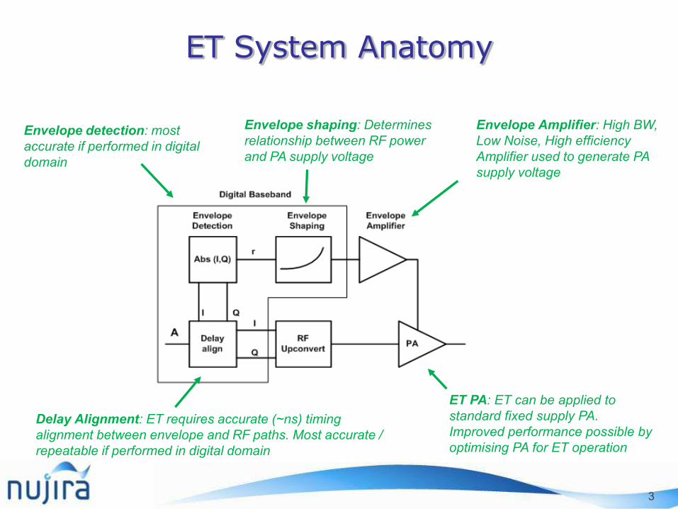
ET System Anatomy
Envelope detection: mostaccurate if performed in digitaldomain
Envelope shaping: Determinesrelationship between RF powerand PA supply voltage
Envelope Amplifier: High BW,Low Noise, High efficiencyAmplifier used to generate PAsupply voltage
ET PA: ET can be applied tostandard fixed supply PA.Improved performance possible byoptimising PA for ET operation
Delay Alignment: ET requires accurate (~ns) timingalignment between envelope and RF paths. Most accurate /repeatable if performed in digital domain
4
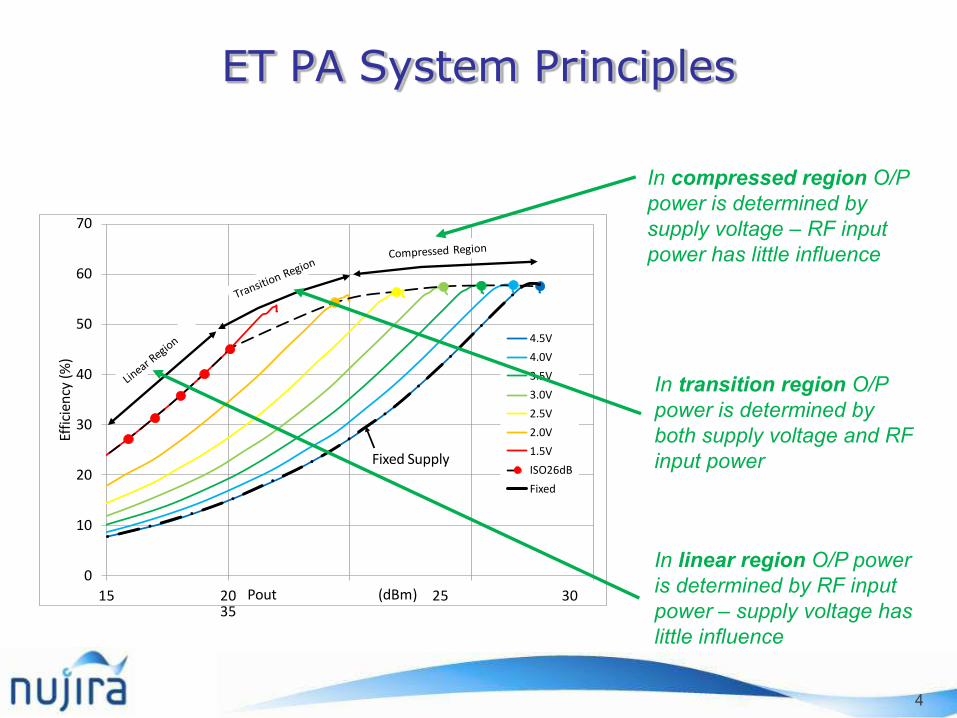
ET PA System Principles
0
10
20
30
40
50
60
70
15 20 Pout (dBm) 25 3035
Effic
ienc
y (%
)
4.5V4.0V3.5V3.0V2.5V2.0V1.5VISO26dBFixed
Fixed Supply
In compressed region O/Ppower is determined bysupply voltage – RF inputpower has little influence
In linear region O/P poweris determined by RF inputpower – supply voltage haslittle influence
In transition region O/Ppower is determined byboth supply voltage and RFinput power
5
-1.5
-1
-0.5
0
0.5
1
1.5
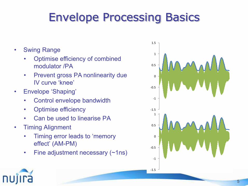
Envelope Processing Basics
• Swing Range• Optimise efficiency of combined
modulator /PA• Prevent gross PA nonlinearity due
IV curve ‘knee’• Envelope ‘Shaping’
• Control envelope bandwidth• Optimise efficiency• Can be used to linearise PA
• Timing Alignment• Timing error leads to ‘memory
effect’ (AM-PM)• Fine adjustment necessary (~1ns)
-1.5
-1
-0.5
0
0.5
1
1.5
-1.5
-1
-0.5
0
0.5
1
1.5
-1.5
-1
-0.5
0
0.5
1
1.5
-1.5
-1
-0.5
0
0.5
1
1.5

6
PA Characterisation Methods
Testmethodology
PA currentmeasurement
Supplyimpedance
Supplybandwidth
requirements
ETEfficiencyprediction
ET Linearityprediction
Parametersmeasured
SweptCW testing Bench PSU
Low(decouplingCapacitor)
Low (BenchPSU)
Poor, due toPA dieheating
Poor, due toPA dieheating
Gain (AM:AM),Efficiency
Pulsed RF /DCtesting
Instrumentationgrade current
probe,~5 us resolution
Low(decouplingCapacitor)
Low (BenchPSU)
Good, if shortpulses (~10
us, 10% dutycycle).
Fair(if device haslow AM/PM)
Gain (AM:AM),Efficiency
Dynamicsupply
modulation
Challenging –high BW withhigh commonmode voltagecurrent sense
Requires lowimpedance
dynamic supply(no decoupling)
High(~60 MHz BW) V. Good
V. Good(if device haslow memory
effects)
Gain (AM:AM),Phase (AM:PM),
Efficiency
Phase measurement possible in principle – but accuracy poor dueto heating effects and phase reference ‘wander’
No phasemeasurement
PA Characteristics must be known to determine Shaping table

7
AM/PM Input Surfaces
Input Gain Surface Input Phase Surface
Fixed Supply VoltageGain contours
Fixed Supply VoltagePhase contours

8
Isogain Contours
25dB IsoGainshaping contour
27dB IsoGainshaping contour
Low voltage phasecollapse
Phase peak flatteningc.f. fixed supply
Input Gain Surface Input Phase Surface
9
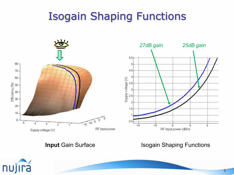
Isogain Shaping Functions
Isogain Shaping Functions
27dB gain 25dB gain
Input Gain Surface
10
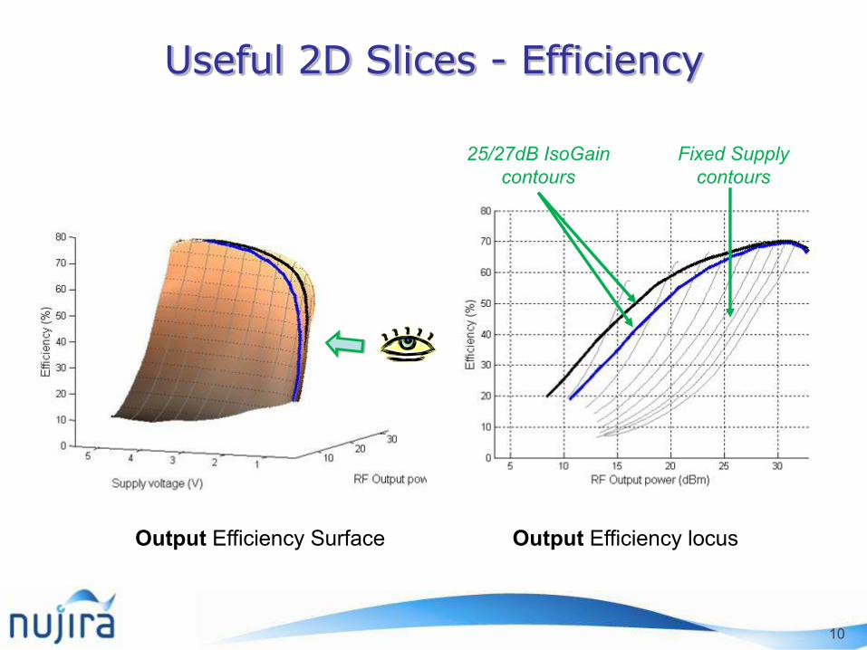
Useful 2D Slices - Efficiency
Output Efficiency Surface Output Efficiency locus
25/27dB IsoGaincontours
Fixed Supplycontours

11
2D Slices AM/AM, AM/PM
AM/AM distortion removed Residual PM distortion
Output Gain Output Phase
12
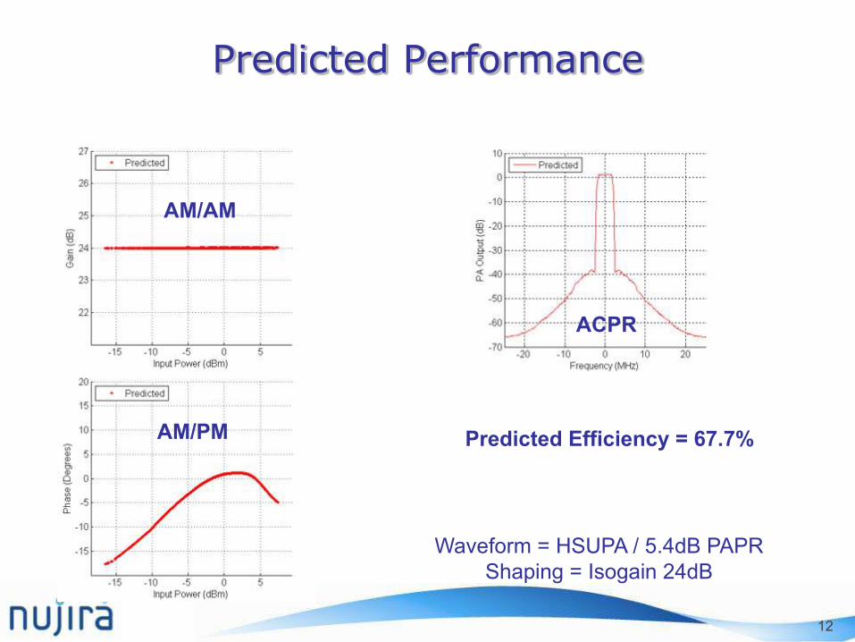
Predicted Performance
ACPR
AM/PM
AM/AM
Predicted Efficiency = 67.7%
Waveform = HSUPA / 5.4dB PAPRShaping = Isogain 24dB

13
Measured Performance
ACPR
AM/PM
AM/AM
Predicted Efficiency = 67.7%Measured Efficiency = 67.6%
Waveform = HSUPA / 5.4dB PAPRShaping = Isogain 24dB

14
Shaping Table based CFR
Isogain shaping modified to introduce softclipping e.g using ‘Rapp’ function (VCFR)
Desired PA gain profile p p
Vpk
iso
V isoV CFR =
V1
1 ÷÷
ø
ö
çç
è
æ
÷÷ ø
öçç è
æ+ V Limiting voltage
factorSmoothnessp =
pk =
Unmodified Isogainshaping (Viso)
Envelope AmplifierMax Vout
15
0 1 2 3 4 5 6 710-4
10-3
10-2
10-1
100
dB above mean
Pro
babi
lity
0 1 2 3 4 5 6 710-4
10-3
10-2
10-1
100
dB above mean
Pro
babi
lity
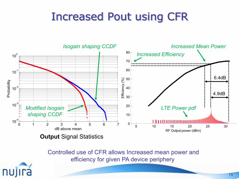
Increased Pout using CFR
5 10 15 20 25 300
10
20
30
40
50
60
70
80
RF Output power (dBm)
Effi
cien
cy (%
) 6.4dB
4.9dB
Output Signal Statistics
Isogain shaping CCDF
Modified Isogainshaping CCDF
Increased Mean Power
LTE Power pdf
Controlled use of CFR allows Increased mean power andefficiency for given PA device periphery
Increased Efficiency

16
-200 1 2 3 4 x 10
7
-10
0
10
20
30
40
50
60
70
80
Offset from Carrier (Hz)
PS
D (d
B)
Reference Spectrum(No clipping)
‘Software Defined PA’RF Spectrum
0 2 4
x 107
-20
0
20
40
60
80
0 2 4
x 107
-20
0
20
40
60
80
0 2 4 x 10⁷-20
0
20
40
60
80
0 2 4
x 107
-20
0
20
40
60
80
0 2 4
x 107
-20
0
20
40
60
80
0 2 4
x 107
-20
0
20
40
60
80
0 2 4 x 10⁷-20
0
20
40
60
80
0 2 4
x 107
-20
0
20
40
60
80
Hard clippingSoft clipping
75% Clipping level(2.5dB CFR)
85% Clipping level(1.4dB CFR)
p=4 p=6 p=10 p=100
Shaping Table based CFR allows dynamic configuration of PA’sPower / ACPR / Efficiency characteristics
Offset from Carrier (Hz)
PS
D (d
B)

17
Agenda
• Envelope Processing• ET PA Characterisation• Isogain shaping• CFR shaping
• Envelope Amplifier Design Requirements• Sources of Impairment• Integrated Modulator• Distributed Modulator

18
Envelope AmplifierRequirements
High Bandwidth(e.g 4ch WCDMA, 20MHz LTE, 2x 10MHz WiMAX)• Envelope Bandwidth ~3x RF Bandwidth• Cannot be achieved with ‘switcher only’
architectureLow Noise / Distortion
• Required to meet ACPR specifications• Many factors to consider• Requires high Tracking Accuracy
High Efficiency• Must consider combined PA / modulator
efficiency• Linear supply would be pointless
Power• Must maintain BW and Noise at
increased power levels
Low Noise
HighBandwidth
HighEfficiency
Power
19
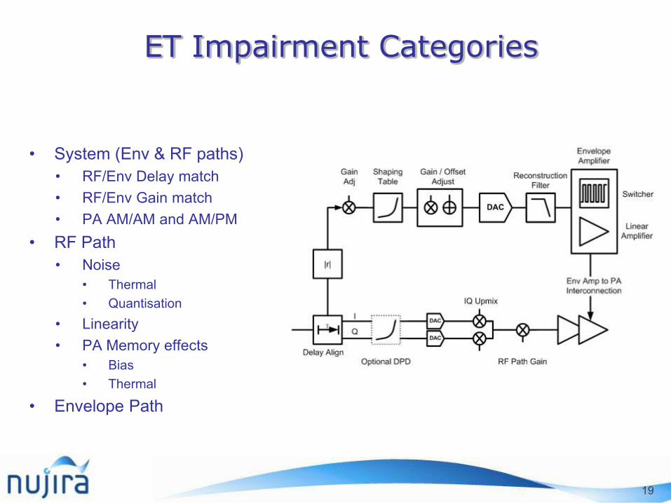
ET Impairment Categories
• System (Env & RF paths)• RF/Env Delay match• RF/Env Gain match• PA AM/AM and AM/PM
• RF Path• Noise
• Thermal• Quantisation
• Linearity• PA Memory effects
• Bias• Thermal
• Envelope Path
20
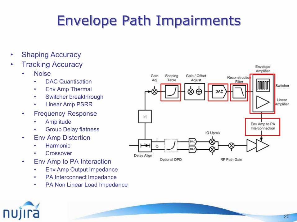
Envelope Path Impairments
• Shaping Accuracy• Tracking Accuracy
• Noise• DAC Quantisation• Env Amp Thermal• Switcher breakthrough• Linear Amp PSRR
• Frequency Response• Amplitude• Group Delay flatness
• Env Amp Distortion• Harmonic• Crossover
• Env Amp to PA Interaction• Env Amp Output Impedance• PA Interconnect Impedance• PA Non Linear Load Impedance

21
Tracking Accuracy Explained
• The difference between ideal and measured supply waveform after removalof DC offset, gain and timing errors
• Analogous to EVM for modulated signals• Tracking error analysis is useful diagnostic tool: RMS, Peak, Spectrum
0
10
20
30
40
50
60
V
-10-8-6-4-202468
10
V
0
10
20
30
40
50
60
V
-10-8-6-4-202468
10
V
-10-8-6-4-202468
10
V
-10-8-6-4-202468
10
V
0
10
20
30
40
50
60
V
0
10
20
30
40
50
60
V
Gross gain and timing errorGross timing errorSmall timing errorResidual modulator tracking error
Ideal and measured waveforms Tracking Error

22
Supply ‘Noise’ – RF Conversion
• PA in compression – Supply Noise & Distortion modulates RF carrier• PA can be considered as mixer
• O/P spectrum is convolution of Supply and PA input Spectra
• Conversion factor (Supply Sensitivity) for noise on supply to RFsidebands is similar to ideal AM modulator (mixer)
0
-10
-20
-30
-40
-50
-60
-70
-80
-90
-100Start: 0 Hz Stop: 200.0000 MHz
12-1
0
-10
-20
-30
-40
-50
-60
-70
-80
-90
-100Start: 1.8500 GHz Stop: 2.0500 GHz
1
2-1
3 4-35 6-5
40MHz ‘test tone’ added to Envelope Amplifier O/P(whilst amplifying 5MHz WCDMA signal)
Corresponding RF sidebands
40MHz
40MHz
Supply Spectrum RF Spectrum

23
Measured Supply Sensitivity
Average DC drain voltage 2.62VMeasured 40MHz injected tone level 17.3mV rmsCalculated RF sideband level for ideal AM modulator -49.6dBCMeasured RF sideband level -51dBCPA Supply Sensitivity (dB) -1.4dBPA Supply Sensitivity (%) 85%
An ideal AM modulator is described by:
where modulation index
This can be re-expressed in terms of carrier and LSB and USB components
where for an ideal AM modulator
env
env
rf
rf
VDVV
DV
env
env
VDV
rf
rf
VDV
)sin()]cos([)y(t = A+ M wmt wct
AMh =
)])sin(())[sin(()sin()y(t = A wct + R wc +wm t + wc -wm t
2MR =
24
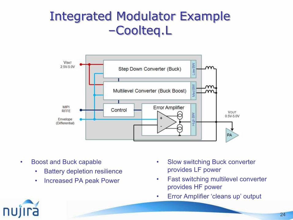
Integrated Modulator Example–Coolteq.L
• Slow switching Buck converterprovides LF power
• Fast switching multilevel converterprovides HF power
• Error Amplifier ‘cleans up’ output
• Boost and Buck capable• Battery depletion resilience• Increased PA peak Power

25
Distributed Modulator Example- Coolteq.u
RF S
PLITTER
RF C
OM
BIN
ER
Coolteq.uPowerSupplyModule(PSM)
PA
HAT
PA
HAT
PA
HAT
PA
HAT
RFDriver
RF [email protected] dB
PAPR
RF in
Envelopesignal
generation
DigitalPre
Distortion
RFUpconvert
Exciter
Modulation
Envelopeinput
DCinput
4 x Coolteq.u High Accuracy Tracking module (HAT®) • Scalable O/P Power• Allows multiple PAs per
Power Supply Module(PSM)
• Allows Envelope pathLinear Amplifier to beplaced close to PA
• PA supply impedanceminimised

26
Conclusions
• Understanding of PA characteristics key toachieving good ET performance.
• Careful selection of shaping table contentsallows optimisation key ET system performancemetrics
• ET is a simple concept, but attention must bepaid to multiple potential sources of impairmentto realise full potential

pushing the envelope of PA efficiency


![[SCORE] Opus 76 Pout-pourri (Guitar & Flute or Violin)](https://static.documents.pub/doc/80x56/5695d2781a28ab9b029a8a98/score-opus-76-pout-pourri-guitar-flute-or-violin.jpg)

![New Doc 04-02-2020 07.31 - WordPress.com · [Gandaan keseluruhan, At (dB) bagi radio penerima AM.] The output power, Pout in Watts and dBm. [Kuasa keseluruhan, Pout dalam Watt dan](https://static.documents.pub/doc/80x56/5f6479ece50ca6114d31f430/new-doc-04-02-2020-0731-gandaan-keseluruhan-at-db-bagi-radio-penerima-am.jpg)