Rev. C Evaluation boards are only intended for device evaluaEvaluation boards are supplied “as is” and without warrastatutory including, but not limited to, any implied warraparticular purpose. No license is granted by implication orintellectual property by application or use of evaluation boDevices is believed to be accurate and reliable. However, nDevices for its use, nor for any infringements of patents or otfrom its use. Analog Devices reserves the right to changewithout notice. Trademarks and registered trademarks areEvaluation boards are not authorized to be used in life suppor
ox 9106, Norwood, MA 02062-9106, U.S.A.www.analog.com
2009 Analog Devices, Inc. All rights reserved.
tion and not for production purposes. nties of any kind, express, implied, or nty of merchantability or fitness for a otherwise under any patents or other ards. Information furnished by Analog o responsibility is assumed by Analog
her rights of third parties that may result devices or specifications at any time
the property of their respective owners. t devices or systems.
FEATURES Powerful companion design tool for quick design times Input voltage range: 3.15 V to 14 V Output voltage range: 0.8 V to VIN
Output current: up to 10 A Accommodating layout with multiple packages for diodes,
PFETs, input and output capacitors, and inductors 3 PFETs in parallel for high current applications Programmable compensation for optimizing transient
performance Programmable current limit with sense resistor(s) Enable/shutdown logic Switching frequency: 580 kHz Kelvin connections for measuring input and output voltage
Input voltage range: 9 V to 12 V Output voltage: 3.3 V Output current: 3 A
Bare board ADP1864-BL-EVALZ Populated with only ADP1864
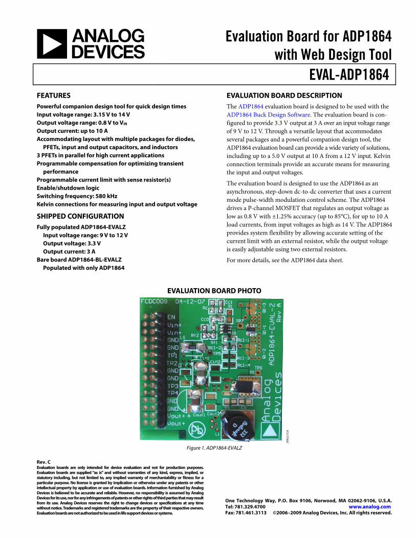
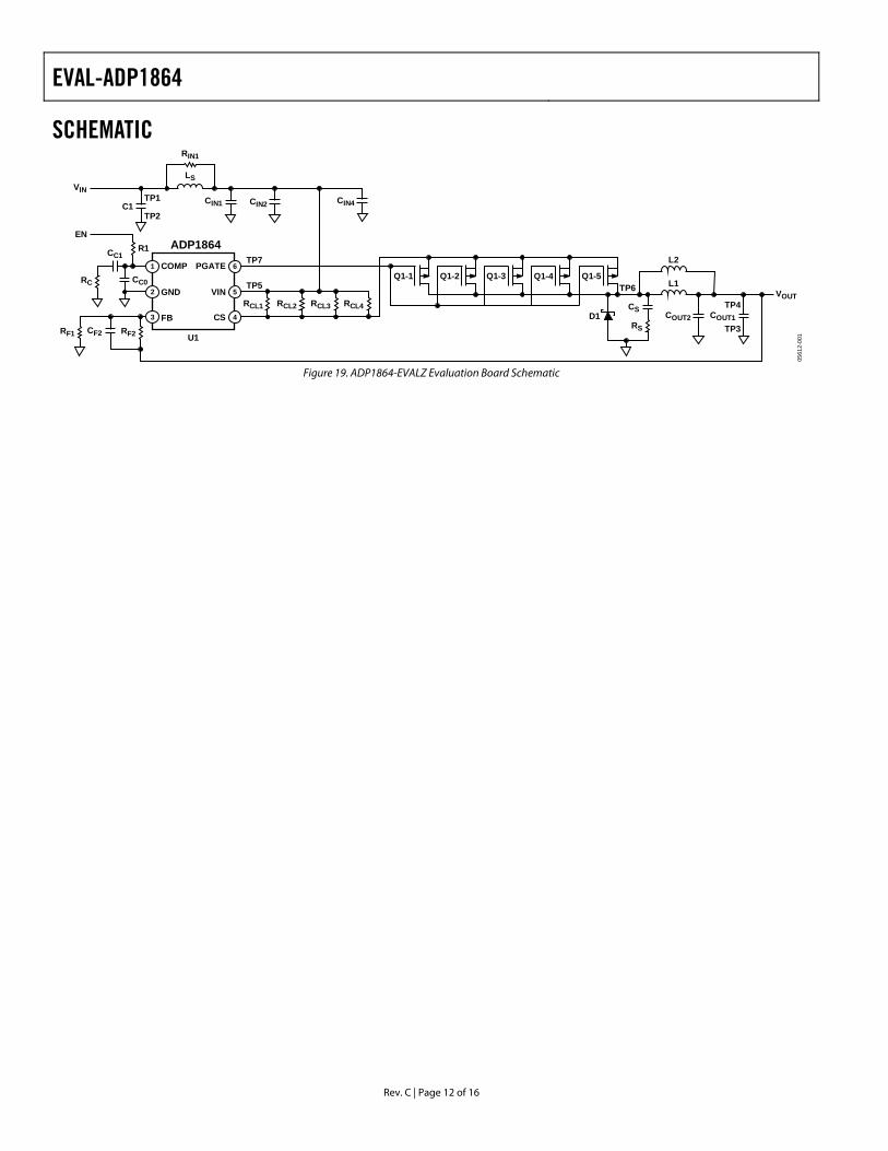
EVALUATION BOARD DESCRIPTION The ADP1864 evaluation board is designed to be used with the ADP1864 Buck Design Software. The evaluation board is con-figured to provide 3.3 V output at 3 A over an input voltage range of 9 V to 12 V. Through a versatile layout that accommodates several packages and a powerful companion design tool, the ADP1864 evaluation board can provide a wide variety of solutions, including up to a 5.0 V output at 10 A from a 12 V input. Kelvin connection terminals provide an accurate means for measuring the input and output voltages.
The evaluation board is designed to use the ADP1864 as an asynchronous, step-down dc-to-dc converter that uses a current mode pulse-width modulation control scheme. The ADP1864 drives a P-channel MOSFET that regulates an output voltage as low as 0.8 V with ±1.25% accuracy (up to 85°C), for up to 10 A load currents, from input voltages as high as 14 V. The ADP1864 provides system flexibility by allowing accurate setting of the current limit with an external resistor, while the output voltage is easily adjustable using two external resistors.
REVISION HISTORY 7/09—Rev. B to Rev. C Changes to Changing the Output Voltage Section, Equation .. 11
6/08—Rev. A to Rev. B
Changes to Shipped Configuration Section .................................. 1 Changes to Figure 1 .......................................................................... 1 Changes to Powering the Evaluation Board Section ................... 3 Changes to Figure 3 Caption ........................................................... 4 Changes to Excel Design Tool Interface Section Heading .......... 8 Changes to Figure 18 Caption ......................................................... 8 Changes to BOM Summary Section .............................................. 9 Changes to Changing the Output Capacitors Section ............... 10 Changes to Figure 19 ...................................................................... 12 Added Figure 20 and Figure 21..................................................... 13 Changes to Table 1 .......................................................................... 14 Added Table 2 .................................................................................. 14 Changes to Ordering Guide .......................................................... 14
6/07—Rev. 0 to Rev. A
4/06—Revision 0: Initial Version
EVAL-ADP1864
Rev. C | Page 3 of 16
POWERING THE EVALUATION BOARD The ADP1864 evaluation board is supplied fully assembled or, optionally, populated with only the ADP1864 IC. Before applying power to the evaluation board, refer to Figure 2 and follow the procedures in this section.
INPUT POWER SOURCE Before connecting the power source to the ADP1864 evaluation board, make sure that it is turned off. If the input power source includes a current meter, use that meter to monitor the input current. Connect the positive terminal of the power source to the VIN terminal on the evaluation board, and the negative terminal of the power source to the GND terminal just below the VIN terminal. If the power source does not include a current meter, connect a current meter in series with the input source voltage. Connect the positive lead (+) of the power source to the ammeter positive (+) connection, the negative lead (−) of the power source to the GND terminal just below the VIN terminal on the evaluation board, and the negative lead (−) of the ammeter to the VIN terminal on the board.
OUTPUT LOAD Although the ADP1864 evaluation board can sustain the sudden connection of the load, it is possible to damage the load if it is not properly connected. Make sure that the board is turned off before connecting the load. If the load includes an ammeter, or if the current is not measured, connect the load directly to the evaluation board with the positive (+) load connection to the VOUT terminal and the negative (−) load connection to the GND terminal just above the VOUT terminal. If an ammeter is used, connect it in series with the load; connect the positive (+)
ammeter terminal to the evaluation board VOUT terminal, the negative (−) ammeter terminal to the positive (+) load terminal, and the negative (−) load terminal to the evaluation board GND terminal just above the VOUT terminal.
After the load is connected, make sure that it is set to the proper current before powering the ADP1864 evaluation board.
INPUT AND OUTPUT VOLTMETERS Measure the input and output voltages with voltmeters. Connect the voltmeter measuring the input voltage with the positive lead (+) connected to TP1 and the negative lead (−) connected to TP2. Connect the voltmeter measuring the output voltage with the positive lead (+) connected to TP4 and the negative lead (−) connected to TP3. Make sure to connect the voltmeters to the appropriate evaluation board terminals and not to the load or power source themselves. If the voltmeters are not connected directly to the evaluation board at these Kelvin connection test points (TP1 to TP4), the measured voltages will be incorrect due to the voltage drop across the leads connecting the evaluation board to both the source and load.
TURNING ON THE EVALUATION BOARD After the power source and load are connected to the ADP1864 evaluation board, the board can be powered for operation. Slowly increase the input power source voltage until the input voltage exceeds the minimum input operating voltage of 9 V. If the load is not already enabled, enable the load and check that it is drawing the proper current and that the output voltage maintains voltage regulation.
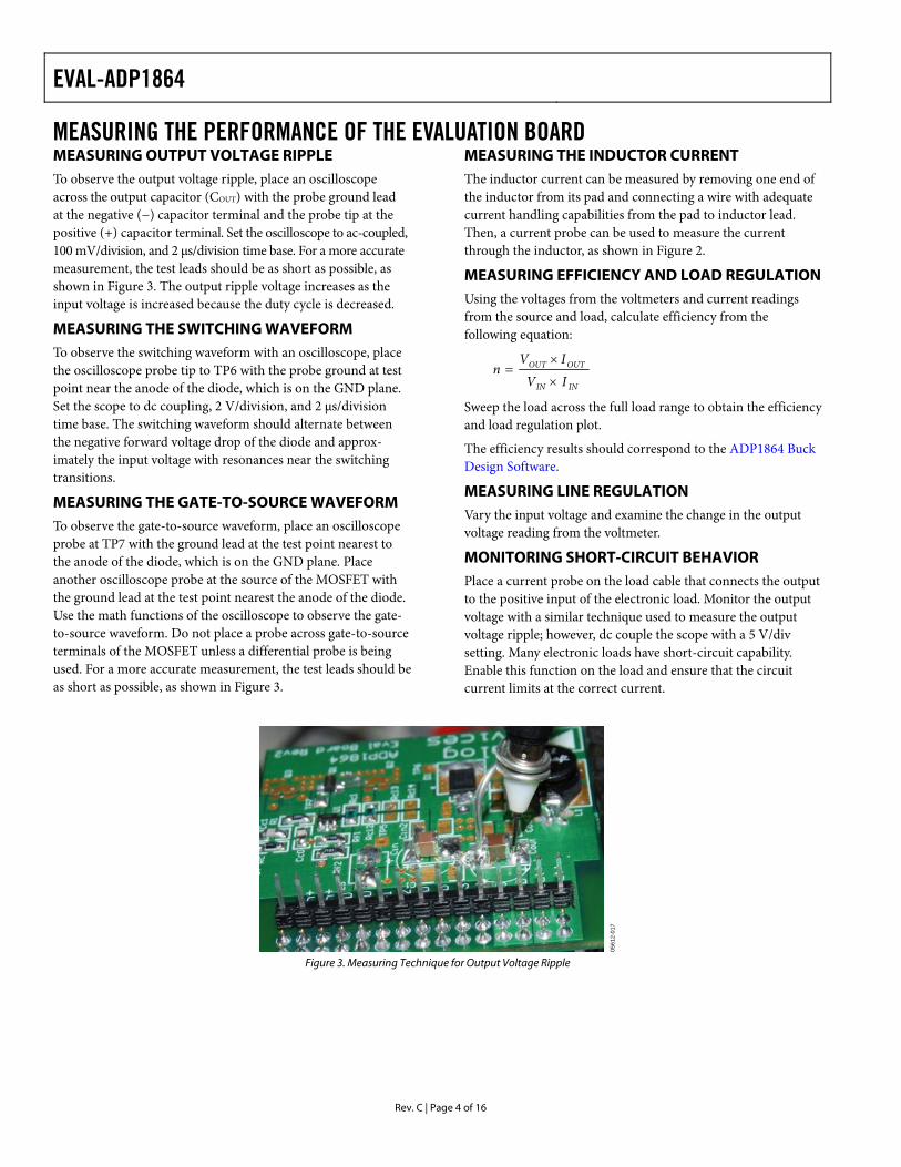
MEASURING THE PERFORMANCE OF THE EVALUATION BOARD MEASURING OUTPUT VOLTAGE RIPPLE To observe the output voltage ripple, place an oscilloscope across the output capacitor (COUT) with the probe ground lead at the negative (−) capacitor terminal and the probe tip at the positive (+) capacitor terminal. Set the oscilloscope to ac-coupled, 100 mV/division, and 2 μs/division time base. For a more accurate measurement, the test leads should be as short as possible, as shown in Figure 3. The output ripple voltage increases as the input voltage is increased because the duty cycle is decreased.
MEASURING THE SWITCHING WAVEFORM To observe the switching waveform with an oscilloscope, place the oscilloscope probe tip to TP6 with the probe ground at test point near the anode of the diode, which is on the GND plane. Set the scope to dc coupling, 2 V/division, and 2 μs/division time base. The switching waveform should alternate between the negative forward voltage drop of the diode and approx-imately the input voltage with resonances near the switching transitions.
MEASURING THE GATE-TO-SOURCE WAVEFORM To observe the gate-to-source waveform, place an oscilloscope probe at TP7 with the ground lead at the test point nearest to the anode of the diode, which is on the GND plane. Place another oscilloscope probe at the source of the MOSFET with the ground lead at the test point nearest the anode of the diode. Use the math functions of the oscilloscope to observe the gate-to-source waveform. Do not place a probe across gate-to-source terminals of the MOSFET unless a differential probe is being used. For a more accurate measurement, the test leads should be as short as possible, as shown in Figure 3.
MEASURING THE INDUCTOR CURRENT The inductor current can be measured by removing one end of the inductor from its pad and connecting a wire with adequate current handling capabilities from the pad to inductor lead. Then, a current probe can be used to measure the current through the inductor, as shown in Figure 2.
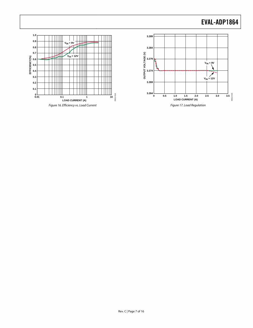
MEASURING EFFICIENCY AND LOAD REGULATION Using the voltages from the voltmeters and current readings from the source and load, calculate efficiency from the following equation:
ININ
OUTOUT
I V
I Vn
×
×=
Sweep the load across the full load range to obtain the efficiency and load regulation plot.
The efficiency results should correspond to the ADP1864 Buck Design Software.
MEASURING LINE REGULATION Vary the input voltage and examine the change in the output voltage reading from the voltmeter.
MONITORING SHORT-CIRCUIT BEHAVIOR Place a current probe on the load cable that connects the output to the positive input of the electronic load. Monitor the output voltage with a similar technique used to measure the output voltage ripple; however, dc couple the scope with a 5 V/div setting. Many electronic loads have short-circuit capability. Enable this function on the load and ensure that the circuit current limits at the correct current.
0561
2-01
7
Figure 3. Measuring Technique for Output Voltage Ripple
Figure 4. Switch Node Ringing at 3 A Load; VIN = 9 V 05
612-
003
C4 DC1M5.00V/div
–5.00V ofst
Timebase –1.19µsWStream12.5ks
500ns2.5GSPS
Trigger C4 DC
C4
AutoEdge
4.55VPositive
Figure 5. Switch Node Ringing at 3 A Load; VIN = 12 V
0561
2-00
4
Timebase 0.00µsWStream50.0ks
2.00ns2.5GSPS
Trigger C1 DCSingleEdge
–168mVPositive
C3 BWL AC1M50.0mV/div0.0mV ofst
C3
Figure 6. VOUT Ripple at 3 A Load; VIN = 9 V
0561
2-00
5
C3 BWL AC1M50.0mV/div0.0mV ofst
C3
TimebaseWStream50.0ks
–4.76µs2.00ns
2.5GSPS
TriggerAutoEdge
C4 DC4.55V
Positive
Figure 7. VOUT Ripple at 3 A Load; VIN = 12 V
0561
2-00
6
C4 DC1M5.00V/div
–5.00V ofst
TimebaseWStream12.5ks
–1.19µs500ns
2.5GSPS
TriggerStopEdge
C4 DC4.55V
Positive
C4
Figure 8. Gate Waveform 3 A; VIN = 9 V
0561
2-00
7
C4 DC1M5.00V/div
–5.00V ofst
TimebaseWStream25.0ks
–2.38µs1.00ns
2.5GSPS
TriggerStopEdge
C4 DC7.00V
Positive
C4
Figure 9. Gate Waveform 3 A; VIN = 12 V
EVAL-ADP1864
Rev. C | Page 6 of 16
0561
2-00
8
IOUT
VOUT
C3
IOUT
VOUT
C3
C2
TimebaseWStream1.00MS
–476µs200µs
500MSPS
TriggerAuto
C2 DC2.21A
Edge Positive 0561
2-01
1
C2 DC1.00A/div
0mA offset
C2 DC5.00A/div
–5.00A ofst
TimebaseWStream1.25MS
–119µs50.0µs
2.5GSPS
C3 DC1M5.00V/div
–10.00V ofst
C3 BWL AC1M100mV/div0.0mV ofst
TriggerStopEdge
C2 DC5.35A
Positive
Figure 10. Load Transient; 1.5 A to 3 A at 250 mA/μs, VIN = 9 V 05
612-
009
TimebaseWStream1.00MS
–476µs200µs
500MSPS
TriggerAuto
C2 DC2.21A
Edge Positive
C2 DC1.00A/div
0mA offset
C3 BWL AC1M100mV/div0.0mV ofst
IOUT
VOUT
C3
Figure 11. Load Transient; 1.5 A to 3 A at 250 mA/μs, VIN = 12 V
0561
2-01
0
TimebaseWStream1.25MS
–119µs50.0µs
2.5GSPS
TriggerStopEdge
C2 DC5.35A
Positive
C3 DC1M5.00V/div
–10.00V ofst
C2 DC5.00A/div
–5.00A ofst
IOUT
VOUT
C3
C2
Figure 12. Short Circuit; VIN = 9 V
Figure 13. Short Circuit; VIN = 12 V
IOUT
VOUT
COMP/EN
C3
C2
C4
C2 DC2.00A/div
2.860A ofst
0561
2-01
2
C3 DC1M1.00V/div
–2.030V ofst
C4 DC1M1.00V/div
0mV offset
TimebaseWStream1.25MS
–119µs50.0µs
2.5GSPS
TriggerStopEdge
C2 DC1.15V
Negative
Figure 14. Disable; VIN = 9 V
IOUT
VOUT
COMP/EN
C3
C2
C4
C2 DC2.00A/div
2.860A ofst
0561
2-01
3
TimebaseWStream1.25MS
–119µs50.0µs
2.5GSPS
C3 DC1M1.00V/div
–2.030V ofst
C4 DC1M1.00V/div
0mV offset
TriggerStopEdge
C3 DC1.15V
Negative
Figure 15. Disable; VIN = 12 V
EVAL-ADP1864
Rev. C | Page 7 of 16
1.0
0.9
0.8
0.7
0.6
0.5
0.4
0.3
0.2
EFFI
CIE
NC
Y(%
)
3.289
3.284
3.279
3.274
3.269
3.264
OU
TPU
T VO
LTA
GE
(V)
0.1
00.01 0.1 1 10
LOAD CURRENT (A) 0561
2-01
4
VIN = 12V
VIN = 9V
Figure 16. Efficiency vs. Load Current
VIN = 9V
VIN = 12V
0 0.5 1.0 1.5 2.0 2.5 3.0 3.5
612-
015
LOAD CURRENT (A) 05
Figure 17. Load Regulation
EVAL-ADP1864
Rev. C | Page 8 of 16
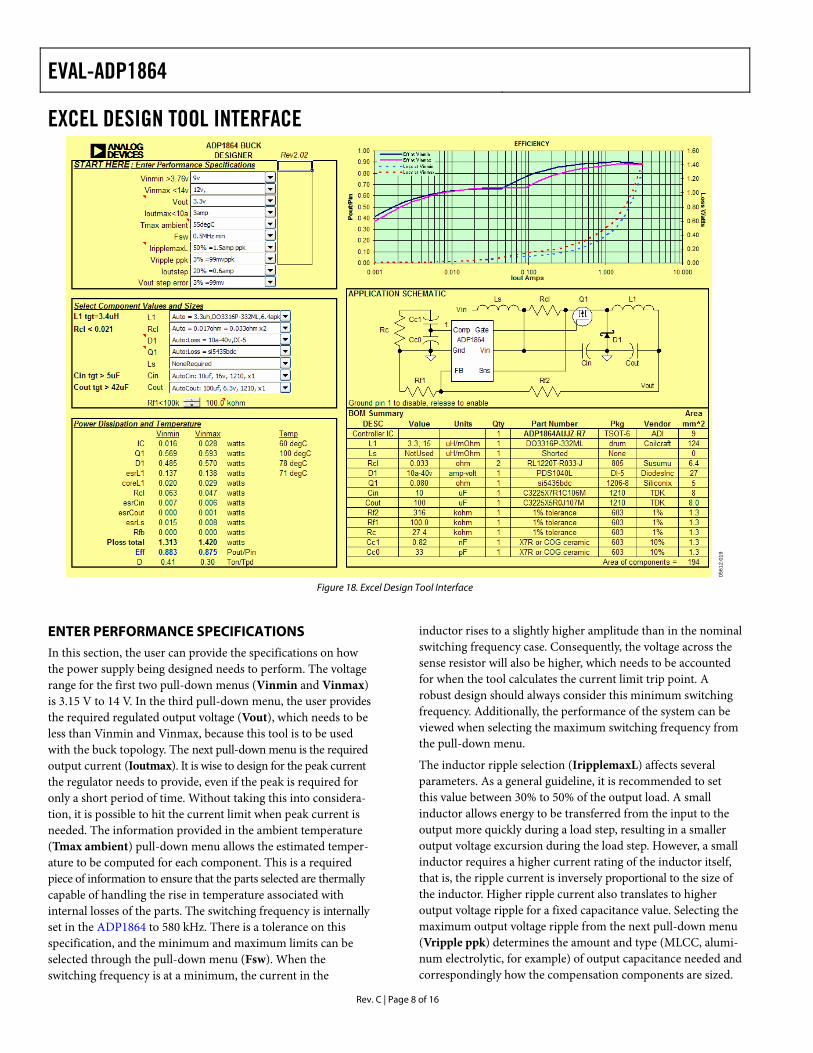
EXCEL DESIGN TOOL INTERFACE
0561
2-01
9
Figure 18. Excel Design Tool Interface
ENTER PERFORMANCE SPECIFICATIONS In this section, the user can provide the specifications on how the power supply being designed needs to perform. The voltage range for the first two pull-down menus (Vinmin and Vinmax) is 3.15 V to 14 V. In the third pull-down menu, the user provides the required regulated output voltage (Vout), which needs to be less than Vinmin and Vinmax, because this tool is to be used with the buck topology. The next pull-down menu is the required output current (Ioutmax). It is wise to design for the peak current the regulator needs to provide, even if the peak is required for only a short period of time. Without taking this into considera-tion, it is possible to hit the current limit when peak current is needed. The information provided in the ambient temperature (Tmax ambient) pull-down menu allows the estimated temper-ature to be computed for each component. This is a required piece of information to ensure that the parts selected are thermally capable of handling the rise in temperature associated with internal losses of the parts. The switching frequency is internally set in the ADP1864 to 580 kHz. There is a tolerance on this specification, and the minimum and maximum limits can be selected through the pull-down menu (Fsw). When the switching frequency is at a minimum, the current in the
inductor rises to a slightly higher amplitude than in the nominal switching frequency case. Consequently, the voltage across the sense resistor will also be higher, which needs to be accounted for when the tool calculates the current limit trip point. A robust design should always consider this minimum switching frequency. Additionally, the performance of the system can be viewed when selecting the maximum switching frequency from the pull-down menu.
The inductor ripple selection (IripplemaxL) affects several parameters. As a general guideline, it is recommended to set this value between 30% to 50% of the output load. A small inductor allows energy to be transferred from the input to the output more quickly during a load step, resulting in a smaller output voltage excursion during the load step. However, a small inductor requires a higher current rating of the inductor itself, that is, the ripple current is inversely proportional to the size of the inductor. Higher ripple current also translates to higher output voltage ripple for a fixed capacitance value. Selecting the maximum output voltage ripple from the next pull-down menu (Vripple ppk) determines the amount and type (MLCC, alumi-num electrolytic, for example) of output capacitance needed and correspondingly how the compensation components are sized.
As a general guideline, it is recommended to set this value around 5%. In the next pull-down menu (Ioutstep), the user can select the estimate of the largest step in load the regulator will demand. This, in conjunction with the allowable voltage excursion on load transient (in the Vout step error pull-down menu), delegates how much output capacitance is required. If the Ioutstep specification is not known, entering a 50% load step provides an adequate design for most applications at the power level the ADP1864 is designed to be used.
SELECT COMPONENT VALUES AND SIZES When starting a new design, it is recommended to reset each of the pull-down menus to Auto, which is at the top of the list for each option. With these settings, the tool automatically calculates the most efficient design and provides that solution. If the user would like to explore how other components affect various parameters of the system, all the parts of the regulator except the compensation components can be changed through the use of the pull-down menus in this section. Note that the tool provides a bill of materials that maintains all specifications entered in the Enter Performance Specifications section of the tool when a component is changed. Accordingly, other component values can change as well. The feedback resistor selector at the bottom of this section finds the right combination of resistors to provide the feedback voltage with the 0.8 V.
POWER DISSIPATION AND TEMPERATURE The Power Dissipation and Temperature section of the tool provides the user with the power dissipation of each part at the full rated current at both the maximum and minimum input voltages. It also provides the user with the estimated temperature of the ADP1864, the MOSFET, the diode, and the inductor. These calculations are done taking into account the temperature rise due to dissipation as well as the ambient temperature.
EFFICIENCY From the power dissipation information calculated in the Power Dissipation and Temperature section of the tool, the efficiency across the full load range is plotted for both maximum and minimum input voltages.
APPLICATION SCHEMATIC The Application Schematic section provides a schematic of the ADP1864 evaluation board. The reference designators on the evaluation board match this schematic.
BOM SUMMARY The BOM Summary provides the user with the final parts list necessary to meet all the requirements entered into the performance specifications section. Vendors, part numbers, individual and total area, along with a value for each component, are provided. If no part number is provided, a vital specification is given instead. This specification can be used to find a part to populate on the board. From this BOM, the user can modify the fully populated configuration or populate the bare board configuration to validate design changes.
MODIFYING THE EVALUATION BOARD The ADP1864-EVALZ evaluation board is complete and tested for operation. Due to the versatility of the ADP1864 step-down dc-to-dc controller, the ADP1864 evaluation board can be modified for a variety of external components. Some of the most common modifications are described in this section.
CHANGING THE MOSFET The ADP1864-EVALZ evaluation board is supplied with a Siliconix Si5435 power MOSFET. The layout can accommodate MOSFETs placed in parallel to accommodate higher current levels. Additionally, 8-lead SOIC, thermally enhanced 8-lead SOIC, 6-lead TSOP, 1206-8, and SOT-23 packages all have footprints available on the ADP1864 evaluation board. On resistances, gate charges and capacitances, gate-to-source thresholds, and maximum drain to source voltage ratings should all be considered before changing the MOSFET.
CHANGING THE SENSE RESISTOR If an increase in current capability is desired, it may be necessary to change the current limit via the sense resistor. As supplied, two 33 mΩ resistors in parallel are used to sense current. For duty cycles <40%, the current limit voltage is 125 mV typically. For duty cycles >40%, use the slope factor (SF) vs. duty cycle plot in the ADP1864 data sheet to determine the actual current sense limit.
Note that across the full temperature range and input voltage range of the ADP1864, the current limit voltage can be as low as 80 mV.
CHANGING THE DIODE The ADP1864-EVALZ evaluation board is supplied with a Diodes, Inc. PDS1040L Schottky diode. The board can accom-modate SMC, DPAK (TO-252), and other popular packages. The two primary factors to consider when changing the diode are the current handling capabilities as well as the maximum reverse dc blocking voltage. Because of switch node voltage excursions, it is recommended to select a diode with at least three times the reverse dc blocking voltage as the maximum input voltage for the application when no snubber circuit is used.
CHANGING THE OUTPUT INDUCTOR The ADP1864-EVALZ evaluation board is populated with a Coilcraft DO3316P-332ML 3.3 μH inductor with a saturation current of 6.4 A. To operate at currents higher than this, the inductor needs to be modified to accommodate at least the higher current plus half the inductor ripple current. If the current demand is less, it could be advantageous to select a physically smaller and lower saturation current inductor for cost consider-ations. Changing the inductance value can affect the stress on the transistor and diode, the output voltage ripple, and the load transient response. The ADP1864 Buck Design Software accounts
for all these changes when the new inductance value is selected from the L1 pull-down menu. It then provides new suggestions for component values. The Applications Information section of ADP1864 data sheet also provides information concerning the implications of changing the output inductor. If the duty cycle is to exceed 40%, keep the ripple current to 30% to 50% of the output current so that the slope compensation remains effective. See the ADP1864 data sheet for more details.
CHANGING THE OUTPUT CAPACITORS The ADP1864-EVALZ evaluation board is supplied with a 100 μF ceramic capacitor on the output. If the capacitance is insufficient to meet load transient requirements, a D-case tantalum capacitor footprint and an 8 mm electrolytic capacitor footprint are available to provide the capability to greatly increase the output capacitance. Any change in output capacitance also requires a change in compensation component values. To compensate for a change in output capacitor, use the following equations:
REFLOADM
CCLOUTLOADOUTUNC VRG
GRVRESRCfR
××
×××+×××=
2
2)(2π
UNCC1 fR
C××
=π2
3
OUTCCLLOADUN
REFLOADMC0 VGRRESRf
VESRRGC
×××+××××× or =
)(2π
SWCC0 fR
C××
=π2
3 , whichever is larger.
where: fUN is the desired unity gain frequency in hertz (usually 40 kHz). COUT is output capacitance in farads. ESR is the effective series resistance of COUT in ohms. RLOAD is VOUT (volts)/maximum load current (amps). RCL is the parallel resistance of the current sense resistors in ohms. GC is the nominal gain of the current sense amplifier (12). GM is the nominal gain of the error amplifier (2.4 × 10⁻⁴ mhos). VREF is the nominal error amplifier reference voltage (0.8 V). fSW is the nominal switching frequency of the ADP1864 (580 kHz).
If multiple output capacitors are used and of the same type and value, ESR is defined as the parallel effective series resistance of all the capacitors. If multiple output capacitors are used that are not of the same type and value, the analysis to calculate optimal compensation components is considerably more complicated and beyond the scope of this document.
It is recommended to always refer to the manufacturer’s data for capacitance derating over applied voltage and temperature.
CHANGING THE OUTPUT VOLTAGE The ADP1864-EVALZ evaluation board output regulation voltage can be changed by altering the voltage divider consisting of RF2 and RF1. The output regulation voltage is determined by the following equation:
⎟⎟⎠
⎞⎜⎜⎝
⎛ +×=
1
128.0F
FFOUT R
RRV
Modifying the output voltage changes the inductor ripple current and subsequently the output voltage ripple, transient response, and stress on the PFET. The design tool considers this and, if necessary, provides new component values.