EVAL-ADAU1467Z UG-1134 One Technology Way • P.O. Box 9106 • Norwood, MA 02062-9106, U.S.A. • Tel: 781.329.4700 • Fax: 781.461.3113 • www.analog.com Evaluating the ADAU1463 and ADAU1467 SigmaDSP Audio Processors PLEASE SEE THE LAST PAGE FOR AN IMPORTANT WARNING AND LEGAL TERMS AND CONDITIONS. Rev. 0 | Page 1 of 57 FEATURES 4 analog inputs 8 analog outputs Stereo S/PDIF input and output Self boot EEPROM Headers for interfacing to off board peripherals EVALUATION KIT CONTENTS EVAL-ADAU1467Z evaluation board EVAL-ADUSB2EBZ (USBi) communications adapter USB cable with Mini-B plug 6 V ac to dc power supply HARDWARE REQUIRED PC running Windows XP, Windows Vista, or Windows 7 Analog, stereo audio source with an output cable terminated with a 3.5 mm (1/8 inch) plug (for the analog input) Headphones, desktop speakers, or audio input with a cable terminated with a 3.5 mm (1/8 inch) plug (for the analog output) S/PDIF audio source and receiver, each with optical cables terminated with TOSLINK connectors (for digital input/output) SOFTWARE REQUIRED SigmaStudio software, available for download from the SigmaStudio product page DOCUMENTS NEEDED ADAU1467 data sheet AD1937 data sheet AN-1006 Application Note GENERAL DESCRIPTION This user guide details the design, setup, and operation of the EVAL-ADAU1467Z evaluation board. This board is suitable for the evaluation of, and software development for, the ADAU1467 and ADAU1463 SigmaDSP® processors. Note that the ADAU1467 and the ADAU1463 are functionally identical; however, the ADAU1467 has more program and data memory than the ADAU1463. When using this evaluation board to evaluate the ADAU1463, select the ADAU1463 block (see the Setting Up Communications in SigmaStudio section) rather than the ADAU1467, as shown in Figure 16. Performing this action informs the compiler to limit the amount of memory allocated to match the ADAU1463. All other procedures and instructions in this user guide are identical for the ADAU1463 and ADAU1467. This evaluation board provides access to the digital serial audio ports of the ADAU1467. Four analog inputs and eight analog outputs are provided by the AD1937 codec included in the evaluation kit. Switches enable the evaluation of alternate features provided by many of the pins with multiplexed functionality, and numerous headers provide access to serial audio ports and the master and slave control ports. These selectable modes and headers make the EVAL-ADAU1467Z well suited to prototyping larger application circuits, as well as initial device evaluation. The ADAU1467 core is programmed using Analog Devices, Inc., SigmaStudio® software, which interfaces to the evaluation board via a USB interface (USBi). The on-board, electronically erasable programmable read only memory (EEPROM) can be programmed for self boot mode. The evaluation board is powered by a 6 V dc supply, which is regulated to the voltages required on the board. The printed circuit board (PCB) is a 4-layer design with a ground plane and a power plane on the inner layers. The evaluation board includes connectors for external analog inputs and outputs and optical Sony/Philips Digital Interface (S/PDIF) interfaces. The master clock is provided by the integrated oscillator circuit and the on- board 12.288 MHz passive crystal. For full details, see the ADAU1467 and AD1937 data sheets, which must be used in conjunction with this user guide when using the evaluation board.
Transcript
EVAL-ADAU1467ZUG-1134
One Technology Way • P.O. Box 9106 • Norwood, MA 02062-9106, U.S.A. • Tel: 781.329.4700 • Fax: 781.461.3113 • www.analog.com
Evaluating the ADAU1463 and ADAU1467 SigmaDSP Audio Processors
PLEASE SEE THE LAST PAGE FOR AN IMPORTANT WARNING AND LEGAL TERMS AND CONDITIONS. Rev. 0 | Page 1 of 57
FEATURES 4 analog inputs 8 analog outputs Stereo S/PDIF input and output Self boot EEPROM Headers for interfacing to off board peripherals
EVALUATION KIT CONTENTS EVAL-ADAU1467Z evaluation board EVAL-ADUSB2EBZ (USBi) communications adapter USB cable with Mini-B plug 6 V ac to dc power supply
HARDWARE REQUIRED PC running Windows XP, Windows Vista, or Windows 7 Analog, stereo audio source with an output cable terminated
with a 3.5 mm (1/8 inch) plug (for the analog input) Headphones, desktop speakers, or audio input with a cable
terminated with a 3.5 mm (1/8 inch) plug (for the analog output)
S/PDIF audio source and receiver, each with optical cables terminated with TOSLINK connectors (for digital input/output)
SOFTWARE REQUIRED SigmaStudio software, available for download from the
SigmaStudio product page
DOCUMENTS NEEDED ADAU1467 data sheet AD1937 data sheet AN-1006 Application Note
GENERAL DESCRIPTION This user guide details the design, setup, and operation of the EVAL-ADAU1467Z evaluation board. This board is suitable for the evaluation of, and software development for, the ADAU1467 and ADAU1463 SigmaDSP® processors. Note that the ADAU1467 and the ADAU1463 are functionally identical; however, the ADAU1467 has more program and data memory than the ADAU1463. When using this evaluation board to evaluate the ADAU1463, select the ADAU1463 block (see the Setting Up Communications in SigmaStudio section) rather than the ADAU1467, as shown in Figure 16. Performing this action informs the compiler to limit the amount of memory allocated to match the ADAU1463. All other procedures and instructions in this user guide are identical for the ADAU1463 and ADAU1467.
This evaluation board provides access to the digital serial audio ports of the ADAU1467. Four analog inputs and eight analog outputs are provided by the AD1937 codec included in the evaluation kit. Switches enable the evaluation of alternate features provided by many of the pins with multiplexed functionality, and numerous headers provide access to serial audio ports and the master and slave control ports. These selectable modes and headers make the EVAL-ADAU1467Z well suited to prototyping larger application circuits, as well as initial device evaluation. The ADAU1467 core is programmed using Analog Devices, Inc., SigmaStudio® software, which interfaces to the evaluation board via a USB interface (USBi). The on-board, electronically erasable programmable read only memory (EEPROM) can be programmed for self boot mode. The evaluation board is powered by a 6 V dc supply, which is regulated to the voltages required on the board. The printed circuit board (PCB) is a 4-layer design with a ground plane and a power plane on the inner layers. The evaluation board includes connectors for external analog inputs and outputs and optical Sony/Philips Digital Interface (S/PDIF) interfaces. The master clock is provided by the integrated oscillator circuit and the on-board 12.288 MHz passive crystal.
For full details, see the ADAU1467 and AD1937 data sheets, which must be used in conjunction with this user guide when using the evaluation board.
SETTING UP THE EVALUATION BOARD Using the EVAL-ADAU1467Z evaluation board requires a PC running Windows® XP or later with a USB interface and an internet connection. The PC communicates with the evaluation board using the included USBi interface. The software tool chain used with the ADAU1467 is SigmaStudio, a fully graphical user interface (GUI)-based programming environment. No DSP programming is required. A full version of SigmaStudio, which includes a library of DSP building blocks and the required USBi drivers, is available for download from the SigmaStudio software page on the Analog Devices website at www.analog.com/SigmaStudio.
INSTALLING THE SigmaStudio SOFTWARE To download the latest version of SigmaStudio, take the following steps:
1. Go to the SigmaStudio software page on the Analog Devices website, and select the latest version of the SigmaStudio software from the Downloads and Related Software section.
2. Determine whether the software must be installed on a 32-bit or 64-bit version of Windows, and locate the latest release version of SigmaStudio as appropriate.
3. Download the installer and execute the executable. Follow the prompts, and accept the license agreement to install the software.
INSTALLING THE USBi (EVAL-ADUSB2EBZ) DRIVERS SigmaStudio must be installed to use the USB interface (USBi). After the SigmaStudio installation is complete, take the following steps:
1. Connect the USBi to an available USB 2.0 port using the USB cable included in the evaluation board kit. Note that the USBi does not function properly with a USB 3.0 port.
2. Install the driver software (see the Using Windows XP section or the Using Windows 7 or Windows Vista section for more information).
Using Windows XP
1578
6-00
2
Figure 2. Found New Hardware Notification
After connecting the USBi to the USB 2.0 port, Windows recognizes the device (see Figure 2) and prompts the user to install the drivers. To install these drivers, take the following steps:
1. From the Found New Hardware Wizard window, select the installation from a list or from a specific location using the advanced option, and click Next (see Figure 3).
1578
6-00
3
Figure 3. Found New Hardware Wizard Installation
2. Click Search for the best driver in these locations, select Include this location in the search, and click Browse to find the USB drivers subdirectory within the SigmaStudio directory (see Figure 4).
1578
6-00
4
Figure 4. Found New Hardware Wizard—Search and Installation Options
3. When the warning about Windows logo testing appears, click Continue Anyway (see Figure 5).
1578
6-00
5
Figure 5. Hardware Installation—Windows Logo Testing Warning
The USBi drivers are now installed. Leave the USBi connected to the PC.
Using Windows 7 or Windows Vista
After connecting the USBi to the USB 2.0 port, Windows 7 or Windows Vista recognizes the device and installs the drivers automatically (see Figure 6). After the installation is complete, leave the USBi connected to the PC.
1578
6-00
6
Figure 6. USBi Driver Installed Correctly
Confirming Proper Installation of the USBi Drivers
To confirm that the USBi drivers are installed properly, take the following steps:
1. With the USBi still connected to the USB 2.0 port of the computer, check that both the yellow I2C LED and the red power indicator LED are illuminated (see Figure 7).
1578
6-00
7
Figure 7. State of the USBi Status LEDs After Driver Installation
2. In the Windows Device Manager, under the Universal Serial Bus controllers section, check that Analog Devices USBi (programmed) is displayed (see Figure 8).
1578
6-00
8
Figure 8. Confirming Driver Installation Using the Device Manager
DISABLING THE SELF BOOT SWITCH When setting up the EVAL-ADAU1467Z evaluation board, ensure that the SELFBOOT switch is in the off position. SELFBOOT is the first switch of the four position, dual inline package (DIP) switches, S3. The off position is toward the bottom of the board, away from the silkscreen label, SELFBOOT.
The default position of this switch is the off (disabled) position, which prevents the ADAU1467 from executing a self boot operation at power-up. When the switch is in the on position, the LED D3 is illuminated, and a self boot operation is executed, causing the ADAU1467 to attempt to load code from the EEPROM (U10) when it powers up or comes out of reset.
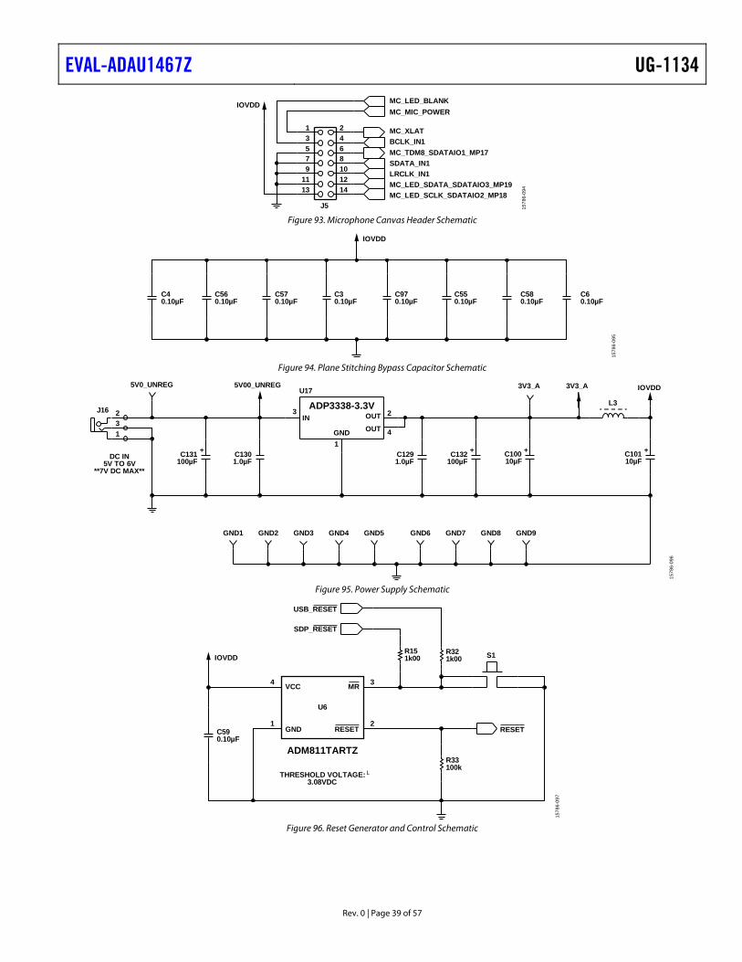
POWERING UP THE EVALUATION BOARD Power is supplied to the evaluation board using a dc power supply with a female positive center plug. The plug has a 2.1 mm inner diameter, a 5.5 mm outer diameter, and a 9.5 mm length (see Figure 9). The output must range between 5 V and 7 V and must be able to source at least 1.5 A of current. Connect the power supply to Connector J4. The unregulated supply powers the operational amplifiers used in the active audio filters for the analog audio inputs and outputs. An on-board linear regulator (U17) generates the 3.3 V dc supply required for the ADAU1467 and AD1937, as well as other supporting ICs. When the power supply is connected properly, LED D9 illuminates.
1578
6-00
9
Figure 9. DC Power Supply Plug and Cable
To power up the evaluation board, take the following steps:
1. Connect the included power supply to the wall outlet (100 V to 240 V, ac 50 Hz to 60 Hz).
2. Connect the female plug of the power supply to the J4 male connector on the EVAL-ADAU1467Z, as shown in Figure 10.
1578
6-01
0
Figure 10. Connecting the Power Supply
3. After the power supply is connected, the D2 status LED (A_3V3) illuminates.
4. Connect the ribbon cable of the USBi to the control port of the EVAL-ADAU1467Z (see Figure 11). The USBi must already be connected to the USB 2.0 port of the computer.
1578
6-01
1
Figure 11. Connecting the USBi to the Serial Peripheral Interface (SPI)
CONNECTING THE AUDIO CABLES To connect the audio cables to the evaluation board, take the following steps:
1. Connect a stereo audio source to J14 (IN1) with a standard 3.5 mm (1/8 inch) stereo tip, ring, sleeve (TRS) audio cable. The audio signals must be single-ended and line level, with a maximum voltage of 2.8 V p-p. The tip of the plug is the left channel of audio, the ring is the right channel of audio, and the sleeve is the common or ground.
2. Connect headphones or powered speakers to J12 (OUT1).
Figure 12 shows the input source connection. Figure 13 shows the output connection. Figure 14 shows the location of the connectors on the board.
SETTING UP COMMUNICATIONS IN SigmaStudio To set up communications in SigmaStudio, take the following steps:
1. Start the SigmaStudio software by double clicking the shortcut on the desktop or by finding and executing the executable file in Windows Explorer.
2. To create a new project, select New Project from the File menu or press CTRL + N. (The default view of the new project is the Hardware Configuration tab.)
3. In the Hardware Configuration tab, add the appropriate components to the project space by clicking and dragging them from the Tree ToolBox on the left of the window to the empty white space located on the right of the window. a. Click USBi to add a USBi component from the
Communication Channels subsection of the toolbox (see Figure 15).
1578
6-01
5
Figure 15. Adding the USBi Communication Channel
b. Add an ADAU1467 component from the Processors (ICs/DSPs) subsection of the toolbox (see Figure 16).
1578
6-01
6
Figure 16. Adding an ADAU1467
4. Ensure that SigmaStudio can detect the USBi on the USB port of the PC as follows: a. When SigmaStudio detects the USBi, the background
of the USB label is green in the USB Interface box (see Figure 17).
1578
6-01
7
Figure 17. USBi Detected by SigmaStudio
b. When SigmaStudio cannot detect the USBi on the USB port of the PC, the background of the USB label is red (see Figure 18). This error can occur when the USBi is not connected or when the drivers are installed incorrectly.
1578
6-01
8
Figure 18. USBi Not Detected by SigmaStudio
c. To connect the USBi block (USB interface) to the target integrated circuit (IC) block of the ADAU1467, click and drag a line, representing a wire, between the blue pin of the USBi and the green pin of the IC (see Figure 19). This connection allows the USBi to comm-unicate with the ADAU1467. The corresponding dropdown box of the USBi automatically fills with the default mode and channel for that IC. In the case of the ADAU1467, the default communications mode is SPI, the default slave select line is 1, and the default address is 0.
1578
6-01
9
Figure 19. Connecting the USBi to an ADAU1467 in the Hardware
CREATING A BASIC SIGNAL FLOW To create a signal processing flow, take the following steps:
1. Click the Schematic tab near the top of the window (see Figure 20).
1578
6-02
0
Figure 20. Schematic Tab
2. To add the appropriate elements to the project space, click and drag the elements from the Tree ToolBox on the left of the window to the empty white space located on the right of the window. The toolbox contains all of the algorithms that can run in SigmaDSP. a. To add an Input block, from the (IC1) ADAU1467 >
IO > Input > sdata 32-39 folder, click Input (see Figure 21) and drag it into the project space to the right of the toolbox (see Figure 22). By default, Channel 0 and Channel 1 are selected. This configuration matches the analog audio source hardware connections shown in Figure 12 and Figure 13; therefore, no modifications are required.
1578
6-02
1
Figure 21. Input Block Selection
1578
6-02
2
Figure 22. Input Block
b. Add two Output blocks as follows, ensuring that these blocks are assigned to Channel 0 and Channel 1: i. From the (IC1) ADAU1467 > IO > Output folder,
click Output (see Figure 23) and drag it into the project space to the right of the toolbox.
1578
6-02
3
Figure 23. Output Block Selection
ii. Repeat the previous step to add another output (see Figure 24).
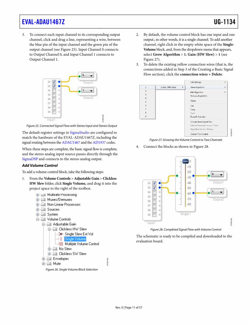
3. To connect each input channel to its corresponding output channel, click and drag a line, representing a wire, between the blue pin of the input channel and the green pin of the output channel (see Figure 25). Input Channel 0 connects to Output Channel 0, and Input Channel 1 connects to Output Channel 1.
1578
6-02
5
Figure 25. Connected Signal Flow with Stereo Input and Stereo Output
The default register settings in SigmaStudio are configured to match the hardware of the EVAL-ADAU1467Z, including the signal routing between the ADAU1467 and the AD1937 codec.
When these steps are complete, the basic signal flow is complete, and the stereo analog input source passes directly through the SigmaDSP and connects to the stereo analog output.
Add Volume Control
To add a volume control block, take the following steps:
1. From the Volume Controls > Adjustable Gain > Clickless HW Slew folder, click Single Volume, and drag it into the project space to the right of the toolbox.
1578
6-02
6
Figure 26. Single Volume Block Selection
2. By default, the volume control block has one input and one output.; in other words, it is a single channel. To add another channel, right click in the empty white space of the Single-Volume block, and, from the dropdown menu that appears, select Grow Algorithm > 1. Gain (HW Slew) > 1 (see Figure 27).
3. To delete the existing yellow connection wires (that is, the connections added in Step 3 of the Creating a Basic Signal Flow section), click the connection wires + Delete.
1578
6-02
7
Figure 27. Growing the Volume Control to Two Channels
4. Connect the blocks as shown in Figure 28.
1578
6-02
8
Figure 28. Completed Signal Flow with Volume Control
The schematic is ready to be compiled and downloaded to the evaluation board.
DOWNLOADING THE PROGRAM TO THE DSP To compile and download the code to the digital signal processor (DSP), click the Link/Compile/Download button in the main toolbar of SigmaStudio (see Figure 29). Alternatively, press F7.
1578
6-02
9
Figure 29. Link/Compile/Download Button
After the code downloads to the DSP, the following events occur in order:
1. If the compiler completes compiling the project, the compiled data downloads from SigmaStudio via the USBi to the ADAU1467, and the SigmaDSP starts running.
2. The status bar turns from blue to green, and the mode displayed changes from Design Mode to Active: Downloaded in the lower right corner of the window (see Figure 30 and Figure 31). Until this point, SigmaStudio is in design mode, as denoted by the blue bar at the bottom of the screen and the words Design Mode displayed in the lower right corner of the SigmaStudio window (see Figure 30).
1578
6-03
0
Figure 30. Design Mode and Blue Status Bar
1578
6-03
1
Figure 31. Active Downloaded Mode and Green Status Bar
The signal flow runs on the evaluation board, and the audio passes from the analog input to the analog output. To change the volume in real time, click and drag the volume control slider in the Schematic tab.
If the Output window is open at the time of compilation, a compiler output log displays, as shown in Figure 32. The Output window can be opened or closed by using the keyboard shortcut CTRL + 4. The Output window shows the compiler output log only if it is open when the Link/Compile/Download button is clicked.
1578
6-03
2
Figure 32. Compiler Output Window
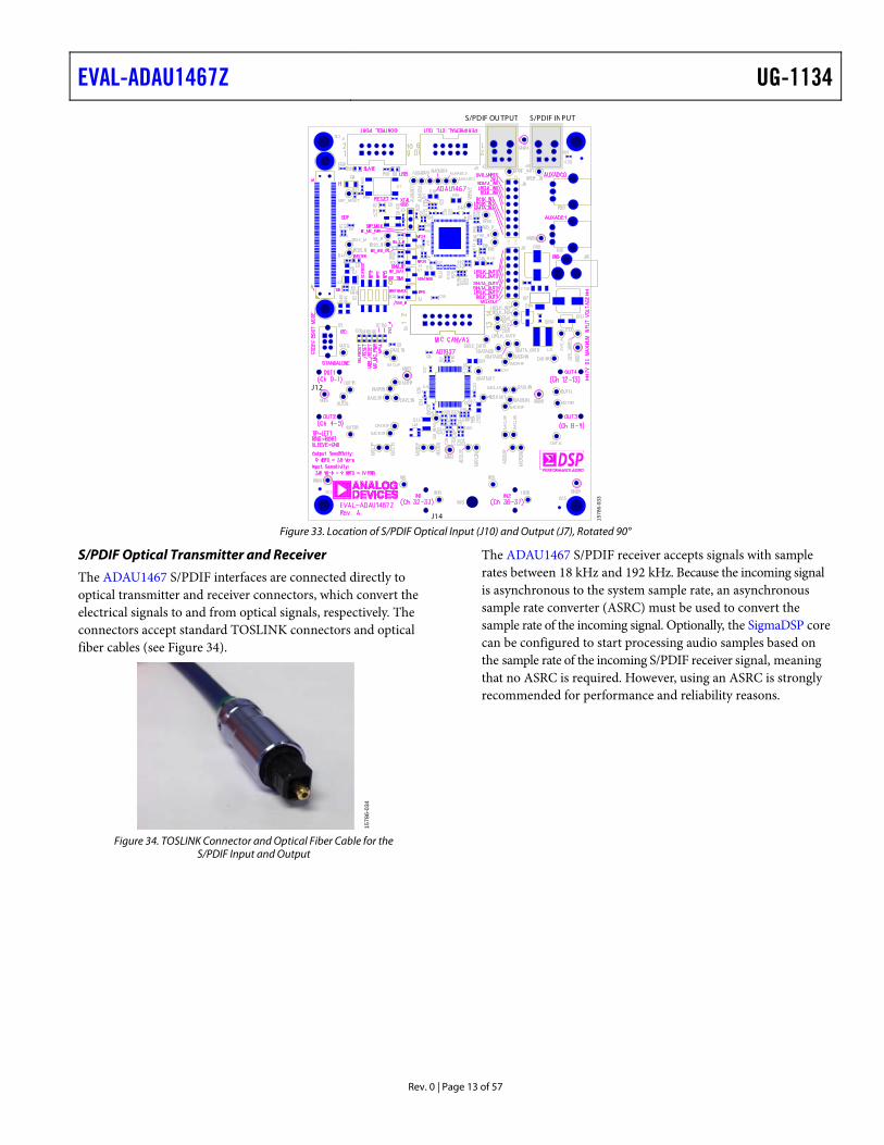
ADDING THE S/PDIF INPUT AND OUTPUT TO THE PROJECT The EVAL-ADAU1467Z evaluation board has two optical S/PDIF interfaces. One interface is an input that converts the optical signal to an electrical signal, which is sent to the ADAU1467 S/PDIF receiver (the SPDIFIN pin). The other interface is an optical output that takes the electrical output from the ADAU1467 S/PDIF transmitter (the SPDIFOUT pin) and converts it to an optical signal. Figure 33 shows the locations of the optical input connector and the optical output connector. The connectors are located on the underside of the PCB.
Figure 33. Location of S/PDIF Optical Input (J10) and Output (J7), Rotated 90°
S/PDIF Optical Transmitter and Receiver
The ADAU1467 S/PDIF interfaces are connected directly to optical transmitter and receiver connectors, which convert the electrical signals to and from optical signals, respectively. The connectors accept standard TOSLINK connectors and optical fiber cables (see Figure 34).
1578
6-03
4
Figure 34. TOSLINK Connector and Optical Fiber Cable for the
S/PDIF Input and Output
The ADAU1467 S/PDIF receiver accepts signals with sample rates between 18 kHz and 192 kHz. Because the incoming signal is asynchronous to the system sample rate, an asynchronous sample rate converter (ASRC) must be used to convert the sample rate of the incoming signal. Optionally, the SigmaDSP core can be configured to start processing audio samples based on the sample rate of the incoming S/PDIF receiver signal, meaning that no ASRC is required. However, using an ASRC is strongly recommended for performance and reliability reasons.
The ADAU1467 S/PDIF transmitter typically transmits signals from the DSP core, meaning that the sample rate of the audio coming out of the S/PDIF transmitter on the EVAL-ADAU1467Z is typically 44.1 kHz or 48 kHz. Optionally, the S/PDIF transmitter can be configured in a pass through mode, where it simply transmits a copy of the signal directly from the receiver.
Both the S/PDIF receiver and transmitter carry two channels of uncompressed audio.
To add an S/PDIF input and output to the project in SigmaStudio, take the following steps:
1. Connect an S/PDIF source to the EVAL-ADAU1467Z evaluation board by using a standard TOSLINK optical cable and connecting it to the S/PDIF receiver connector, U2 (see Figure 35).
1578
6-03
5
Figure 35. Photograph of the Optical S/PDIF Input Connection
2. Configure the S/PDIF input and output by modifying the ADAU1467 registers as follows: a. Click the Hardware Configuration tab, then click the
IC 1 - ADAU1467 Register Controls tab at the bottom of the window (see Figure 36).
1578
6-03
6
Figure 36. IC 1 – ADAU1467 Register Controls Tab
b. To access the SPDIF tab, click the right arrow to scroll (see Figure 37).Then, click the SPDIF tab (see Figure 38). There are several register control tabs listed across the top of the window.
1578
6-03
7
Figure 37. Using the Register Tab Scroll Button
1578
9-03
8
Figure 38. Selecting the SPDIF Tab
c. Enable the SPDIF_RESTART register by clicking Do not restart the audio once a re-lock has occurred in the SPDIF RESTART box. When this button is clicked, the text displayed on the button changes to Restarts the audio once a re-lock has occurred and the button color changes from red to green (see Figure 39).
1578
6-03
9
Figure 39. Activating the SPDIF_RESTART Register
d. To activate the S/PDIF interface, click the Disabled button in the SPDIF TX EN box. When this button is clicked, the text displayed on the button changes to Enabled and the button color changes from red to green (see Figure 40).
1578
6-04
0
Figure 40. Activating the SPDIF_TX_EN Register
e. To enable the S/PDIF receiver to operate at a sample rate up to 192 kHz, click SYSCLKDIV2 in the SPDIF RX MCLKSPEED box. When this button is clicked, the text changes to SYSCLK and the button color changes from green to red in the SPDIF TX MCLKSPEED box. To enable the S/PDIF transmitter to operate at a sample rate up to 192 kHz, click SYSCLKDIV2 in the SPDIF RX MCLKSPEED box. When this button is clicked, the text changes to SYSCLK and the button color changes from green to red in the SPDIF TX MCLKSPEED box (see Figure 41).
1578
6-04
1
Figure 41. Setting the Maximum Sample Rate of the S/PDIF Receiver and
Transmitter
3. Click the ROUTING_MATRIX tab (see Figure 42) to allow the configuration of the routing matrix.
4. To configure the S/PDIF receiver signal routing, click the first asynchronous sample rate converter, ASRC 0 (see Figure 43) and configure ASRC 0 using the dropdown menus until it matches what is shown in Figure 44. This configuration routes the S/PDIF receiver signal through an ASRC before it is accessed in the DSP core. Routing the signal in this way is necessary because the clock recovered from the S/PDIF source is not synchronous to the ADAU1467.
1578
6-04
3
Figure 43. ASRC 0 Control Button
1578
6-04
4
Figure 44. Configuring the ASRC 0 Routing Matrix Registers
5. Configure the S/PDIF transmitter (Tx) signal routing as follows: a. Click the S/PDIF TX box (see Figure 45).
1578
6-04
5
Figure 45. Configuring the S/PDIF Transmitter Routing Matrix Register
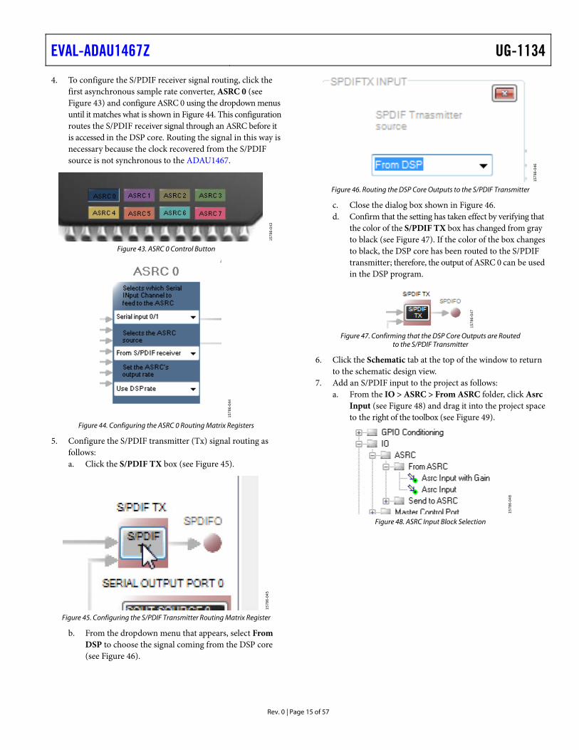
b. From the dropdown menu that appears, select From DSP to choose the signal coming from the DSP core (see Figure 46).
1578
6-04
6
Figure 46. Routing the DSP Core Outputs to the S/PDIF Transmitter
c. Close the dialog box shown in Figure 46. d. Confirm that the setting has taken effect by verifying that
the color of the S/PDIF TX box has changed from gray to black (see Figure 47). If the color of the box changes to black, the DSP core has been routed to the S/PDIF transmitter; therefore, the output of ASRC 0 can be used in the DSP program.
1578
6-04
7
Figure 47. Confirming that the DSP Core Outputs are Routed
to the S/PDIF Transmitter
6. Click the Schematic tab at the top of the window to return to the schematic design view.
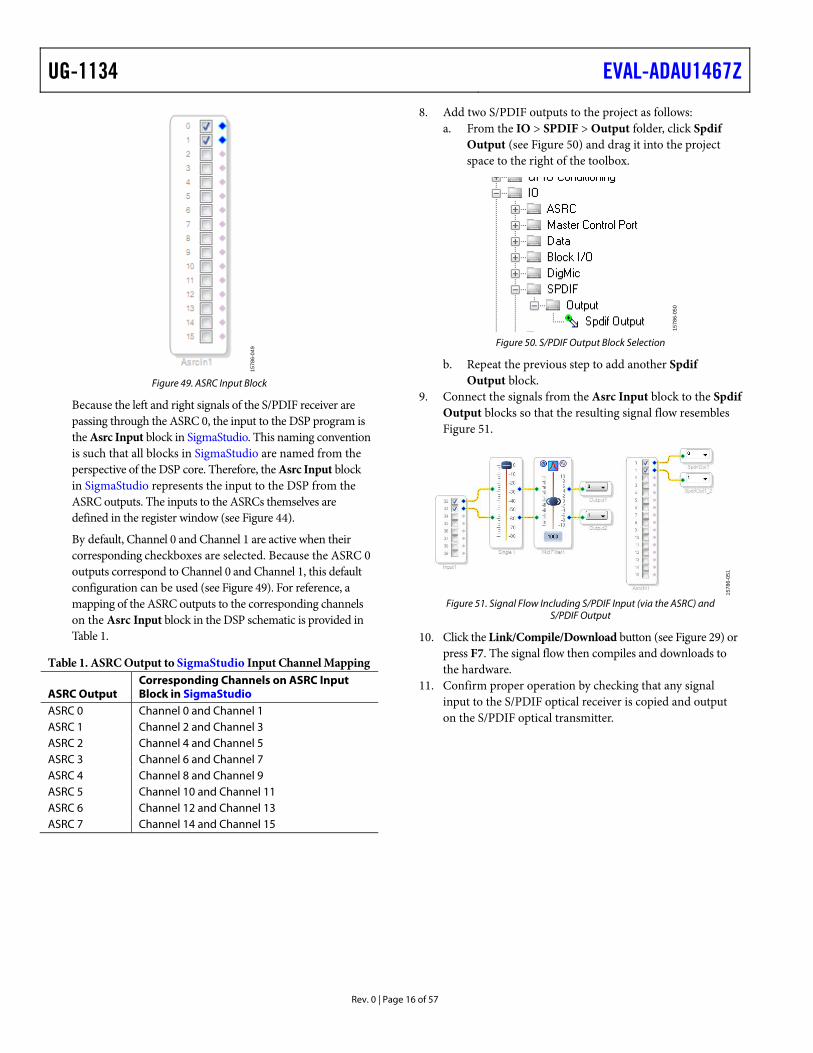
7. Add an S/PDIF input to the project as follows: a. From the IO > ASRC > From ASRC folder, click Asrc
Input (see Figure 48) and drag it into the project space to the right of the toolbox (see Figure 49).
Because the left and right signals of the S/PDIF receiver are passing through the ASRC 0, the input to the DSP program is the Asrc Input block in SigmaStudio. This naming convention is such that all blocks in SigmaStudio are named from the perspective of the DSP core. Therefore, the Asrc Input block in SigmaStudio represents the input to the DSP from the ASRC outputs. The inputs to the ASRCs themselves are defined in the register window (see Figure 44).
By default, Channel 0 and Channel 1 are active when their corresponding checkboxes are selected. Because the ASRC 0 outputs correspond to Channel 0 and Channel 1, this default configuration can be used (see Figure 49). For reference, a mapping of the ASRC outputs to the corresponding channels on the Asrc Input block in the DSP schematic is provided in Table 1.
Table 1. ASRC Output to SigmaStudio Input Channel Mapping
ASRC Output Corresponding Channels on ASRC Input Block in SigmaStudio
ASRC 0 Channel 0 and Channel 1 ASRC 1 Channel 2 and Channel 3 ASRC 2 Channel 4 and Channel 5 ASRC 3 Channel 6 and Channel 7 ASRC 4 Channel 8 and Channel 9 ASRC 5 Channel 10 and Channel 11 ASRC 6 Channel 12 and Channel 13 ASRC 7 Channel 14 and Channel 15
8. Add two S/PDIF outputs to the project as follows: a. From the IO > SPDIF > Output folder, click Spdif
Output (see Figure 50) and drag it into the project space to the right of the toolbox.
1578
6-05
0
Figure 50. S/PDIF Output Block Selection
b. Repeat the previous step to add another Spdif Output block.
9. Connect the signals from the Asrc Input block to the Spdif Output blocks so that the resulting signal flow resembles Figure 51.
1578
6-05
1
Figure 51. Signal Flow Including S/PDIF Input (via the ASRC) and
S/PDIF Output
10. Click the Link/Compile/Download button (see Figure 29) or press F7. The signal flow then compiles and downloads to the hardware.
11. Confirm proper operation by checking that any signal input to the S/PDIF optical receiver is copied and output on the S/PDIF optical transmitter.
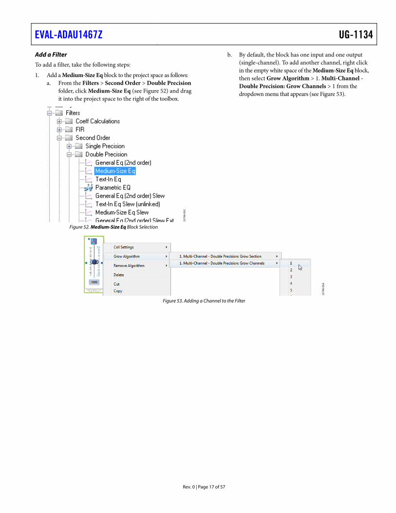
1. Add a Medium-Size Eq block to the project space as follows: a. From the Filters > Second Order > Double Precision
folder, click Medium-Size Eq (see Figure 52) and drag it into the project space to the right of the toolbox.
1578
6-05
2
Figure 52. Medium-Size Eq Block Selection
b. By default, the block has one input and one output (single-channel). To add another channel, right click in the empty white space of the Medium-Size Eq block, then select Grow Algorithm > 1. Multi-Channel - Double Precision: Grow Channels > 1 from the dropdown menu that appears (see Figure 53).
2. Connect the filter in series between the Asrc Input block and the Spdif Output blocks so that the filter can be applied to the signals passing through the DSP. The completed signal flow resembles Figure 54.
1578
6-05
5
Figure 54. Completed Signal Flow
3. Click the Link/Compile/Download button (see Figure 29) or press F7 to compile the signal flow and download it to the hardware. The audio signal passes from the S/PDIF receiver through the ASRCs into the DSP and the EQ filter, and then out on the S/PDIF transmitter. To change the settings of the EQ filter, click the blue icon at top of the block. To change the filter gain in real time while the project is running, drag the control slider in SigmaStudio.
CONTROLLING VOLUME WITH A POTENTIOMETER The 10-bit auxiliary analog-to-digital converter (ADC) on the ADAU1467 eliminates the need for a microcontroller in many applications by using analog control signals as user interface devices. For example, the EVAL-ADAU1467Z includes two 10 kΩ linear potentiometers connected to Auxiliary ADC Channel 0 (AUXADC0) and Auxiliary ADC Channel 1 (AUXADC1). These potentiometers can be used as an inexpensive, versatile, and physical way to control parameters such as gain, filter corner frequency, slew rate, and compression level.
1578
6-05
6
Figure 55. Potentiometers Connected to AUXADC0 and AUXADC1
The following example procedure demonstrates how a potentiometer can be configured as a stereo volume control.
1. Create a new project in SigmaStudio, and use the Hardware Configuration tab to set up the ADAU1467 as described in the Setting Up Communications in SigmaStudio section.
2. Add an input and two output blocks as described in the Creating a Basic Signal Flow section.
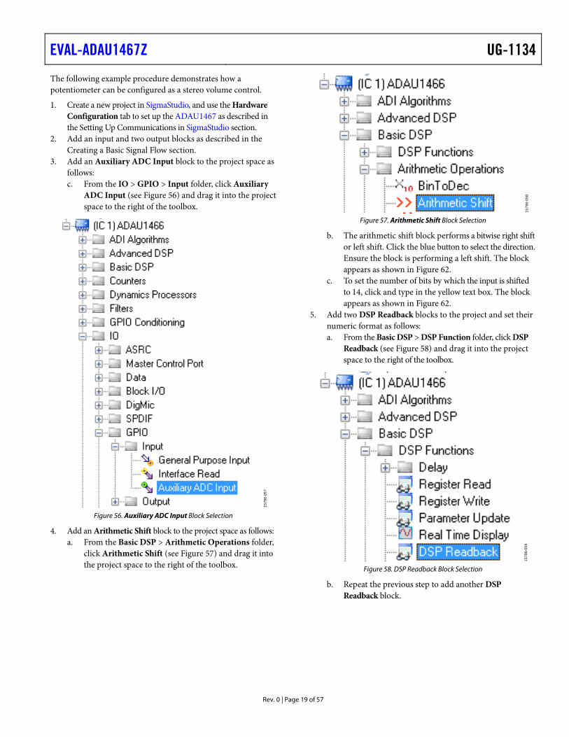
3. Add an Auxiliary ADC Input block to the project space as follows: c. From the IO > GPIO > Input folder, click Auxiliary
ADC Input (see Figure 56) and drag it into the project space to the right of the toolbox.
1578
6-05
7
Figure 56. Auxiliary ADC Input Block Selection
4. Add an Arithmetic Shift block to the project space as follows: a. From the Basic DSP > Arithmetic Operations folder,
click Arithmetic Shift (see Figure 57) and drag it into the project space to the right of the toolbox.
1578
6-05
8
Figure 57. Arithmetic Shift Block Selection
b. The arithmetic shift block performs a bitwise right shift or left shift. Click the blue button to select the direction. Ensure the block is performing a left shift. The block appears as shown in Figure 62.
c. To set the number of bits by which the input is shifted to 14, click and type in the yellow text box. The block appears as shown in Figure 62.
5. Add two DSP Readback blocks to the project and set their numeric format as follows: a. From the Basic DSP > DSP Function folder, click DSP
Readback (see Figure 58) and drag it into the project space to the right of the toolbox.
1578
6-05
9
Figure 58. DSP Readback Block Selection
b. Repeat the previous step to add another DSP Readback block.
c. The DSP Readback block uses the USBi interface to read the value of a signal from the memory of the DSP core as the algorithm is executing. The block passes the signal through from its input to its output unchanged. i. Press the Read button to obtain the instantaneous
value of the signal passing through the block. It is also possible to set the block to poll the value repeatedly. This feature is useful for debugging, but it increases the amount of processing, USB communication, and screen refreshes performed by SigmaStudio substantially. Avoid setting a large number of DSP Readback blocks to read contin-uously because this action may cause the PC to run slowly. Note that this action does not affect the real-time processing on the SigmaDSP core.
ii. On each of the two DSP Readback blocks, click on the blue dot to the left of the Read button to read both blocks continuously (see Figure 59).
1578
6-06
0
Figure 59. Activating Continuous Readback
iii. For one of the DSP readback blocks, change the numeric format used to decode and display of the value of the signal to 32.0 by typing 32 in the left format box then pressing the Tab key. SigmaDSP uses a numeric format of 8.24 for audio signals.
6. Add a Single Slew Ext Volume block to the project space as follows: a. From the Volume Controls > Adjustable Gain >
Clickless HW Slew folder, click Single Slew Ext Vol (see Figure 60), and drag it into the project space to the right of the toolbox.
1578
6-06
1
Figure 60. Single Slew Ext Vol Block Selection
b. By default, the Single Slew Ext Vol block has one audio signal input. To add another channel, right click in the empty white space of the Single Slew Ext Vol block, and
select 1 > 1. Gain (HW slew) > Grow Algorithm from the dropdown menu that appears (see Figure 61).
1578
6-06
2
Figure 61. Growing the Single Slew Ext Vol Block to Two Channels
7. Wire the blocks together as shown in Figure 62. Note that the position of blocks in the diagram does not matter.
8. Click the Link/Compile/Download button (see Figure 29) or press F7 to compile the signal flow and download it to the hardware. The audio signal passes from the S/PDIF receiver through the ASRCs into the DSP and the EQ filter, and then out on the S/PDIF transmitter. To change the settings of the EQ filter, click the blue icon at top of the block. Drag the control slider in SigmaStudio to change the filter gain in real-time while the project is running.
The schematic (see Figure 62) shows audio from input Channel 0 and Channel 1 connected to the input of a volume control block. The volume is controlled by the value of the AUXADC1 channel, which is controlled by the left potentiometer (R1).
The output of the auxiliary ADC on the ADAU1467 is a 10-bit integer value in a 32-bit register. The first DSP Readback block, before the left shift, displays the output of the ADC in 32.0 format, which can be interpreted as 32 integer bits and 0 fractional bits. When the potentiometer is turned fully counter clockwise, this block reads back the minimum ADC output value of 0. When the potentiometer is turned fully clockwise, this block reads back the maximum ADC output value of 1023 (within the range of the component tolerance).
The native audio format of the ADAU1467 is 8.24. In this example, the volume control multiplies the input signal by a fractional value ranging from 0 (silence) to 1 (unity gain). Therefore, the control signal from the ADC must be left shifted 14 bits to scale the maximum value appropriately.
The second DSP Readback block, after the left shift, displays the output of the ADC in 8.24 format, which may be interpreted as 8 integer bits and 24 fractional bits. When the potentiometer is turned fully counter clockwise, this block reads back the minimum ADC output value of 0. When the potentiometer is turned fully clockwise, this block reads back the maximum ADC output value of 1 (within the range of the component tolerance).
EVALUATION BOARD FEATURES The EVAL-ADAU1467Z provides access to the serial ports, S/PDIF interfaces, multipurpose pins, and auxiliary ADCs of the ADAU1467.
AD1937 CODEC One of the four serial input ports and one SDATAIOx pin are connected to the ADCs of the AD1937, and one of the four serial output ports and three SDATAIOx pins are connected to the digital-to-analog converts (DACs) of the AD1937. Each serial data pin carries two channels of serial audio in I2S format, for a total of four channels of analog audio input and eight channels of analog audio output.
AD1937 Boot Mode
The AD1937 is capable of running in standalone mode or being booted and configured through its I2C control port. Switch S2 selects the boot mode of the AD1937 codec as shown in Figure 63, and this switch is set to STANDALONE by default. When running in standalone mode, the serial ports of the AD1937 are configured as clock slaves. Therefore, the corresponding serial ports on the ADAU1467 must be set as clock masters. By default, all serial ports on the ADAU1467 are set as clock masters when a new project is created in SigmaStudio.
Standalone mode eliminates the need for the user to configure the registers of the AD1937 via its I2C port. This mode fixes the sample rate of the AD1937 at 44.1 kHz or 48 kHz. The analog audio inputs and outputs on the EVAL-ADAU1467Z can be distorted or silent if a sample rate other than 44.1 kHz or 48 kHz is used for the ADAU1467 serial ports.
The alternate I2C master port pins of ADAU1467 are connected to the I2C control port of the AD1937 when Switch S2 is set to I2C boot mode; this requires reconfiguration of the master control port from SPI to I2C and enabling the alternate I2C port on the MP24 pin and MP25 pin. This configuration is beyond the scope of this user guide; however, it enables the ADAU1467 to boot and configure all of the control registers of the AD1937. When configured manually, the codec is flexible and can run at any sample rate up to 192 kHz.
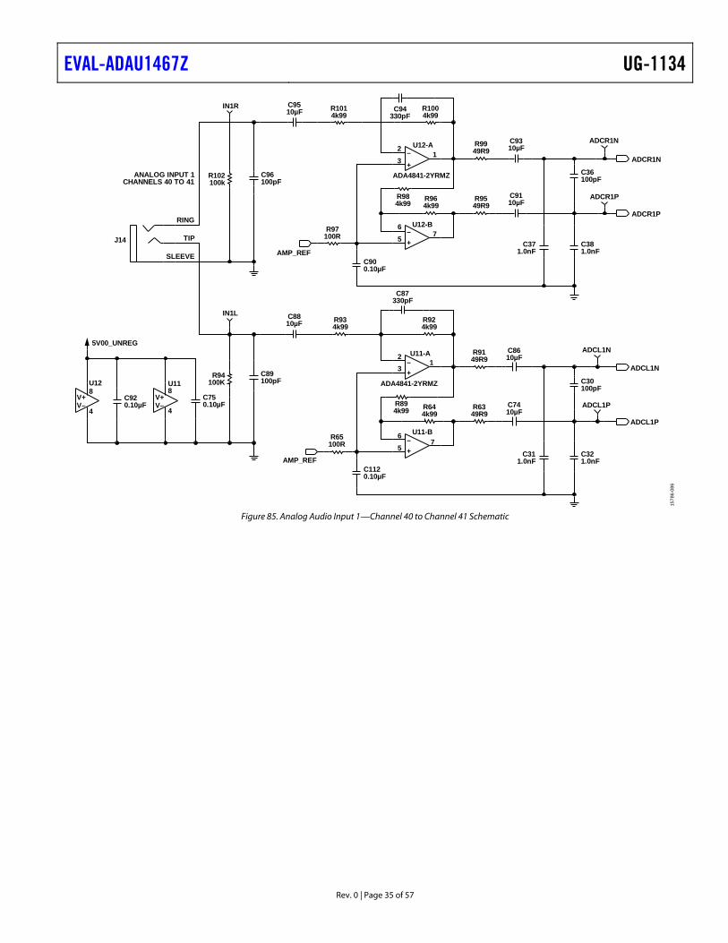
Two stereo input jacks allow four, single-ended, line level, analog input signals. The AD1937 ADC inputs are configured such that the full scale is 2.8 V p-p, which is approximately 1 V rms for a sine wave. Any signal that exceeds 2.8 V p-p at the audio jack is clipped, which creates distortion. The signals are fed to active low-pass filters and converted to differential pairs before reaching the ADCs of the AD1937. The filters are designed for a system sample rate of 44.1 kHz or 48 kHz.
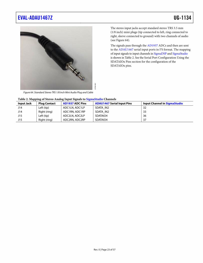
Figure 64. Standard Stereo TRS 1/8 Inch Mini Audio Plug and Cable
The stereo input jacks accept standard stereo TRS 3.5 mm (1/8 inch) mini plugs (tip connected to left, ring connected to right, sleeve connected to ground) with two channels of audio (see Figure 64).
The signals pass through the AD1937 ADCs and then are sent to the ADAU1467 serial input ports in I2S format. The mapping of input signals to input channels in SigmaDSP and SigmaStudio is shown in Table 2. See the Serial Port Configuration Using the SDATAIOx Pins section for the configuration of the SDATAIOx pins.
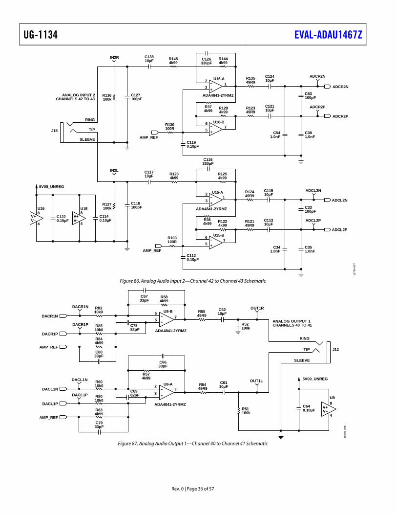
Table 2. Mapping of Stereo Analog Input Signals to SigmaStudio Channels Input Jack Plug Contact AD1937 ADC Pins ADAU1467 Serial Input Pins Input Channel in SigmaStudio J14 Left (tip) ADC1LN, ADC1LP SDATA_IN2 32 J14 Right (ring) ADC1RN, ADC1RP SDATA_IN2 33 J15 Left (tip) ADC2LN, ADC2LP SDATAIO4 36 J15 Right (ring) ADC2RN, ADC2RP SDATAIO4 37
Four stereo output jacks allow eight line level analog output signals. The AD1937 DAC outputs are configured such that a full-scale signal is 2.8 V p-p at the jack, which is approximately 1 V rms for a sine wave. The signals output from the DACs are fed to active low-pass filters and then ac-coupled before reaching the output jacks. The filters are designed for a system sample rate of 44.1 kHz or 48 kHz.
The output filters are designed to drive high impedance loads, for instance, loads at the input to active speakers. Some low impedance loads (for example, loads from headphones) can also be driven by these outputs. However, very low impedance loads (for example, loads from passive speakers) cannot be driven by these outputs.
The stereo output jacks accept standard stereo TRS 3.5 mm (1/8 inch) mini plugs (tip connected to left, ring connected to right, sleeve connected to ground) with two channels of audio (see Figure 64).
The signals pass from the ADAU1467 serial outputs in I2S format to the AD1937 DACs, where they are converted to analog signals and sent through the output filters to the output jacks. The mapping among the SigmaStudio output channels, output serial ports, and output jacks is shown in Table 3.
See the Serial Port Configuration Using the SDATAIOx Pins section for the configuration of the SDATAIOx pins.
Table 3. Mapping of SigmaStudio Channels to Output Jacks Output Jack Plug Contact AD1937 DAC Pin ADAU1467 Serial Output Pin Output Channel in SigmaStudio J12 Left (tip) OL1 SDATA_OUT0 0 J12 Right (ring) OR1 SDATA_OUT0 1 J13 Left (tip) OL2 SDATAIO5 4 J13 Right (ring) OR2 SDATAIO5 5 J18 Left (tip) OL3 SDATAIO6 8 J18 Right (ring) OR3 SDATAIO6 9 J17 Left (tip) OL4 SDATAIO7 12 J17 Right (ring) OR4 SDATAIO7 13
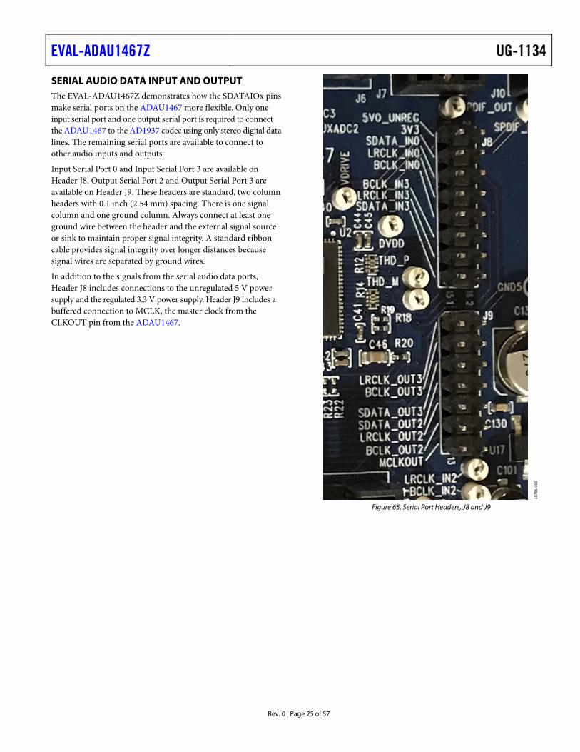
SERIAL AUDIO DATA INPUT AND OUTPUT The EVAL-ADAU1467Z demonstrates how the SDATAIOx pins make serial ports on the ADAU1467 more flexible. Only one input serial port and one output serial port is required to connect the ADAU1467 to the AD1937 codec using only stereo digital data lines. The remaining serial ports are available to connect to other audio inputs and outputs.
Input Serial Port 0 and Input Serial Port 3 are available on Header J8. Output Serial Port 2 and Output Serial Port 3 are available on Header J9. These headers are standard, two column headers with 0.1 inch (2.54 mm) spacing. There is one signal column and one ground column. Always connect at least one ground wire between the header and the external signal source or sink to maintain proper signal integrity. A standard ribbon cable provides signal integrity over longer distances because signal wires are separated by ground wires.
In addition to the signals from the serial audio data ports, Header J8 includes connections to the unregulated 5 V power supply and the regulated 3.3 V power supply. Header J9 includes a buffered connection to MCLK, the master clock from the CLKOUT pin from the ADAU1467.
Figure 66. Multipurpose Pin Function Selection Switches S5 to S8
The multipurpose pins on the ADAU1467 can be used for general-purpose inputs or outputs when configured as such using the ADAU1467 control registers. Of the 14 multipurpose pins, three are connected to switches that pull the pins low or tie them high, three are on test points and connected to high impedance inputs to LED drivers, and two are available headers. The remaining six pins are used for other functionality and are, therefore, unavailable for use as multipurpose pins.
The signal from the LRCLK_OUT1/MP5 pin is fed to an inverter that drives LED D4. The signal from the LRCLK_OUT3/MP9 pin is fed to an inverter that drives LED D3. The signal from the LRCLK_IN1/MP11 pin is fed to an inverter that drives LED D5.
The five multipurpose pins available for use as general-purpose inputs or outputs, along with their access points on the evaluation board, are described in Table 4.
1578
6-06
8
Figure 67. Self Boot Slide Switch
To configure the operation of the multipurpose pins, navigate to the MULTIPURPOSE tab in the Hardware Configuration tab in SigmaStudio (see Figure 68).
1578
6-06
9
Figure 68. Multipurpose Pin Configuration in SigmaStudio
Table 4. Multipurpose Pins and Hardware Access Points Multipurpose Pin Connection Access Point LRCLK_OUT1/MP5 Input to inverter (LED D4) TP56 LRCLK_OUT3/MP9 Input to inverter (LED D3) TP48 LRCLK_IN1/MP11 Input to inverter (LED D5) TP29 LRCLK_IN2/MP12 Pin multiplexed with LRCLK_IN2 Header J3, Pin 4 LRCLK_IN3/MP13 Pin multiplexed with LRCLK_IN3 Header J2, Pin 4
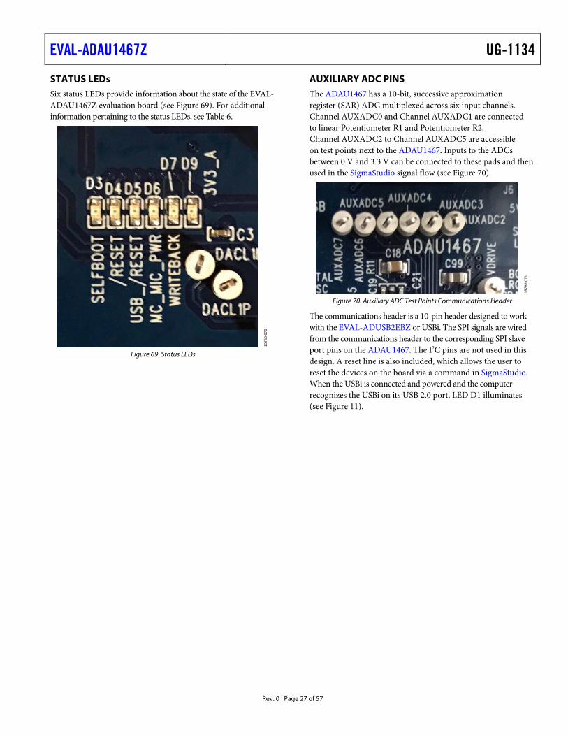
STATUS LEDs Six status LEDs provide information about the state of the EVAL-ADAU1467Z evaluation board (see Figure 69). For additional information pertaining to the status LEDs, see Table 6.
1578
6-07
0
Figure 69. Status LEDs
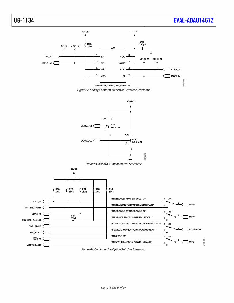
AUXILIARY ADC PINS The ADAU1467 has a 10-bit, successive approximation register (SAR) ADC multiplexed across six input channels. Channel AUXADC0 and Channel AUXADC1 are connected to linear Potentiometer R1 and Potentiometer R2. Channel AUXADC2 to Channel AUXADC5 are accessible on test points next to the ADAU1467. Inputs to the ADCs between 0 V and 3.3 V can be connected to these pads and then used in the SigmaStudio signal flow (see Figure 70).
1578
6-07
1
Figure 70. Auxiliary ADC Test Points Communications Header
The communications header is a 10-pin header designed to work with the EVAL-ADUSB2EBZ or USBi. The SPI signals are wired from the communications header to the corresponding SPI slave port pins on the ADAU1467. The I2C pins are not used in this design. A reset line is also included, which allows the user to reset the devices on the board via a command in SigmaStudio. When the USBi is connected and powered and the computer recognizes the USBi on its USB 2.0 port, LED D1 illuminates (see Figure 11).
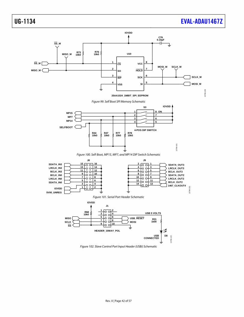
SELF BOOT A 1 Mb, 20 MHz, SPI, serial EEPROM memory is included on the EVAL-ADAU1467Z evaluation board. The ADAU1467 is capable of booting and executing a program without help from an external microcontroller. This feature allows any project developed within SigmaStudio to execute when the ADAU1467 powers up or on a rising edge of the RESET pin. Position 1 of Switch S3 switch, the top position of the DIP switch (see Figure 71), sets the state of the SELFBOOT pin of the ADAU1467, which determines whether a self boot operation occurs.
1578
6-07
2
Figure 71. Self Boot Slide Switch
To use the self boot functionality, take the following steps:
1. Add an E2Prom block to the project space of the Hardware Configuration tab. From the Processors (ICs/DSPs) folder, click E2Prom (see Figure 72) and drag it into the project space to the right of the toolbox.
1578
6-07
3
Figure 72. E2Prom IC Selection in SigmaStudio
2. Connect the green input pin of the E2Prom IC to one of the available blue output pins of the USB Interface block.
3. Set the communication mode to SPI 0x1 ADR0 (see Figure 73). (There is no physical connection between the USBi connector and the EEPROM on the EVAL-ADAU1467Z. SigmaStudio writes a small program to the ADAU1467, which then writes the self boot data from the master SPI port to the EEPROM.)
1578
6-07
4
Figure 73. E2Prom Setup in the Hardware Configuration Tab
4. Before downloading the self boot data to the EEPROM, click the Link-Compile-Download button (see Figure 29) or press F7 to compile the SigmaStudio project file.
5. When writing to the EEPROM, set the self boot switch (Position 1 of Switch S3) to the disabled position.
6. Right click the empty white space in the ADAU1467 IC block in the Hardware Configuration tab of SigmaStudio. From the menu that appears, select Self-boot Memory, then Write Latest Compilation through DSP (see Figure 74).
Figure 74. Writing to the EEPROM Through the ADAU1467 Master SPI Port
1578
6-07
8
Figure 75. External Memory Erase and Overwrite Warning Window
7. An EEPROM Properties dialog box appears. Enter the appropriate values into the text fields as shown in Figure 76, then click OK.
1578
6-07
6
Figure 76. EEPROM Properties Window and Required Settings
8. A warning dialog box appears to remind the user that executing an external memory write erases and overwrites any data currently stored on the EEPROM (see Figure 75). Click OK to proceed.
9. SigmaStudio begins the EEPROM write operation. This operation can take several minutes to complete (see Figure 77). When the status window disappears, the operation is complete.
1578
6-07
7
Figure 77. External Memory Write Operation Status Window
To execute a self boot operation, take the following steps:
1. Set the self boot switch (S2) to enabled. 2. Press and release the RESET push-button (S1).
A self boot operation is then performed, and the ADAU1467 runs a program.
RESET To manually reset the ADAU1467 and AD1937, press and release the RESET push-button, S1 (see Figure 78). A reset generator circuit toggles the reset pins on the ADAU1467 and AD1937 to perform a full hardware reset of both devices.
1578
6-07
9
Figure 78. Manual Reset Push-Button
To generate a reset in software, right click in the empty white border of the USB Interface block in the Hardware Configuration tab, and then choose Device Enable/Disable from the menu that appears (see Figure 79). Performing this action sets the system reset signal to logic low.
1578
6-08
0
Figure 79. Toggling the Reset Signal in SigmaStudio
SERIAL PORT CONFIGURATION USING THE SDATAIOx PINS The SDATAIOx pins provide additional serial audio data inputs or outputs and expand the functionality and versatility of the serial ports. In earlier generations of the SigmaDSP architecture, serial ports are limited to a single SDATA pin. If this serial data pin is configured in a stereo mode, the remaining channels associated with the port are inaccessible. Device interfaces with a single LRCLK and BCLK pair and multiple stereo data lines (for example, in a case with multiple connections in the I2S format) required using multiple SigmaDSP serial ports.
The SDATAIOx pins on the ADAU1463 and ADAU1467 eliminate this bottleneck. The connection between the SigmaDSP and the AD1937 codec uses four I2S data lines for the eight DAC channels and two I2S data lines for the four ADC channels. The EVAL-ADAU1467Z supplements the SDATA_OUT0 pin with three SDATAIOx pins and the SDATA_IN2 pin with one SDATAIOx pin. This configuration connects all of the audio channels of the AD1937 while using only one input serial port and one output serial port. The connections are shown in Figure 80.
8-CHANNELDAC
(4 × I2S)
4-CHANNELADC
(2 × I2S)
AD1937CODEC
ANALOG OUT
ANALOG IN
DAC FRAME SYNC
DAC BIT CLOCK
OUTPUT CHANNELS 0-1
OUTPUT CHANNELS 4-5
ADC FRAME SYNC
ADC BIT CLOCK
INPUT CHANNELS 32-33
INPUT CHANNELS 36-37
OUTPUT CHANNELS 8-9
OUTPUT CHANNELS 12-13
1578
6-08
1
LRCLK_OUT0
BCLK_OUT0
SDATA_OUT0
LRCLK_IN2
BCLK_IN2
SDATA_IN2
SDATAIO4
SDATAIO6
SDATAIO7
ADAU1467
SDATAIO5
Figure 80. Serial Ports Connections to the AD1937 Codec
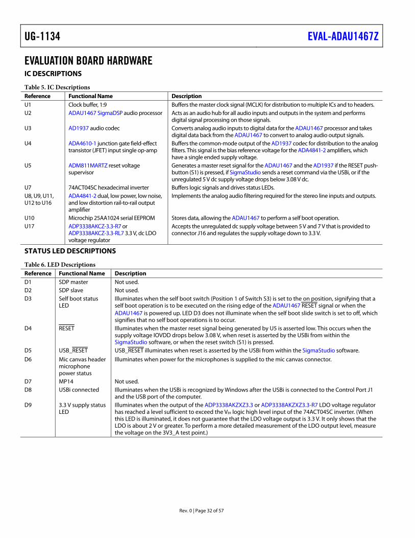
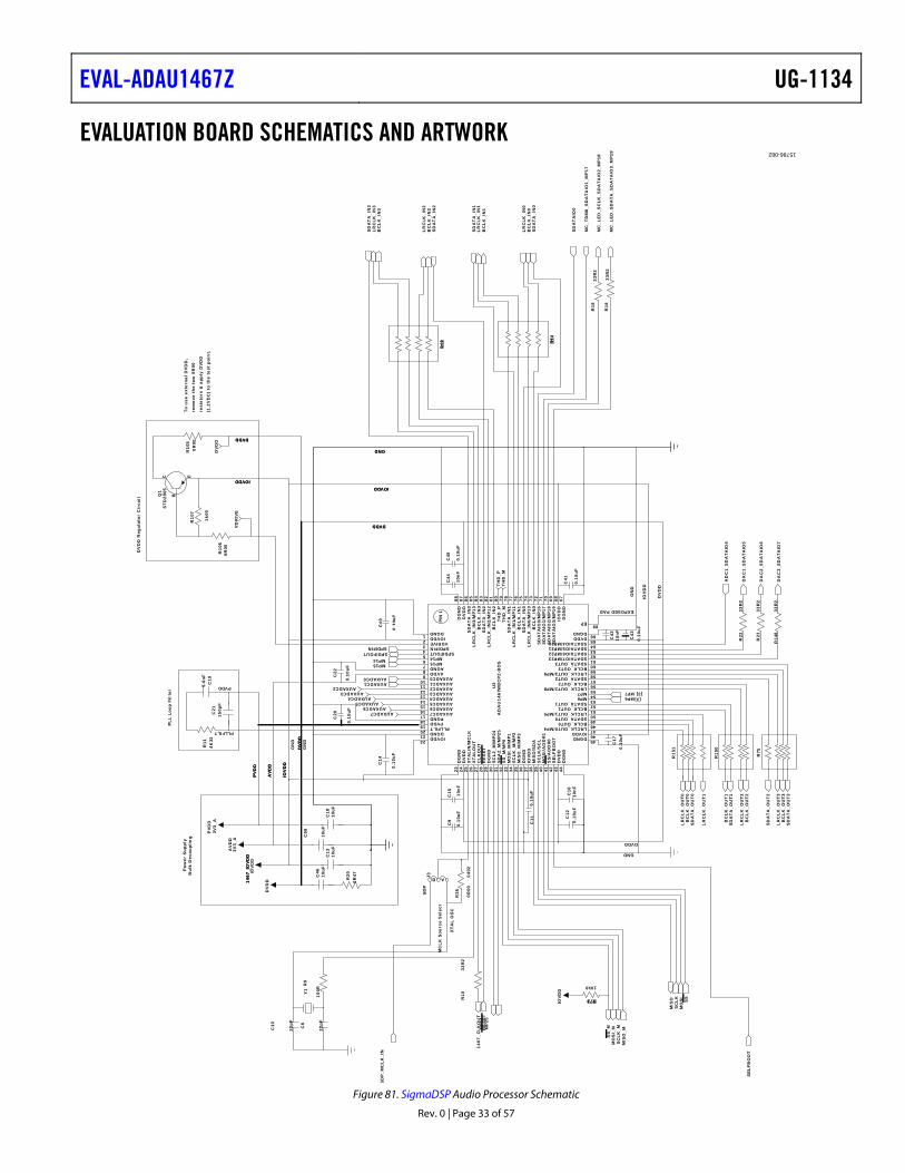
Table 5. IC Descriptions Reference Functional Name Description U1 Clock buffer, 1:9 Buffers the master clock signal (MCLK) for distribution to multiple ICs and to headers. U2 ADAU1467 SigmaDSP audio processor Acts as an audio hub for all audio inputs and outputs in the system and performs
digital signal processing on those signals. U3 AD1937 audio codec Converts analog audio inputs to digital data for the ADAU1467 processor and takes
digital data back from the ADAU1467 to convert to analog audio output signals. U4 ADA4610-1 junction gate field-effect
transistor (JFET) input single op-amp Buffers the common-mode output of the AD1937 codec for distribution to the analog filters. This signal is the bias reference voltage for the ADA4841-2 amplifiers, which have a single ended supply voltage.
U5 ADM811MARTZ reset voltage supervisor
Generates a master reset signal for the ADAU1467 and the AD1937 if the RESET push-button (S1) is pressed, if SigmaStudio sends a reset command via the USBi, or if the unregulated 5 V dc supply voltage drops below 3.08 V dc.
U7 74ACT04SC hexadecimal inverter Buffers logic signals and drives status LEDs. U8, U9, U11, U12 to U16
Implements the analog audio filtering required for the stereo line inputs and outputs.
U10 Microchip 25AA1024 serial EEPROM Stores data, allowing the ADAU1467 to perform a self boot operation. U17 ADP3338AKCZ-3.3-R7 or
ADP3338AKCZ-3.3-RL7 3.3 V, dc LDO voltage regulator
Accepts the unregulated dc supply voltage between 5 V and 7 V that is provided to connector J16 and regulates the supply voltage down to 3.3 V.
STATUS LED DESCRIPTIONS
Table 6. LED Descriptions Reference Functional Name Description D1 SDP master Not used. D2 SDP slave Not used. D3 Self boot status
LED Illuminates when the self boot switch (Position 1 of Switch S3) is set to the on position, signifying that a self boot operation is to be executed on the rising edge of the ADAU1467 RESET signal or when the ADAU1467 is powered up. LED D3 does not illuminate when the self boot slide switch is set to off, which signifies that no self boot operations is to occur.
D4 RESET Illuminates when the master reset signal being generated by U5 is asserted low. This occurs when the supply voltage IOVDD drops below 3.08 V, when reset is asserted by the USBi from within the SigmaStudio software, or when the reset switch (S1) is pressed.
D5 USB_RESET USB_RESET illuminates when reset is asserted by the USBi from within the SigmaStudio software.
D6 Mic canvas header microphone power status
Illuminates when power for the microphones is supplied to the mic canvas connector.
D7 MP14 Not used. D8 USBi connected Illuminates when the USBi is recognized by Windows after the USBi is connected to the Control Port J1
and the USB port of the computer. D9 3.3 V supply status
LED Illuminates when the output of the ADP3338AKZXZ3.3 or ADP3338AKZXZ3.3-R7 LDO voltage regulator has reached a level sufficient to exceed the VIH logic high level input of the 74ACT04SC inverter. (When this LED is illuminated, it does not guarantee that the LDO voltage output is 3.3 V. It only shows that the LDO is about 2 V or greater. To perform a more detailed measurement of the LDO output level, measure the voltage on the 3V3_A test point.)
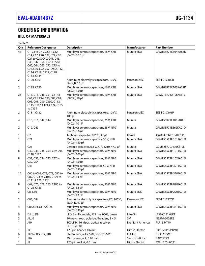
1 J11 120-pin header, 0.6 mm Hirose Electric FX8-120P-SV1(91) 6 J12 to J15, J17, J18 Stereo mini jacks, SMT, SJ-3523-SMT CUI Inc. SJ-3523-SMT 1 J16 Mini power jack, 0.08 inch Switchcraft Inc. RAPC722X 1 J2 120-pin socket, 0.6 mm Hirose Electric FX8-120S-SV(21)
ESD Caution ESD (electrostatic discharge) sensitive device. Charged devices and circuit boards can discharge without detection. Although this product features patented or proprietary protection circuitry, damage may occur on devices subjected to high energy ESD. Therefore, proper ESD precautions should be taken to avoid performance degradation or loss of functionality.
Legal Terms and Conditions By using the evaluation board discussed herein (together with any tools, components documentation or support materials, the “Evaluation Board”), you are agreeing to be bound by the terms and conditions set forth below (“Agreement”) unless you have purchased the Evaluation Board, in which case the Analog Devices Standard Terms and Conditions of Sale shall govern. Do not use the Evaluation Board until you have read and agreed to the Agreement. Your use of the Evaluation Board shall signify your acceptance of the Agreement. This Agreement is made by and between you (“Customer”) and Analog Devices, Inc. (“ADI”), with its principal place of business at One Technology Way, Norwood, MA 02062, USA. Subject to the terms and conditions of the Agreement, ADI hereby grants to Customer a free, limited, personal, temporary, non-exclusive, non-sublicensable, non-transferable license to use the Evaluation Board FOR EVALUATION PURPOSES ONLY. Customer understands and agrees that the Evaluation Board is provided for the sole and exclusive purpose referenced above, and agrees not to use the Evaluation Board for any other purpose. Furthermore, the license granted is expressly made subject to the following additional limitations: Customer shall not (i) rent, lease, display, sell, transfer, assign, sublicense, or distribute the Evaluation Board; and (ii) permit any Third Party to access the Evaluation Board. As used herein, the term “Third Party” includes any entity other than ADI, Customer, their employees, affiliates and in-house consultants. The Evaluation Board is NOT sold to Customer; all rights not expressly granted herein, including ownership of the Evaluation Board, are reserved by ADI. CONFIDENTIALITY. This Agreement and the Evaluation Board shall all be considered the confidential and proprietary information of ADI. Customer may not disclose or transfer any portion of the Evaluation Board to any other party for any reason. Upon discontinuation of use of the Evaluation Board or termination of this Agreement, Customer agrees to promptly return the Evaluation Board to ADI. ADDITIONAL RESTRICTIONS. Customer may not disassemble, decompile or reverse engineer chips on the Evaluation Board. Customer shall inform ADI of any occurred damages or any modifications or alterations it makes to the Evaluation Board, including but not limited to soldering or any other activity that affects the material content of the Evaluation Board. Modifications to the Evaluation Board must comply with applicable law, including but not limited to the RoHS Directive. TERMINATION. ADI may terminate this Agreement at any time upon giving written notice to Customer. Customer agrees to return to ADI the Evaluation Board at that time. LIMITATION OF LIABILITY. THE EVALUATION BOARD PROVIDED HEREUNDER IS PROVIDED “AS IS” AND ADI MAKES NO WARRANTIES OR REPRESENTATIONS OF ANY KIND WITH RESPECT TO IT. ADI SPECIFICALLY DISCLAIMS ANY REPRESENTATIONS, ENDORSEMENTS, GUARANTEES, OR WARRANTIES, EXPRESS OR IMPLIED, RELATED TO THE EVALUATION BOARD INCLUDING, BUT NOT LIMITED TO, THE IMPLIED WARRANTY OF MERCHANTABILITY, TITLE, FITNESS FOR A PARTICULAR PURPOSE OR NONINFRINGEMENT OF INTELLECTUAL PROPERTY RIGHTS. IN NO EVENT WILL ADI AND ITS LICENSORS BE LIABLE FOR ANY INCIDENTAL, SPECIAL, INDIRECT, OR CONSEQUENTIAL DAMAGES RESULTING FROM CUSTOMER’S POSSESSION OR USE OF THE EVALUATION BOARD, INCLUDING BUT NOT LIMITED TO LOST PROFITS, DELAY COSTS, LABOR COSTS OR LOSS OF GOODWILL. ADI’S TOTAL LIABILITY FROM ANY AND ALL CAUSES SHALL BE LIMITED TO THE AMOUNT OF ONE HUNDRED US DOLLARS ($100.00). EXPORT. Customer agrees that it will not directly or indirectly export the Evaluation Board to another country, and that it will comply with all applicable United States federal laws and regulations relating to exports. GOVERNING LAW. This Agreement shall be governed by and construed in accordance with the substantive laws of the Commonwealth of Massachusetts (excluding conflict of law rules). Any legal action regarding this Agreement will be heard in the state or federal courts having jurisdiction in Suffolk County, Massachusetts, and Customer hereby submits to the personal jurisdiction and venue of such courts. The United Nations Convention on Contracts for the International Sale of Goods shall not apply to this Agreement and is expressly disclaimed.