hllfJltgtOlI ~ rwfMd flttuull of~ ~fId bvtfl ~ of It4IIJlt 51 Q~_I ~hoII tIto U 51 11 Ou 1 ltOf -laquoIf IiOf 0 tt-t ItO(Iloy_ oWt
_ bull h V~ II tIIId fll n fty _1 laquoHIot III ~~I ilt thoo -
(tIVi_ If llJh_ 0 jIIIy Iiolt1f ~l rw-d (Wrlo_ ttr~ _111 t h lt1lt1 )1 gtf1~ I middot~ ~ I~H R- fI( to I-Ior
ltom IOO-I tf~ nlt ~P by l~J 1~ t lfIll1~ (ll 0--
roof ntot lv 01101 or 01 1 ~If rtl~-OI W 19 by ~lfd $f u VIW1 llI rly ~y ( T- Yoewi ftd Ofunront Of fIOi pound1 IIIttI Ikl flOf
ly f~ ~w ffl(l ThC f hIt vnflaquo1 St~ ~I ~yen r- IIO
EXAMINATION RESULTS ON IMJ-2 LPIVI CHARGE CONVERTERS YM-AMP-7023 AND YM=AMP-7025
__ ~-~ ~middotwon -
NOTICI
Michael B Murphy Richard E Helntzleman
Sandia National Laboratories Albuquerque New Mexico 87185
November 1982
PORnON OFTHIS REPORT ARE ILLEGIBLE It fill been reproduced from the bcsfavailabl copy to Ponlt the broadeat possibl IVIII-11raquo1f1tJ
Published on Behalf of the GEND Group by
EGampG Idaho Inc Idaho Falls Idaho 83416
Prepared for the US Department of Energy
Three Mile leland Operations Office Under DOE Contract No DEmiddotAC07middot78ID01amp70
nSffiI~li10~ Of 1lIS OncutA(~l ISmiddot
ABSTRACT
During and for several months after the Three Mile Island Unit 2 accident the reactor vessel and two steam g~nerators were closely monitored for the existence of coolant system loose parts We have examined two Endevco charge converters removed from the loose parts monitoring system inside containment and found the devices to be severely degraded by gall11la radiation Because of this it is likely that the loose parts readings made during the accident were lower than actual levels This report discusses the cause of failure our estimates of the total gamma radiation doses received by the charge converters and our recommendations for changes 1n US Nuclear Regulatory Guide 1133
3
middot_-__----bull -
CONTENTS
I INTRODUCTION AND SUMMARY FINDINGS A Findings and Recommendations
II DESCRIPTIOM A Rockwell lPM System at TMI-2
B Operational History
C Charge Converter Mechanical Descrfption
D Charge Converter Functional Description
III ELECTRICAL EVALUATION A Test Sequence
B Evaluation of YM-AMP-7025
C Evaluation of YM-AMP-7023
D Effect of Degradationon Circuit Operation
IV FAILURE MODE AND RADIATION DOSE A Failure Mechanism
B Total Dose
v COfIiIENT
7
9
10
10
11
14
14
17
18
21
21
25
APPENDIX A Unit 2 305 Elevation Floor Plan 26
APPENDIX B Outli neDrawing of Eridevco Remote Charge Converter 27
APPENDIX C Manufacturers Specification Listing for the HEM 511 28
3 Charge ConverterSchemaHc 4 Model 4479~ 1 Line Driver Condit1oner Schematic 5 Endevco Model 2652 Test Set-up 6 YM-AMP-7025 Osc1lloscope Trac1ngs 7 YM-AMP-7025 Transfer Characterist1c 8 YM-AMP-7023 Transfer Characterist1c 9 linear Operat1ng Region vs Gamma Dose 10 VGSth Shift with Gamma Dose 11 MEM 511 Annealing Character1stics
Tables
1 DC Operating Point Measurements 2 Room Temperature Anrieali ng
9
11
13
13
14
15
15
17
19
23
23
16
22
I INTRODUCTION AND SUMMARY FINDINGS
This report contains the results of our laboratory examinations of two Endevco Model 2652M4 Remote Charge Converters which were removed from the Three Mile Island Unit 2 (TMI-2) conta1nment building in November 1980 In situ testing done in ~ptember 1980 indicated that both charge converters h~ving TMI-2 tag numbers YM-AMP-7023 and YM-AMP-7025 were inoperable at the t1me of the measureshyments 1 Records obtained in the accident time frame indicate that all eight Rockwell steam generator loose parts monitoring (LPM) channels each containing Endevco charge converters may have failed or were close to failure during the first few days of the TMI-2 accident 23 This is ind1cated by the need on April 2 1979 to increase channel gains and a few weeks later the measurement of inappropriately high bias voltages
The charge converters were mounted inside protective boxes on t~e outside of the 0 ring wall on the 305 foot elevation near the personnel hatch of the TMI-2 containment build1ng (see Appendix A) They were removed for laboratory examination because they had failed they contain radiat10n sensitive HDS trans1stors known to be useful as radiation dosimeters and they were l~a5ily
accessible bull This report is not meant to evaluate the entire LPM system Here we discuss the cause of failure of the charge converters and the implications of this on loose parts monitoring We also make est1mates of the total gamma radiation doses recei ved by each charge converte r ~
-A Findings and Recommendations
1 Both charge converters wJr~ d~graded by ~adiation probably in the first few days of the accident to th~middot extent that YM-AMP-7025 was non-funttional ~~d YM-AMP-7023 was marginally funtt1orlaT The degradation 1n both ases wasmiddot caused by a large upward sh1ft in the gate-to-source threshold voltage of the MEM 511 transistor used 1n the Q2 slot This can result 1n an indication of lower vibration levels than are actually there The MEM 511 is an MOS f1eld effect tranSistor and like all non-hardened I()S transistors it is quite sens1t1ve to rad1at10n dose Our tests 1nd1cate that because uf this tranSistor these charge converters are usable up to only approdmately bIOS rads
2 The fa1lure mode observed in these charge converters 1s espeCially 1ns1d10us since the LPM channel can appear to operate properly even a ftef severe
7
8
degradation has occurred The only normal indication of this condition is that the usual background vibration levels would appear to decrease Fortunately the condition can be detected remotely by measuring the charge converter DC bias voltage and looking for a higher than normal level The normal bias voltage 1s about 135 volts This voltage will shift upwards as radiation dose is accumulated until in the limit the power supply rail (normally 30 volts) is reached We recommend that all power plant operators using this and similar model Endevco charge converters perform the above measurements to determine the state-of-health of their LPM systems This same problem has been observed in operat1ng plants where the charge converters are located in high rad1at10n fields 3
3 We recommend that Endevco Model 2652M4 charge converters other s1mllar Endevco models and other manufacturers models which cannot survive low radiation exposure be removed from nuclear power plants and replaced with more radiation tolerant designs MOS transistors should not be used in any appl lCyti~n where inherent or potential radiation exposure is possible
4 We recommend that U S Nuclear Regulatory Guide 1133 be modified to strongly encourage the use of radiation resistant LPM systems The May 1981 Revision 1 guide states Early detectiol) (of loose parts) can provide the time requi red to avoid or mitigate safetgt-related damage to ormaHunctions of primary system components4 This statement is actually relevant fora power plant operating normally as well as during an acciderit During an accident where operators do not have access to the containment building the LPM system can potentially provide a much needed indication of vibration andor impact levels Operators can use this information to possibly m1tigate further damage The Guide should specify design goal radiation levels which are consistent with those required for Class IE equipment
5 The degradation in VGS(th) of the MOS transistors indicates that YM-AMP-7023 and YM-AMP-7025 received toUl gamma doses of 18xl0S and 54xlOS Rads respectively These levels correlate well with the estimate of 2SxlOS rads received by radiation detector HP-R-211 located near-by
-----------------------_
II DESCRIPTION
A Rockwell lPM System at TMI-2
The Rockwell lPM System at TMI-2 uses a total of eight channels to monitor
the upper and lower tube sheets of the two steam generators Signals from these channels are processed 1n a Rockwell electronics cabinet located in the cable
spreading room Alarms and a channel selectable audio output are located in the control room Each channel consists of an Endevco Model 2276 accelerometer mountshy
ed on the tube sheet and an Endevco Model 2652M4 charge converter mounted outside the O-ring A photograph of the charge converter is shown in Figure 1 The accel- erometers are exposed to high temperatures and radi at ion while the charge con verters are in much 1 ess severe envi ronments The norma 1 rad i at i on fie 1 d a round
the charge converters is on the order of 1 to 10 mRadhr YM-AMP-7023 and YM-AMP-7025 a re used to mon i tor oppos i te sides of steam generator B upper tube sheets The$e are connected to the Rockwell cabinet by approximately 110 meters and 200 meters of coaxial cable respectively
1 YM-AMP-1025 ~te Charge Con~erter Actual size is 57 cm x 222 em Signal input connector shown
9
I
10
B Operational History
We have not attempted to piece together a precise operational history of the LPM channels however we will provide a sketch of information given to us 235 The LPM system as described above was calibrated and operational at the time of the accident The day after the accident a team of Babcock and Wilcox (BampW) technicians were dispatched to TMI-2 to monitor and record the LPM outputs They replaced the Rockwell readout system with a BampW system having a magnetic tape recorder and various filters and signal conditioning electronics The channels were monitored quite closely during the first week following the accident and then at least daily for the remainder of April 1979 The channels were then monitored periodically for several months During the month-long vigil most of the channels were believed at the time to be functional ie normal sounds were heard At the time in situ testing on YM-AMP-7023 and YM-AMP-7025 was done we were informed by GPU that 7 of 8 channels were inoperable Indeed the in situ data show both YM-AMP-7023 and YM-AMP-7025 to be severely degraded or inoperable (see Section III )
On reviewing the information we have it appears that most of the channels had severe degradation within a day or days after theacciClent began This is indicated by the need to adjust the bias levels to 100 It appears that this was necessary the day after the accident began although we know of no written records of this Several weeks after the accident these bias levels were recorded and all were near 100 Another indicator of degradation was the need by BampW to increase channel gains on April 1 and 2 1979
C Charge Converter Mechanical Description
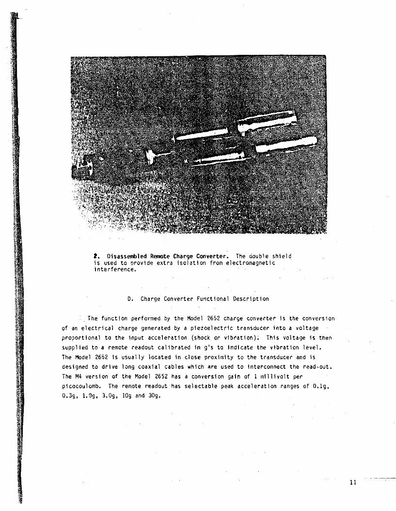
The Endevco Model 2652M4 charge converter is shown disassembled in Figure Z This particular unit is YM-AMP-7025 The electronic circuitry is potted and housed inside a metal tubular case 4~ cm long and 19 cm in diameter The case is actually an outer housing over an inner shield housing with the two being electrically isolated from each other The Microdot(R) connector and BNC connector are electrically grounded to the inner shield case An outline drawing is given in Appendix B
2 Disassembled Remote Charge Converter The double shield is used to provide extra isolation from electromagnetic interference
D Charge Converter Functional Description
The funct i on perfotmed by the Mode I 2652 cha rge converter is the con velS i on of an electrical charge generated by a piezoelectric transducer into a voltage proportional to the input acceleration (shock or vibration)~ This voltage is then supplied to a remote readout calibrated in gs to Indicate the vibration level The Model 2652 is usually located in close proximity to the transducer and is designed to drive long coaxial cables which are used to interconnect the read-out The M4 version of the Model 2652 has a conversion gain of 1 millivolt per picocoulomb The remote readout has selectable peak acceleration ranges of Olg 03g LOg 30g 109 and 30g
11
12
Figure 3 shows a schematic of the charge converter The output line serves both to supply DC power to the device and to carry the AC output signal to the remote readout The circu1t conststs of a very high tnput impedance input amplifier (Ql) a second amplifier (Q2) and a low output impedance line driver (03) In operation the output AC voltage which occurs as a result of the charge Input signal is fed back to the input via CI The polar1ty 15 such as to ma1ntain the voltage at the 1nput near zero Th1s means that the Input charge is stored on
capacitor CI and thus the output voltage eo(t) is given by
eo(t) bull - - q(t) CI
Where q(t) is the Input charge The advantage of this feedback arrangement is to effectively swamp out input cable capacitance vcriations w1th a large capacitor The circuit gain of this particular circuit 15
Eo bull I bull 1 bull Imv Q TI lOOOpf pc
The 2652M4 is biased with the constant current source 01 shown 1n F1gure 4 Th1s circu1t nominally drives the 2652M4 with 8 milliamperes DC The DC compliance voltage 15 set by selection of R6 1n Figure 3 and is nominally 135 volts Resistor
R6 is used to adjust the drain current of 01 so that the voltage drop across RS is sufficient to overcome the gate-to-source threshold voltage (VGSth) of transistor 02 The threshold volt~ge of th MEM 511 is nominally -45 volts Since the circuit is being dr1ven by a curt-ent source the DC voltage (compliance Voltage) appearing across the circuit from output to ground (Pin 2 to Pin 3) will rise until the circuit does in fact draw 8 mil11amperes Th1s happens because an increase In the b1as ~oltage t~nds to turn 02 on harder and more base current Is suppl1ed to Q3 causing 1t to sink the requi red 8 milliamperes This method of neglit ive DC feedback is normally very good in stabiliz1ng the operating points of the three transistors against 1uiat10ns in temperature and component parameters As we will see later the increase in VGSth of Q2 caused by radiation results in the need for the compliance voltage to rise 1n order to keep Q2 on
bull bull bull
I I
I I -Ll II
INPuT I I RI I t IKM
tlOl a4 I I kC RI I I 3 INlt4S 3 1 I 1 _____________ L __________ I I I 1 _________________________ ---I
$IGNAl GAD
__ ___ ~~ _______ --- _____ -J __
3 Charge Converter Schemat1c The ope rat 1 ng poi nt measureshyments in Table were made at thr points indicated by letters ABC D Q2 an MEM 511 MOS transistor was found to be degraded by radiation
QI
4 Model 44191 Une Drher Conditioner Sch_tic Trans1stor Q1 is configured as a constant current generator providing the bias current to the Remote C~arge Converter through pin 12 of the connector
13
14
III ELECTRICAl EVAlUATION
In th1s sect10n we descr1be the electr1cal evaluations performed on YM-AMP-7025 and YM-AMP-7023 and d1scuss the cause of degradation or fa1lure We found that YM-AMP-7025 was completely non-operational and YM-AMP-7023 had output d1stortion for acceleration levels in excess of 19 The cause of fa1lure was found to be radiat10n degradat10n of the MEM 511 MOS transistor used in the 02 slot
A Test Sequence
Both YM-AMP-7025 and YM-AMP-7023 charge converters (Endevco SN ZB47 and ZB50) were found to be slightly contaminated upon arrival from Three Mile Island Each was carefully scrubbed using alcohol before any electrical tests were done and care was taken to avoid getting alcohol inside the Microdot or BNC connectors After decontamination the two devices were taken to the laboratory for the electrical examination Each underwent passive and powered testing before d1section and troubleshooting The passive and powered in situ tests performed at TMI-2 indicated normal resistance and capacitance values but abnormal bias currents and voltages There was no AC output from YM-AMP-7025 Our examination verified the in situ measurements and provided additional data because we could use a calibrated input stimulus
B Evaluation of YM-AMP-7025
Electrical evaluation of the Model 2652 requires a charge generator to provide a~ input signal and a DC source to provide power The test set-up shown in Figure 5 was used for testing as it is recommended by the manufacturer for 2652 operational checkout A schematic of the Endevco 44791 signal conditioner used is shown in Figure 4
0 bullbull 11 1000111
ff4rmiddotl--~I+-I~ bullbullbull j
---_
5 Model 2652 Set-up This set-up is identical to that recommended by Endevco except that the Charge Conshyverter output is monitored instead of the 44791 output 6
(a) (b)
6 YM-AMP-7025 Osci11oscopeTracings These actual photographs of the Charge Converter input and output signals illustrate the non-linear operating mode of YM-AMP-7025 The waveforms shown in (a) are for an input level (lower trace) equivalent to 13 gs peak For this input signal the output (upper trace) would indishycate about 01g peak Tracing (b) shows an equivalent input level of 20gs peak and the distorted output indicating perhaps 25g peak
Initial AC measurements were made using a 1 kilohertz variable amplitude source We found that the charge converter output was essentially zero until quite large input signals were applied Even then the output was severely attenuated and distorted The output positive going portion of the sine wave was found to be more attenuated than the negative going portion This is shown in the oscilloscope pictures in Figure 6 Figure 7 shows a plot of the AC voltage transfer characteristic where the amplitudes of the positive peaks and negative peaks are plotted for various input peak voltages The amplitude of the negative gOing port i on of the output signal is on 1y correct at hi gh signa ~ 1 eve 1 s The amp 1 itude of the positive going portion is always attenuated At this point the unit was disected so that the DC operating points could be determined 10o~---L~~~~~--~~~~~~--~--~~~~
shy
IOlA~t
shy
-
NEGAH VE PfAKS __ PO I TVE PEAK
7 YM-AMP-7025 Transfer Character-1stics The charge amp 11fi er output peak magnitude is plotted versus input peak amplitude The ideal and post reshypair characteristic is shown dotted With the degraded trans stor both positive going peaks and negative going peaks are attenushyated Equivalent input g levels are also shown
15
Hi
The Model 2652 is housed in a double shielded metal enclosure and requires the use of a cutting disc to remove the case shield The unit was potted in an amber epoxy compound which was easily spot-removed by applying heat and crumbling with a soldering iron Points of interest were exposed in this manner These points are shown on the circuit schematic as ABC and O DC voltages were measured at these points and at the output 7 Also the DC input current into pin 2 was measured The recorded values are shown in Table 1 under the heading YM-AMP-7025 pre-repair
VOLTAGE at A 4399 VOLTS 1722 VOLTS 4297 VOLTS 1 712 VOLTS
VOLTAGE at B 2025 VOLTS 6871 VOLTS 1910 VOLTS 6808 VOLTS
VOLTAGE at C 0156 VOLTS 1585 VOLTS 1385 YOLfS 1634 VOL T5
VOLTAGE at 0 5085 VOLTS 2514 VOLTS 4711 VOLTS 2273 VOLTS
VOLTAGE at 2 -ltOutput Bias) 2926 VOLTS 1142 VOLTS 2872 VOLTS 1143 VOLTS
CURRENT into 2 (I nput Current) 0484 mAmps 788 mAmps 2amp0 mAmps 784 mAmps
TAlltE 1 DC OPEIlATlIIG POlIO IIASUREIIIITS
Analysis of the DC measurements indicated that a shift in the DC operating pOint had occurred The output bias (voltage at pin 2) had shifted upward to 2928 volts from a nominal value of 135 volts and the input current had decreased to 0484 milliamperes from a nominal 80 milliamperes The voltage at point C was insuff1cient to b1as Q3 on (lion being operational) explaining the low input current and high output DC voltage Also the c11pp1ng of AC output signals was easily explained as Q3 would require a relatively large positive 1nput to produce an output Measurements at points AB and D ind1cated that Q2 had failed The voltage at p01nt B was suff1cient to overcome the normal threshold voltage of Q2 and b1as it on This should in turn bias Q3 at a suitable operating point 42 an HEM 511 MaS field effect transistor was removed for failurJ analysis and was found to have an out-of-spec VGSth The specified range of VGSth for a normal MEM 511 device is from -3 to -6 volts (Append~x C)
The performance of the converter was restored to within specification limits by the replacement of Q2 Post repair AC and DC measurements are shown in Figure 7 and Table I respectively for comparison with the pre-repair data The output bias voltage decreased to 1142 volts and the input current 1ncreased to 7886 m1lliamperes These are both near nom1nal levels The select resistor R6 could probably be adjusted so that the output bias voltage and input current approached the nominal values of 135 volts and 80 milliamperes
C Evaluat10n of YM-AMP-7023
YM-AMP-7023 was evaluated us1ng methods identical to those used on YM-AMP-7025 The AC voltage transfer characteristic obtained is shown In Figure 8 The output was free from d1stortlon and attenuat10n for low s1gna1 levels but was slightly distorted at higher levels The charge converter operated properly for Input levels up to Ig on the Endevco system Negative input signals above th1s level produced outputs which were slightly attenuated due to the same clipping act10n exhibited by YM-AMP-7025 Positive input signals produced unattenuated outputs beyond the maximum 30g equ1valent input level Voltages at points ABCD pin 2 and the Input current Into p1n 2 were measured after all points were exposed The recorded values are l1sted 1n Table 1 und~r the head1ng DC pt1easurements YM-AMP-7023 pre-repair
10~----~~~~~----~--~~~~----~-L~~~
NEGA TI VI PIAU (lDIAL)
10
8 YM-AMP~7023 Transfer Characteristic Unlike YM-AMP-7025 the negat1ve g01ng peaks are unattenuated Only a slight attenuation is seen for positive going peaks
17
18
Analysis of the DC measurements indicate a DC operating pOint shift similar to the shift in YM-AMP-7025 The output bias voltage increased to 2872 volts and the input current decreased to 28 milliamperes The voltage at pOint C however was sufficient to keep Q3 biased slightly on for low signal levelsaccounting for the difference in input currents between YM-AMP-7023 and YM-AMP-7025 The voltages at operating points AB and D indicate that Q2 was operating at an incorrect bias point Specifically the voltage measured at point B was more than adequate to insure strong bias of the Q2 and Q3 stages Q2 was removed for failure analysis and found also to have an abnormally high VGSth
D Effect of Degradation on Circuit Operation
The effect of a gradual increase in the VGSth of Q2 as radiation dose is accumulated is to cause a proportional increase in the charge converter bias voltage This happens because the transistor DC operating pOints are stabilized by the control loop described earlier As the threshold voltage of Q2 increases the available drive to Q3 is reduced causing the bias voltage (pin 2) to incrt~se This in turn provides Q2 with a higher gate-to-source voltage and the drive to Q3 increases This give and take can continue until it is limited by the recommended 30 volt DC supply As the bias voltage nears 30 volts large output signals become distorted as shown in Figure 6 As the bias voltage continues to approach the 30 volt sup~ly proportionally lower levels will become distorted This limit nominally 29 volts is the point where Q2 cuts off and can no longer provide bias to Q3
Positive input levels of sufficient magnitude may overcome this limit by indirectly providing bias to Q3 These inputs however produce attenuated outputs The input level required to overcome this threshold continues to increase with increasing Q2 threshold voltage for all practical inputs The limit approached here is not meaningful as it would exceed the recommended operating range of the converter The converter could also be made to operate simply by increasing the bias voltage were it not for the MEM 511 maximum rated drain to source breakdown voltage of -30 volts To summarize as dose is accumulated the first effect seen is that large output signals resulting from large amplitude vibrations become distorted When enough dose is accumulated small vibrations will not be measured and large ones will be severely attenuated
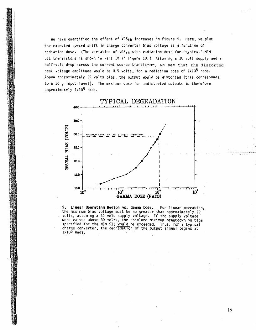
We have quantified the effect of VGSth increases 1n Figure 9 Here we plot
the expected upward shift in charge converter bias voltage as a function of radiation dose (The variation of VGSth with radiation dose for typical MEM 511 transistors is shown in Part IV in figure 10) Assuming a 30 volt supply and a half-volt drop across the current source transistor we see that the distorted peak voltage amplitude would be 05 volts for a radiation dose of 1x10⁵ rads Above approximately 29 volts bias the output would be distorted (this corresponds to a 30 g input level) The maximum dose for undistorted outputs is therefore approximately 1xl05 rads
TYPICAL DEGRADATION
S6O - I
~ I
I 0 KlO MAXIMUM LEVEL OF UNDISTORTED OPERA~ JON
gt -------------en -lt 260 In ~
~ 2OD
lt0 N
W)
100 10 10middot 10 10middot
GAlOLA DOSE (RADS)
9 linear Operating Region vs Gamma Dose For linear operation the maximum bias voltage must be no greater than approximately 29 volts assuming a 30 volt supply voltage If the supply voltage were raised above 30 volts the absolute maximum breakdown voltage specified for the MEM 511 would be exceeded Thus for a typical charge converter the degradation of the output signal begins at lxl05 Rads
19
ITENTION~LL~ LEFT BL~K
IV FAILURE MODE AND RADIATION DOSE
The Siliconix MEM 511 is a p-channel enhancement mode MOS field effect transistor designed for small signal amplifier applications As with all non-hardened MOS transistors the MEM 511 is sensitive to total radiation dose and in fact we have determined radiation dose to be the cause of degradation of YM-AMP-7025 and YM-AMP-7023 The effect of radiation (gamma radiation in this case) is to cause an increase in the gate-to-source threshold voltage VGSth of the MOS transistor The MEM 511 data sheet given in Appendix C specifies a VGSth of nominally -45 volts The VGSth voltages measured for 02 of YM-AMP-7025 and YM-AMP-7023 were -1146 volts and -892 volts respectively (measured at 10 = -10uA and VOS = -12 volts) Using these values we estimate th~ total gamma doses received by YM-AMP-7025 and YM-AMP-7023 to be 54x105 Rads and 18x105 Rads respectively
A Failure Mechanism
In a p-channel enhancement mode transistor a negative bias is nori1dlly applied
between dra in and sou rce Ora in current will flow provi ded that a I arge enough negative voltage is applied to the gate A negative voltage exceeding a certain
threshold (VGSth) between the gate and substrate converts the normally n-type substrate material directly under the gate into p-type This happens because the
electric field produced between gate and substrate draws minority carrier holes to the surface interface with the gate oxide
The gate electrode is separated from the substrate by a thin insulating layer of
Si02 (gate oxide) Gamma irradiation creates hole-electron pairs in this gate oxide Electrons being more mobile are rapidly swept out of the region by the application of a bias leaving trapped positive charge in the lattice In order for the substrate region under the gate to be converted additional negative voltage must be applied to the gate Thus the gate-to-source threshold voltage VGSth increases with radition dose
B Total Dose
Reports would indicate that shifts in VGSth cannot be used to determine radiation total dose accurately because of damage annealing - even at room temperature S We have conducted experiments to characterize annealing and have concluded that for the accuracies required here we can account for annealing
bull
21
I 1 ~
22
effects and still estimate the total gamma dose received by the device In the laboratory we exposed 5 MEM 511 transistors to gamma radiation from a 60Co source and measured the resulting VGSth as a function of dose These data are plotted in Figure 10 Each transistor was b1ased dur1ng gamma exposure since it is felt that the majority of radiation damage at TMI-2 occurred when the charge converters were biased The bias circuit used 1s shown in Appendix D This circuit is similar to that of the charge converter and its external constant current bias circuit even including the aspect that as the threshold voltage of the MEM 511 increases after irradiation the bias or compliance voltage increases
Unfortunately Figure 10 cannot be used directly to estimate the radiation total dose received because the annealing characteristics of the device must be taken into consideration For an MOS transistor it is possible to anneal out practically all gamma induced damage by thermally baking the device 8 A combination of temperature and time will supposedly through excitation of the trapped holes in the gate oxide eventually rid the gate oxide of that charge 7he problem is to first determine the temperature and time dependence and then estimate the amount of annealing which occurred before we were able to finally measure the threshold voltages of the chcrge converter transistors To do this we conducted an experiment where we baked 4 devices biased as in Figure 11 and 4 devices passively at temperatures of 500C and 70oe The transistors were baked at 500 C for 287 hours and then at 700C for an additional 1573 hours Measurements of VGSth were made at various intervals The result is shown in Figure 12 For each temperature case the threshold voltage decreases rapidly at first and then flattens out to some reasonably constant steady-state value It appears that a certain amount of damage is annealed in the first few hundred hours at a gi ven temperature and then aftert hat a very slow annea 1 i ng process takes place We have further evidence of this threshold stabilization Table 2 shows long term data we collected on the transistors used to generate Figure 10
VGSth VGSth TIME BETWEEN MEASUREMENTS lIHTIAL FINAL (lNITlAt TO FINAL)
MEM 511 TRANSISTORS [-Vl I-Vl (days)
5 TRANSISTORS EXPOSED TO 5xl05 R (AVERAGE) 1379 1181 323
3 TRANSISTORS EXPOSED Te 2xl05 R (AVERAGE) 1318 1238 280
QZ OF IM-AMP-7023 892 892 242
Q2 OF IM-AMP-7025 1146 1146 242
T_E 2 ItOON TElftRATUIIE _lUNG
-Zl
~ 0 gt L cI I 0
~ Zl ~ gt
MEM 511 VGS THRESHOLD SH I FT 180
INITIAL VGSth
14J) Ux bull 482V
Min - 362V
Mean - 429V
120
100
ao
ao ~ MAX DEVICE
0 o AVERAGE OF )
C MIN DEVICE
20
101 10middot 10 GAMMA DOSE (RADS)
10 VGSth Shift nth Gaa Dose Five MEM 511 transistors (SN 21 through 25) were exposed in steps to a 60Co source VGSth was measured at a drain current of 10 microamperes The upper curve is the maximum device tested etc These curves do not account for annealing
-CIl
tl 0 gt--Q
lt5 == I ~ gt
-1~
-1-0
-1U
-130
-125
-~
115
MEM 511 ANNEALING or bull sOe bull
SN 1 thru 4 Biaed T bull 10C -
-0-0 __ - ______ _
II
~- --- _- _---
--------VGSth wed at IC bull l~~A P~ev1ou expoaure bull SxiO R
11 ME 511 Annealing Characteristics Eight MEM 511 transistors whi ch had previ ous ly been exposed to 5x10⁵ R were anne a 1 ed at first 50degC and then at 70degC Notice the ea~ly rapid decrease in threshold voltage and then a leveling out thereafter at each temperature No particular significance is attached to the fact that the passive devices annealed further than the active ones bull (The step decreases at 219 and 287 hours are bel i eved to be measureshyment errors incurred possibly during computer reca11brat1on)
23
24
The~e transistors were stored at room temperature for hundreds of days and only minor changes in VGSth occurred Interestingly ne i middot Ier TMI transistor VGSth changed during the 242 days between our first to last measurements We can speculate that trapped charges from deeper and deeper in the oxide layer are released as the temperature is increased Eventually possibly all the damage will be annealed however for the times and temperatures of interest here long-term annealing is not a significant factor
To make our total dose estimates we assume that at TMI-2 annealing took place 1n a state of bias dur1ng the first few hundred hours after the accident at a temperature of 50degC For the next two years until we measured them they annealed passively to their present states Figure 10 is essentially the unannealed case since measurements were made a1most directly after exposure to the 60Co source Using the appropriate curves of Figure 11 and the pass veval ues from Table 2 along with Fi gure 10 we estimate that the gamma doses recei ved were approximately as shown below
TOTAL Dose Range (xl05 R) Device MIN NOM MAX
YM-AMP-7023 12 18 30 YM-AMP-702S 27 54 85
Y COMMENT
To summarize the Model 2652 appears to be well designed for non-nuclear environments however the circuit sensitivity to radiation generally makes it unsuitable for use in nuclear applications The charge converter is not designed to be radiation tolerant nor does the manufacturer Endevco claim it to be Unfortunately the device was used in an application where it shouldnt have been Perhaps the problem and its solution lie in the area of the LPM system design
We feel that US Nuclear Regulatory Guide 1133 adequately states the usefulshyness of loose parts monitoring systems in that these systems allow plant operators to avoid or mitigate accidents We believe that the Guide does not go far enough however in specifying radiation survival levels As a minimum the LPM system should survive a small LOCA such as that at TMI-2 This particular Endevco charge converter could probably be made to easily withstand a TMI-2 accident by replacing the MEM 511 transistor with a suitable bipolar transistor and adjusting component values to accommodate it The use of an MOS transistor in this particular charge converter automatically limits its usefulnes3 in a radiation environment In this case care must be taken to avoid failure simply because of the normal background radiation levels in an operating plant In fact operators of plants where this or similar charge converters are used should measure charge converter bias voltages to determine if degradation may have occurred We recommend that Regulatory Guide 1133 be changed to help prevent this in future designs and that existing plants replace these (and similar) charge converters with more radiation tolerant ones
bull
25
I
26
Appendix A Unit 2 lOS Elevation Floor Plan
The approx1mate 10cat10ns of the two remote charge converters used 1n the loose parts mon1tor system 1n Un1t 2 are shown above tn the 305 elevat10n plan v1ew
I Appendix B Outline Drlwing of the Endevco ~te Charge Converter
amp--
I 87sect evA Rfr
N01pound
1 N LASH 1011 ACE 01 IJNIT) TO 13pound APFLlEt) IV IU~ rc I r ~ 1A1REMil OF UNIT) As sHOWN
7
lt A- SEMBLE n 5 r 8 IfiSECT PER OS TflltVELpoundR IUSS -511$
L I middotWIEFmiddot ~s l~rgt4pound Amiddot4 poundmiddotto amp Uff 10 d~ J Ntf MI~ IUE IJr TIIMIIIl ~IIIDJ
1 Lvf IflM AI r LpoundNrItWI~1(Y6MIN WIOTH)sPt----- il CQVA PAltpoundD IMf)MLLr TO ALLOW orriNe MArpoundttIAL TO
FlU rtlfltI
il 1 j
(1VON-IHSulltTEO TERMINAL)
The standard output terminals shown in the draw1ng may be replaced with an optional
SNC type connector Both YM AMP 7023 and YMAMP 7025 had the BNC type output
connector
27
I I 1 i
28
Appendix C Manufacturers Specification listing for the MEM 511
M511 511A P-CHANNEl ENHANCEMENT -TYPE MOS SILICON FIELDmiddot EFFECT TRANSISTOR
bull Integrated Zener Clamp Protect the Oate
PRODUCT CONDITIONING
t
TO-12 Bod Cu conneded lntemail
Unitll recelve the followlq treatment before nul electrlcll test
High Temp Storage 24 Hoore at 150middotC 25000 AcceleraUonImpact in the Y1 Plane Thennll Shock +100 to OC for 5 Cyclell HeBum andor OroSI Leak Test forHennetlclty
ABSOLUTE MAXIMUM RATINGS (25C)
Drain-to-SOlirce Voltage bullbullbullbullbullbullbullbullbullbullbullbullbullbullbullbullbullbullbullbullbullbullbullbullbullbullbullbullbullbullbullbullbullbullbullbullbullbullbullbullbullbullbullbullbullbullbull Oate-to-Source Voltage bullbullbullbullbullbullbullbullbullbullbullbullbullbullbullbullbullbullbullbullbullbullbullbullbull _ bullbullbullbullbullbullbullbullbullbullbullbullbullbullbullbullbullbull Oate-to4Drain Voltage bullbullbullbullbullbullbullbullbullbullbullbullbullbullbullbullbullbullbullbullbullbullbullbullbullbullbullbullbullbullbullbullbullbullbullbullbullbullbullbullbullbullbullbullbullbullbullbullbull Drain Current ahte Current (Forward DIrection for Zener Clamp) bullbullbullbullbullbullbullbullbullbullbullbullbullbullbullbullbullbullbullbullbullbullbull
-30 V -30 V -30 V
-50 rnA +01 rnA
SlaquoJrage Temperature f bullbullbullbullbull bull bull bull bullbullbullbullbull bullbullbull -65 to 150degC Operating JuncUon Temperalure bullbullbullbullbullbullbullbull bullbullbullbullbullbullbullbullbullbullbullbullbullbullbullbullbullbullbullbullbullbull bullbullbullbullbull -55 to 125degC Totll DlllllpaUon at 25degC Amblent Temperature (Derate 225 mWee) bullbullbull bull bullbullbull bullbull bull 225 mW
ELECTRICAL CHARACTERISTICS
win nBA I
c t1 to e I)nI 011 tIl bullbull t 101 11 YI 101 -I ~ bullbullbullbull 0
ye o nHtIItampcYoI YOI 01 lb 10_A v bullbullbullbull - J --IY Dna Vol IOmiddotmiddotIOM GIO V - _DrNi YolaCt t- middotIO_A Vao 0 Vb Q vOIbull O_~1kMt1 Vo1-1 0 -to JtA VII - G YDI bull 0 - to middotto y
nt CIU II 14tQ 0 Val YDI bull -itv vo- yo M
I (1ft- 119 yenIIDmiddot middot1 V YOb 0 Yomiddot middot1 bull C-- -0 a Ikl4fL vomiddot -IV VDI v -10 ~LO 1lIOIltgt OnlaCu-middot Ill- middot10Y v(I middottOV v 0 - J
VDII bull -I I r=1 lt - _eN tr -bullbull r--It YOImiddot 11 I V_ 1- tMM - -
C G_~ C_i-- YuIIlYnmiddot v bullbull t MMI bull bull I
CoO a O c l- Od I---- U c c_t ___
Vou yentampY SV I c nnllt~ c_n I MM f-- U c O c_ 0middot bullbull vDmiddot A - lV
middotIIh O U 1 r
- t 1 IIIA MI
NIIIIIri - _t ~
APPENDIX D MEM 511 BIAS CIRCUIT
The circuit shown below was used to bias MEM 511 transistors being irradiated in steps to estimate the gamma dose received by TMI-2 MEM 511 transistors The circuit simulates the changing bias condition of the TMI-2 device The select resistor (approximately 45Kn) is initially adjusted to produce a 12 volt bias on the MEM 511 The constant current source initially supplies approximately 300~A to the MEM 511 being exposed to gamma radiation
501(
lt
29
30
REFERENCES
1 J E Jones J T Smith M V Mathis GEND-INF-0l7 January 1982 Field Measurements and Interpretation of TMI-2 Instrumentation YM-AMP-7023 and
YM-AMP-7025
2 Catalog of TMI-2 Data Proposal 80-78 Babcock and Wl1cox 30 October 1980
File 80-78
3 Allen Morris Tennessee Valley Authority Personal Communication
4 Regulatory Guide 1133 May 1981 Rev I US Nuclear Regulatory Commission
5 John Brummer General Public Utilities Personal Communication
6 Endevco Instruction Manual Model 447912652 Remote Charge Converter and
Conditioner Mode Card dtd 871
7 Sandia Laboratory Notebook ENG-F-780 L G Pickard 1981
8 George C Messenger Radiation Effects Short Course Sandia National Laboratories Spri ng 1981 cl ass notesmiddotmiddot
J
ABSTRACT
During and for several months after the Three Mile Island Unit 2 accident the reactor vessel and two steam g~nerators were closely monitored for the existence of coolant system loose parts We have examined two Endevco charge converters removed from the loose parts monitoring system inside containment and found the devices to be severely degraded by gall11la radiation Because of this it is likely that the loose parts readings made during the accident were lower than actual levels This report discusses the cause of failure our estimates of the total gamma radiation doses received by the charge converters and our recommendations for changes 1n US Nuclear Regulatory Guide 1133
3
middot_-__----bull -
CONTENTS
I INTRODUCTION AND SUMMARY FINDINGS A Findings and Recommendations
II DESCRIPTIOM A Rockwell lPM System at TMI-2
B Operational History
C Charge Converter Mechanical Descrfption
D Charge Converter Functional Description
III ELECTRICAL EVALUATION A Test Sequence
B Evaluation of YM-AMP-7025
C Evaluation of YM-AMP-7023
D Effect of Degradationon Circuit Operation
IV FAILURE MODE AND RADIATION DOSE A Failure Mechanism
B Total Dose
v COfIiIENT
7
9
10
10
11
14
14
17
18
21
21
25
APPENDIX A Unit 2 305 Elevation Floor Plan 26
APPENDIX B Outli neDrawing of Eridevco Remote Charge Converter 27
APPENDIX C Manufacturers Specification Listing for the HEM 511 28
3 Charge ConverterSchemaHc 4 Model 4479~ 1 Line Driver Condit1oner Schematic 5 Endevco Model 2652 Test Set-up 6 YM-AMP-7025 Osc1lloscope Trac1ngs 7 YM-AMP-7025 Transfer Characterist1c 8 YM-AMP-7023 Transfer Characterist1c 9 linear Operat1ng Region vs Gamma Dose 10 VGSth Shift with Gamma Dose 11 MEM 511 Annealing Character1stics
Tables
1 DC Operating Point Measurements 2 Room Temperature Anrieali ng
9
11
13
13
14
15
15
17
19
23
23
16
22
I INTRODUCTION AND SUMMARY FINDINGS
This report contains the results of our laboratory examinations of two Endevco Model 2652M4 Remote Charge Converters which were removed from the Three Mile Island Unit 2 (TMI-2) conta1nment building in November 1980 In situ testing done in ~ptember 1980 indicated that both charge converters h~ving TMI-2 tag numbers YM-AMP-7023 and YM-AMP-7025 were inoperable at the t1me of the measureshyments 1 Records obtained in the accident time frame indicate that all eight Rockwell steam generator loose parts monitoring (LPM) channels each containing Endevco charge converters may have failed or were close to failure during the first few days of the TMI-2 accident 23 This is ind1cated by the need on April 2 1979 to increase channel gains and a few weeks later the measurement of inappropriately high bias voltages
The charge converters were mounted inside protective boxes on t~e outside of the 0 ring wall on the 305 foot elevation near the personnel hatch of the TMI-2 containment build1ng (see Appendix A) They were removed for laboratory examination because they had failed they contain radiat10n sensitive HDS trans1stors known to be useful as radiation dosimeters and they were l~a5ily
accessible bull This report is not meant to evaluate the entire LPM system Here we discuss the cause of failure of the charge converters and the implications of this on loose parts monitoring We also make est1mates of the total gamma radiation doses recei ved by each charge converte r ~
-A Findings and Recommendations
1 Both charge converters wJr~ d~graded by ~adiation probably in the first few days of the accident to th~middot extent that YM-AMP-7025 was non-funttional ~~d YM-AMP-7023 was marginally funtt1orlaT The degradation 1n both ases wasmiddot caused by a large upward sh1ft in the gate-to-source threshold voltage of the MEM 511 transistor used 1n the Q2 slot This can result 1n an indication of lower vibration levels than are actually there The MEM 511 is an MOS f1eld effect tranSistor and like all non-hardened I()S transistors it is quite sens1t1ve to rad1at10n dose Our tests 1nd1cate that because uf this tranSistor these charge converters are usable up to only approdmately bIOS rads
2 The fa1lure mode observed in these charge converters 1s espeCially 1ns1d10us since the LPM channel can appear to operate properly even a ftef severe
7
8
degradation has occurred The only normal indication of this condition is that the usual background vibration levels would appear to decrease Fortunately the condition can be detected remotely by measuring the charge converter DC bias voltage and looking for a higher than normal level The normal bias voltage 1s about 135 volts This voltage will shift upwards as radiation dose is accumulated until in the limit the power supply rail (normally 30 volts) is reached We recommend that all power plant operators using this and similar model Endevco charge converters perform the above measurements to determine the state-of-health of their LPM systems This same problem has been observed in operat1ng plants where the charge converters are located in high rad1at10n fields 3
3 We recommend that Endevco Model 2652M4 charge converters other s1mllar Endevco models and other manufacturers models which cannot survive low radiation exposure be removed from nuclear power plants and replaced with more radiation tolerant designs MOS transistors should not be used in any appl lCyti~n where inherent or potential radiation exposure is possible
4 We recommend that U S Nuclear Regulatory Guide 1133 be modified to strongly encourage the use of radiation resistant LPM systems The May 1981 Revision 1 guide states Early detectiol) (of loose parts) can provide the time requi red to avoid or mitigate safetgt-related damage to ormaHunctions of primary system components4 This statement is actually relevant fora power plant operating normally as well as during an acciderit During an accident where operators do not have access to the containment building the LPM system can potentially provide a much needed indication of vibration andor impact levels Operators can use this information to possibly m1tigate further damage The Guide should specify design goal radiation levels which are consistent with those required for Class IE equipment
5 The degradation in VGS(th) of the MOS transistors indicates that YM-AMP-7023 and YM-AMP-7025 received toUl gamma doses of 18xl0S and 54xlOS Rads respectively These levels correlate well with the estimate of 2SxlOS rads received by radiation detector HP-R-211 located near-by
-----------------------_
II DESCRIPTION
A Rockwell lPM System at TMI-2
The Rockwell lPM System at TMI-2 uses a total of eight channels to monitor
the upper and lower tube sheets of the two steam generators Signals from these channels are processed 1n a Rockwell electronics cabinet located in the cable
spreading room Alarms and a channel selectable audio output are located in the control room Each channel consists of an Endevco Model 2276 accelerometer mountshy
ed on the tube sheet and an Endevco Model 2652M4 charge converter mounted outside the O-ring A photograph of the charge converter is shown in Figure 1 The accel- erometers are exposed to high temperatures and radi at ion while the charge con verters are in much 1 ess severe envi ronments The norma 1 rad i at i on fie 1 d a round
the charge converters is on the order of 1 to 10 mRadhr YM-AMP-7023 and YM-AMP-7025 a re used to mon i tor oppos i te sides of steam generator B upper tube sheets The$e are connected to the Rockwell cabinet by approximately 110 meters and 200 meters of coaxial cable respectively
1 YM-AMP-1025 ~te Charge Con~erter Actual size is 57 cm x 222 em Signal input connector shown
9
I
10
B Operational History
We have not attempted to piece together a precise operational history of the LPM channels however we will provide a sketch of information given to us 235 The LPM system as described above was calibrated and operational at the time of the accident The day after the accident a team of Babcock and Wilcox (BampW) technicians were dispatched to TMI-2 to monitor and record the LPM outputs They replaced the Rockwell readout system with a BampW system having a magnetic tape recorder and various filters and signal conditioning electronics The channels were monitored quite closely during the first week following the accident and then at least daily for the remainder of April 1979 The channels were then monitored periodically for several months During the month-long vigil most of the channels were believed at the time to be functional ie normal sounds were heard At the time in situ testing on YM-AMP-7023 and YM-AMP-7025 was done we were informed by GPU that 7 of 8 channels were inoperable Indeed the in situ data show both YM-AMP-7023 and YM-AMP-7025 to be severely degraded or inoperable (see Section III )
On reviewing the information we have it appears that most of the channels had severe degradation within a day or days after theacciClent began This is indicated by the need to adjust the bias levels to 100 It appears that this was necessary the day after the accident began although we know of no written records of this Several weeks after the accident these bias levels were recorded and all were near 100 Another indicator of degradation was the need by BampW to increase channel gains on April 1 and 2 1979
C Charge Converter Mechanical Description
The Endevco Model 2652M4 charge converter is shown disassembled in Figure Z This particular unit is YM-AMP-7025 The electronic circuitry is potted and housed inside a metal tubular case 4~ cm long and 19 cm in diameter The case is actually an outer housing over an inner shield housing with the two being electrically isolated from each other The Microdot(R) connector and BNC connector are electrically grounded to the inner shield case An outline drawing is given in Appendix B
2 Disassembled Remote Charge Converter The double shield is used to provide extra isolation from electromagnetic interference
D Charge Converter Functional Description
The funct i on perfotmed by the Mode I 2652 cha rge converter is the con velS i on of an electrical charge generated by a piezoelectric transducer into a voltage proportional to the input acceleration (shock or vibration)~ This voltage is then supplied to a remote readout calibrated in gs to Indicate the vibration level The Model 2652 is usually located in close proximity to the transducer and is designed to drive long coaxial cables which are used to interconnect the read-out The M4 version of the Model 2652 has a conversion gain of 1 millivolt per picocoulomb The remote readout has selectable peak acceleration ranges of Olg 03g LOg 30g 109 and 30g
11
12
Figure 3 shows a schematic of the charge converter The output line serves both to supply DC power to the device and to carry the AC output signal to the remote readout The circu1t conststs of a very high tnput impedance input amplifier (Ql) a second amplifier (Q2) and a low output impedance line driver (03) In operation the output AC voltage which occurs as a result of the charge Input signal is fed back to the input via CI The polar1ty 15 such as to ma1ntain the voltage at the 1nput near zero Th1s means that the Input charge is stored on
capacitor CI and thus the output voltage eo(t) is given by
eo(t) bull - - q(t) CI
Where q(t) is the Input charge The advantage of this feedback arrangement is to effectively swamp out input cable capacitance vcriations w1th a large capacitor The circuit gain of this particular circuit 15
Eo bull I bull 1 bull Imv Q TI lOOOpf pc
The 2652M4 is biased with the constant current source 01 shown 1n F1gure 4 Th1s circu1t nominally drives the 2652M4 with 8 milliamperes DC The DC compliance voltage 15 set by selection of R6 1n Figure 3 and is nominally 135 volts Resistor
R6 is used to adjust the drain current of 01 so that the voltage drop across RS is sufficient to overcome the gate-to-source threshold voltage (VGSth) of transistor 02 The threshold volt~ge of th MEM 511 is nominally -45 volts Since the circuit is being dr1ven by a curt-ent source the DC voltage (compliance Voltage) appearing across the circuit from output to ground (Pin 2 to Pin 3) will rise until the circuit does in fact draw 8 mil11amperes Th1s happens because an increase In the b1as ~oltage t~nds to turn 02 on harder and more base current Is suppl1ed to Q3 causing 1t to sink the requi red 8 milliamperes This method of neglit ive DC feedback is normally very good in stabiliz1ng the operating points of the three transistors against 1uiat10ns in temperature and component parameters As we will see later the increase in VGSth of Q2 caused by radiation results in the need for the compliance voltage to rise 1n order to keep Q2 on
bull bull bull
I I
I I -Ll II
INPuT I I RI I t IKM
tlOl a4 I I kC RI I I 3 INlt4S 3 1 I 1 _____________ L __________ I I I 1 _________________________ ---I
$IGNAl GAD
__ ___ ~~ _______ --- _____ -J __
3 Charge Converter Schemat1c The ope rat 1 ng poi nt measureshyments in Table were made at thr points indicated by letters ABC D Q2 an MEM 511 MOS transistor was found to be degraded by radiation
QI
4 Model 44191 Une Drher Conditioner Sch_tic Trans1stor Q1 is configured as a constant current generator providing the bias current to the Remote C~arge Converter through pin 12 of the connector
13
14
III ELECTRICAl EVAlUATION
In th1s sect10n we descr1be the electr1cal evaluations performed on YM-AMP-7025 and YM-AMP-7023 and d1scuss the cause of degradation or fa1lure We found that YM-AMP-7025 was completely non-operational and YM-AMP-7023 had output d1stortion for acceleration levels in excess of 19 The cause of fa1lure was found to be radiat10n degradat10n of the MEM 511 MOS transistor used in the 02 slot
A Test Sequence
Both YM-AMP-7025 and YM-AMP-7023 charge converters (Endevco SN ZB47 and ZB50) were found to be slightly contaminated upon arrival from Three Mile Island Each was carefully scrubbed using alcohol before any electrical tests were done and care was taken to avoid getting alcohol inside the Microdot or BNC connectors After decontamination the two devices were taken to the laboratory for the electrical examination Each underwent passive and powered testing before d1section and troubleshooting The passive and powered in situ tests performed at TMI-2 indicated normal resistance and capacitance values but abnormal bias currents and voltages There was no AC output from YM-AMP-7025 Our examination verified the in situ measurements and provided additional data because we could use a calibrated input stimulus
B Evaluation of YM-AMP-7025
Electrical evaluation of the Model 2652 requires a charge generator to provide a~ input signal and a DC source to provide power The test set-up shown in Figure 5 was used for testing as it is recommended by the manufacturer for 2652 operational checkout A schematic of the Endevco 44791 signal conditioner used is shown in Figure 4
0 bullbull 11 1000111
ff4rmiddotl--~I+-I~ bullbullbull j
---_
5 Model 2652 Set-up This set-up is identical to that recommended by Endevco except that the Charge Conshyverter output is monitored instead of the 44791 output 6
(a) (b)
6 YM-AMP-7025 Osci11oscopeTracings These actual photographs of the Charge Converter input and output signals illustrate the non-linear operating mode of YM-AMP-7025 The waveforms shown in (a) are for an input level (lower trace) equivalent to 13 gs peak For this input signal the output (upper trace) would indishycate about 01g peak Tracing (b) shows an equivalent input level of 20gs peak and the distorted output indicating perhaps 25g peak
Initial AC measurements were made using a 1 kilohertz variable amplitude source We found that the charge converter output was essentially zero until quite large input signals were applied Even then the output was severely attenuated and distorted The output positive going portion of the sine wave was found to be more attenuated than the negative going portion This is shown in the oscilloscope pictures in Figure 6 Figure 7 shows a plot of the AC voltage transfer characteristic where the amplitudes of the positive peaks and negative peaks are plotted for various input peak voltages The amplitude of the negative gOing port i on of the output signal is on 1y correct at hi gh signa ~ 1 eve 1 s The amp 1 itude of the positive going portion is always attenuated At this point the unit was disected so that the DC operating points could be determined 10o~---L~~~~~--~~~~~~--~--~~~~
shy
IOlA~t
shy
-
NEGAH VE PfAKS __ PO I TVE PEAK
7 YM-AMP-7025 Transfer Character-1stics The charge amp 11fi er output peak magnitude is plotted versus input peak amplitude The ideal and post reshypair characteristic is shown dotted With the degraded trans stor both positive going peaks and negative going peaks are attenushyated Equivalent input g levels are also shown
15
Hi
The Model 2652 is housed in a double shielded metal enclosure and requires the use of a cutting disc to remove the case shield The unit was potted in an amber epoxy compound which was easily spot-removed by applying heat and crumbling with a soldering iron Points of interest were exposed in this manner These points are shown on the circuit schematic as ABC and O DC voltages were measured at these points and at the output 7 Also the DC input current into pin 2 was measured The recorded values are shown in Table 1 under the heading YM-AMP-7025 pre-repair
VOLTAGE at A 4399 VOLTS 1722 VOLTS 4297 VOLTS 1 712 VOLTS
VOLTAGE at B 2025 VOLTS 6871 VOLTS 1910 VOLTS 6808 VOLTS
VOLTAGE at C 0156 VOLTS 1585 VOLTS 1385 YOLfS 1634 VOL T5
VOLTAGE at 0 5085 VOLTS 2514 VOLTS 4711 VOLTS 2273 VOLTS
VOLTAGE at 2 -ltOutput Bias) 2926 VOLTS 1142 VOLTS 2872 VOLTS 1143 VOLTS
CURRENT into 2 (I nput Current) 0484 mAmps 788 mAmps 2amp0 mAmps 784 mAmps
TAlltE 1 DC OPEIlATlIIG POlIO IIASUREIIIITS
Analysis of the DC measurements indicated that a shift in the DC operating pOint had occurred The output bias (voltage at pin 2) had shifted upward to 2928 volts from a nominal value of 135 volts and the input current had decreased to 0484 milliamperes from a nominal 80 milliamperes The voltage at point C was insuff1cient to b1as Q3 on (lion being operational) explaining the low input current and high output DC voltage Also the c11pp1ng of AC output signals was easily explained as Q3 would require a relatively large positive 1nput to produce an output Measurements at points AB and D ind1cated that Q2 had failed The voltage at p01nt B was suff1cient to overcome the normal threshold voltage of Q2 and b1as it on This should in turn bias Q3 at a suitable operating point 42 an HEM 511 MaS field effect transistor was removed for failurJ analysis and was found to have an out-of-spec VGSth The specified range of VGSth for a normal MEM 511 device is from -3 to -6 volts (Append~x C)
The performance of the converter was restored to within specification limits by the replacement of Q2 Post repair AC and DC measurements are shown in Figure 7 and Table I respectively for comparison with the pre-repair data The output bias voltage decreased to 1142 volts and the input current 1ncreased to 7886 m1lliamperes These are both near nom1nal levels The select resistor R6 could probably be adjusted so that the output bias voltage and input current approached the nominal values of 135 volts and 80 milliamperes
C Evaluat10n of YM-AMP-7023
YM-AMP-7023 was evaluated us1ng methods identical to those used on YM-AMP-7025 The AC voltage transfer characteristic obtained is shown In Figure 8 The output was free from d1stortlon and attenuat10n for low s1gna1 levels but was slightly distorted at higher levels The charge converter operated properly for Input levels up to Ig on the Endevco system Negative input signals above th1s level produced outputs which were slightly attenuated due to the same clipping act10n exhibited by YM-AMP-7025 Positive input signals produced unattenuated outputs beyond the maximum 30g equ1valent input level Voltages at points ABCD pin 2 and the Input current Into p1n 2 were measured after all points were exposed The recorded values are l1sted 1n Table 1 und~r the head1ng DC pt1easurements YM-AMP-7023 pre-repair
10~----~~~~~----~--~~~~----~-L~~~
NEGA TI VI PIAU (lDIAL)
10
8 YM-AMP~7023 Transfer Characteristic Unlike YM-AMP-7025 the negat1ve g01ng peaks are unattenuated Only a slight attenuation is seen for positive going peaks
17
18
Analysis of the DC measurements indicate a DC operating pOint shift similar to the shift in YM-AMP-7025 The output bias voltage increased to 2872 volts and the input current decreased to 28 milliamperes The voltage at pOint C however was sufficient to keep Q3 biased slightly on for low signal levelsaccounting for the difference in input currents between YM-AMP-7023 and YM-AMP-7025 The voltages at operating points AB and D indicate that Q2 was operating at an incorrect bias point Specifically the voltage measured at point B was more than adequate to insure strong bias of the Q2 and Q3 stages Q2 was removed for failure analysis and found also to have an abnormally high VGSth
D Effect of Degradation on Circuit Operation
The effect of a gradual increase in the VGSth of Q2 as radiation dose is accumulated is to cause a proportional increase in the charge converter bias voltage This happens because the transistor DC operating pOints are stabilized by the control loop described earlier As the threshold voltage of Q2 increases the available drive to Q3 is reduced causing the bias voltage (pin 2) to incrt~se This in turn provides Q2 with a higher gate-to-source voltage and the drive to Q3 increases This give and take can continue until it is limited by the recommended 30 volt DC supply As the bias voltage nears 30 volts large output signals become distorted as shown in Figure 6 As the bias voltage continues to approach the 30 volt sup~ly proportionally lower levels will become distorted This limit nominally 29 volts is the point where Q2 cuts off and can no longer provide bias to Q3
Positive input levels of sufficient magnitude may overcome this limit by indirectly providing bias to Q3 These inputs however produce attenuated outputs The input level required to overcome this threshold continues to increase with increasing Q2 threshold voltage for all practical inputs The limit approached here is not meaningful as it would exceed the recommended operating range of the converter The converter could also be made to operate simply by increasing the bias voltage were it not for the MEM 511 maximum rated drain to source breakdown voltage of -30 volts To summarize as dose is accumulated the first effect seen is that large output signals resulting from large amplitude vibrations become distorted When enough dose is accumulated small vibrations will not be measured and large ones will be severely attenuated
We have quantified the effect of VGSth increases 1n Figure 9 Here we plot
the expected upward shift in charge converter bias voltage as a function of radiation dose (The variation of VGSth with radiation dose for typical MEM 511 transistors is shown in Part IV in figure 10) Assuming a 30 volt supply and a half-volt drop across the current source transistor we see that the distorted peak voltage amplitude would be 05 volts for a radiation dose of 1x10⁵ rads Above approximately 29 volts bias the output would be distorted (this corresponds to a 30 g input level) The maximum dose for undistorted outputs is therefore approximately 1xl05 rads
TYPICAL DEGRADATION
S6O - I
~ I
I 0 KlO MAXIMUM LEVEL OF UNDISTORTED OPERA~ JON
gt -------------en -lt 260 In ~
~ 2OD
lt0 N
W)
100 10 10middot 10 10middot
GAlOLA DOSE (RADS)
9 linear Operating Region vs Gamma Dose For linear operation the maximum bias voltage must be no greater than approximately 29 volts assuming a 30 volt supply voltage If the supply voltage were raised above 30 volts the absolute maximum breakdown voltage specified for the MEM 511 would be exceeded Thus for a typical charge converter the degradation of the output signal begins at lxl05 Rads
19
ITENTION~LL~ LEFT BL~K
IV FAILURE MODE AND RADIATION DOSE
The Siliconix MEM 511 is a p-channel enhancement mode MOS field effect transistor designed for small signal amplifier applications As with all non-hardened MOS transistors the MEM 511 is sensitive to total radiation dose and in fact we have determined radiation dose to be the cause of degradation of YM-AMP-7025 and YM-AMP-7023 The effect of radiation (gamma radiation in this case) is to cause an increase in the gate-to-source threshold voltage VGSth of the MOS transistor The MEM 511 data sheet given in Appendix C specifies a VGSth of nominally -45 volts The VGSth voltages measured for 02 of YM-AMP-7025 and YM-AMP-7023 were -1146 volts and -892 volts respectively (measured at 10 = -10uA and VOS = -12 volts) Using these values we estimate th~ total gamma doses received by YM-AMP-7025 and YM-AMP-7023 to be 54x105 Rads and 18x105 Rads respectively
A Failure Mechanism
In a p-channel enhancement mode transistor a negative bias is nori1dlly applied
between dra in and sou rce Ora in current will flow provi ded that a I arge enough negative voltage is applied to the gate A negative voltage exceeding a certain
threshold (VGSth) between the gate and substrate converts the normally n-type substrate material directly under the gate into p-type This happens because the
electric field produced between gate and substrate draws minority carrier holes to the surface interface with the gate oxide
The gate electrode is separated from the substrate by a thin insulating layer of
Si02 (gate oxide) Gamma irradiation creates hole-electron pairs in this gate oxide Electrons being more mobile are rapidly swept out of the region by the application of a bias leaving trapped positive charge in the lattice In order for the substrate region under the gate to be converted additional negative voltage must be applied to the gate Thus the gate-to-source threshold voltage VGSth increases with radition dose
B Total Dose
Reports would indicate that shifts in VGSth cannot be used to determine radiation total dose accurately because of damage annealing - even at room temperature S We have conducted experiments to characterize annealing and have concluded that for the accuracies required here we can account for annealing
bull
21
I 1 ~
22
effects and still estimate the total gamma dose received by the device In the laboratory we exposed 5 MEM 511 transistors to gamma radiation from a 60Co source and measured the resulting VGSth as a function of dose These data are plotted in Figure 10 Each transistor was b1ased dur1ng gamma exposure since it is felt that the majority of radiation damage at TMI-2 occurred when the charge converters were biased The bias circuit used 1s shown in Appendix D This circuit is similar to that of the charge converter and its external constant current bias circuit even including the aspect that as the threshold voltage of the MEM 511 increases after irradiation the bias or compliance voltage increases
Unfortunately Figure 10 cannot be used directly to estimate the radiation total dose received because the annealing characteristics of the device must be taken into consideration For an MOS transistor it is possible to anneal out practically all gamma induced damage by thermally baking the device 8 A combination of temperature and time will supposedly through excitation of the trapped holes in the gate oxide eventually rid the gate oxide of that charge 7he problem is to first determine the temperature and time dependence and then estimate the amount of annealing which occurred before we were able to finally measure the threshold voltages of the chcrge converter transistors To do this we conducted an experiment where we baked 4 devices biased as in Figure 11 and 4 devices passively at temperatures of 500C and 70oe The transistors were baked at 500 C for 287 hours and then at 700C for an additional 1573 hours Measurements of VGSth were made at various intervals The result is shown in Figure 12 For each temperature case the threshold voltage decreases rapidly at first and then flattens out to some reasonably constant steady-state value It appears that a certain amount of damage is annealed in the first few hundred hours at a gi ven temperature and then aftert hat a very slow annea 1 i ng process takes place We have further evidence of this threshold stabilization Table 2 shows long term data we collected on the transistors used to generate Figure 10
VGSth VGSth TIME BETWEEN MEASUREMENTS lIHTIAL FINAL (lNITlAt TO FINAL)
MEM 511 TRANSISTORS [-Vl I-Vl (days)
5 TRANSISTORS EXPOSED TO 5xl05 R (AVERAGE) 1379 1181 323
3 TRANSISTORS EXPOSED Te 2xl05 R (AVERAGE) 1318 1238 280
QZ OF IM-AMP-7023 892 892 242
Q2 OF IM-AMP-7025 1146 1146 242
T_E 2 ItOON TElftRATUIIE _lUNG
-Zl
~ 0 gt L cI I 0
~ Zl ~ gt
MEM 511 VGS THRESHOLD SH I FT 180
INITIAL VGSth
14J) Ux bull 482V
Min - 362V
Mean - 429V
120
100
ao
ao ~ MAX DEVICE
0 o AVERAGE OF )
C MIN DEVICE
20
101 10middot 10 GAMMA DOSE (RADS)
10 VGSth Shift nth Gaa Dose Five MEM 511 transistors (SN 21 through 25) were exposed in steps to a 60Co source VGSth was measured at a drain current of 10 microamperes The upper curve is the maximum device tested etc These curves do not account for annealing
-CIl
tl 0 gt--Q
lt5 == I ~ gt
-1~
-1-0
-1U
-130
-125
-~
115
MEM 511 ANNEALING or bull sOe bull
SN 1 thru 4 Biaed T bull 10C -
-0-0 __ - ______ _
II
~- --- _- _---
--------VGSth wed at IC bull l~~A P~ev1ou expoaure bull SxiO R
11 ME 511 Annealing Characteristics Eight MEM 511 transistors whi ch had previ ous ly been exposed to 5x10⁵ R were anne a 1 ed at first 50degC and then at 70degC Notice the ea~ly rapid decrease in threshold voltage and then a leveling out thereafter at each temperature No particular significance is attached to the fact that the passive devices annealed further than the active ones bull (The step decreases at 219 and 287 hours are bel i eved to be measureshyment errors incurred possibly during computer reca11brat1on)
23
24
The~e transistors were stored at room temperature for hundreds of days and only minor changes in VGSth occurred Interestingly ne i middot Ier TMI transistor VGSth changed during the 242 days between our first to last measurements We can speculate that trapped charges from deeper and deeper in the oxide layer are released as the temperature is increased Eventually possibly all the damage will be annealed however for the times and temperatures of interest here long-term annealing is not a significant factor
To make our total dose estimates we assume that at TMI-2 annealing took place 1n a state of bias dur1ng the first few hundred hours after the accident at a temperature of 50degC For the next two years until we measured them they annealed passively to their present states Figure 10 is essentially the unannealed case since measurements were made a1most directly after exposure to the 60Co source Using the appropriate curves of Figure 11 and the pass veval ues from Table 2 along with Fi gure 10 we estimate that the gamma doses recei ved were approximately as shown below
TOTAL Dose Range (xl05 R) Device MIN NOM MAX
YM-AMP-7023 12 18 30 YM-AMP-702S 27 54 85
Y COMMENT
To summarize the Model 2652 appears to be well designed for non-nuclear environments however the circuit sensitivity to radiation generally makes it unsuitable for use in nuclear applications The charge converter is not designed to be radiation tolerant nor does the manufacturer Endevco claim it to be Unfortunately the device was used in an application where it shouldnt have been Perhaps the problem and its solution lie in the area of the LPM system design
We feel that US Nuclear Regulatory Guide 1133 adequately states the usefulshyness of loose parts monitoring systems in that these systems allow plant operators to avoid or mitigate accidents We believe that the Guide does not go far enough however in specifying radiation survival levels As a minimum the LPM system should survive a small LOCA such as that at TMI-2 This particular Endevco charge converter could probably be made to easily withstand a TMI-2 accident by replacing the MEM 511 transistor with a suitable bipolar transistor and adjusting component values to accommodate it The use of an MOS transistor in this particular charge converter automatically limits its usefulnes3 in a radiation environment In this case care must be taken to avoid failure simply because of the normal background radiation levels in an operating plant In fact operators of plants where this or similar charge converters are used should measure charge converter bias voltages to determine if degradation may have occurred We recommend that Regulatory Guide 1133 be changed to help prevent this in future designs and that existing plants replace these (and similar) charge converters with more radiation tolerant ones
bull
25
I
26
Appendix A Unit 2 lOS Elevation Floor Plan
The approx1mate 10cat10ns of the two remote charge converters used 1n the loose parts mon1tor system 1n Un1t 2 are shown above tn the 305 elevat10n plan v1ew
I Appendix B Outline Drlwing of the Endevco ~te Charge Converter
amp--
I 87sect evA Rfr
N01pound
1 N LASH 1011 ACE 01 IJNIT) TO 13pound APFLlEt) IV IU~ rc I r ~ 1A1REMil OF UNIT) As sHOWN
7
lt A- SEMBLE n 5 r 8 IfiSECT PER OS TflltVELpoundR IUSS -511$
L I middotWIEFmiddot ~s l~rgt4pound Amiddot4 poundmiddotto amp Uff 10 d~ J Ntf MI~ IUE IJr TIIMIIIl ~IIIDJ
1 Lvf IflM AI r LpoundNrItWI~1(Y6MIN WIOTH)sPt----- il CQVA PAltpoundD IMf)MLLr TO ALLOW orriNe MArpoundttIAL TO
FlU rtlfltI
il 1 j
(1VON-IHSulltTEO TERMINAL)
The standard output terminals shown in the draw1ng may be replaced with an optional
SNC type connector Both YM AMP 7023 and YMAMP 7025 had the BNC type output
connector
27
I I 1 i
28
Appendix C Manufacturers Specification listing for the MEM 511
M511 511A P-CHANNEl ENHANCEMENT -TYPE MOS SILICON FIELDmiddot EFFECT TRANSISTOR
bull Integrated Zener Clamp Protect the Oate
PRODUCT CONDITIONING
t
TO-12 Bod Cu conneded lntemail
Unitll recelve the followlq treatment before nul electrlcll test
High Temp Storage 24 Hoore at 150middotC 25000 AcceleraUonImpact in the Y1 Plane Thennll Shock +100 to OC for 5 Cyclell HeBum andor OroSI Leak Test forHennetlclty
ABSOLUTE MAXIMUM RATINGS (25C)
Drain-to-SOlirce Voltage bullbullbullbullbullbullbullbullbullbullbullbullbullbullbullbullbullbullbullbullbullbullbullbullbullbullbullbullbullbullbullbullbullbullbullbullbullbullbullbullbullbullbullbullbullbullbull Oate-to-Source Voltage bullbullbullbullbullbullbullbullbullbullbullbullbullbullbullbullbullbullbullbullbullbullbullbullbull _ bullbullbullbullbullbullbullbullbullbullbullbullbullbullbullbullbullbull Oate-to4Drain Voltage bullbullbullbullbullbullbullbullbullbullbullbullbullbullbullbullbullbullbullbullbullbullbullbullbullbullbullbullbullbullbullbullbullbullbullbullbullbullbullbullbullbullbullbullbullbullbullbullbull Drain Current ahte Current (Forward DIrection for Zener Clamp) bullbullbullbullbullbullbullbullbullbullbullbullbullbullbullbullbullbullbullbullbullbullbull
-30 V -30 V -30 V
-50 rnA +01 rnA
SlaquoJrage Temperature f bullbullbullbullbull bull bull bull bullbullbullbullbull bullbullbull -65 to 150degC Operating JuncUon Temperalure bullbullbullbullbullbullbullbull bullbullbullbullbullbullbullbullbullbullbullbullbullbullbullbullbullbullbullbullbullbull bullbullbullbullbull -55 to 125degC Totll DlllllpaUon at 25degC Amblent Temperature (Derate 225 mWee) bullbullbull bull bullbullbull bullbull bull 225 mW
ELECTRICAL CHARACTERISTICS
win nBA I
c t1 to e I)nI 011 tIl bullbull t 101 11 YI 101 -I ~ bullbullbullbull 0
ye o nHtIItampcYoI YOI 01 lb 10_A v bullbullbullbull - J --IY Dna Vol IOmiddotmiddotIOM GIO V - _DrNi YolaCt t- middotIO_A Vao 0 Vb Q vOIbull O_~1kMt1 Vo1-1 0 -to JtA VII - G YDI bull 0 - to middotto y
nt CIU II 14tQ 0 Val YDI bull -itv vo- yo M
I (1ft- 119 yenIIDmiddot middot1 V YOb 0 Yomiddot middot1 bull C-- -0 a Ikl4fL vomiddot -IV VDI v -10 ~LO 1lIOIltgt OnlaCu-middot Ill- middot10Y v(I middottOV v 0 - J
VDII bull -I I r=1 lt - _eN tr -bullbull r--It YOImiddot 11 I V_ 1- tMM - -
C G_~ C_i-- YuIIlYnmiddot v bullbull t MMI bull bull I
CoO a O c l- Od I---- U c c_t ___
Vou yentampY SV I c nnllt~ c_n I MM f-- U c O c_ 0middot bullbull vDmiddot A - lV
middotIIh O U 1 r
- t 1 IIIA MI
NIIIIIri - _t ~
APPENDIX D MEM 511 BIAS CIRCUIT
The circuit shown below was used to bias MEM 511 transistors being irradiated in steps to estimate the gamma dose received by TMI-2 MEM 511 transistors The circuit simulates the changing bias condition of the TMI-2 device The select resistor (approximately 45Kn) is initially adjusted to produce a 12 volt bias on the MEM 511 The constant current source initially supplies approximately 300~A to the MEM 511 being exposed to gamma radiation
501(
lt
29
30
REFERENCES
1 J E Jones J T Smith M V Mathis GEND-INF-0l7 January 1982 Field Measurements and Interpretation of TMI-2 Instrumentation YM-AMP-7023 and
YM-AMP-7025
2 Catalog of TMI-2 Data Proposal 80-78 Babcock and Wl1cox 30 October 1980
File 80-78
3 Allen Morris Tennessee Valley Authority Personal Communication
4 Regulatory Guide 1133 May 1981 Rev I US Nuclear Regulatory Commission
5 John Brummer General Public Utilities Personal Communication
6 Endevco Instruction Manual Model 447912652 Remote Charge Converter and
Conditioner Mode Card dtd 871
7 Sandia Laboratory Notebook ENG-F-780 L G Pickard 1981
8 George C Messenger Radiation Effects Short Course Sandia National Laboratories Spri ng 1981 cl ass notesmiddotmiddot
J
middot_-__----bull -
CONTENTS
I INTRODUCTION AND SUMMARY FINDINGS A Findings and Recommendations
II DESCRIPTIOM A Rockwell lPM System at TMI-2
B Operational History
C Charge Converter Mechanical Descrfption
D Charge Converter Functional Description
III ELECTRICAL EVALUATION A Test Sequence
B Evaluation of YM-AMP-7025
C Evaluation of YM-AMP-7023
D Effect of Degradationon Circuit Operation
IV FAILURE MODE AND RADIATION DOSE A Failure Mechanism
B Total Dose
v COfIiIENT
7
9
10
10
11
14
14
17
18
21
21
25
APPENDIX A Unit 2 305 Elevation Floor Plan 26
APPENDIX B Outli neDrawing of Eridevco Remote Charge Converter 27
APPENDIX C Manufacturers Specification Listing for the HEM 511 28
3 Charge ConverterSchemaHc 4 Model 4479~ 1 Line Driver Condit1oner Schematic 5 Endevco Model 2652 Test Set-up 6 YM-AMP-7025 Osc1lloscope Trac1ngs 7 YM-AMP-7025 Transfer Characterist1c 8 YM-AMP-7023 Transfer Characterist1c 9 linear Operat1ng Region vs Gamma Dose 10 VGSth Shift with Gamma Dose 11 MEM 511 Annealing Character1stics
Tables
1 DC Operating Point Measurements 2 Room Temperature Anrieali ng
9
11
13
13
14
15
15
17
19
23
23
16
22
I INTRODUCTION AND SUMMARY FINDINGS
This report contains the results of our laboratory examinations of two Endevco Model 2652M4 Remote Charge Converters which were removed from the Three Mile Island Unit 2 (TMI-2) conta1nment building in November 1980 In situ testing done in ~ptember 1980 indicated that both charge converters h~ving TMI-2 tag numbers YM-AMP-7023 and YM-AMP-7025 were inoperable at the t1me of the measureshyments 1 Records obtained in the accident time frame indicate that all eight Rockwell steam generator loose parts monitoring (LPM) channels each containing Endevco charge converters may have failed or were close to failure during the first few days of the TMI-2 accident 23 This is ind1cated by the need on April 2 1979 to increase channel gains and a few weeks later the measurement of inappropriately high bias voltages
The charge converters were mounted inside protective boxes on t~e outside of the 0 ring wall on the 305 foot elevation near the personnel hatch of the TMI-2 containment build1ng (see Appendix A) They were removed for laboratory examination because they had failed they contain radiat10n sensitive HDS trans1stors known to be useful as radiation dosimeters and they were l~a5ily
accessible bull This report is not meant to evaluate the entire LPM system Here we discuss the cause of failure of the charge converters and the implications of this on loose parts monitoring We also make est1mates of the total gamma radiation doses recei ved by each charge converte r ~
-A Findings and Recommendations
1 Both charge converters wJr~ d~graded by ~adiation probably in the first few days of the accident to th~middot extent that YM-AMP-7025 was non-funttional ~~d YM-AMP-7023 was marginally funtt1orlaT The degradation 1n both ases wasmiddot caused by a large upward sh1ft in the gate-to-source threshold voltage of the MEM 511 transistor used 1n the Q2 slot This can result 1n an indication of lower vibration levels than are actually there The MEM 511 is an MOS f1eld effect tranSistor and like all non-hardened I()S transistors it is quite sens1t1ve to rad1at10n dose Our tests 1nd1cate that because uf this tranSistor these charge converters are usable up to only approdmately bIOS rads
2 The fa1lure mode observed in these charge converters 1s espeCially 1ns1d10us since the LPM channel can appear to operate properly even a ftef severe
7
8
degradation has occurred The only normal indication of this condition is that the usual background vibration levels would appear to decrease Fortunately the condition can be detected remotely by measuring the charge converter DC bias voltage and looking for a higher than normal level The normal bias voltage 1s about 135 volts This voltage will shift upwards as radiation dose is accumulated until in the limit the power supply rail (normally 30 volts) is reached We recommend that all power plant operators using this and similar model Endevco charge converters perform the above measurements to determine the state-of-health of their LPM systems This same problem has been observed in operat1ng plants where the charge converters are located in high rad1at10n fields 3
3 We recommend that Endevco Model 2652M4 charge converters other s1mllar Endevco models and other manufacturers models which cannot survive low radiation exposure be removed from nuclear power plants and replaced with more radiation tolerant designs MOS transistors should not be used in any appl lCyti~n where inherent or potential radiation exposure is possible
4 We recommend that U S Nuclear Regulatory Guide 1133 be modified to strongly encourage the use of radiation resistant LPM systems The May 1981 Revision 1 guide states Early detectiol) (of loose parts) can provide the time requi red to avoid or mitigate safetgt-related damage to ormaHunctions of primary system components4 This statement is actually relevant fora power plant operating normally as well as during an acciderit During an accident where operators do not have access to the containment building the LPM system can potentially provide a much needed indication of vibration andor impact levels Operators can use this information to possibly m1tigate further damage The Guide should specify design goal radiation levels which are consistent with those required for Class IE equipment
5 The degradation in VGS(th) of the MOS transistors indicates that YM-AMP-7023 and YM-AMP-7025 received toUl gamma doses of 18xl0S and 54xlOS Rads respectively These levels correlate well with the estimate of 2SxlOS rads received by radiation detector HP-R-211 located near-by
-----------------------_
II DESCRIPTION
A Rockwell lPM System at TMI-2
The Rockwell lPM System at TMI-2 uses a total of eight channels to monitor
the upper and lower tube sheets of the two steam generators Signals from these channels are processed 1n a Rockwell electronics cabinet located in the cable
spreading room Alarms and a channel selectable audio output are located in the control room Each channel consists of an Endevco Model 2276 accelerometer mountshy
ed on the tube sheet and an Endevco Model 2652M4 charge converter mounted outside the O-ring A photograph of the charge converter is shown in Figure 1 The accel- erometers are exposed to high temperatures and radi at ion while the charge con verters are in much 1 ess severe envi ronments The norma 1 rad i at i on fie 1 d a round
the charge converters is on the order of 1 to 10 mRadhr YM-AMP-7023 and YM-AMP-7025 a re used to mon i tor oppos i te sides of steam generator B upper tube sheets The$e are connected to the Rockwell cabinet by approximately 110 meters and 200 meters of coaxial cable respectively
1 YM-AMP-1025 ~te Charge Con~erter Actual size is 57 cm x 222 em Signal input connector shown
9
I
10
B Operational History
We have not attempted to piece together a precise operational history of the LPM channels however we will provide a sketch of information given to us 235 The LPM system as described above was calibrated and operational at the time of the accident The day after the accident a team of Babcock and Wilcox (BampW) technicians were dispatched to TMI-2 to monitor and record the LPM outputs They replaced the Rockwell readout system with a BampW system having a magnetic tape recorder and various filters and signal conditioning electronics The channels were monitored quite closely during the first week following the accident and then at least daily for the remainder of April 1979 The channels were then monitored periodically for several months During the month-long vigil most of the channels were believed at the time to be functional ie normal sounds were heard At the time in situ testing on YM-AMP-7023 and YM-AMP-7025 was done we were informed by GPU that 7 of 8 channels were inoperable Indeed the in situ data show both YM-AMP-7023 and YM-AMP-7025 to be severely degraded or inoperable (see Section III )
On reviewing the information we have it appears that most of the channels had severe degradation within a day or days after theacciClent began This is indicated by the need to adjust the bias levels to 100 It appears that this was necessary the day after the accident began although we know of no written records of this Several weeks after the accident these bias levels were recorded and all were near 100 Another indicator of degradation was the need by BampW to increase channel gains on April 1 and 2 1979
C Charge Converter Mechanical Description
The Endevco Model 2652M4 charge converter is shown disassembled in Figure Z This particular unit is YM-AMP-7025 The electronic circuitry is potted and housed inside a metal tubular case 4~ cm long and 19 cm in diameter The case is actually an outer housing over an inner shield housing with the two being electrically isolated from each other The Microdot(R) connector and BNC connector are electrically grounded to the inner shield case An outline drawing is given in Appendix B
2 Disassembled Remote Charge Converter The double shield is used to provide extra isolation from electromagnetic interference
D Charge Converter Functional Description
The funct i on perfotmed by the Mode I 2652 cha rge converter is the con velS i on of an electrical charge generated by a piezoelectric transducer into a voltage proportional to the input acceleration (shock or vibration)~ This voltage is then supplied to a remote readout calibrated in gs to Indicate the vibration level The Model 2652 is usually located in close proximity to the transducer and is designed to drive long coaxial cables which are used to interconnect the read-out The M4 version of the Model 2652 has a conversion gain of 1 millivolt per picocoulomb The remote readout has selectable peak acceleration ranges of Olg 03g LOg 30g 109 and 30g
11
12
Figure 3 shows a schematic of the charge converter The output line serves both to supply DC power to the device and to carry the AC output signal to the remote readout The circu1t conststs of a very high tnput impedance input amplifier (Ql) a second amplifier (Q2) and a low output impedance line driver (03) In operation the output AC voltage which occurs as a result of the charge Input signal is fed back to the input via CI The polar1ty 15 such as to ma1ntain the voltage at the 1nput near zero Th1s means that the Input charge is stored on
capacitor CI and thus the output voltage eo(t) is given by
eo(t) bull - - q(t) CI
Where q(t) is the Input charge The advantage of this feedback arrangement is to effectively swamp out input cable capacitance vcriations w1th a large capacitor The circuit gain of this particular circuit 15
Eo bull I bull 1 bull Imv Q TI lOOOpf pc
The 2652M4 is biased with the constant current source 01 shown 1n F1gure 4 Th1s circu1t nominally drives the 2652M4 with 8 milliamperes DC The DC compliance voltage 15 set by selection of R6 1n Figure 3 and is nominally 135 volts Resistor
R6 is used to adjust the drain current of 01 so that the voltage drop across RS is sufficient to overcome the gate-to-source threshold voltage (VGSth) of transistor 02 The threshold volt~ge of th MEM 511 is nominally -45 volts Since the circuit is being dr1ven by a curt-ent source the DC voltage (compliance Voltage) appearing across the circuit from output to ground (Pin 2 to Pin 3) will rise until the circuit does in fact draw 8 mil11amperes Th1s happens because an increase In the b1as ~oltage t~nds to turn 02 on harder and more base current Is suppl1ed to Q3 causing 1t to sink the requi red 8 milliamperes This method of neglit ive DC feedback is normally very good in stabiliz1ng the operating points of the three transistors against 1uiat10ns in temperature and component parameters As we will see later the increase in VGSth of Q2 caused by radiation results in the need for the compliance voltage to rise 1n order to keep Q2 on
bull bull bull
I I
I I -Ll II
INPuT I I RI I t IKM
tlOl a4 I I kC RI I I 3 INlt4S 3 1 I 1 _____________ L __________ I I I 1 _________________________ ---I
$IGNAl GAD
__ ___ ~~ _______ --- _____ -J __
3 Charge Converter Schemat1c The ope rat 1 ng poi nt measureshyments in Table were made at thr points indicated by letters ABC D Q2 an MEM 511 MOS transistor was found to be degraded by radiation
QI
4 Model 44191 Une Drher Conditioner Sch_tic Trans1stor Q1 is configured as a constant current generator providing the bias current to the Remote C~arge Converter through pin 12 of the connector
13
14
III ELECTRICAl EVAlUATION
In th1s sect10n we descr1be the electr1cal evaluations performed on YM-AMP-7025 and YM-AMP-7023 and d1scuss the cause of degradation or fa1lure We found that YM-AMP-7025 was completely non-operational and YM-AMP-7023 had output d1stortion for acceleration levels in excess of 19 The cause of fa1lure was found to be radiat10n degradat10n of the MEM 511 MOS transistor used in the 02 slot
A Test Sequence
Both YM-AMP-7025 and YM-AMP-7023 charge converters (Endevco SN ZB47 and ZB50) were found to be slightly contaminated upon arrival from Three Mile Island Each was carefully scrubbed using alcohol before any electrical tests were done and care was taken to avoid getting alcohol inside the Microdot or BNC connectors After decontamination the two devices were taken to the laboratory for the electrical examination Each underwent passive and powered testing before d1section and troubleshooting The passive and powered in situ tests performed at TMI-2 indicated normal resistance and capacitance values but abnormal bias currents and voltages There was no AC output from YM-AMP-7025 Our examination verified the in situ measurements and provided additional data because we could use a calibrated input stimulus
B Evaluation of YM-AMP-7025
Electrical evaluation of the Model 2652 requires a charge generator to provide a~ input signal and a DC source to provide power The test set-up shown in Figure 5 was used for testing as it is recommended by the manufacturer for 2652 operational checkout A schematic of the Endevco 44791 signal conditioner used is shown in Figure 4
0 bullbull 11 1000111
ff4rmiddotl--~I+-I~ bullbullbull j
---_
5 Model 2652 Set-up This set-up is identical to that recommended by Endevco except that the Charge Conshyverter output is monitored instead of the 44791 output 6
(a) (b)
6 YM-AMP-7025 Osci11oscopeTracings These actual photographs of the Charge Converter input and output signals illustrate the non-linear operating mode of YM-AMP-7025 The waveforms shown in (a) are for an input level (lower trace) equivalent to 13 gs peak For this input signal the output (upper trace) would indishycate about 01g peak Tracing (b) shows an equivalent input level of 20gs peak and the distorted output indicating perhaps 25g peak
Initial AC measurements were made using a 1 kilohertz variable amplitude source We found that the charge converter output was essentially zero until quite large input signals were applied Even then the output was severely attenuated and distorted The output positive going portion of the sine wave was found to be more attenuated than the negative going portion This is shown in the oscilloscope pictures in Figure 6 Figure 7 shows a plot of the AC voltage transfer characteristic where the amplitudes of the positive peaks and negative peaks are plotted for various input peak voltages The amplitude of the negative gOing port i on of the output signal is on 1y correct at hi gh signa ~ 1 eve 1 s The amp 1 itude of the positive going portion is always attenuated At this point the unit was disected so that the DC operating points could be determined 10o~---L~~~~~--~~~~~~--~--~~~~
shy
IOlA~t
shy
-
NEGAH VE PfAKS __ PO I TVE PEAK
7 YM-AMP-7025 Transfer Character-1stics The charge amp 11fi er output peak magnitude is plotted versus input peak amplitude The ideal and post reshypair characteristic is shown dotted With the degraded trans stor both positive going peaks and negative going peaks are attenushyated Equivalent input g levels are also shown
15
Hi
The Model 2652 is housed in a double shielded metal enclosure and requires the use of a cutting disc to remove the case shield The unit was potted in an amber epoxy compound which was easily spot-removed by applying heat and crumbling with a soldering iron Points of interest were exposed in this manner These points are shown on the circuit schematic as ABC and O DC voltages were measured at these points and at the output 7 Also the DC input current into pin 2 was measured The recorded values are shown in Table 1 under the heading YM-AMP-7025 pre-repair
VOLTAGE at A 4399 VOLTS 1722 VOLTS 4297 VOLTS 1 712 VOLTS
VOLTAGE at B 2025 VOLTS 6871 VOLTS 1910 VOLTS 6808 VOLTS
VOLTAGE at C 0156 VOLTS 1585 VOLTS 1385 YOLfS 1634 VOL T5
VOLTAGE at 0 5085 VOLTS 2514 VOLTS 4711 VOLTS 2273 VOLTS
VOLTAGE at 2 -ltOutput Bias) 2926 VOLTS 1142 VOLTS 2872 VOLTS 1143 VOLTS
CURRENT into 2 (I nput Current) 0484 mAmps 788 mAmps 2amp0 mAmps 784 mAmps
TAlltE 1 DC OPEIlATlIIG POlIO IIASUREIIIITS
Analysis of the DC measurements indicated that a shift in the DC operating pOint had occurred The output bias (voltage at pin 2) had shifted upward to 2928 volts from a nominal value of 135 volts and the input current had decreased to 0484 milliamperes from a nominal 80 milliamperes The voltage at point C was insuff1cient to b1as Q3 on (lion being operational) explaining the low input current and high output DC voltage Also the c11pp1ng of AC output signals was easily explained as Q3 would require a relatively large positive 1nput to produce an output Measurements at points AB and D ind1cated that Q2 had failed The voltage at p01nt B was suff1cient to overcome the normal threshold voltage of Q2 and b1as it on This should in turn bias Q3 at a suitable operating point 42 an HEM 511 MaS field effect transistor was removed for failurJ analysis and was found to have an out-of-spec VGSth The specified range of VGSth for a normal MEM 511 device is from -3 to -6 volts (Append~x C)
The performance of the converter was restored to within specification limits by the replacement of Q2 Post repair AC and DC measurements are shown in Figure 7 and Table I respectively for comparison with the pre-repair data The output bias voltage decreased to 1142 volts and the input current 1ncreased to 7886 m1lliamperes These are both near nom1nal levels The select resistor R6 could probably be adjusted so that the output bias voltage and input current approached the nominal values of 135 volts and 80 milliamperes
C Evaluat10n of YM-AMP-7023
YM-AMP-7023 was evaluated us1ng methods identical to those used on YM-AMP-7025 The AC voltage transfer characteristic obtained is shown In Figure 8 The output was free from d1stortlon and attenuat10n for low s1gna1 levels but was slightly distorted at higher levels The charge converter operated properly for Input levels up to Ig on the Endevco system Negative input signals above th1s level produced outputs which were slightly attenuated due to the same clipping act10n exhibited by YM-AMP-7025 Positive input signals produced unattenuated outputs beyond the maximum 30g equ1valent input level Voltages at points ABCD pin 2 and the Input current Into p1n 2 were measured after all points were exposed The recorded values are l1sted 1n Table 1 und~r the head1ng DC pt1easurements YM-AMP-7023 pre-repair
10~----~~~~~----~--~~~~----~-L~~~
NEGA TI VI PIAU (lDIAL)
10
8 YM-AMP~7023 Transfer Characteristic Unlike YM-AMP-7025 the negat1ve g01ng peaks are unattenuated Only a slight attenuation is seen for positive going peaks
17
18
Analysis of the DC measurements indicate a DC operating pOint shift similar to the shift in YM-AMP-7025 The output bias voltage increased to 2872 volts and the input current decreased to 28 milliamperes The voltage at pOint C however was sufficient to keep Q3 biased slightly on for low signal levelsaccounting for the difference in input currents between YM-AMP-7023 and YM-AMP-7025 The voltages at operating points AB and D indicate that Q2 was operating at an incorrect bias point Specifically the voltage measured at point B was more than adequate to insure strong bias of the Q2 and Q3 stages Q2 was removed for failure analysis and found also to have an abnormally high VGSth
D Effect of Degradation on Circuit Operation
The effect of a gradual increase in the VGSth of Q2 as radiation dose is accumulated is to cause a proportional increase in the charge converter bias voltage This happens because the transistor DC operating pOints are stabilized by the control loop described earlier As the threshold voltage of Q2 increases the available drive to Q3 is reduced causing the bias voltage (pin 2) to incrt~se This in turn provides Q2 with a higher gate-to-source voltage and the drive to Q3 increases This give and take can continue until it is limited by the recommended 30 volt DC supply As the bias voltage nears 30 volts large output signals become distorted as shown in Figure 6 As the bias voltage continues to approach the 30 volt sup~ly proportionally lower levels will become distorted This limit nominally 29 volts is the point where Q2 cuts off and can no longer provide bias to Q3
Positive input levels of sufficient magnitude may overcome this limit by indirectly providing bias to Q3 These inputs however produce attenuated outputs The input level required to overcome this threshold continues to increase with increasing Q2 threshold voltage for all practical inputs The limit approached here is not meaningful as it would exceed the recommended operating range of the converter The converter could also be made to operate simply by increasing the bias voltage were it not for the MEM 511 maximum rated drain to source breakdown voltage of -30 volts To summarize as dose is accumulated the first effect seen is that large output signals resulting from large amplitude vibrations become distorted When enough dose is accumulated small vibrations will not be measured and large ones will be severely attenuated
We have quantified the effect of VGSth increases 1n Figure 9 Here we plot
the expected upward shift in charge converter bias voltage as a function of radiation dose (The variation of VGSth with radiation dose for typical MEM 511 transistors is shown in Part IV in figure 10) Assuming a 30 volt supply and a half-volt drop across the current source transistor we see that the distorted peak voltage amplitude would be 05 volts for a radiation dose of 1x10⁵ rads Above approximately 29 volts bias the output would be distorted (this corresponds to a 30 g input level) The maximum dose for undistorted outputs is therefore approximately 1xl05 rads
TYPICAL DEGRADATION
S6O - I
~ I
I 0 KlO MAXIMUM LEVEL OF UNDISTORTED OPERA~ JON
gt -------------en -lt 260 In ~
~ 2OD
lt0 N
W)
100 10 10middot 10 10middot
GAlOLA DOSE (RADS)
9 linear Operating Region vs Gamma Dose For linear operation the maximum bias voltage must be no greater than approximately 29 volts assuming a 30 volt supply voltage If the supply voltage were raised above 30 volts the absolute maximum breakdown voltage specified for the MEM 511 would be exceeded Thus for a typical charge converter the degradation of the output signal begins at lxl05 Rads
19
ITENTION~LL~ LEFT BL~K
IV FAILURE MODE AND RADIATION DOSE
The Siliconix MEM 511 is a p-channel enhancement mode MOS field effect transistor designed for small signal amplifier applications As with all non-hardened MOS transistors the MEM 511 is sensitive to total radiation dose and in fact we have determined radiation dose to be the cause of degradation of YM-AMP-7025 and YM-AMP-7023 The effect of radiation (gamma radiation in this case) is to cause an increase in the gate-to-source threshold voltage VGSth of the MOS transistor The MEM 511 data sheet given in Appendix C specifies a VGSth of nominally -45 volts The VGSth voltages measured for 02 of YM-AMP-7025 and YM-AMP-7023 were -1146 volts and -892 volts respectively (measured at 10 = -10uA and VOS = -12 volts) Using these values we estimate th~ total gamma doses received by YM-AMP-7025 and YM-AMP-7023 to be 54x105 Rads and 18x105 Rads respectively
A Failure Mechanism
In a p-channel enhancement mode transistor a negative bias is nori1dlly applied
between dra in and sou rce Ora in current will flow provi ded that a I arge enough negative voltage is applied to the gate A negative voltage exceeding a certain
threshold (VGSth) between the gate and substrate converts the normally n-type substrate material directly under the gate into p-type This happens because the
electric field produced between gate and substrate draws minority carrier holes to the surface interface with the gate oxide
The gate electrode is separated from the substrate by a thin insulating layer of
Si02 (gate oxide) Gamma irradiation creates hole-electron pairs in this gate oxide Electrons being more mobile are rapidly swept out of the region by the application of a bias leaving trapped positive charge in the lattice In order for the substrate region under the gate to be converted additional negative voltage must be applied to the gate Thus the gate-to-source threshold voltage VGSth increases with radition dose
B Total Dose
Reports would indicate that shifts in VGSth cannot be used to determine radiation total dose accurately because of damage annealing - even at room temperature S We have conducted experiments to characterize annealing and have concluded that for the accuracies required here we can account for annealing
bull
21
I 1 ~
22
effects and still estimate the total gamma dose received by the device In the laboratory we exposed 5 MEM 511 transistors to gamma radiation from a 60Co source and measured the resulting VGSth as a function of dose These data are plotted in Figure 10 Each transistor was b1ased dur1ng gamma exposure since it is felt that the majority of radiation damage at TMI-2 occurred when the charge converters were biased The bias circuit used 1s shown in Appendix D This circuit is similar to that of the charge converter and its external constant current bias circuit even including the aspect that as the threshold voltage of the MEM 511 increases after irradiation the bias or compliance voltage increases
Unfortunately Figure 10 cannot be used directly to estimate the radiation total dose received because the annealing characteristics of the device must be taken into consideration For an MOS transistor it is possible to anneal out practically all gamma induced damage by thermally baking the device 8 A combination of temperature and time will supposedly through excitation of the trapped holes in the gate oxide eventually rid the gate oxide of that charge 7he problem is to first determine the temperature and time dependence and then estimate the amount of annealing which occurred before we were able to finally measure the threshold voltages of the chcrge converter transistors To do this we conducted an experiment where we baked 4 devices biased as in Figure 11 and 4 devices passively at temperatures of 500C and 70oe The transistors were baked at 500 C for 287 hours and then at 700C for an additional 1573 hours Measurements of VGSth were made at various intervals The result is shown in Figure 12 For each temperature case the threshold voltage decreases rapidly at first and then flattens out to some reasonably constant steady-state value It appears that a certain amount of damage is annealed in the first few hundred hours at a gi ven temperature and then aftert hat a very slow annea 1 i ng process takes place We have further evidence of this threshold stabilization Table 2 shows long term data we collected on the transistors used to generate Figure 10
VGSth VGSth TIME BETWEEN MEASUREMENTS lIHTIAL FINAL (lNITlAt TO FINAL)
MEM 511 TRANSISTORS [-Vl I-Vl (days)
5 TRANSISTORS EXPOSED TO 5xl05 R (AVERAGE) 1379 1181 323
3 TRANSISTORS EXPOSED Te 2xl05 R (AVERAGE) 1318 1238 280
QZ OF IM-AMP-7023 892 892 242
Q2 OF IM-AMP-7025 1146 1146 242
T_E 2 ItOON TElftRATUIIE _lUNG
-Zl
~ 0 gt L cI I 0
~ Zl ~ gt
MEM 511 VGS THRESHOLD SH I FT 180
INITIAL VGSth
14J) Ux bull 482V
Min - 362V
Mean - 429V
120
100
ao
ao ~ MAX DEVICE
0 o AVERAGE OF )
C MIN DEVICE
20
101 10middot 10 GAMMA DOSE (RADS)
10 VGSth Shift nth Gaa Dose Five MEM 511 transistors (SN 21 through 25) were exposed in steps to a 60Co source VGSth was measured at a drain current of 10 microamperes The upper curve is the maximum device tested etc These curves do not account for annealing
-CIl
tl 0 gt--Q
lt5 == I ~ gt
-1~
-1-0
-1U
-130
-125
-~
115
MEM 511 ANNEALING or bull sOe bull
SN 1 thru 4 Biaed T bull 10C -
-0-0 __ - ______ _
II
~- --- _- _---
--------VGSth wed at IC bull l~~A P~ev1ou expoaure bull SxiO R
11 ME 511 Annealing Characteristics Eight MEM 511 transistors whi ch had previ ous ly been exposed to 5x10⁵ R were anne a 1 ed at first 50degC and then at 70degC Notice the ea~ly rapid decrease in threshold voltage and then a leveling out thereafter at each temperature No particular significance is attached to the fact that the passive devices annealed further than the active ones bull (The step decreases at 219 and 287 hours are bel i eved to be measureshyment errors incurred possibly during computer reca11brat1on)
23
24
The~e transistors were stored at room temperature for hundreds of days and only minor changes in VGSth occurred Interestingly ne i middot Ier TMI transistor VGSth changed during the 242 days between our first to last measurements We can speculate that trapped charges from deeper and deeper in the oxide layer are released as the temperature is increased Eventually possibly all the damage will be annealed however for the times and temperatures of interest here long-term annealing is not a significant factor
To make our total dose estimates we assume that at TMI-2 annealing took place 1n a state of bias dur1ng the first few hundred hours after the accident at a temperature of 50degC For the next two years until we measured them they annealed passively to their present states Figure 10 is essentially the unannealed case since measurements were made a1most directly after exposure to the 60Co source Using the appropriate curves of Figure 11 and the pass veval ues from Table 2 along with Fi gure 10 we estimate that the gamma doses recei ved were approximately as shown below
TOTAL Dose Range (xl05 R) Device MIN NOM MAX
YM-AMP-7023 12 18 30 YM-AMP-702S 27 54 85
Y COMMENT
To summarize the Model 2652 appears to be well designed for non-nuclear environments however the circuit sensitivity to radiation generally makes it unsuitable for use in nuclear applications The charge converter is not designed to be radiation tolerant nor does the manufacturer Endevco claim it to be Unfortunately the device was used in an application where it shouldnt have been Perhaps the problem and its solution lie in the area of the LPM system design
We feel that US Nuclear Regulatory Guide 1133 adequately states the usefulshyness of loose parts monitoring systems in that these systems allow plant operators to avoid or mitigate accidents We believe that the Guide does not go far enough however in specifying radiation survival levels As a minimum the LPM system should survive a small LOCA such as that at TMI-2 This particular Endevco charge converter could probably be made to easily withstand a TMI-2 accident by replacing the MEM 511 transistor with a suitable bipolar transistor and adjusting component values to accommodate it The use of an MOS transistor in this particular charge converter automatically limits its usefulnes3 in a radiation environment In this case care must be taken to avoid failure simply because of the normal background radiation levels in an operating plant In fact operators of plants where this or similar charge converters are used should measure charge converter bias voltages to determine if degradation may have occurred We recommend that Regulatory Guide 1133 be changed to help prevent this in future designs and that existing plants replace these (and similar) charge converters with more radiation tolerant ones
bull
25
I
26
Appendix A Unit 2 lOS Elevation Floor Plan
The approx1mate 10cat10ns of the two remote charge converters used 1n the loose parts mon1tor system 1n Un1t 2 are shown above tn the 305 elevat10n plan v1ew
I Appendix B Outline Drlwing of the Endevco ~te Charge Converter
amp--
I 87sect evA Rfr
N01pound
1 N LASH 1011 ACE 01 IJNIT) TO 13pound APFLlEt) IV IU~ rc I r ~ 1A1REMil OF UNIT) As sHOWN
7
lt A- SEMBLE n 5 r 8 IfiSECT PER OS TflltVELpoundR IUSS -511$
L I middotWIEFmiddot ~s l~rgt4pound Amiddot4 poundmiddotto amp Uff 10 d~ J Ntf MI~ IUE IJr TIIMIIIl ~IIIDJ
1 Lvf IflM AI r LpoundNrItWI~1(Y6MIN WIOTH)sPt----- il CQVA PAltpoundD IMf)MLLr TO ALLOW orriNe MArpoundttIAL TO
FlU rtlfltI
il 1 j
(1VON-IHSulltTEO TERMINAL)
The standard output terminals shown in the draw1ng may be replaced with an optional
SNC type connector Both YM AMP 7023 and YMAMP 7025 had the BNC type output
connector
27
I I 1 i
28
Appendix C Manufacturers Specification listing for the MEM 511
M511 511A P-CHANNEl ENHANCEMENT -TYPE MOS SILICON FIELDmiddot EFFECT TRANSISTOR
bull Integrated Zener Clamp Protect the Oate
PRODUCT CONDITIONING
t
TO-12 Bod Cu conneded lntemail
Unitll recelve the followlq treatment before nul electrlcll test
High Temp Storage 24 Hoore at 150middotC 25000 AcceleraUonImpact in the Y1 Plane Thennll Shock +100 to OC for 5 Cyclell HeBum andor OroSI Leak Test forHennetlclty
ABSOLUTE MAXIMUM RATINGS (25C)
Drain-to-SOlirce Voltage bullbullbullbullbullbullbullbullbullbullbullbullbullbullbullbullbullbullbullbullbullbullbullbullbullbullbullbullbullbullbullbullbullbullbullbullbullbullbullbullbullbullbullbullbullbullbull Oate-to-Source Voltage bullbullbullbullbullbullbullbullbullbullbullbullbullbullbullbullbullbullbullbullbullbullbullbullbull _ bullbullbullbullbullbullbullbullbullbullbullbullbullbullbullbullbullbull Oate-to4Drain Voltage bullbullbullbullbullbullbullbullbullbullbullbullbullbullbullbullbullbullbullbullbullbullbullbullbullbullbullbullbullbullbullbullbullbullbullbullbullbullbullbullbullbullbullbullbullbullbullbullbull Drain Current ahte Current (Forward DIrection for Zener Clamp) bullbullbullbullbullbullbullbullbullbullbullbullbullbullbullbullbullbullbullbullbullbullbull
-30 V -30 V -30 V
-50 rnA +01 rnA
SlaquoJrage Temperature f bullbullbullbullbull bull bull bull bullbullbullbullbull bullbullbull -65 to 150degC Operating JuncUon Temperalure bullbullbullbullbullbullbullbull bullbullbullbullbullbullbullbullbullbullbullbullbullbullbullbullbullbullbullbullbullbull bullbullbullbullbull -55 to 125degC Totll DlllllpaUon at 25degC Amblent Temperature (Derate 225 mWee) bullbullbull bull bullbullbull bullbull bull 225 mW
ELECTRICAL CHARACTERISTICS
win nBA I
c t1 to e I)nI 011 tIl bullbull t 101 11 YI 101 -I ~ bullbullbullbull 0
ye o nHtIItampcYoI YOI 01 lb 10_A v bullbullbullbull - J --IY Dna Vol IOmiddotmiddotIOM GIO V - _DrNi YolaCt t- middotIO_A Vao 0 Vb Q vOIbull O_~1kMt1 Vo1-1 0 -to JtA VII - G YDI bull 0 - to middotto y
nt CIU II 14tQ 0 Val YDI bull -itv vo- yo M
I (1ft- 119 yenIIDmiddot middot1 V YOb 0 Yomiddot middot1 bull C-- -0 a Ikl4fL vomiddot -IV VDI v -10 ~LO 1lIOIltgt OnlaCu-middot Ill- middot10Y v(I middottOV v 0 - J
VDII bull -I I r=1 lt - _eN tr -bullbull r--It YOImiddot 11 I V_ 1- tMM - -
C G_~ C_i-- YuIIlYnmiddot v bullbull t MMI bull bull I
CoO a O c l- Od I---- U c c_t ___
Vou yentampY SV I c nnllt~ c_n I MM f-- U c O c_ 0middot bullbull vDmiddot A - lV
middotIIh O U 1 r
- t 1 IIIA MI
NIIIIIri - _t ~
APPENDIX D MEM 511 BIAS CIRCUIT
The circuit shown below was used to bias MEM 511 transistors being irradiated in steps to estimate the gamma dose received by TMI-2 MEM 511 transistors The circuit simulates the changing bias condition of the TMI-2 device The select resistor (approximately 45Kn) is initially adjusted to produce a 12 volt bias on the MEM 511 The constant current source initially supplies approximately 300~A to the MEM 511 being exposed to gamma radiation
501(
lt
29
30
REFERENCES
1 J E Jones J T Smith M V Mathis GEND-INF-0l7 January 1982 Field Measurements and Interpretation of TMI-2 Instrumentation YM-AMP-7023 and
YM-AMP-7025
2 Catalog of TMI-2 Data Proposal 80-78 Babcock and Wl1cox 30 October 1980
File 80-78
3 Allen Morris Tennessee Valley Authority Personal Communication
4 Regulatory Guide 1133 May 1981 Rev I US Nuclear Regulatory Commission
5 John Brummer General Public Utilities Personal Communication
6 Endevco Instruction Manual Model 447912652 Remote Charge Converter and
Conditioner Mode Card dtd 871
7 Sandia Laboratory Notebook ENG-F-780 L G Pickard 1981
8 George C Messenger Radiation Effects Short Course Sandia National Laboratories Spri ng 1981 cl ass notesmiddotmiddot
J
I
10
B Operational History
We have not attempted to piece together a precise operational history of the LPM channels however we will provide a sketch of information given to us 235 The LPM system as described above was calibrated and operational at the time of the accident The day after the accident a team of Babcock and Wilcox (BampW) technicians were dispatched to TMI-2 to monitor and record the LPM outputs They replaced the Rockwell readout system with a BampW system having a magnetic tape recorder and various filters and signal conditioning electronics The channels were monitored quite closely during the first week following the accident and then at least daily for the remainder of April 1979 The channels were then monitored periodically for several months During the month-long vigil most of the channels were believed at the time to be functional ie normal sounds were heard At the time in situ testing on YM-AMP-7023 and YM-AMP-7025 was done we were informed by GPU that 7 of 8 channels were inoperable Indeed the in situ data show both YM-AMP-7023 and YM-AMP-7025 to be severely degraded or inoperable (see Section III )
On reviewing the information we have it appears that most of the channels had severe degradation within a day or days after theacciClent began This is indicated by the need to adjust the bias levels to 100 It appears that this was necessary the day after the accident began although we know of no written records of this Several weeks after the accident these bias levels were recorded and all were near 100 Another indicator of degradation was the need by BampW to increase channel gains on April 1 and 2 1979
C Charge Converter Mechanical Description
The Endevco Model 2652M4 charge converter is shown disassembled in Figure Z This particular unit is YM-AMP-7025 The electronic circuitry is potted and housed inside a metal tubular case 4~ cm long and 19 cm in diameter The case is actually an outer housing over an inner shield housing with the two being electrically isolated from each other The Microdot(R) connector and BNC connector are electrically grounded to the inner shield case An outline drawing is given in Appendix B
2 Disassembled Remote Charge Converter The double shield is used to provide extra isolation from electromagnetic interference
D Charge Converter Functional Description
The funct i on perfotmed by the Mode I 2652 cha rge converter is the con velS i on of an electrical charge generated by a piezoelectric transducer into a voltage proportional to the input acceleration (shock or vibration)~ This voltage is then supplied to a remote readout calibrated in gs to Indicate the vibration level The Model 2652 is usually located in close proximity to the transducer and is designed to drive long coaxial cables which are used to interconnect the read-out The M4 version of the Model 2652 has a conversion gain of 1 millivolt per picocoulomb The remote readout has selectable peak acceleration ranges of Olg 03g LOg 30g 109 and 30g
11
12
Figure 3 shows a schematic of the charge converter The output line serves both to supply DC power to the device and to carry the AC output signal to the remote readout The circu1t conststs of a very high tnput impedance input amplifier (Ql) a second amplifier (Q2) and a low output impedance line driver (03) In operation the output AC voltage which occurs as a result of the charge Input signal is fed back to the input via CI The polar1ty 15 such as to ma1ntain the voltage at the 1nput near zero Th1s means that the Input charge is stored on
capacitor CI and thus the output voltage eo(t) is given by
eo(t) bull - - q(t) CI
Where q(t) is the Input charge The advantage of this feedback arrangement is to effectively swamp out input cable capacitance vcriations w1th a large capacitor The circuit gain of this particular circuit 15
Eo bull I bull 1 bull Imv Q TI lOOOpf pc
The 2652M4 is biased with the constant current source 01 shown 1n F1gure 4 Th1s circu1t nominally drives the 2652M4 with 8 milliamperes DC The DC compliance voltage 15 set by selection of R6 1n Figure 3 and is nominally 135 volts Resistor
R6 is used to adjust the drain current of 01 so that the voltage drop across RS is sufficient to overcome the gate-to-source threshold voltage (VGSth) of transistor 02 The threshold volt~ge of th MEM 511 is nominally -45 volts Since the circuit is being dr1ven by a curt-ent source the DC voltage (compliance Voltage) appearing across the circuit from output to ground (Pin 2 to Pin 3) will rise until the circuit does in fact draw 8 mil11amperes Th1s happens because an increase In the b1as ~oltage t~nds to turn 02 on harder and more base current Is suppl1ed to Q3 causing 1t to sink the requi red 8 milliamperes This method of neglit ive DC feedback is normally very good in stabiliz1ng the operating points of the three transistors against 1uiat10ns in temperature and component parameters As we will see later the increase in VGSth of Q2 caused by radiation results in the need for the compliance voltage to rise 1n order to keep Q2 on
bull bull bull
I I
I I -Ll II
INPuT I I RI I t IKM
tlOl a4 I I kC RI I I 3 INlt4S 3 1 I 1 _____________ L __________ I I I 1 _________________________ ---I
$IGNAl GAD
__ ___ ~~ _______ --- _____ -J __
3 Charge Converter Schemat1c The ope rat 1 ng poi nt measureshyments in Table were made at thr points indicated by letters ABC D Q2 an MEM 511 MOS transistor was found to be degraded by radiation
QI
4 Model 44191 Une Drher Conditioner Sch_tic Trans1stor Q1 is configured as a constant current generator providing the bias current to the Remote C~arge Converter through pin 12 of the connector
13
14
III ELECTRICAl EVAlUATION
In th1s sect10n we descr1be the electr1cal evaluations performed on YM-AMP-7025 and YM-AMP-7023 and d1scuss the cause of degradation or fa1lure We found that YM-AMP-7025 was completely non-operational and YM-AMP-7023 had output d1stortion for acceleration levels in excess of 19 The cause of fa1lure was found to be radiat10n degradat10n of the MEM 511 MOS transistor used in the 02 slot
A Test Sequence
Both YM-AMP-7025 and YM-AMP-7023 charge converters (Endevco SN ZB47 and ZB50) were found to be slightly contaminated upon arrival from Three Mile Island Each was carefully scrubbed using alcohol before any electrical tests were done and care was taken to avoid getting alcohol inside the Microdot or BNC connectors After decontamination the two devices were taken to the laboratory for the electrical examination Each underwent passive and powered testing before d1section and troubleshooting The passive and powered in situ tests performed at TMI-2 indicated normal resistance and capacitance values but abnormal bias currents and voltages There was no AC output from YM-AMP-7025 Our examination verified the in situ measurements and provided additional data because we could use a calibrated input stimulus
B Evaluation of YM-AMP-7025
Electrical evaluation of the Model 2652 requires a charge generator to provide a~ input signal and a DC source to provide power The test set-up shown in Figure 5 was used for testing as it is recommended by the manufacturer for 2652 operational checkout A schematic of the Endevco 44791 signal conditioner used is shown in Figure 4
0 bullbull 11 1000111
ff4rmiddotl--~I+-I~ bullbullbull j
---_
5 Model 2652 Set-up This set-up is identical to that recommended by Endevco except that the Charge Conshyverter output is monitored instead of the 44791 output 6
(a) (b)
6 YM-AMP-7025 Osci11oscopeTracings These actual photographs of the Charge Converter input and output signals illustrate the non-linear operating mode of YM-AMP-7025 The waveforms shown in (a) are for an input level (lower trace) equivalent to 13 gs peak For this input signal the output (upper trace) would indishycate about 01g peak Tracing (b) shows an equivalent input level of 20gs peak and the distorted output indicating perhaps 25g peak
Initial AC measurements were made using a 1 kilohertz variable amplitude source We found that the charge converter output was essentially zero until quite large input signals were applied Even then the output was severely attenuated and distorted The output positive going portion of the sine wave was found to be more attenuated than the negative going portion This is shown in the oscilloscope pictures in Figure 6 Figure 7 shows a plot of the AC voltage transfer characteristic where the amplitudes of the positive peaks and negative peaks are plotted for various input peak voltages The amplitude of the negative gOing port i on of the output signal is on 1y correct at hi gh signa ~ 1 eve 1 s The amp 1 itude of the positive going portion is always attenuated At this point the unit was disected so that the DC operating points could be determined 10o~---L~~~~~--~~~~~~--~--~~~~
shy
IOlA~t
shy
-
NEGAH VE PfAKS __ PO I TVE PEAK
7 YM-AMP-7025 Transfer Character-1stics The charge amp 11fi er output peak magnitude is plotted versus input peak amplitude The ideal and post reshypair characteristic is shown dotted With the degraded trans stor both positive going peaks and negative going peaks are attenushyated Equivalent input g levels are also shown
15
Hi
The Model 2652 is housed in a double shielded metal enclosure and requires the use of a cutting disc to remove the case shield The unit was potted in an amber epoxy compound which was easily spot-removed by applying heat and crumbling with a soldering iron Points of interest were exposed in this manner These points are shown on the circuit schematic as ABC and O DC voltages were measured at these points and at the output 7 Also the DC input current into pin 2 was measured The recorded values are shown in Table 1 under the heading YM-AMP-7025 pre-repair
VOLTAGE at A 4399 VOLTS 1722 VOLTS 4297 VOLTS 1 712 VOLTS
VOLTAGE at B 2025 VOLTS 6871 VOLTS 1910 VOLTS 6808 VOLTS
VOLTAGE at C 0156 VOLTS 1585 VOLTS 1385 YOLfS 1634 VOL T5
VOLTAGE at 0 5085 VOLTS 2514 VOLTS 4711 VOLTS 2273 VOLTS
VOLTAGE at 2 -ltOutput Bias) 2926 VOLTS 1142 VOLTS 2872 VOLTS 1143 VOLTS
CURRENT into 2 (I nput Current) 0484 mAmps 788 mAmps 2amp0 mAmps 784 mAmps
TAlltE 1 DC OPEIlATlIIG POlIO IIASUREIIIITS
Analysis of the DC measurements indicated that a shift in the DC operating pOint had occurred The output bias (voltage at pin 2) had shifted upward to 2928 volts from a nominal value of 135 volts and the input current had decreased to 0484 milliamperes from a nominal 80 milliamperes The voltage at point C was insuff1cient to b1as Q3 on (lion being operational) explaining the low input current and high output DC voltage Also the c11pp1ng of AC output signals was easily explained as Q3 would require a relatively large positive 1nput to produce an output Measurements at points AB and D ind1cated that Q2 had failed The voltage at p01nt B was suff1cient to overcome the normal threshold voltage of Q2 and b1as it on This should in turn bias Q3 at a suitable operating point 42 an HEM 511 MaS field effect transistor was removed for failurJ analysis and was found to have an out-of-spec VGSth The specified range of VGSth for a normal MEM 511 device is from -3 to -6 volts (Append~x C)
The performance of the converter was restored to within specification limits by the replacement of Q2 Post repair AC and DC measurements are shown in Figure 7 and Table I respectively for comparison with the pre-repair data The output bias voltage decreased to 1142 volts and the input current 1ncreased to 7886 m1lliamperes These are both near nom1nal levels The select resistor R6 could probably be adjusted so that the output bias voltage and input current approached the nominal values of 135 volts and 80 milliamperes
C Evaluat10n of YM-AMP-7023
YM-AMP-7023 was evaluated us1ng methods identical to those used on YM-AMP-7025 The AC voltage transfer characteristic obtained is shown In Figure 8 The output was free from d1stortlon and attenuat10n for low s1gna1 levels but was slightly distorted at higher levels The charge converter operated properly for Input levels up to Ig on the Endevco system Negative input signals above th1s level produced outputs which were slightly attenuated due to the same clipping act10n exhibited by YM-AMP-7025 Positive input signals produced unattenuated outputs beyond the maximum 30g equ1valent input level Voltages at points ABCD pin 2 and the Input current Into p1n 2 were measured after all points were exposed The recorded values are l1sted 1n Table 1 und~r the head1ng DC pt1easurements YM-AMP-7023 pre-repair
10~----~~~~~----~--~~~~----~-L~~~
NEGA TI VI PIAU (lDIAL)
10
8 YM-AMP~7023 Transfer Characteristic Unlike YM-AMP-7025 the negat1ve g01ng peaks are unattenuated Only a slight attenuation is seen for positive going peaks
17
18
Analysis of the DC measurements indicate a DC operating pOint shift similar to the shift in YM-AMP-7025 The output bias voltage increased to 2872 volts and the input current decreased to 28 milliamperes The voltage at pOint C however was sufficient to keep Q3 biased slightly on for low signal levelsaccounting for the difference in input currents between YM-AMP-7023 and YM-AMP-7025 The voltages at operating points AB and D indicate that Q2 was operating at an incorrect bias point Specifically the voltage measured at point B was more than adequate to insure strong bias of the Q2 and Q3 stages Q2 was removed for failure analysis and found also to have an abnormally high VGSth
D Effect of Degradation on Circuit Operation
The effect of a gradual increase in the VGSth of Q2 as radiation dose is accumulated is to cause a proportional increase in the charge converter bias voltage This happens because the transistor DC operating pOints are stabilized by the control loop described earlier As the threshold voltage of Q2 increases the available drive to Q3 is reduced causing the bias voltage (pin 2) to incrt~se This in turn provides Q2 with a higher gate-to-source voltage and the drive to Q3 increases This give and take can continue until it is limited by the recommended 30 volt DC supply As the bias voltage nears 30 volts large output signals become distorted as shown in Figure 6 As the bias voltage continues to approach the 30 volt sup~ly proportionally lower levels will become distorted This limit nominally 29 volts is the point where Q2 cuts off and can no longer provide bias to Q3
Positive input levels of sufficient magnitude may overcome this limit by indirectly providing bias to Q3 These inputs however produce attenuated outputs The input level required to overcome this threshold continues to increase with increasing Q2 threshold voltage for all practical inputs The limit approached here is not meaningful as it would exceed the recommended operating range of the converter The converter could also be made to operate simply by increasing the bias voltage were it not for the MEM 511 maximum rated drain to source breakdown voltage of -30 volts To summarize as dose is accumulated the first effect seen is that large output signals resulting from large amplitude vibrations become distorted When enough dose is accumulated small vibrations will not be measured and large ones will be severely attenuated
We have quantified the effect of VGSth increases 1n Figure 9 Here we plot
the expected upward shift in charge converter bias voltage as a function of radiation dose (The variation of VGSth with radiation dose for typical MEM 511 transistors is shown in Part IV in figure 10) Assuming a 30 volt supply and a half-volt drop across the current source transistor we see that the distorted peak voltage amplitude would be 05 volts for a radiation dose of 1x10⁵ rads Above approximately 29 volts bias the output would be distorted (this corresponds to a 30 g input level) The maximum dose for undistorted outputs is therefore approximately 1xl05 rads
TYPICAL DEGRADATION
S6O - I
~ I
I 0 KlO MAXIMUM LEVEL OF UNDISTORTED OPERA~ JON
gt -------------en -lt 260 In ~
~ 2OD
lt0 N
W)
100 10 10middot 10 10middot
GAlOLA DOSE (RADS)
9 linear Operating Region vs Gamma Dose For linear operation the maximum bias voltage must be no greater than approximately 29 volts assuming a 30 volt supply voltage If the supply voltage were raised above 30 volts the absolute maximum breakdown voltage specified for the MEM 511 would be exceeded Thus for a typical charge converter the degradation of the output signal begins at lxl05 Rads
19
ITENTION~LL~ LEFT BL~K
IV FAILURE MODE AND RADIATION DOSE
The Siliconix MEM 511 is a p-channel enhancement mode MOS field effect transistor designed for small signal amplifier applications As with all non-hardened MOS transistors the MEM 511 is sensitive to total radiation dose and in fact we have determined radiation dose to be the cause of degradation of YM-AMP-7025 and YM-AMP-7023 The effect of radiation (gamma radiation in this case) is to cause an increase in the gate-to-source threshold voltage VGSth of the MOS transistor The MEM 511 data sheet given in Appendix C specifies a VGSth of nominally -45 volts The VGSth voltages measured for 02 of YM-AMP-7025 and YM-AMP-7023 were -1146 volts and -892 volts respectively (measured at 10 = -10uA and VOS = -12 volts) Using these values we estimate th~ total gamma doses received by YM-AMP-7025 and YM-AMP-7023 to be 54x105 Rads and 18x105 Rads respectively
A Failure Mechanism
In a p-channel enhancement mode transistor a negative bias is nori1dlly applied
between dra in and sou rce Ora in current will flow provi ded that a I arge enough negative voltage is applied to the gate A negative voltage exceeding a certain
threshold (VGSth) between the gate and substrate converts the normally n-type substrate material directly under the gate into p-type This happens because the
electric field produced between gate and substrate draws minority carrier holes to the surface interface with the gate oxide
The gate electrode is separated from the substrate by a thin insulating layer of
Si02 (gate oxide) Gamma irradiation creates hole-electron pairs in this gate oxide Electrons being more mobile are rapidly swept out of the region by the application of a bias leaving trapped positive charge in the lattice In order for the substrate region under the gate to be converted additional negative voltage must be applied to the gate Thus the gate-to-source threshold voltage VGSth increases with radition dose
B Total Dose
Reports would indicate that shifts in VGSth cannot be used to determine radiation total dose accurately because of damage annealing - even at room temperature S We have conducted experiments to characterize annealing and have concluded that for the accuracies required here we can account for annealing
bull
21
I 1 ~
22
effects and still estimate the total gamma dose received by the device In the laboratory we exposed 5 MEM 511 transistors to gamma radiation from a 60Co source and measured the resulting VGSth as a function of dose These data are plotted in Figure 10 Each transistor was b1ased dur1ng gamma exposure since it is felt that the majority of radiation damage at TMI-2 occurred when the charge converters were biased The bias circuit used 1s shown in Appendix D This circuit is similar to that of the charge converter and its external constant current bias circuit even including the aspect that as the threshold voltage of the MEM 511 increases after irradiation the bias or compliance voltage increases
Unfortunately Figure 10 cannot be used directly to estimate the radiation total dose received because the annealing characteristics of the device must be taken into consideration For an MOS transistor it is possible to anneal out practically all gamma induced damage by thermally baking the device 8 A combination of temperature and time will supposedly through excitation of the trapped holes in the gate oxide eventually rid the gate oxide of that charge 7he problem is to first determine the temperature and time dependence and then estimate the amount of annealing which occurred before we were able to finally measure the threshold voltages of the chcrge converter transistors To do this we conducted an experiment where we baked 4 devices biased as in Figure 11 and 4 devices passively at temperatures of 500C and 70oe The transistors were baked at 500 C for 287 hours and then at 700C for an additional 1573 hours Measurements of VGSth were made at various intervals The result is shown in Figure 12 For each temperature case the threshold voltage decreases rapidly at first and then flattens out to some reasonably constant steady-state value It appears that a certain amount of damage is annealed in the first few hundred hours at a gi ven temperature and then aftert hat a very slow annea 1 i ng process takes place We have further evidence of this threshold stabilization Table 2 shows long term data we collected on the transistors used to generate Figure 10
VGSth VGSth TIME BETWEEN MEASUREMENTS lIHTIAL FINAL (lNITlAt TO FINAL)
MEM 511 TRANSISTORS [-Vl I-Vl (days)
5 TRANSISTORS EXPOSED TO 5xl05 R (AVERAGE) 1379 1181 323
3 TRANSISTORS EXPOSED Te 2xl05 R (AVERAGE) 1318 1238 280
QZ OF IM-AMP-7023 892 892 242
Q2 OF IM-AMP-7025 1146 1146 242
T_E 2 ItOON TElftRATUIIE _lUNG
-Zl
~ 0 gt L cI I 0
~ Zl ~ gt
MEM 511 VGS THRESHOLD SH I FT 180
INITIAL VGSth
14J) Ux bull 482V
Min - 362V
Mean - 429V
120
100
ao
ao ~ MAX DEVICE
0 o AVERAGE OF )
C MIN DEVICE
20
101 10middot 10 GAMMA DOSE (RADS)
10 VGSth Shift nth Gaa Dose Five MEM 511 transistors (SN 21 through 25) were exposed in steps to a 60Co source VGSth was measured at a drain current of 10 microamperes The upper curve is the maximum device tested etc These curves do not account for annealing
-CIl
tl 0 gt--Q
lt5 == I ~ gt
-1~
-1-0
-1U
-130
-125
-~
115
MEM 511 ANNEALING or bull sOe bull
SN 1 thru 4 Biaed T bull 10C -
-0-0 __ - ______ _
II
~- --- _- _---
--------VGSth wed at IC bull l~~A P~ev1ou expoaure bull SxiO R
11 ME 511 Annealing Characteristics Eight MEM 511 transistors whi ch had previ ous ly been exposed to 5x10⁵ R were anne a 1 ed at first 50degC and then at 70degC Notice the ea~ly rapid decrease in threshold voltage and then a leveling out thereafter at each temperature No particular significance is attached to the fact that the passive devices annealed further than the active ones bull (The step decreases at 219 and 287 hours are bel i eved to be measureshyment errors incurred possibly during computer reca11brat1on)
23
24
The~e transistors were stored at room temperature for hundreds of days and only minor changes in VGSth occurred Interestingly ne i middot Ier TMI transistor VGSth changed during the 242 days between our first to last measurements We can speculate that trapped charges from deeper and deeper in the oxide layer are released as the temperature is increased Eventually possibly all the damage will be annealed however for the times and temperatures of interest here long-term annealing is not a significant factor
To make our total dose estimates we assume that at TMI-2 annealing took place 1n a state of bias dur1ng the first few hundred hours after the accident at a temperature of 50degC For the next two years until we measured them they annealed passively to their present states Figure 10 is essentially the unannealed case since measurements were made a1most directly after exposure to the 60Co source Using the appropriate curves of Figure 11 and the pass veval ues from Table 2 along with Fi gure 10 we estimate that the gamma doses recei ved were approximately as shown below
TOTAL Dose Range (xl05 R) Device MIN NOM MAX
YM-AMP-7023 12 18 30 YM-AMP-702S 27 54 85
Y COMMENT
To summarize the Model 2652 appears to be well designed for non-nuclear environments however the circuit sensitivity to radiation generally makes it unsuitable for use in nuclear applications The charge converter is not designed to be radiation tolerant nor does the manufacturer Endevco claim it to be Unfortunately the device was used in an application where it shouldnt have been Perhaps the problem and its solution lie in the area of the LPM system design
We feel that US Nuclear Regulatory Guide 1133 adequately states the usefulshyness of loose parts monitoring systems in that these systems allow plant operators to avoid or mitigate accidents We believe that the Guide does not go far enough however in specifying radiation survival levels As a minimum the LPM system should survive a small LOCA such as that at TMI-2 This particular Endevco charge converter could probably be made to easily withstand a TMI-2 accident by replacing the MEM 511 transistor with a suitable bipolar transistor and adjusting component values to accommodate it The use of an MOS transistor in this particular charge converter automatically limits its usefulnes3 in a radiation environment In this case care must be taken to avoid failure simply because of the normal background radiation levels in an operating plant In fact operators of plants where this or similar charge converters are used should measure charge converter bias voltages to determine if degradation may have occurred We recommend that Regulatory Guide 1133 be changed to help prevent this in future designs and that existing plants replace these (and similar) charge converters with more radiation tolerant ones
bull
25
I
26
Appendix A Unit 2 lOS Elevation Floor Plan
The approx1mate 10cat10ns of the two remote charge converters used 1n the loose parts mon1tor system 1n Un1t 2 are shown above tn the 305 elevat10n plan v1ew
I Appendix B Outline Drlwing of the Endevco ~te Charge Converter
amp--
I 87sect evA Rfr
N01pound
1 N LASH 1011 ACE 01 IJNIT) TO 13pound APFLlEt) IV IU~ rc I r ~ 1A1REMil OF UNIT) As sHOWN
7
lt A- SEMBLE n 5 r 8 IfiSECT PER OS TflltVELpoundR IUSS -511$
L I middotWIEFmiddot ~s l~rgt4pound Amiddot4 poundmiddotto amp Uff 10 d~ J Ntf MI~ IUE IJr TIIMIIIl ~IIIDJ
1 Lvf IflM AI r LpoundNrItWI~1(Y6MIN WIOTH)sPt----- il CQVA PAltpoundD IMf)MLLr TO ALLOW orriNe MArpoundttIAL TO
FlU rtlfltI
il 1 j
(1VON-IHSulltTEO TERMINAL)
The standard output terminals shown in the draw1ng may be replaced with an optional
SNC type connector Both YM AMP 7023 and YMAMP 7025 had the BNC type output
connector
27
I I 1 i
28
Appendix C Manufacturers Specification listing for the MEM 511
M511 511A P-CHANNEl ENHANCEMENT -TYPE MOS SILICON FIELDmiddot EFFECT TRANSISTOR
bull Integrated Zener Clamp Protect the Oate
PRODUCT CONDITIONING
t
TO-12 Bod Cu conneded lntemail
Unitll recelve the followlq treatment before nul electrlcll test
High Temp Storage 24 Hoore at 150middotC 25000 AcceleraUonImpact in the Y1 Plane Thennll Shock +100 to OC for 5 Cyclell HeBum andor OroSI Leak Test forHennetlclty
ABSOLUTE MAXIMUM RATINGS (25C)
Drain-to-SOlirce Voltage bullbullbullbullbullbullbullbullbullbullbullbullbullbullbullbullbullbullbullbullbullbullbullbullbullbullbullbullbullbullbullbullbullbullbullbullbullbullbullbullbullbullbullbullbullbullbull Oate-to-Source Voltage bullbullbullbullbullbullbullbullbullbullbullbullbullbullbullbullbullbullbullbullbullbullbullbullbull _ bullbullbullbullbullbullbullbullbullbullbullbullbullbullbullbullbullbull Oate-to4Drain Voltage bullbullbullbullbullbullbullbullbullbullbullbullbullbullbullbullbullbullbullbullbullbullbullbullbullbullbullbullbullbullbullbullbullbullbullbullbullbullbullbullbullbullbullbullbullbullbullbullbull Drain Current ahte Current (Forward DIrection for Zener Clamp) bullbullbullbullbullbullbullbullbullbullbullbullbullbullbullbullbullbullbullbullbullbullbull
-30 V -30 V -30 V
-50 rnA +01 rnA
SlaquoJrage Temperature f bullbullbullbullbull bull bull bull bullbullbullbullbull bullbullbull -65 to 150degC Operating JuncUon Temperalure bullbullbullbullbullbullbullbull bullbullbullbullbullbullbullbullbullbullbullbullbullbullbullbullbullbullbullbullbullbull bullbullbullbullbull -55 to 125degC Totll DlllllpaUon at 25degC Amblent Temperature (Derate 225 mWee) bullbullbull bull bullbullbull bullbull bull 225 mW
ELECTRICAL CHARACTERISTICS
win nBA I
c t1 to e I)nI 011 tIl bullbull t 101 11 YI 101 -I ~ bullbullbullbull 0
ye o nHtIItampcYoI YOI 01 lb 10_A v bullbullbullbull - J --IY Dna Vol IOmiddotmiddotIOM GIO V - _DrNi YolaCt t- middotIO_A Vao 0 Vb Q vOIbull O_~1kMt1 Vo1-1 0 -to JtA VII - G YDI bull 0 - to middotto y
nt CIU II 14tQ 0 Val YDI bull -itv vo- yo M
I (1ft- 119 yenIIDmiddot middot1 V YOb 0 Yomiddot middot1 bull C-- -0 a Ikl4fL vomiddot -IV VDI v -10 ~LO 1lIOIltgt OnlaCu-middot Ill- middot10Y v(I middottOV v 0 - J
VDII bull -I I r=1 lt - _eN tr -bullbull r--It YOImiddot 11 I V_ 1- tMM - -
C G_~ C_i-- YuIIlYnmiddot v bullbull t MMI bull bull I
CoO a O c l- Od I---- U c c_t ___
Vou yentampY SV I c nnllt~ c_n I MM f-- U c O c_ 0middot bullbull vDmiddot A - lV
middotIIh O U 1 r
- t 1 IIIA MI
NIIIIIri - _t ~
APPENDIX D MEM 511 BIAS CIRCUIT
The circuit shown below was used to bias MEM 511 transistors being irradiated in steps to estimate the gamma dose received by TMI-2 MEM 511 transistors The circuit simulates the changing bias condition of the TMI-2 device The select resistor (approximately 45Kn) is initially adjusted to produce a 12 volt bias on the MEM 511 The constant current source initially supplies approximately 300~A to the MEM 511 being exposed to gamma radiation
501(
lt
29
30
REFERENCES
1 J E Jones J T Smith M V Mathis GEND-INF-0l7 January 1982 Field Measurements and Interpretation of TMI-2 Instrumentation YM-AMP-7023 and
YM-AMP-7025
2 Catalog of TMI-2 Data Proposal 80-78 Babcock and Wl1cox 30 October 1980
File 80-78
3 Allen Morris Tennessee Valley Authority Personal Communication
4 Regulatory Guide 1133 May 1981 Rev I US Nuclear Regulatory Commission
5 John Brummer General Public Utilities Personal Communication
6 Endevco Instruction Manual Model 447912652 Remote Charge Converter and
Conditioner Mode Card dtd 871
7 Sandia Laboratory Notebook ENG-F-780 L G Pickard 1981
8 George C Messenger Radiation Effects Short Course Sandia National Laboratories Spri ng 1981 cl ass notesmiddotmiddot
J
30
REFERENCES
1 J E Jones J T Smith M V Mathis GEND-INF-0l7 January 1982 Field Measurements and Interpretation of TMI-2 Instrumentation YM-AMP-7023 and
YM-AMP-7025
2 Catalog of TMI-2 Data Proposal 80-78 Babcock and Wl1cox 30 October 1980
File 80-78
3 Allen Morris Tennessee Valley Authority Personal Communication
4 Regulatory Guide 1133 May 1981 Rev I US Nuclear Regulatory Commission
5 John Brummer General Public Utilities Personal Communication
6 Endevco Instruction Manual Model 447912652 Remote Charge Converter and
Conditioner Mode Card dtd 871
7 Sandia Laboratory Notebook ENG-F-780 L G Pickard 1981
8 George C Messenger Radiation Effects Short Course Sandia National Laboratories Spri ng 1981 cl ass notesmiddotmiddot