1 Jonathan Roderick Experiment #1 Introduction to SPICE Introduction: This experiment is designed to familiarize the student with SPICE. SPICE simulations will be needed for prelabs and projects contained in this lab manual. Spice is an acronym for S imulation Program with I ntegrated C ircuit E mphasis. SPICE is a computer aided design (CAD) tool that should be used to support design and should never be used in place of traditional design methods. Design by SPICE is a trap that many circuit designers fall into and it causes a designer to lose the insight that makes one truly successful. There are many different variations of SPICE that are produced by a few companies. This Lab will use HSPICE in the examples; however SPICE code is universally accepted by other SPICE engines. HSPICE: HSPICE is performed under a UNIX environment. An input file and an output file are two basic files for HSPICE. Create an input file called filename .sp (ex. circuit.sp) using a text editor (i.e. emacs, pico, etc.). The “.sp” indicates that the file is a Spice file (A “.spice” extension is also accepted). While simulation is preformed, the results are stored in an output file using the following command: unix prompt: HSPICE circuit.sp > results This command simulates the input file (named “circuit.sp”), creates an output file called “results” (the output file can be named anything you want), and stores the results in this output file. To view the output file use a text editor. An example of a typical format of an input file is shown below. Input file: This is a model of a typical HSPICE input file. Title (This must be the first line) * Description of the circuit’s function Circuit Elements (three kinds) -Sources -Passive Circuit Elements -Active Circuit Elements Model Statements Analysis Requested Output form Requested .END (Before saving the file, make sure to press return once, and only once, after you type this statement)
Transcript
1
Jonathan Roderick
Experiment #1 Introduction to SPICE
Introduction: This experiment is designed to familiarize the student with SPICE. SPICE simulations will be needed for prelabs and projects contained in this lab manual. Spice is an acronym for Simulation Program with Integrated Circuit Emphasis. SPICE is a computer aided design (CAD) tool that should be used to support design and should never be used in place of traditional design methods. Design by SPICE is a trap that many circuit designers fall into and it causes a designer to lose the insight that makes one truly successful. There are many different variations of SPICE that are produced by a few companies. This Lab will use HSPICE in the examples; however SPICE code is universally accepted by other SPICE engines. HSPICE: HSPICE is performed under a UNIX environment. An input file and an output file are two basic files for HSPICE. Create an input file called filename.sp (ex. circuit.sp) using a text editor (i.e. emacs, pico, etc.). The “.sp” indicates that the file is a Spice file (A “.spice” extension is also accepted). While simulation is preformed, the results are stored in an output file using the following command: unix prompt:HSPICE circuit.sp > results This command simulates the input file (named “circuit.sp”), creates an output file called “results” (the output file can be named anything you want), and stores the results in this output file. To view the output file use a text editor. An example of a typical format of an input file is shown below. Input file: This is a model of a typical HSPICE input file. Title (This must be the first line) * Description of the circuit’s function Circuit Elements (three kinds) -Sources -Passive Circuit Elements -Active Circuit Elements Model Statements Analysis Requested Output form Requested .END (Before saving the file, make sure to press return once, and only once, after you type this statement)
2
The “ * ” denotes a comment, description, or statement added by the writer of the spice code. Any designated line with “ * ” at the beginning will be skipped by the complier and will not have an effect on the actual code. Any descriptions or comments can be omitted and the program will execute the exactly the same way. Any comments, descriptions, or statements are for nothing more than the convenience of the reader. The “Circuit Elements” category describes all the physical components that are contained in the circuit schematic. Analysis Requested and Output form Requested are tools that are implemented in order to view a desired response from the circuit. The “.end” statement tells the compiler that the input file is finished. Don’t worry too much about capitalizing letters, SPICE is case insensitive. Circuit Elements Statements: Each element is described to spice in the input file by an element statement. These statements contain the element name, the nodes where the element is located, and the physical characteristics of the element. The first letter in the element statement identifies what type of element the statement is for. The next two (two terminal device), three (three terminal device), four (four terminal device), etc., characters of the statement are for the node numbers that the terminals are connected to. The last part of the statement contains the physical model of the element. If certain device physical characteristics are left blank, then Spice has a set of default values that it will automatically use. Even though SPICE has some default values for a limited number of device characteristics, some parameters can not be left blank. Table 1.1 contains a list of some basic elements and the letter that is used to identify them: Table 1.1 Device Letter abbreviations.
First Letter Element C Capacitor D Diode E Voltage-controlled voltage source (VCVS) F Current-controlled current source (CCCS) G Voltage-controlled current source (VCCS) H Current-controlled voltage source (VCCS) I Independent current source L Inductor M MOSFET Q BJT R Resistor V Independent vo ltage source
These elements fall into three different categories. Signal Sources, Passive Elements, and Active Elements.
3
Figure 1.1. Independent Sources. Independent Sources: Three independent sources can be used in HSPICE simulations. A DC source, a frequency-sweeping AC source, and time varying signals all can be modeled with standard HSPICE signal sources. Each source can either supply current or voltage. Different types of sources are used for different types of analysis. Table 1.2 lists the different element statements for independent sources and the analysis type that is typically used with each. Table 1.2 Source element statements
Type of Signal Type of analysis Element statement DC Voltage All types Vname n+ n- DC value DC Current All types Iname n+ n- DC value AC Voltage Frequency sweep Vname n+ n- AC mag phase AC Current Frequency sweep Iname n+ n- AC mag phase SIN wave Voltage Transient Vname n+ n- SIN (Vo Va freq td damping) SIN wave Current Transient Iname n+ n- SIN (Vo Va freq td damping) Pulse wave Voltage Transient Vname n+ n- PULSE (V1 V2 td tr tf PW T) Pulse wave Current Transient Iname n+ n- PULSE (V1 V2 td tr tf PW T) Piecewise linear Voltage Transient Vname n+ n- PWL(t1,v1 t2,v2…tn,vn) Piecewise linear Current Transient Iname n+ n- PWL(t1,v1 t2,v2…tn,vn) Each element statement has an array of characters that represent different characteristics of the source. The characters are separated by a space so that the compiler knows that the user is done describing one aspect and starting another. In the element statements, the first letter depicts if the source delivers voltage or current with a V or I, respectively. The first letter is followed by the name of that source. Each source has to have a different name and they can be up to seven characters long. Next, the n+ and n- denote the node number of the positive and negative terminal, respectively. You will assign numbers (alphabetic characters are also valid in HSPICE) to all the nodes in your circuit when writing an element statement. You may number (or name) them anyway you wish, with the exception of ground. Spice interprets node zero as the ground.
4
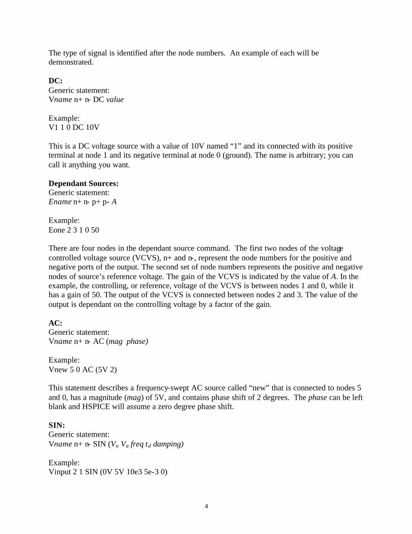
The type of signal is identified after the node numbers. An example of each will be demonstrated. DC: Generic statement: Vname n+ n- DC value Example: V1 1 0 DC 10V This is a DC voltage source with a value of 10V named “1” and its connected with its positive terminal at node 1 and its negative terminal at node 0 (ground). The name is arbitrary; you can call it anything you want. Dependant Sources: Generic statement: Ename n+ n- p+ p- A Example: Eone 2 3 1 0 50 There are four nodes in the dependant source command. The first two nodes of the voltage controlled voltage source (VCVS), n+ and n-, represent the node numbers for the positive and negative ports of the output. The second set of node numbers represents the positive and negative nodes of source’s reference voltage. The gain of the VCVS is indicated by the value of A. In the example, the controlling, or reference, voltage of the VCVS is between nodes 1 and 0, while it has a gain of 50. The output of the VCVS is connected between nodes 2 and 3. The value of the output is dependant on the controlling voltage by a factor of the gain. AC: Generic statement: Vname n+ n- AC (mag phase) Example: Vnew 5 0 AC (5V 2) This statement describes a frequency-swept AC source called “new” that is connected to nodes 5 and 0, has a magnitude (mag) of 5V, and contains phase shift of 2 degrees. The phase can be left blank and HSPICE will assume a zero degree phase shift. SIN: Generic statement: Vname n+ n- SIN (Vo Va freq td damping) Example: Vinput 2 1 SIN (0V 5V 10e3 5e-3 0)
5
Vo is the initial voltage. Va is the voltage amplitude. freq is the frequency. td is the time delay in seconds. damping is the damping factor. This element statement describes a sinusoidal signal named “input” at it is connected between nodes 2 and 1. The signal has an initial voltage of 0V and a magnitude of 5V. It has a frequency of 10kHz and a time delay of 5milliseconds. The signal has no damping factor. If the statement does not contain values for td or damping, then spice assumes a value of zero for both. PULSE: Generic statement: Vname n+ n- PULSE (V1 V2 td tr tf PW T) Example: V50 15 0 PULSE (2 5 0 2e-3 4e-5 5 10) V1 is the lower voltage value. V2 is the upper voltage value. td is the time delay in seconds. tr is the time in seconds it takes for the pulse to rise. tf is the time in seconds it takes for the pulse to fall.
PW is the pulse width of the peak value (or the time the pulse remains at the upper voltage value in seconds). T is the time of one pulse period in seconds. The example details a pulse named “50”. It is connected to nodes 15 and 0. The pulse has a lower voltage value of 2V and an upper value of 5V. The time delay is zero seconds, while it takes 2ms and 40µs for the pulse to rise and fall, respectively. The pulse spends 5 seconds at 5V and has a total period of 10 seconds. PWL: Generic: Vname n+ n- PWL (t1,v1 t2,v2…tn,vn) Eample: V100 25 10 PWL(0,0 3e-3,5V 6e-3,5V 10e-3,-3V) To use a piecewise linear source, state a voltage and the corresponding time you wish the source to reach that value. In the example above at time 0, the source will have a value of 0V. The source will then perform a linear increase for the next 3ms till it reaches 5V. The next point given has the same voltage value, so the source will have the value of 5V for the next 3ms. The source will then follow a linear degradation till it reaches –3V four milliseconds later.
6
Graphs of the time varying signals:
Amplitude (sec)
Vo + Va
e-damp(t-td)
Time (sec)
Vo
(frequency) -1
td
Figure 1.2. A SIN wave created in HSPICE.
Amplitude (volts)
time (sec)T
PW
tftrtd
V2
V1
Figure 1.3. A Pulse wave created in HSPICE.
7
Amplitude (volts)
time(sec)
t6,v6
t5,v5
t4,v4t3,v3
t2,v2
t1,v1
Figure 1.4. A piecewise linear signal created in SPICE.
When dealing with units, there are certain scale-factor abbreviations that HSPICE will recognize. The acceptable abbreviations for HSPICE are listed in table 1.3. Table 1.3 Scaling abbreviations
Spice Abbreviation Metric Prefix Multiplication factor T tera 10
+12
G giga 10+9
Meg mega 10+6
K kilo 10+3
M milli 10-3
U micro 10-6
N nano 10-9
P pico 10-12
F femto 10-15
SPICE does not require you to label the units, however here are the acceptable unit abbreviations.
8
Table 1.4 Unit abbreviations. Spice Abbreviation Units
A Amps Degree Degree
F Farad H Henery Hz Hertz
Ohm Ohms (Ω) V Volts
Caution: If not caught, SPICE has a really fatal flaw. If you notice, the abbreviation for Farads and femto are both “ F ”. This can be a cause for real heart burn. If you were to label your capacitance value 1F thinking this represents one farad, you would soon find out that spice interprets this as 1 femto farad (1e-15 Farads). To be safe, just leave the units off when dealing with capacitance. Passive elements: Passive elements statements are very similar to DC sources. The first letter indicates the passive element that is being used. The letters for a standard resistor, capacitor and inductor are listed in table 1.1. A schematic diagram of each is shown below. The schematic diagrams accompanied by a generic statement, an example statement and a brief explanation.
Figure 1.5. Schematic symbols of a resistor, capacitor, and inductor. Resistor: Generic: Rname n+ n- value Example: R1 5 0 10k The example depicts a resistor named “1”, which is connected between nodes 5 and 0 (ground). It has a value of 10k Ohms. Capacitor: Generic: Cname n+ n- value [IC=initial condition]
9
Example: Cload 50 0 10u [IC=0.5V] This example is a capacitor named “load” connected at nodes 50 and 0 (ground) and it is 10 microfarads. This capacitor also has a 0.5V initial condition. This means that the capacitor has an initial voltage at time equal to zero. If the “[IC=initial condition]” part is left off, SPICE will assume that the initial voltage on the capacitor is zero volts. Caution: Remember the unit problems with capacitors stated earlier. Inductor: Generic: Lname n+ n- value [IC=initial condition] Example: Lfeedback 50 0 1 The inductor is modeled similar to the capacitor, except the initial condition is in terms of current as opposed to voltage. This particular inductor has a 0A initial condition. Active elements: The three basic active elements needed for this class are the diode, BJT and the MOSFET. The element statements for active devices are really similar to passive. The fundamental difference is that the BJT and MOSFET are three and four terminal devices, respectively. The physical characteristics can also be a little more complicated. Other than that, active elements follow the same basic element statement format. The first letter identifies the device type, the next three statements are for the node numbers (only two in the case of the diode), and the last part of the statement contains the physical characteristics. Since active devices have complicated physical characteristics a “.Model” Statement is used. An example of a diode, BJT and MOSFET are all show below. To better illustrate this technique, they will have an accompanying explanation. Diode:
Figure 1.6. A schematic symbol of a diode.
a represents the anode terminal. c represents the cathode terminal.
Generic: *(under device section) Dname a c model_name *(Under Model Statement section) .Model model_name D [certain parameter#1=value certain parameter#2=value … etc ]
10
Example: *(under device section) Drec 2 3 fermi *(under Model Statement section) .Model fermi D [Is=150pA n=1.2] This example is of a diode named “rec”. It is connected between nodes number 2 and 3. This diode references its physical characteristics from a .Model statement called “fermi”. In this particular example the only parameters dictated to Spice are Is and n. More parameters can be specified if desired. Table 1.5 is a list of typical parameters specified for a diode and the default setting for each. Table 1.5 Diode model parameters. Spice Abbreviation Diode Characteristics Units Default
Is Saturation current Amps 1 × 10-14
Rs Ohmic Resistance Ohms 0 n Ideality factor Unit less 1 BV Reverse-bias breakdown voltage Volts 8 IBV Reverse-bias breakdown current Amps 1× 10⁻¹⁰ BJT:
Figure 1.7. Schematic symbol for BJTs.
B is the Base terminal C is the Collector terminal
E is the emitter terminal. The BJT element statement is very similar to the diode. The main difference is that it has three terminals instead of two. Other than that, the structure of the statement is very similar. An example of a NPN is done below. Generic: *(under device section) Qname C B E model_name *(under Model Statement section) .Model model_name NPN [certain parameter#1=value, certain parameter#2=value,…,etc ]
11
Example: *(under device section) Q1 3 14 5 normal *(under Model Statement section) .Model normal NPN [Is=3e-14, Bf=150, Vaf=30V ] The example statement describes a BJT with its collector connected at node 3, base connected at node 14, and emitter connected at node 5. It references the “.model” statement called “normal” for all the physical characteristics. “normal” indicates to Spice that the BJT called “1” is an NPN transistor and gives some associated characteristics. The “.Model” statement is easily modified to change the transistor to a PNP type. Simply replace the NPN with PNP in the statement. Table 1.6 give some basic characteristics variables for a typical BJT and the default values associated with each. Table 1.6 BJT model parameters. Spice Abbreviation Model Parameter Units Default
Is Saturation current Amps 1 × 10-16
Bf Forward Gain Unit less 100 Rb Base resistance Ohms (Ω) 0 Rc Collector resistance Ohms (Ω) 0 Re Emitter resistance Ohms (Ω) 0 VAf Forward Early voltage Volts 8 MOSFET:
Figure 1.8. Schematic symbol of MOSFETS
G is the Gate terminal D is the Drain terminal S is the Source terminal B is the Bulk terminal
12
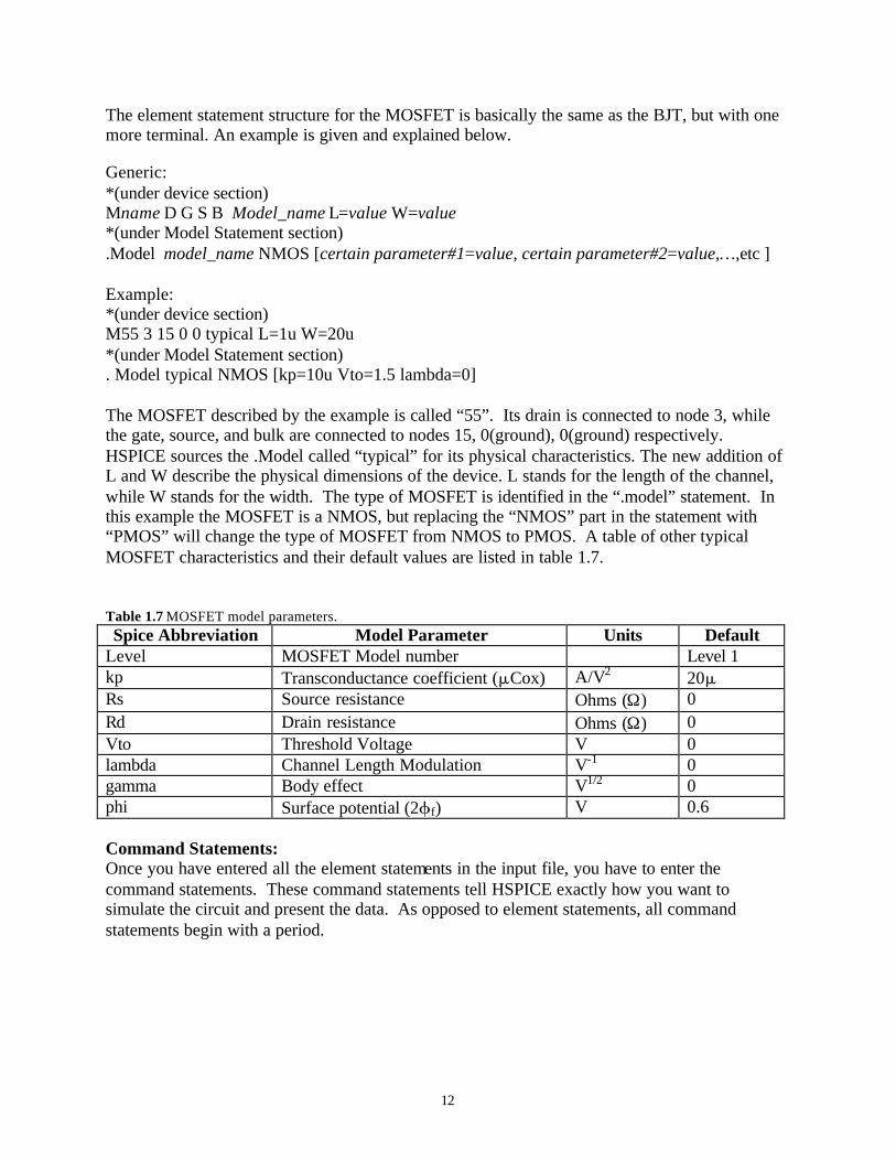
The element statement structure for the MOSFET is basically the same as the BJT, but with one more terminal. An example is given and explained below. Generic: *(under device section) Mname D G S B Model_name L=value W=value *(under Model Statement section) .Model model_name NMOS [certain parameter#1=value, certain parameter#2=value,…,etc ] Example: *(under device section) M55 3 15 0 0 typical L=1u W=20u *(under Model Statement section) . Model typical NMOS [kp=10u Vto=1.5 lambda=0] The MOSFET described by the example is called “55”. Its drain is connected to node 3, while the gate, source, and bulk are connected to nodes 15, 0(ground), 0(ground) respectively. HSPICE sources the .Model called “typical” for its physical characteristics. The new addition of L and W describe the physical dimensions of the device. L stands for the length of the channel, while W stands for the width. The type of MOSFET is identified in the “.model” statement. In this example the MOSFET is a NMOS, but replacing the “NMOS” part in the statement with “PMOS” will change the type of MOSFET from NMOS to PMOS. A table of other typical MOSFET characteristics and their default values are listed in table 1.7. Table 1.7 MOSFET model parameters. Spice Abbreviation Model Parameter Units Default
Level MOSFET Model number Level 1 kp Transconductance coefficient (µCox) A/V2 20µ Rs Source resistance Ohms (Ω) 0 Rd Drain resistance Ohms (Ω) 0 Vto Threshold Voltage V 0 lambda Channel Length Modulation V-1 0 gamma Body effect V1/2 0 phi Surface potential (2φf) V 0.6 Command Statements: Once you have entered all the element statements in the input file, you have to enter the command statements. These command statements tell HSPICE exactly how you want to simulate the circuit and present the data. As opposed to element statements, all command statements begin with a period.
13
Analysis type: Once the element statements are complete, the analysis that is to be done needs to be specified to HSPICE. This is done with an analysis request statement. When creating an input file, you must decide from the start what type of analysis you want to perform. As listed in table 1.2, some independent sources only work with certain types of analysis. There are four basic types of analysis to choose from: DC operating point, DC sweep, AC frequency response, and transient response. An example of each analysis request statement is done below. DC operating point requested: .OP DC sweep: Generic statement .DC source_name starting_value ending_value step_value Example: .DC power 0V 5V 0.1V A DC sweep is done for many reasons. For example, you would use a DC sweep if you wanted to see the different responses of a circuit for different biasing conditions. In the example the “.DC” analysis command instructs the source named “power” in the circuit to start at 0V and increase its values by increments of 0.1V until it reaches a value of 5V, then it stops. You would then use a specific output request to see the response (this will be discussed later). AC frequency response: Generic: .AC type number_of_points frequency_start frequency_stop There are three different types of AC frequency responses. The difference deals with how the points are taken. You can specify the following types: DEC (points are spaced logarithmically by decade), OCT (points are spaced logarithmically by octave), or LIN (points are linear spaced). Example of the three different types: .AC DEC 100 2k 1e6 .AC OCT 1000 2k 1e6 .AC LIN 50 500 550 The “.AC” command does not need the name of the source. An AC source is the only source that allows for this type of analysis, so HSPICE will implement this analysis to the AC source in the circuit automatically. The first “.AC” command depicts a statement that performs a frequency sweep that takes 100 points per decade. The analysis starts at 2kHz and ends at 1MHz. The other two statements follow the same format. Following the “.AC” command are
14
statements that indicates the way points are taken and the number of points taken, respectively. Finally, the starting and ending frequencies are listed. Transient response: Generic: .TRAN step_time stop_time Example: .TRAN 10n 10m This example simulates the circuit for 10ms and takes data points every 10ns. The “.TRAN” analysis is preformed when the response of the circuit with time is desired. For example, a transient response request would be used if you wanted to see the time it takes a capacitor to charge or discharge. Caution: For correct data collection, make sure that the smallest step time in the transient command is equal to or smaller then the fastest change in your signal. You must also make sure that the transient time complements the source, or you will not be able to see the simulated results. Output requested: With HSPICE you can request the data collected to be in the form of data points or as plot. This is done with a “.PRINT” or “.PLOT” statement. The type of print or plot statement depends on what type of analysis you requested. Table 1.8 lists these statements. Table 1.8 Output data type requests.
Output requested Analysis Spice Command Print data points DC .PRINT DC output AC .PRINT AC output TRAN .PRINT TRAN output Plot data points DC .PLOT DC output [(lower_ limit upper_limit)] AC .PLOT AC output [(lower_ limit upper_limit)] TRAN .PLOT TRAN output [(lower_ limit upper_limit)] You will be able to view the data collected in the output file that is created once you simulate the input file through HSPICE. The output gives information on what you are measuring (you can measure voltage, voltage difference, or current through any element) and the node number where you want to observe the activity of the circuit. You many request data from multiple outputs, just separate the “output” requests with a space. Table 1.9 lists different “output” statements that may be used to measure voltage, voltage difference, or current in a circuit.
15
Table 1.9 Data collection methods for .print and .plot commands.
Measuring “output form” Voltage at a specific node V(node_number) Voltage difference between two nodes V (node_number1, node_number2) Current through any element I(Element_name) Some examples are done below. Example: .PLOT DC V(5) V(6) (-15 +15) This plots the voltage at nodes 5 and 6 on a graph with the y axis having a range from –15V to +15 V. Example: .PRINT TRAN I(R1) V(15) This statement will print all the data points collected for the current going through the resistor called “1” and voltage at node “15”. Special “output” requests: Some special “output” requests can be made for AC simulations . Just switch the identifying letter (V or I) in the “output form” listed above with a new abbreviation listed in table 1.10. Table 1.10 Output requests.
Measuring New Abbreviation Real part Vr, Ir Imaginary part Vi, Ii Magnitude Vm, Im Phase Vp, Ip Decibels Vdb, Idb After you have entered all the elements, analysis, and output request you must end the input file with an “.END” statement. Make sure to press return after you have typed your .END statement. Not doing this sometimes hang ups HSPICE. Graphical Interface Plots: HSPICE plots are very crude and not the most presentable. There are tools that you can use to plot the data once you have collected it. You can use the “.PRINT” statement, then copy and paste the output data into excel or an equivalent and plot it that way. There are also graphical interface programs designed to plot the data stored in you output file automatically. One such program is “mwaves”. If you want to use mwaves you must include the statement “.opt post”
16
right before your element statements. If you are using mwaves and you just want to plot outputs, then you don’t need to include any “.PLOT” or “.PRINT” statements. Type the following command to simulate. unix prompt:HSPICE file_name.sp Unlike before, you will not be able to look at the traditional output file with this command. If you wish to look at the complete Spice output file, then use the simulation command given earlier. Once the simulation is complete, HSPICE should create a file with the same name as the input file. The difference will be the extension will be“.st0” or “.tr0” (ex. filename.st0, or filename.tr0). Depending on which type is created use the following command at the UNIX prompt to use mwaves. Unix prompt:mwaves filename.st0 or Unix prompt:mwaves filename.tr0 Two windows should pop up. One that is titled “AWAVES” and the other is titled “Result Browser”. On the “Result Browser” you should be able to just point and click on the type of analysis you want, then you double click on the node number you want plotted. Play around with mwaves, there are many options that you may use with it. Example of an input file: Example input file * * .opt post Vs 2 0 SIN ( 0V 1V 10k) R1 2 1 10k D1 1 0 diode * * .MODEL diode D (Is=2E-13 N=1.1) .OP .TRAN .01m 1m .PLOT TRAN V(1) .END Note: HSPICE is case insensitive.
17
A Schematic of the example input file.
Figure 1.9. Schematic of example input file. The output waveform produced by mwaves:
Figure 1.10. Signals plotted using mwaves.
This lab is no way intended to be an HSPICE manual. This introduction only covers the basics that a student will need to run HSPICE. Other published material, such as the ones in the reference reading, on SPICE should be consulted for a better understanding.
18
Reference Reading
1. Gordon W. Roberts and Adel S. Sedra. SPICE. Second edition. New York: Oxford Press, 1997. 2. Marc E. Herniter. Schematic Capture with MicroSim Pspice. Third edition. Upper Saddle River, New Jersey: Prentice Hall, 1998. 3. R. Mararem. EE 202 notes. University of Southern California, Fall 2000.
19
Lab exercise Part 1.
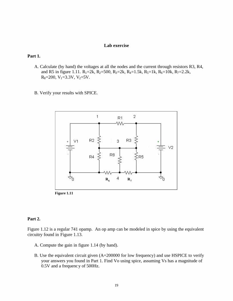
A. Calculate (by hand) the voltages at all the nodes and the current through resistors R3, R4, and R5 in figure 1.11. R1=2k, R2=500, R3=2k, R4=1.5k, R5=1k, R6=10k, R7=2.2k, R8=200, V1=3.3V, V2=5V.
B. Verify your results with SPICE.
R6 R7
Figure 1.11
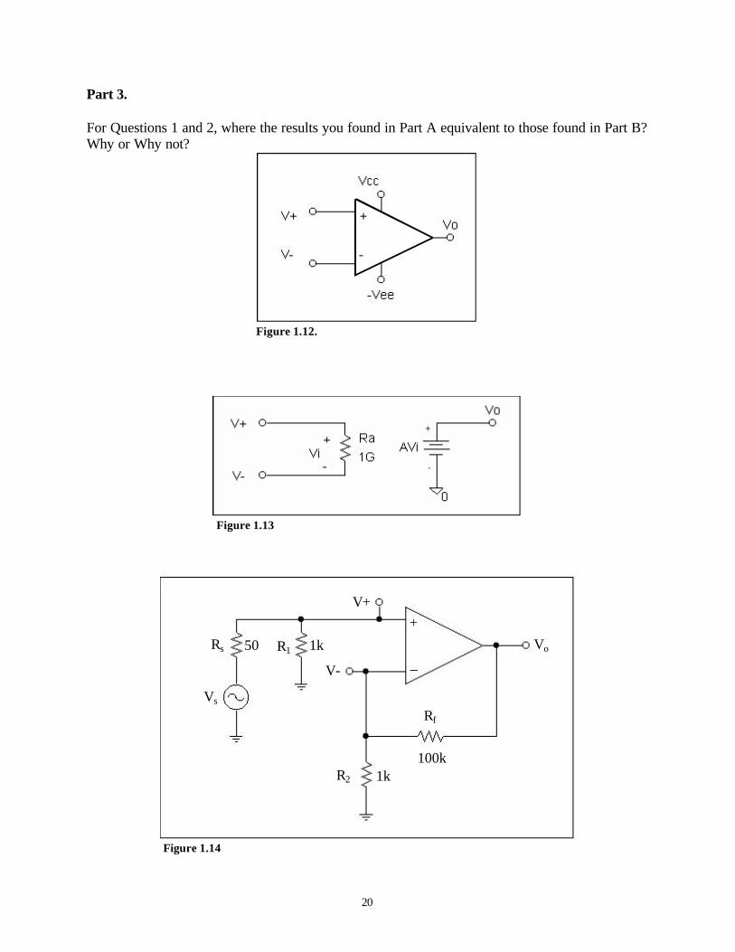
Part 2. Figure 1.12 is a regular 741 opamp. An op amp can be modeled in spice by using the equivalent circuitry found in Figure 1.13.
A. Compute the gain in figure 1.14 (by hand).
B. Use the equivalent circuit given (A=200000 for low frequency) and use HSPICE to verify your answers you found in Part 1. Find Vo using spice, assuming Vs has a magnitude of 0.5V and a frequency of 500Hz.
20
Part 3. For Questions 1 and 2, where the results you found in Part A equivalent to those found in Part B? Why or Why not?
Figure 1.12.
Figure 1.13
Vs
Rs R1
+
_
V+
V-
Vo
Rf
100k R2 1k
50 1k
Figure 1.14
21
Part 4.
A. Using a transient simulation on the circuit in figure 1.15 to plot Vo vs Vs. Vs is a pulse generating source that alters between 0V and 5V. The source should have a 1ms delay, 5ms pulse width, 10ms period, and a rise and fall time of 1ps. Using a capacitor equal to 0.1µF and a resistor of 2kΩ plot Vo vs Vs for the following transient simulation times;
i) 30ms ii) 300ms iii) 0.3ms
B. Do the results differ when using three different simulation times? Why is it important to
make an educated decision when choosing a simulation time for your simulation?
Figure 1.15
Part 5.
A. Using the schematic in figure 1.15, perform an .AC analysis. Replace Vs with an AC source with a magnitude of 1V. Change R1 and C1 to 1kΩ and .1nF, respectively. Perform an AC sweep in the following frequency ranges;
i) 10-1kHz ii) 10-10kHz
B. One can see that choosing the correct frequency range optimizes the results. What would be the problem with being safe and simulating all circuits to 10GHz?