Extraction of intrinsic structure for Hardware Trojan detection Maxime Lecomte [email protected]Jacques J.A. Fournier [email protected]Philippe Maurine [email protected]September 18, 2015 Abstract In this paper we present a novel solution to address the problem of potential malicious circuitry on FPGA. This method is based on an a technique of structure extraction which consider the infection of an all lot. This structure is related to the design (place and route, power grid. . . ) of the integrated circuits which composes the lot. In case of additional circuitry this design will be modify and the extracted structure will be affected. After developing the extraction techniques we present a method- ology to insert detection of hardware trojan and counterfeit in different IC manufacturing steps. At last an application example using 30 FPGA boards validate our extraction method. Finally, statistical tools are then applied on the experimental results to distinguish a genuine lot from an infected one and confirm the potential of detection the extracted struc- ture. 1 Introduction Due to the recent trend of outsourcing integrated circuit (IC) manufacturing and design, structural integrity verification of ICs has become a hot topic. From the specification step to that of packaging, and especially during the design step, a circuit can be corrupted by a malicious adversary. This malicious alteration of the IC structure is called a Hardware Trojan (HT) insertion and its effects can range from performance degradation (e.g. denial of service) up to more sophisticated functionalities (memory dumping etc) [21]. Similarly with the multiplication of foundries and IC vendors, counterfeits are spreading rapidly, ranging from simple copies to a complete replacement of an given IC by one of lower quality. A HT is composed of two parts: the trigger and the payload. The trigger is the mechanism that scans some signals within the IC until a specific condition 1
In this paper we present a novel solution to address the problem ofpotential malicious circuitry on FPGA. This method is based on an atechnique of structure extraction which consider the infection of an all lot.This structure is related to the design (place and route, power grid. . . )of the integrated circuits which composes the lot. In case of additionalcircuitry this design will be modify and the extracted structure will beaffected. After developing the extraction techniques we present a method-ology to insert detection of hardware trojan and counterfeit in differentIC manufacturing steps. At last an application example using 30 FPGAboards validate our extraction method. Finally, statistical tools are thenapplied on the experimental results to distinguish a genuine lot from aninfected one and confirm the potential of detection the extracted struc-ture.
1 Introduction
Due to the recent trend of outsourcing integrated circuit (IC) manufacturing anddesign, structural integrity verification of ICs has become a hot topic. From thespecification step to that of packaging, and especially during the design step,a circuit can be corrupted by a malicious adversary. This malicious alterationof the IC structure is called a Hardware Trojan (HT) insertion and its effectscan range from performance degradation (e.g. denial of service) up to moresophisticated functionalities (memory dumping etc) [21]. Similarly with themultiplication of foundries and IC vendors, counterfeits are spreading rapidly,ranging from simple copies to a complete replacement of an given IC by one oflower quality.
A HT is composed of two parts: the trigger and the payload. The trigger isthe mechanism that scans some signals within the IC until a specific condition
1
is met. When this condition is met, the payload is activated. The triggercan either be generated externally (external signals or physicals condition) orinternally (a special internal state, data, etc). Moreover the trigger can either becombinational (result of a logical operation) or sequential (related to a successionof states). The payload is the ‘malicious’ effect of the HT. It can either beexplicit where of signals are directly added, removed or deactivated. It canalso be implicit where the effect cannot be directly observed like, for example,adding side-channel information in the power consumption. The detection ofa HT before its activation is a difficult task and it still remains a challengingproblem even after its activation when the payload is implicit.
The probability of triggering a HT during functional tests is low and testingis an expensive approach to that end. Moreover, inspecting the circuit throughreverse engineering is an expensive process in terms of cost and time and canbe destructive. This solution can therefore be applied to only few devices, eventhough latest imaging based methods have proven to offer a simpler and fasteralternatives [9].
Several non destructive methods for HT detection have been recently pro-posed. The first proposed approaches analyze, using statistical techniques, theoverall consumption of an IC to detect the impact of the HT. For example,in [2], a detection technique based on the Karhunen-Loeve theorem is proposedin order to detect the power consumption of the HT within process variationsand noise. However, this paper only reports validations obtained by simulations,omitting things like the measurement noise. Moreover, the technique may notscale to complex Systems on Chip (SoC).
Hence, in order to enhance the detection capabilities, techniques have beenproposed in [14] to analyze locally the propagation delays of logical paths withembedded monitors. However, once again, only simulation results are provided.Another method has been proposed in [1] to integrate a hardware system al-lowing to monitor important nets of ICs. However, little information is givenin this paper about the efficiency of the proposed technique. In parallel to thisapproach, a test solution was also proposed in [8] in order to trigger easily a HTor at least to increase their electrical activity.
In [16], a first attempt to suppress process variations from the HT detectionproblem has been proposed based on the strong correlation between the max-imum operating frequency of ICs, Fmax, and their dynamic power consump-tion. This approach however faces the difficult problem of measuring Fmax onSoCs [5, 17].
Then in 2011, the use of Ring Oscillators (RO) has been proposed to detectHTs. For example, in [13] the authors propose an analysis of RO sensitivity tothe presence of HT but conclude that it seems difficult to detect really smallHT. In parallel [24] proposes the use of an array of RO, used in conjunction witha Principal Component Analysis (PCA) [10], to distinguish infected ICs fromgenuine ones. This proposal has been experimentally validated on an FPGAusing a Digital Sampling Oscilloscope (DSO) (thus off-chip) to measure theoscillating frequency of ROs. This idea has then be applied to design an ASICin 2012 [11] where the initial results were only partly validated. This is may
2
due to the use of an embedded 8-bit counter as RO, which reduces the accuracyof the measured frequencies.
Later in 2013, the authors in [6] propose to cluster, during the design step,the power grid in several voltage islands embedding each a dedicated sensor toenhance the detection capability. However, no experimental results are givenin this paper, neither on the improvements obtained nor on the cost in termsof Silicon area. In 2014, [19] describes a method based on the use of near fieldelectromagnetic cartography. Yet, the authors conclude that it seems difficult todetect all the HT. However, in [3], a more efficient technique is used to interpretthe EM traces. As a result, authors conclude it is possible to detect really smallHTs but with a special care to control the temperature during measurements.Finally, in [23] the authors analyze EM emanations from FPGAs and succeedsto differentiate a genuine population from an infected one.
Based on those results, the on-chip monitoring solutions seem relevant interm of efficiency since the obtained detections rates are higher than for off-chipmethods. Furthermore, these solutions seem industrially viable since the costof the equipments, dedicated to the data acquisition, is reduced as the tests caneasily be done in parallel. For those reasons, the work presented here is basedon on-chip methods.
In this paper, we consider that the infection of a single device is not realisticbased on the current life cycle of ICs (mainly linked to production and distri-bution constraints). That why the HT detection methodology proposed in thispaper does not aim at establishing if an IC is infected but aims at checkingthe integrity of a whole production lot. Moreover, this approach also allows todetermine if a given IC is a counterfeit (apart from the case of a really highquality copy). The principle of the proposed methodology is to detect, thanksto a embedded sensor network, an alteration in the design’s structure inducedby the presence of a HT, or by a modification in its place and route or in itsfloor-plan. These alterations modify the IC power distribution and in particularthe static voltage drops [15] in the glue logic and hence that in the sensor array.This method is based on a novel variation model of the performance of CMOSstructures in real designs (not in test chips dedicated to the fine measurementof the intra and inter die variations), model which is introduced and validatedin this paper.
The paper is organized as follows. First, section 2 describes the threats toIC integrity and specifies which ones are covered in this paper. Then section3 introduces the proposed variation model and defines the basic principle ofour detection methods. Section 4 details the HT and counterfeited detectionmethodology and section 5 describes the experimental results which validatethe proposed approach and the proposed variation model on a set of 30 FPGAs.Finally, the wide range of perspectives generated by our approach is discussed,as a conclusion, in section 6.
3
Design center
Manufacturing Usage
Trojan Insertion
IP vendors Trojan Insertion
Trojan Insertion
(1)
(2)
(3)
(4)
Figure 1: Mains threats to IC integrity
2 Threats and characteristics of infected devicesand counterfeits
First, this section recalls briefly the main threats to IC integrity. Second, theHT and counterfeit detection method is described specifying which threats itcovers.
2.1 Threats to IC integrity
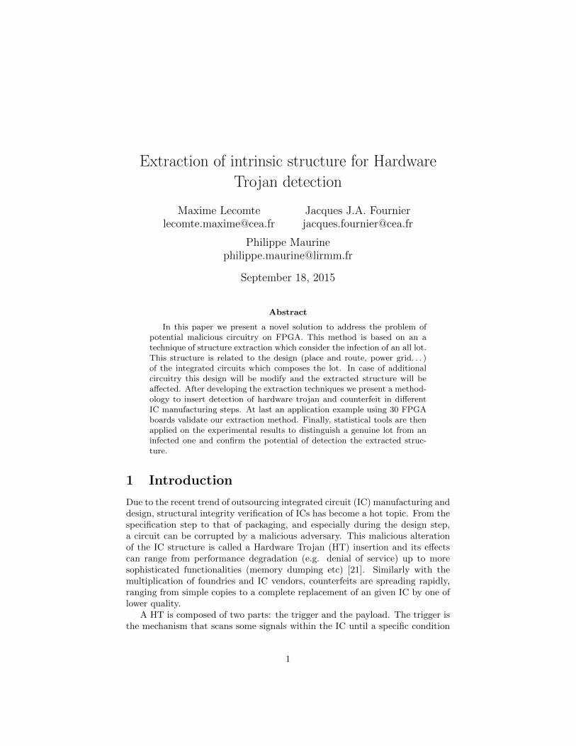
Fig. 1 summarizes the different steps, from design to exploitation, for manu-facturing an IC and the associated threats. The first vulnerabilities are at thedesign stage. A corrupted piece of hardware IP can be introduced into the prod-uct (Threat (1) in Fig. 1) or a compromised employee from the design center canintroduce a HT into the HDL description (Threat (2) in Fig. 1). It is difficultto protect against such threats, but some solutions based on ad-hoc design andverification methods have been proposed [7, 18,22].
The second vulnerable stage is the manufacturing (Threat (3) in Fig. 1).For example, filler cells can be substituted by logic gates, inducing a denial ofservice or more complex functionalities, or a fuse can be disabled etc. A lastthreat is that of counterfeits. It consists in selling second hand products, lowerquality devices or functional copies directly onto the market causing financial
4
losses (Threat (4) in Fig. 1). Some can even be almost perfect copies which aredifficult to detect.
2.2 Features of infected circuits or counterfeits
Many methods have been proposed to detect HTs. Among them, a large major-ity aims at detecting the parasitic electrical activity (additional power consump-tion) generated by the HT’s trigger. However, this parasitic electrical activity isnot the only measurable trace left by the HTs. Another one is the alteration ofthe inner structure of the IC. For example, the HT insertion modifies the localand global capacitance and resistance of the power and ground nets. This mod-ification induces a different current flow in the IC, and thus a different static ordynamic voltage distribution (static or dynamic voltages drops).
In the same way, counterfeits are characterized by a more (functional copies)or less (almost exact hardware copy) different physical structures, and thereforeby a different repartition of the voltage across the IC’s surface.
3 Principle of HT and counterfeit detection
Our detection method is based upon a simple principle: a fingerprinting of thesupply voltage on the surface of IC at rest (i.e. just powered on with the clockactive). In order to do this, a network of sensors is uniformly spread over thewhole IC surface to get a cartography of the inner supply voltage. Any sensorsensitive to the supply voltage, V dd, can be used. In the experiments reportedin section 5, Ring Oscillators (RO) are used. Given that the frequency f of aRO is sensitive to the local V dd value, the distribution of measured values forf above the IC surface, in the absence of any process variation (P), is a directpicture of the V dd distribution. Hence in our approach, we have to get rid of theeffect of intra-die and inter-die process variations. With this approach, we shallbe able to mitigate risks linked the introduction of HTs at the manufacturingstage.
3.1 Process variation model and performance variationmodel of CMOS structures
Given p, an inherent parameter of the IC fabrication technology, the impactof the manufacturing process variations, the so called process variations, aregenerally described as follows:
p = p+ ∆pinter + ∆pintra (1)
with p being the mean (or typical) value of the parameter on a whole lot of aproduction, ∆pinter ∼ N(0, σ2
inter) the effect of the inter-die variations assumednormal and ∆pintra ∼ N(0, σ2
intra) the impact of variations within a die, i.e. theintra-die process variations also assumed normal.
5
This process variation model is well known and widely adopted to simulatethe effect of process variations on the parameter p of an IC (a transistor, a re-sistance, a pn junction, etc). However, the extraction of the standard deviationvalues σintra and σintra is generally performed on dedicated ICs (regular arraysof MOS transistors [12] or SRAM cells [4]) which are quite uniform relative totheir physical structures and under controlled voltage and temperature. Thisprocess variation model does not take into account the impact of the IC’s phys-ical structure (power supply routing, local transistor density, etc) on the CMOSgate performance or on that of an embedded sensor which, of course, dependson all process variations through equation (1). Hence for our case, we shall usethe following variation model for the output value T (xi, yi) of a sensor i locatedat (xi, yi) on the IC’s surface:
T (xi, yi) = T + ∆Tinter + ∆Tintra + ∆T (xi, yi) (2)
where ∆T (x, y) is a deterministic value which depends of the sensor’s positionover the IC, and which models the impact of the IC’s structure on the per-formance of the sensor. To ease the reading, T (xi, yi) and ∆T (xi, yi) shall benoted Ti and ∆Ti respectively, showing that the variation model considered inthis paper is a spatial model.
3.2 Fingerprinting the IC’s structure
Considering the model given by equation (2), fingerprinting the structure of adesign featuring a network of q sensors regularly spread on its surface is relativelysimple for a same manufacturing lot of ICs. The q values of ∆Ti are calculatedby averaging the impact of the process variations on mlot devices of the samelot:
∆Ti =1
mlot·mlot∑j=1
T ji − T =
1
mlot·mlot∑j=1
∆T ji (3)
σ∆Ti=
√√√√ 1
mlot·mlot∑j=1
(∆T ji − ∆Ti)2 (4)
where:
T =1
mlot · q·mlot∑j=1
q∑i=1
T ji (5)
T ji is the measurement of the output of the sensor i of the device j ∈ {1, . . . ,mlot}
of the considered lot.With these notations, the vector SDesign = [sDesign
1 , . . . , sDesign2q ] can be de-
fined as follows:
SDesign = [∆T1, . . . , ∆Tq, σ∆T1, . . . , σ∆Tq
] (6)
6
SDesign represents the fingerprint of the physical structure of an IC called ‘De-sign’ and is by construction independent of the process variations. This fin-gerprint is the base of the HT and counterfeit detection methods proposed insection 4.
4 Detection Methodology
The starting point of our methodology is the addition of a network of sensorssensitive to the supply voltage. Those sensors are placed so as to cover most ofthe IC’s surface. The granularity, i.e. the distance between two sensors, is chosenby the IC designer depending on the trade-off between detection capability andcost.
When the first run or the test run (which are less likely to be infected) isreceived, the integrity of some devices is verified to qualify the whole lot. Thiscould be done by applying reverse engineering methods or by using optical basedmethods [20]. Once the first production lot is qualified, the signature (see eq.(6)) of the design is calculated using equations (3) and (4). This fingerprintconstitutes the reference fingerprint for the considered design.
The designer will then usually order other runs (“production runs”) fromthe same foundry or from another one which offers the same technology node.Once those new production lots are received, their corresponding fingerprintsare calculated and are ‘compared’ with the reference one in order to verify thatthe newly received lots have not been corrupted. Ageing techniques could beapplied to this reference lot to derive fingerprints of the design at different ages.
In the same way, at some (later) point in time, the designer can have ‘fieldreturns’ which could contain counterfeits. With the reference fingerprint, theorigin of these devices can be verified without application of expensive, complexand destructive methods. In order to do that, the designer extracts the finger-print of the suspected device and compares it with the reference fingerprint tofinally get a probability that the device is a genuine one. If the probability istoo low, complementary analyses (like reverse engineering) can be applied.
The above procedures require the comparison of the reference fingerprintwith that of a new production lot in order to detect the eventual presence of anHT (case 1). The procedures also require the comparison of the reference finger-print SREF with the fingerprint of a single device in order to detect counterfeits(case 2).
4.1 Case 1:HT detection
When the integrity of a new lot of devices has to be checked, the first step isto calculate its fingerprint SNewRun. Since this signature shall be, in practice,calculated using a high number of devices (> 100), the estimate of means canbe considered as reliable. It is therefore possible to apply distinguishers or astatistical tools working on the means, like the Difference of Means (DoM) or
the T-test (and more precisely the Welch’s test). This implies using the ∆Tis
7
of the signatures (eq. (6)) and to analyze the values
∆Si = SRefi − SNewRun
i (7)
for i = {1, . . . , q}, or that of
T Stati =SRefi − SNewRun
i√(sRef
q+i )2
mlot− (sNewRun
q+i )2
mlot
. (8)
It is also possible to use other statical tools such as the Kolmogrow-Smirnovtest (KS) to determine if the distributions for all j ∈ {1, . . . ,mlot} of (Tj
i − T)for the reference lot and for the new one are drawn from the same distributionlaw, i.e. if the devices embed the same design or not.
With the same idea of comparing centered populations of (Tji − T), clustering
solutions can be used such as the k-means (with k = 2) or using simply the
median. To do this, the populations (Tji − T) of the reference lot and of the
new lot are merged within the same set. Then, the k-means is applied on theresulting population (or the median is calculated) so that to split it into twoclusters. Finally, the number of devices in each cluster coming from the referencelot and from the new one are counted. If the tested ICs are genuine, the tworesulting clusters have the same number of elements from the reference lot andthat of the new lot. More precisely, if the cardinals of the reference lot and thatof the new lot are equal, 50% of the devices from the reference lot and 50% ofthe devices from the new lot have to constitute each cluster. If this is not thecase, the new lot can be considered as different from the reference one.
4.2 Case 2: counterfeit detection
The case of the suspected ‘field return’ is more difficult to treat as the fingerprintas described so far for HT detection cannot be calculated on one single device:we only have the TSuspected
i of the considered device. In this case, we first“recenter” all the values using the value TSuspected of the suspected IC (i.e.
calculate TSuspectedi − TSuspected) and then calculate the probabilities that each
TSuspectedi values comes from the normal distribution:
N(0, (sSuspectedq+i )2) = N(0, σ2
∆Ti) (9)
σ∆Ti
is indeed the standard deviation of the sensor i, value estimated with theICs from the reference lot. The probabilities for all sensors are then combined(and more precisely a multi-normal distribution is defined with all σ
∆Ti) to
obtain the probability that the considered device is a genuine one.
5 Experimental results
The HT detection methodology has been experimentally tested on a set of 30FPGA boards featuring a Xilinx Spartan3E-1600. 15 boards have been used
8
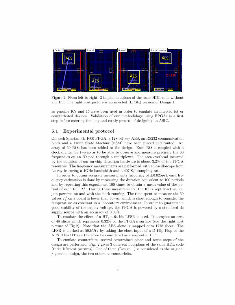
Design 1 Design 2 Design 3 Design 1 infected
LFSR
AES
AES AES
AES
FSM FSM FSM RS232 RS232 RS232 RS232 FSM
Figure 2: From left to right: 3 implementations of the same HDL-code withoutany HT. The rightmost picture is an infected (LFSR) version of Design 1.
as genuine ICs and 15 have been used in order to emulate an infected lot orcounterfeited devices. Validation of our methodology using FPGAs is a firststep before entering the long and costly process of designing an ASIC.
5.1 Experimental protocol
On each Spartan-3E-1600 FPGA, a 128-bit-key AES, an RS232 communicationblock and a Finite State Machine (FSM) have been placed and routed. Anarray of 60 ROs has been added to the design. Each RO is coupled with aclock divider by two so as to be able to observe and measure precisely the 60frequencies on an IO pad through a multiplexer. The area overhead incurredby the addition of our on-chip detection hardware is about 3.2% of the FPGAresources. The frequency measurements are performed with an oscilloscope fromLecroy featuring a 4GHz bandwidth and a 40GS/s sampling rate.
In order to obtain accurate measurements (accuracy of ±0.025ps), each fre-quency estimation is done by measuring the duration equivalent to 100 periodsand by repeating this experiment 100 times to obtain a mean value of the pe-riod of each RO: T j
i . During these measurements, the IC is kept inactive, i.e.just powered on and with the clock running. The time spent to measure the 60values T j
i on a board is lower than 30min which is short enough to consider thetemperature as constant in a laboratory environment. In order to guarantee agood stability of the supply voltage, the FPGA is powered by a stabilized dcsupply source with an accuracy of 0.05%.
To emulate the effect of a HT, a 64-bit LFSR is used. It occupies an areaof 48 slices which represents 0.32% of the FPGA’s surface (see the rightmostpicture of Fig.2). Note that the AES alone is mapped onto 1778 slices. TheLFSR is clocked at 50MHz by taking the clock input of a D Flip-Flop of theAES. This HT can therefore be considered as a sequential HT.
To emulate counterfeits, several constrained place and route steps of thedesign are performed. Fig. 2 gives 3 different floorplans of the same HDL code(three leftmost pictures). One of them (Design 1) is considered as the original/ genuine design, the two others as counterfeits.
9
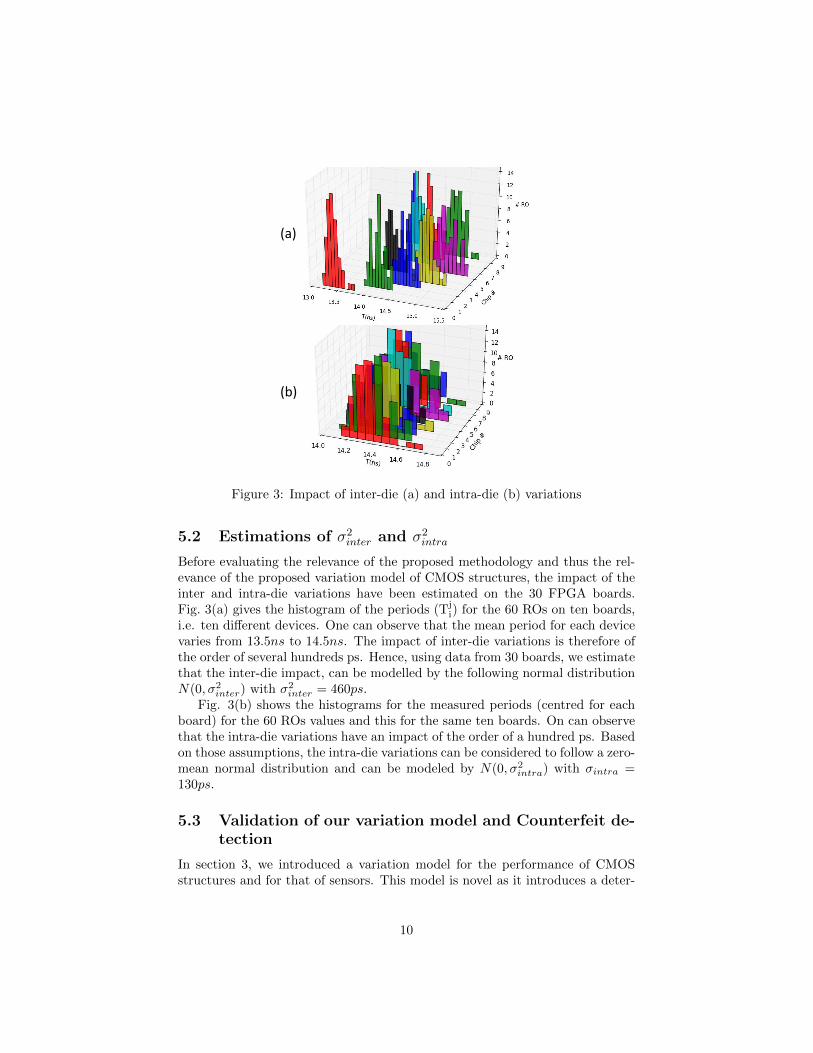
(a)
(b)
Figure 3: Impact of inter-die (a) and intra-die (b) variations
5.2 Estimations of σ2inter and σ2
intra
Before evaluating the relevance of the proposed methodology and thus the rel-evance of the proposed variation model of CMOS structures, the impact of theinter and intra-die variations have been estimated on the 30 FPGA boards.Fig. 3(a) gives the histogram of the periods (Tj
i) for the 60 ROs on ten boards,i.e. ten different devices. One can observe that the mean period for each devicevaries from 13.5ns to 14.5ns. The impact of inter-die variations is therefore ofthe order of several hundreds ps. Hence, using data from 30 boards, we estimatethat the inter-die impact, can be modelled by the following normal distributionN(0, σ2
inter) with σ2inter = 460ps.
Fig. 3(b) shows the histograms for the measured periods (centred for eachboard) for the 60 ROs values and this for the same ten boards. On can observethat the intra-die variations have an impact of the order of a hundred ps. Basedon those assumptions, the intra-die variations can be considered to follow a zero-mean normal distribution and can be modeled by N(0, σ2
intra) with σintra =130ps.
5.3 Validation of our variation model and Counterfeit de-tection
In section 3, we introduced a variation model for the performance of CMOSstructures and for that of sensors. This model is novel as it introduces a deter-
10
𝑺𝑫𝒆𝒔𝒊
𝒈𝒏 𝟏
(𝒑𝒔)
𝑇𝑖𝑗 − 𝑇 (i=24)
𝑺𝑫𝒆𝒔𝒊𝒈
𝒏 𝟏(𝒑
𝒔)
(a)
(b)
400
0
-400
0
-200
400
600
200
200
-200
10 20 30 40 50 60 RO #
0
10 20 30 40 50 60 RO #
0
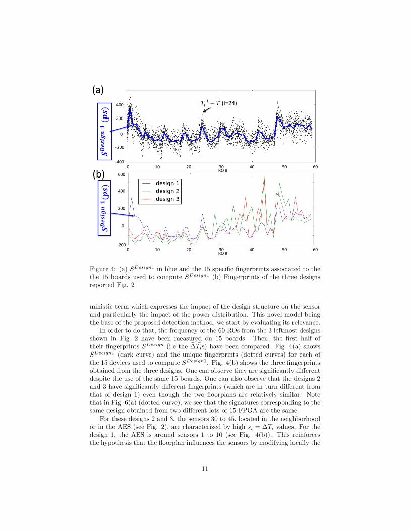
Figure 4: (a) SDesign1 in blue and the 15 specific fingerprints associated to thethe 15 boards used to compute SDesign1 (b) Fingerprints of the three designsreported Fig. 2
ministic term which expresses the impact of the design structure on the sensorand particularly the impact of the power distribution. This novel model beingthe base of the proposed detection method, we start by evaluating its relevance.
In order to do that, the frequency of the 60 ROs from the 3 leftmost designsshown in Fig. 2 have been measured on 15 boards. Then, the first half oftheir fingerprints SDesign (i.e the ∆Tis) have been compared. Fig. 4(a) showsSDesign1 (dark curve) and the unique fingerprints (dotted curves) for each ofthe 15 devices used to compute SDesign1. Fig. 4(b) shows the three fingerprintsobtained from the three designs. One can observe they are significantly differentdespite the use of the same 15 boards. One can also observe that the designs 2and 3 have significantly different fingerprints (which are in turn different fromthat of design 1) even though the two floorplans are relatively similar. Notethat in Fig. 6(a) (dotted curve), we see that the signatures corresponding to thesame design obtained from two different lots of 15 FPGA are the same.
For these designs 2 and 3, the sensors 30 to 45, located in the neighborhoodor in the AES (see Fig. 2), are characterized by high si = ∆Ti values. For thedesign 1, the AES is around sensors 1 to 10 (see Fig. 4(b)). This reinforcesthe hypothesis that the floorplan influences the sensors by modifying locally the
11
𝑺𝑫
𝒆𝒔𝒊
𝒈𝒏
𝟏(𝒑
𝒔)
0
-200
400
600
200
10 20 30 40 50 60 RO #
0
Figure 5: SDesign1 and signature of a counterfeit
distribution of supply voltage even when the IC does not compute anything.At this point, we see that our variation model of CMOS structures is valid
and allows to distinguish different floorplans of a same HDL code. To show thatour method can determine whether a suspected IC is a counterfeit (comparedto a reference lot), we shall refer to Fig. 5 which shows the complete fingerprint(calculated from 15 samples) of the design 1 (dark curve), i.e. the values of
∆Ti ± σ∆Ti
, and the fingerprint of a suspected device (dotted line). In thiscase, there are visually no doubt that the considered device is a counterfeit.For example, the ROs 30, 39 and 40 are out of the ±3 · σ
∆Timeasured on the
reference lot. It is the same for the ROs 1 and 44.
5.4 HT detection
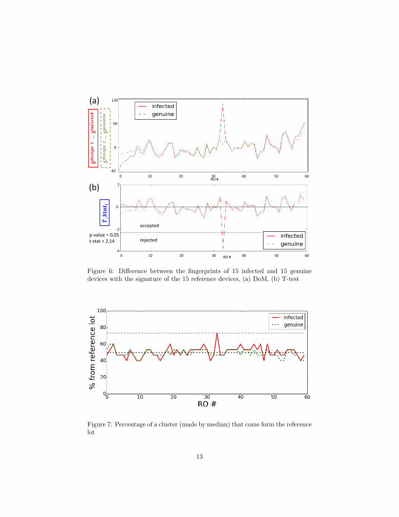
The detection method of an infected lot is similar to that of a counterfeit lot,although the alteration of the physical structure is expected to be significantlysmaller and localized. Fig. 6 shows the results obtained by applying the DoM(upper picture) and the T-test (lower picture) in order to verify the integrityof the 15 infected and 15 genuine ICs with the 15 reference ICs. 30 boardsare used. To emulate the infection (the presence of a sequential HT), a 64-bitLFSR (48 slices) has been added to the design 1. Both the DoM and the T-testallow to detect an anomaly located around RO 33 which is effectively close tothe LFSR. Moreover, the DoM stays low between the reference and the genuinelots. In this case, the absolute T-values (| T Stati |) does not exceed, 1.22 fori ∈ {1, . . . , 60}. Genuine lots are therefore recognized as uninfected lots. Similarresults have been obtained with the k-means (Fig. 8) and the median (Fig. 7).These results validate the proposed detection methodology and above all theproposed variation model of the performance of a CMOS structure in a realdesign which strongly depends on the power distribution in advanced CMOStechnologies.
12
𝑺𝑫
𝒆𝒔
𝒊𝒈𝒏
𝟏 −
𝑺𝒊𝒏
𝒇𝒆
𝒄𝒕𝒆
𝒅
𝑺𝑫
𝒆𝒔
𝒊𝒈𝒏
𝟏−
𝑺𝒈
𝒆𝒏
𝒖𝒊𝒏
𝒆
𝑻_𝑺
𝒕𝒂𝒕 𝒊
120
60
0
-60
2
0
-2
-4
p-value = 0,05 t-stat = 2,14
accepted
rejected
10 20 30 40 50 60 RO #
0
10 20 30 40 50 60 RO # 0
(b)
(a)
Figure 6: Difference between the fingerprints of 15 infected and 15 genuinedevices with the signature of the 15 reference devices, (a) DoM, (b) T-test
Figure 7: Percentage of a cluster (made by median) that come form the referencelot
13
Figure 8: Percentage of a cluster (made by kmeans) that come form the referencelot
6 Conclusion and perspectives
This paper introduces an efficient and practical approach for detecting Hard-ware Trojans in ICs and counterfeits based on a new variation model for theperformance of CMOS structures. This model gets rid of the process variationissues usually met when doing HT detection in practice. The model is actu-ally built from measurements made on ‘real circuits’ and not designs usuallydedicated to the monitoring of process variations, the latter being much moreuniform and regular in terms of physical structure and content. This approachis based on the assumption that IC infection is more likely to be done on a lotlevel than on individual isolated ICs.
A reference signature is first derived from a trusted lot (which could corre-spond in practice to a first run usually done for characterisation purposes). Thenthe same signatures will be calculated on subsequent (suspected) lots and com-pared with the reference one, using the different statistical methods describedin this paper. For counterfeit detection, we propose a way of calculating this ICfingerprint and comparing it with the reference signature. The model and themethods have been successfully experimented on a set of 30 FPGA boards asan initial validation strategy.
The next steps will be to implement the on-chip sensor structures on anASIC design and validate the method on large set of ICs. Moreover, otherfactors like the size of the HT, the density of sensors to used or the positioningof those sensors shall be investigated.
References
[1] Miron Abramovici and Paul Bradley. Integrated circuit security: Newthreats and solutions. In Proceedings of CSIIRW 2009, pages 55:1–55:3.
14
ACM.
[2] D. Agrawal, S. Baktir, D. Karakoyunlu, P. Rohatgi, and B. Sunar. Trojandetection using ic fingerprinting. In Security and Privacy, 2007. SP ’07.IEEE Symposium, pages 296–310, May 2007.
[3] J Balasch, B Gierlichs, and I Verbauwhede. Electromagnetic circuit finger-prints for hardware trojan detection. EMC 2015, IEEE, 2015.
[4] A. Bhavnagarwala, S. Kosonocky, C. Radens, K. Stawiasz, R. Mann, QiuyiYe, and Ken Chin. Fluctuation limits amp; scaling opportunities for cmossram cells. In IEDM 2005, pages 659–662, Dec 2005.
[5] K. Bowman, C. Tokunaga, J. Tschanz, A. Raychowdhury, M. Khellah,B. Geuskens, Shih-Lien Lu, P. Aseron, T. Karnik, and V. De. Dynamicvariation monitor for measuring the impact of voltage droops on micropro-cessor clock frequency. In CICC, 2010 IEEE, pages 1–4, Sept 2010.
[6] Yuan Cao, Chip-Hong Chang, and Shoushun Chen. Cluster-based dis-tributed active current timer for hardware trojan detection. In ISCAS,2013 IEEE International Symposium, pages 1010–1013, May 2013.
[7] RajatSubhra Chakraborty and Swarup Bhunia. Security against hardwaretrojan attacks using key-based design obfuscation. Journal of ElectronicTesting, 27(6):767–785, 2011.
[8] RajatSubhra Chakraborty, Francis Wolff, Somnath Paul, Christos Pa-pachristou, and Swarup Bhunia. Mero: A statistical approach for hard-ware trojan detection. In Christophe Clavier and Kris Gaj, editors, CHES2009, volume 5747 of Lecture Notes in Computer Science, pages 396–410.Springer Berlin Heidelberg, 2009.
[9] Franck Courbon, Philippe Loubet-Moundi, Jacques J.A. Fournier, and As-sia Tria. A high efficiency hardware trojan detection technique based onfast sem imaging. In In the proceedings of DATE’15, March 2015.
[10] Morris H. DeGroot and Mark J. Schervish. Probability and Statistics (4thEdition). Pearson, 2011.
[11] Andrew Ferraiuolo, Xuehui Zhang, and Mohammad Tehranipoor. Experi-mental analysis of a ring oscillator network for hardware trojan detectionin a 90nm ASIC. Proceedings of the ICCAD ’12, page 37, 2012.
[12] Ali Keshavarzi, Gerhard Schrom, Stephen Tang, Sean Ma, Keith Bowman,Sunit Tyagi, Kevin Zhang, Tom Linton, Nagib Hakim, Steven Duvall, JohnBrews, and Vivek De. Measurements and modeling of intrinsic fluctuationsin mosfet threshold voltage. In Proceedings of ISLPED 2005, pages 26–29,New York, NY, USA, 2005. ACM.
15
[13] C. Lamech, R.M. Rad, M. Tehranipoor, and J. Plusquellic. An experimen-tal analysis of power and delay signal-to-noise requirements for detectingtrojans and methods for achieving the required detection sensitivities. In-formation Forensics and Security, IEEE Transactions on, 6(3):1170–1179,Sept 2011.
[14] Jie Li and J. Lach. At-speed delay characterization for ic authenticationand trojan horse detection. In HOST 2008, pages 8–14, June 2008.
[15] Chen-Wei Liu and Yao-Wen Chang. Floorplan and power/ground networkco-synthesis for fast design convergence. In Proceedings of ISPD 2006,pages 86–93, New York, NY, USA, 2006. ACM.
[16] S. Narasimhan, Dongdong Du, R.S. Chakraborty, S. Paul, F. Wolff, C. Pa-pachristou, K. Roy, and S. Bhunia. Multiple-parameter side-channel anal-ysis: A non-invasive hardware trojan detection approach. In HOST 2010,pages 13–18, June 2010.
[17] Bettina Rebaud, Marc Belleville, Edith Beigne, Christian Bernard, MichelRobert, Philippe Maurine, and Nadine Azemard. Timing slack monitoringunder process and environmental variations: Application to a DSP perfor-mance optimization. Microelectronics Journal, 42(5):718–732, 2011.
[18] Seyed Mohammad Hossein Shekarian and Morteza Saheb Zamani. A trust-driven placement approach: A new perspective on design for hardwaretrust. Journal of Circuits, Systems and Computers, 0(0):1550115, 0.
[19] O. Soll, T. Korak, M. Muehlberghuber, and M. Hutter. Em-based detectionof hardware trojans on fpgas. In HOST 2014, pages 84–87.
[20] F. Stellari, Peilin Song, and H.A. Ainspan. Functional block extractionfor hardware security detection using time-integrated and time-resolvedemission measurements. In VTS, 2014 IEEE 32nd, pages 1–6, 2014.
[21] M. Tehranipoor and F. Koushanfar. A survey of hardware trojan taxonomyand detection. Design Test of Computers, IEEE, 27(1):10–25, Jan 2010.
[22] Kan Xiao and M. Tehranipoor. Bisa: Built-in self-authentication for pre-venting hardware trojan insertion. In HOST 2013, pages 45–50, June 2013.
[23] NGO Xuan Thuy, Najm Zakaria, Shivam Bhasin, Guilley Sylvain, andDanger Jean-luc. Method taking into account process dispersions to detecthardware trojan horse by side-channel. June 2015.
[24] Xuehui Zhang and M. Tehranipoor. Ron: An on-chip ring oscillator networkfor hardware trojan detection. In DATE 2011, pages 1–6, March 2011.