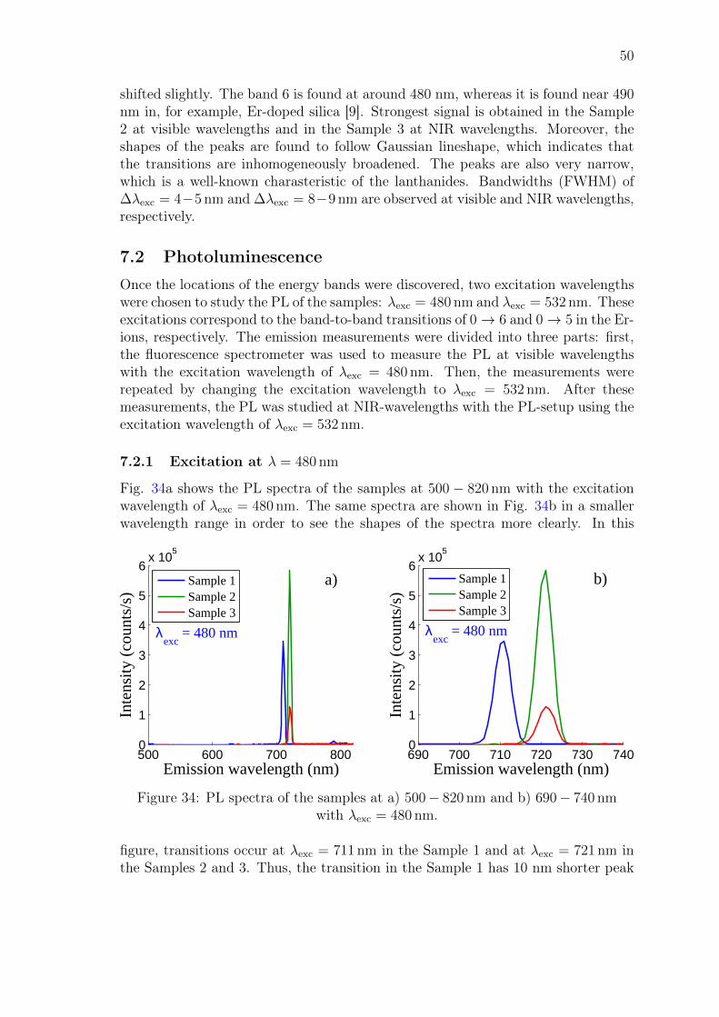
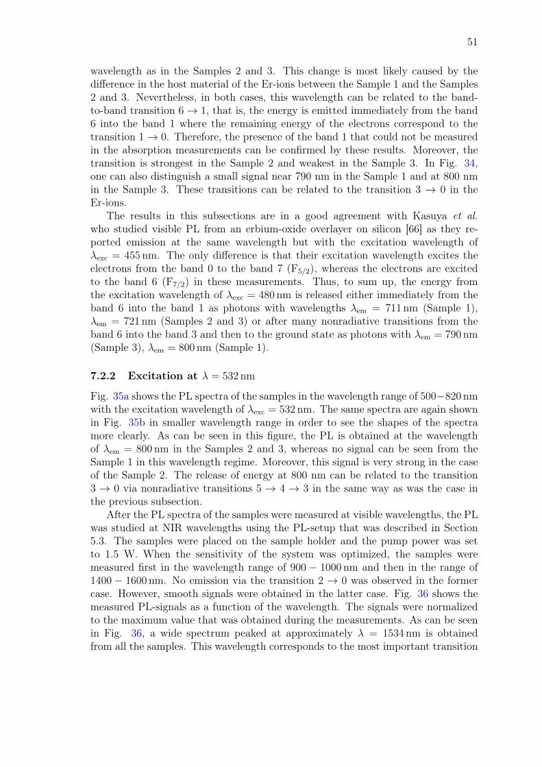
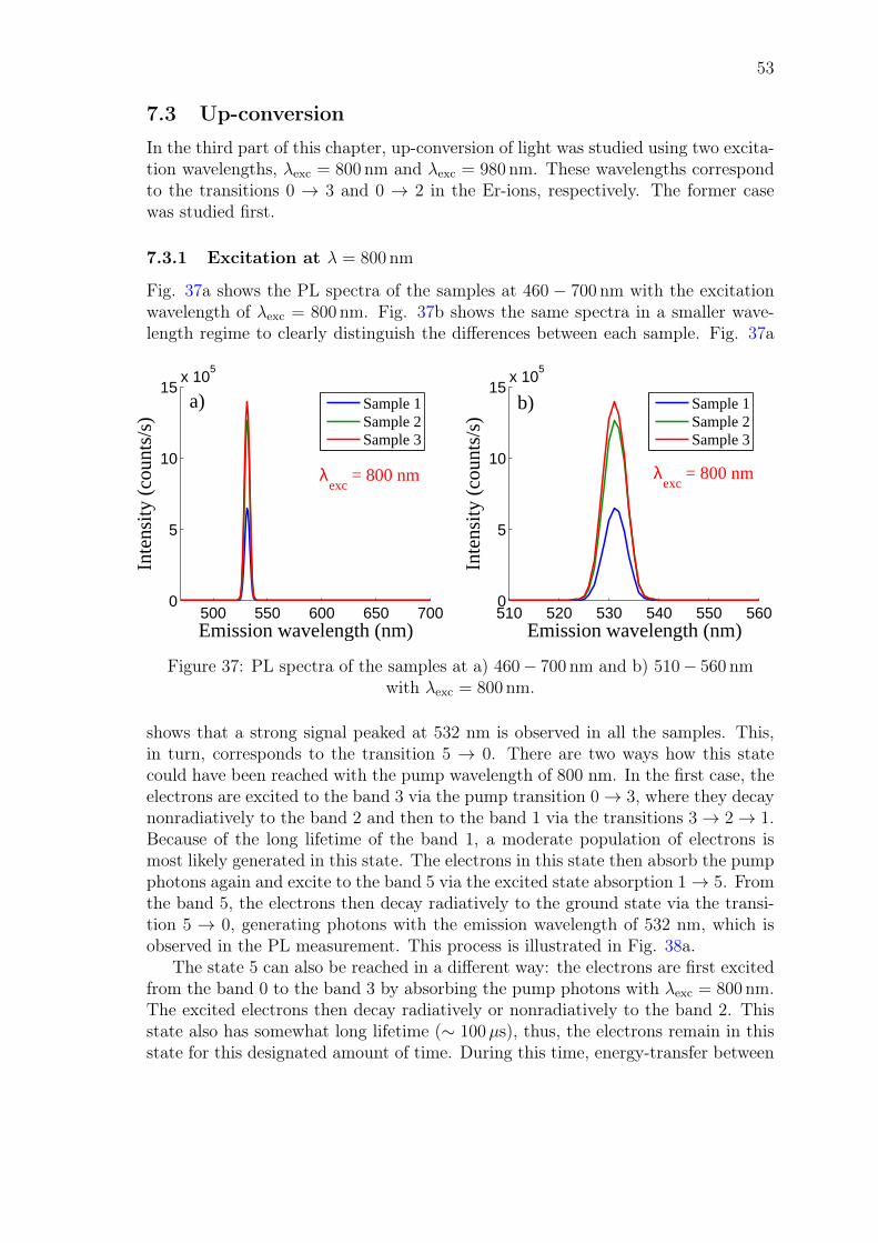
John Rönn Fabrication and characterization of atomic-layer-deposited Er 2 O 3 for optical amplifier devices School of Electrical Engineering Thesis submitted for examination for the degree of Master of Science in Technology. Espoo December 1, 2014 Thesis supervisor: Prof. Zhipei Sun Thesis advisor: D.Sc. (Tech.) Lasse Karvonen
Transcript
John Rönn
Fabrication and characterization ofatomic-layer-deposited Er2O3 for opticalamplifier devices
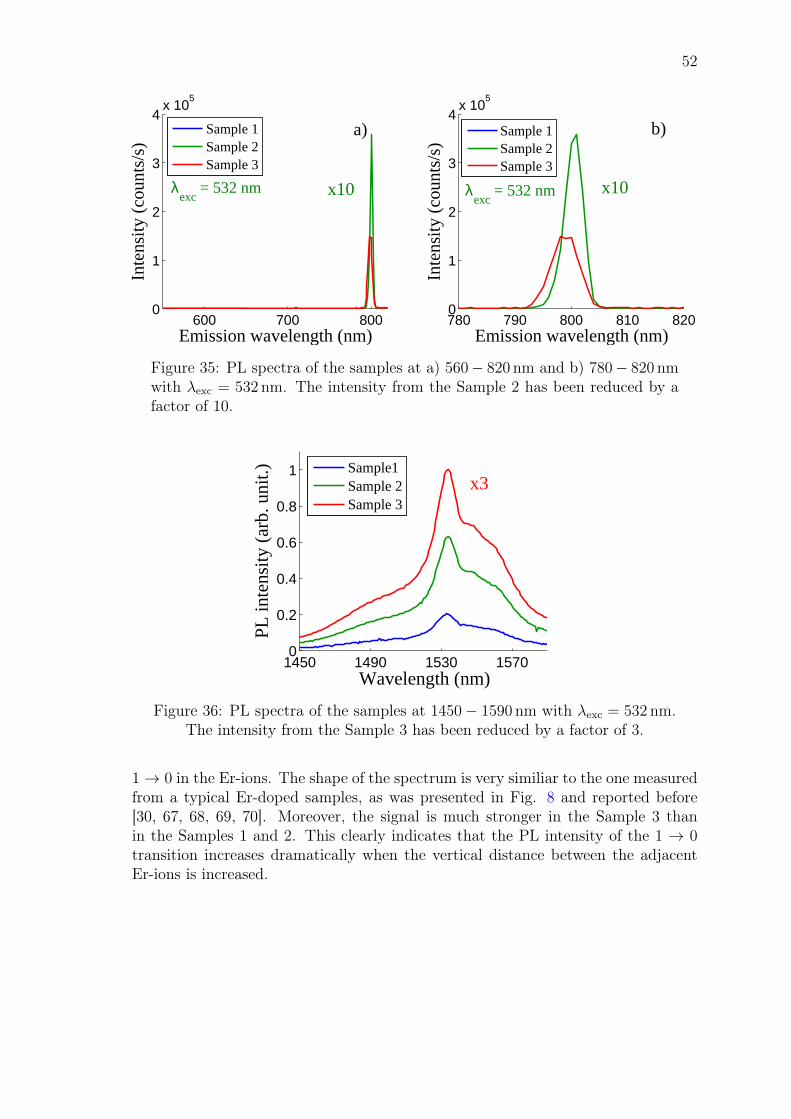
School of Electrical Engineering
Thesis submitted for examination for the degree of Master ofScience in Technology.Espoo December 1, 2014
Thesis supervisor:
Prof. Zhipei Sun
Thesis advisor:
D.Sc. (Tech.) Lasse Karvonen
aalto universityschool of electrical engineering
abstract of themaster’s thesis
Author: John Rönn
Title: Fabrication and characterization of atomic-layer-deposited Er2O3 foroptical amplifier devices
Date: December 1, 2014 Language: English Number of pages: 7+64
Department of Micro- and nanotechnology
Professorship: Micro- and nanotechnology Code: S3010
Supervisor: Prof. Zhipei Sun
Advisor: D.Sc. (Tech.) Lasse Karvonen
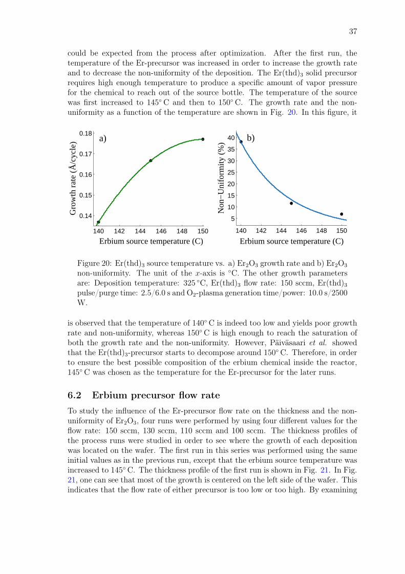
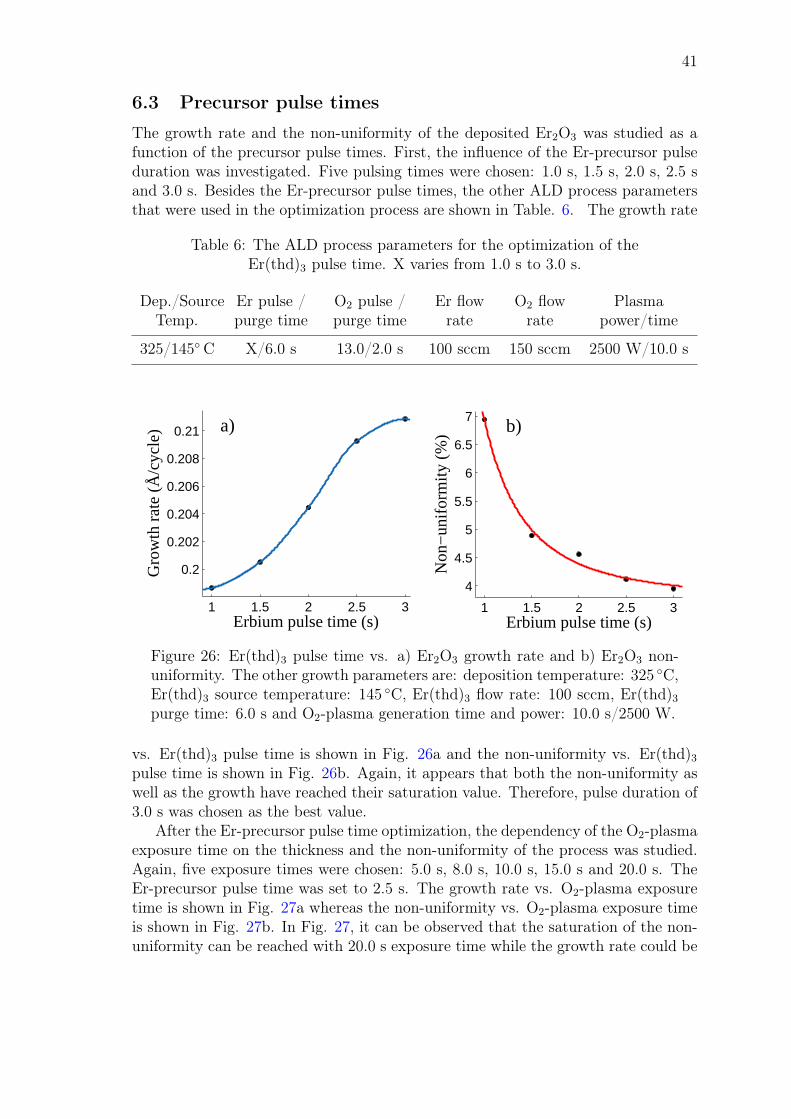
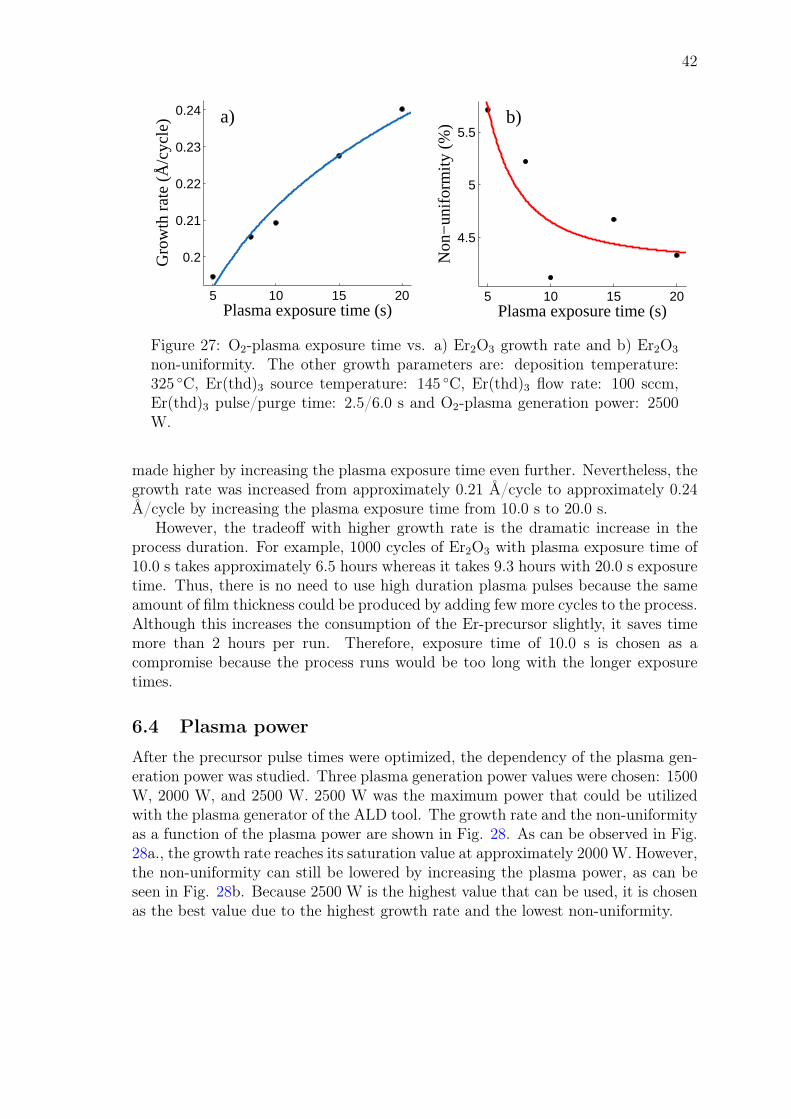
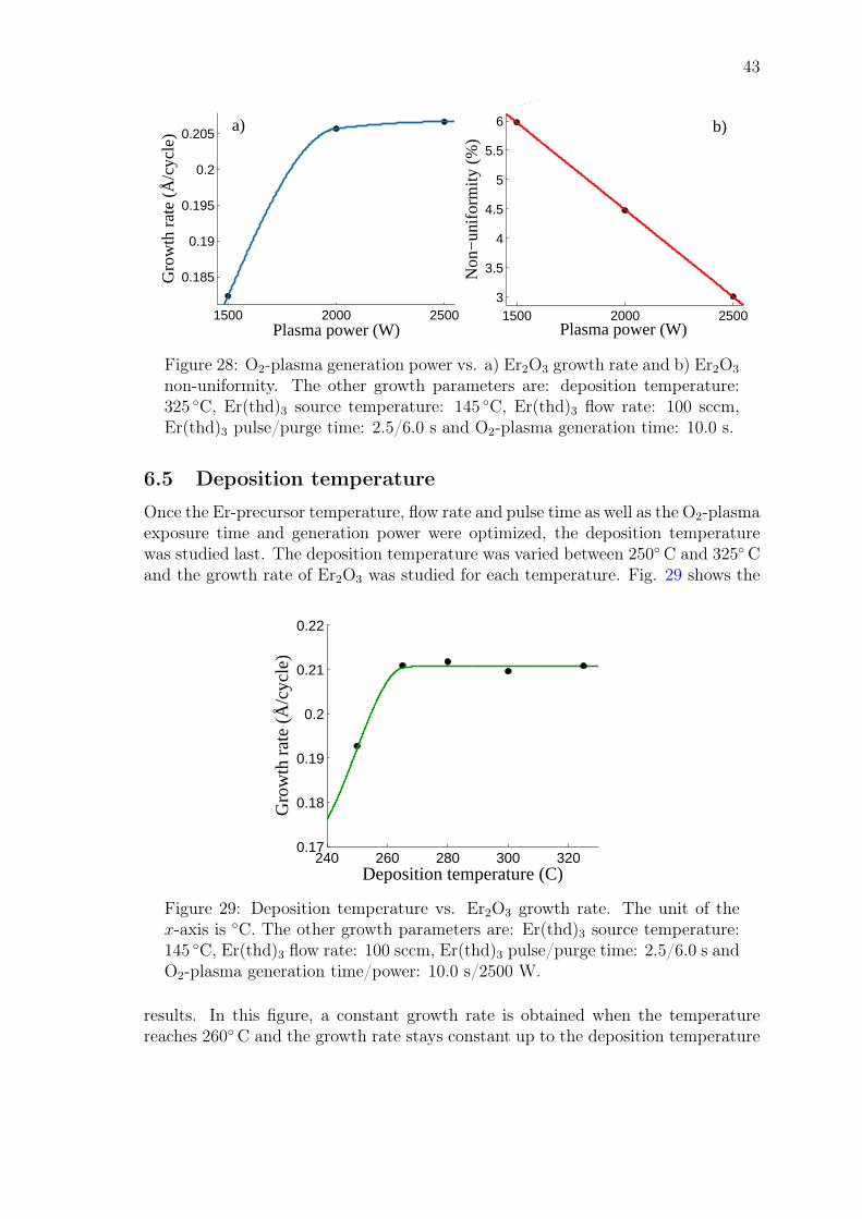
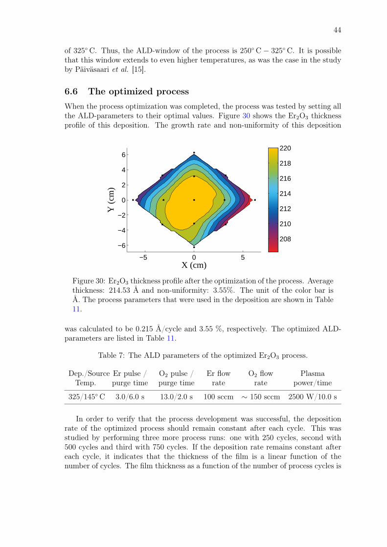
Recently, erbium-doped optical amplifiers have drawn significant attention as asolution to compensate the propagation losses for silicon photonics due to theirability to produce amplification of light at λ = 1.5µm with high efficiency andlow noise over wide bandwidth. In silicon photonics, much effort has been putinto the development of Er-doped optical amplifiers in the form of strip or slotwaveguides, in which the amplification is produced over short (∼ cm) structures.However, there has not been any major success in the development, because sev-eral challenges arise in Er-doped waveguide amplifiers as the amplification overshort structures requires very high concentration of Er-ions in the amplifier gainmaterial. It has been shown that some of these challenges can be avoided by opti-mizing the fabrication of the Er-doped gain material. Atomic layer deposition hasshown a great potential in the fabrication of Er-doped materials because it can beused to precisely control the profile of the Er-ions in the amplifier gain material.In this thesis, plasma-enhanced atomic layer deposition has been successfullyused to fabricate Er-doped materials and to control their photoluminescence atλ = 1.5µm. This was done in two parts. First, an optimized ALD process forerbium in its sesquioxide form, Er2O3, was developed and as a result, a growthrate of 0.215 Å/cycle and non-uniformity of 3.55 % were obtained on 6" wafer.Er2O3 was then deposited in a nanolaminate configuration with Al2O3 and thethickness of the Al2O3 was controlled. The as-deposited samples were then op-tically characterized with absorption and photoluminescence measurements andit was observed that when the thickness of the Al2O3-layer between the Er2O3-layers was increased, an enhanced photoluminescence signal at λ = 1.5µm wasmeasured. Therefore, this thesis shows that the photoluminescence of the Er-ions at λ = 1.5µm can be greatly enhanced by the nanoscale engineering of thefabrication process.
Työn nimi: Atomikerroskasvatetun Er2O3:n valmistaminen ja senkarakterisointi optisia vahvistinlaitteita varten
Päivämäärä: December 1, 2014 Kieli: Englanti Sivumäärä: 7+64
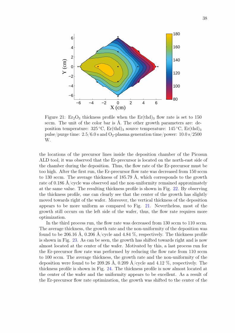
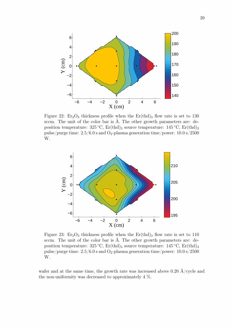
Mikro- ja nanotekniikan laitos
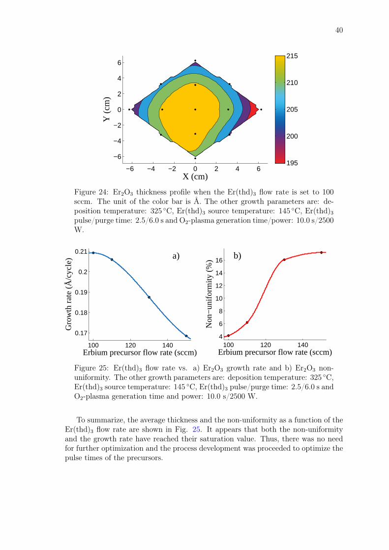
Professuuri: Mikro- ja nanotekniikka Koodi: S3010
Valvoja: Prof. Zhipei Sun
Ohjaaja: TkT Lasse Karvonen
Erbium-seostetut materiaalit ovat herättäneet kiinnostusta potentiaalisina ma-teriaaleina valon vahvistamiseen ja valonlähteiksi piifotoniikassa. Piifotoniikassavalon teho vaimenee sekä sirujen välisissä kytkennöissä, että itse valokanavissa jatämän takia signaalia täytyy vahvistaa. Myös halpojen, helposti integroitavienvalonlähteiden puute on merkittävä ongelma piifotoniikassa. Jotta signaalinvavistus piipohjaisissa valokanavarakenteissa pystyttäisiin toteuttamaan, erbium-seostettuja materiaaleja on pyritty yhdistämään piifotoniikkaan. Valokanavissatörmätään kuitenkin erilaisiin haasteisiin, koska erbium-ionien määrää täytyy kas-vattaa radikaalisti vahvistuksen aikaansaamiseksi lyhyillä matkoilla. Tästä syystälisää tutkimusta ja uusia valmistustekniikoita tarvitaan erbium-pohjaisten valo-kanavavahvistimien toteuttamiseksi. Atomikerroskasvatusmenetelmä on erityisenpotentiaalinen menetelmä erbium-pohjaisten materiaalien valmistamiseen, koskasillä voidaan tarkasti säätää erbium-ionien jakaumaa vahvistimen sisällä.Tässä työssä on pystytty näyttämään, että plasma-avustettua atomikerroskasva-tusmenetelmää voidaan käyttää erbium-seostettujen materiaalien valmistamisessaja niiden optisten ominaisuuksien säätämisessä Al2O3-pohjaisissa näytteissä.Tämä tavoite saavutettiin kahdessa osassa. Ensimmäisessä osassa kehitettiin op-timoitu prosessi erbiumoksidille (Er2O3). Kyseisen Er2O3-prosessin kasvunopeu-den ja epätasaisuuden mitattiin olevan 0.215 Å/sykli ja 3.55 % kuuden tuumankiekolla. Seuraavaksi alumiinioksidia seostettiin erbiumilla kasvattamalla Er2O3-kerroksia alumiinioksidikerrosten väliin. Materiaalin ominaisuuksia pystyttiinkontrolloimaan muuttamalla alumiinioksidikerroksen paksuutta Er2O3-kerroksenvälillä. Optisissa mittauksissa huomattiin, että kun alumiinioksidikerroksenpaksuus kasvoi, myös fotoluminesenssi 1.5µm:n aallonpituudella kasvoi. Työtäten osoitti, että erbium-ionien fotoluminesenssiä voidaan tehostaa optimoimallaerbium-ionien valmistusmenetelmää.
PrefaceThis thesis contains a lot of fabrication and characterization and therefore, manypeople have helped me during the process. First and foremost, I would like to thankmy instructor Lasse Karvonen, who has not only instructed me in this thesis, butwho has helped me with everything since the second year of my studies. I would alsolike to thank Sami Kujala and Seppo Honkanen, who instructed me in my Bachelor’sstudies intensively.
I would like to say many thanks to my advisor and professor, Zhipei Sun, wholet me personally decide the topic of this thesis and who has backed up my decisionssince he joined the Aalto University. I hope I can continue to work in Zhipei’s groupas a postgraduate student in the future.
In addition, special thanks are given to Antti Säynätjoki, who explained manythings related to this thesis, to Henri Jussila and Jukka Hassinen who helped withwith the optical measurements and to Alex Perros, Perttu Sippola and Ville Rontuwho helped me with the ALD-processing.
Finally, I want to express my gratitude to my friends and family and to mybeloved girlfriend Meri, to whom I fell in love during this thesis.
SymbolsE Energyω Angular frequency of lightω0 Resonance (center) frequency of lightλ Wavelength (in general)λc Resonance (center) wavelengthλexc Excitation wavelengthλem Emission wavelength∆λ Bandwidth (FWHM)~ω Energy of a photon with angular frequency ωσ21 Emission cross-sectionσ12 Absorption cross-section
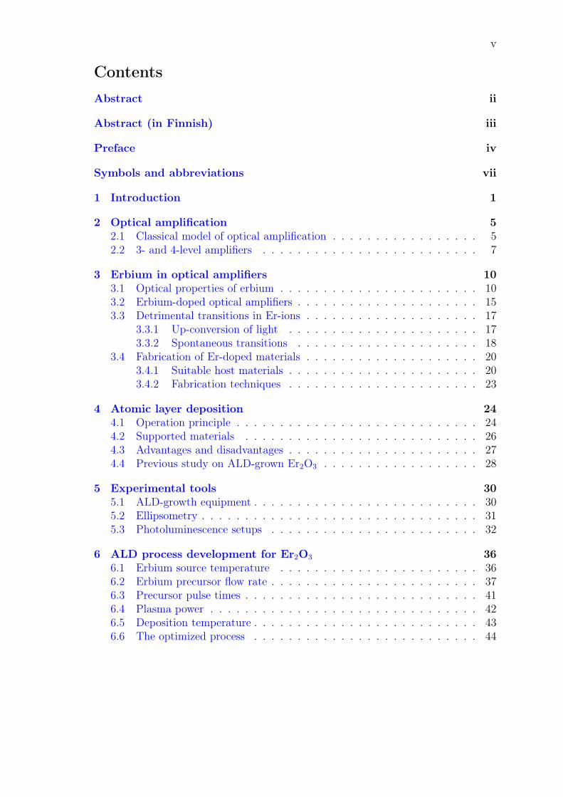
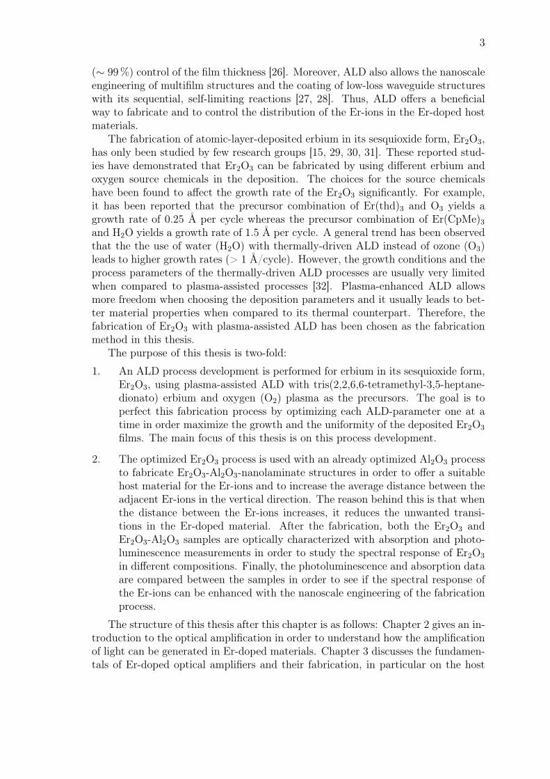
1 IntroductionLight is electromagnetic radiation that can be found almost everywhere in the world.It is one of the most important physical phenomenom that can be used in variousways either in technology or simply in nature. In technology, one way to utilizelight is to transfer information. Light travels as short pulses in optical networkswhere it is guided by optical fibers to its destination [1]. The core material ofoptical fibers is pure silica which can offer very low absorption to the signal lightif the wavelength is chosen correctly. Modern telecommunication networks use λ =1.55µm as the signal wavelength because the absorption of silica has its lowest valuearound this wavelength. This wavelength regime is often referred to as the thirdtransparency window of silica [2]. In this transparency window, the attenuation isonly limited by the Rayleigh scattering of light, as illustrated in Fig. 1 that shows theabsorption spectrum of a commercial silica optical fiber [3]. The optical attenuation
800 1000 1200 1400 1600 1800
1
2
3
4
5
Wavelength (λ)
Atte
nuat
ion
(dB
/km
)
3rd transparencywindow
Impurity absorptionRayleigh scattering
IR−absorption
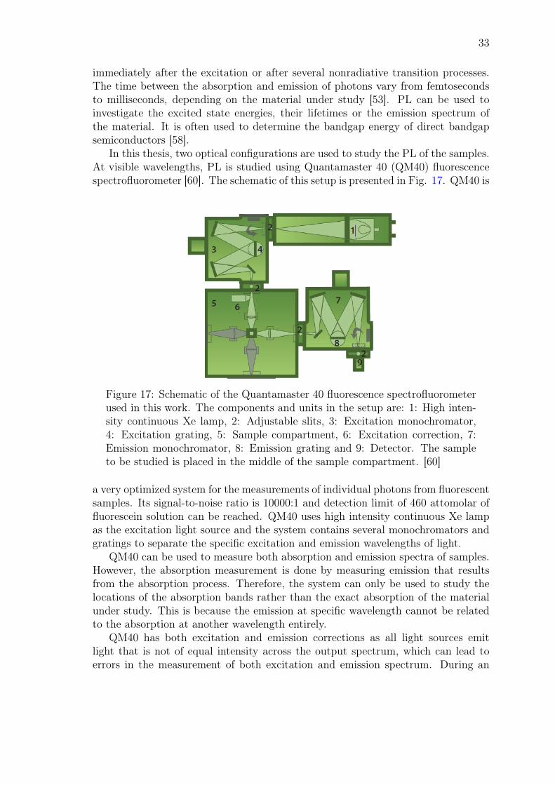
Figure 1: The attenuation spectrum of a commercial optical fiber. The atten-uation is dominated by the Rayleigh scattering in the visible-NIR wavelengthsand by optical absorption in the IR wavelengths. The attenuation is minimumat around λ = 1.55µm. Data from [3].
of this fiber can be made as small as 0.2 dB/km, which has enabled large amount ofdata to be sent in the optical networks. For example, today’s internet connectionscan easily reach transfer rates of gigabits per second (Gbit/s) [4]. Moreover, theoptical networks offer acceptable bit error rate even in large networks and they arenowadays used in long-distance telephone networks, high-density metropolitan areasand in cable-television trunk lines [5]. However, a problem rises in the large opticalnetworks because the signal to be transferred still experiences moderate amount ofloss (> 2 dB) after long-haul distances (> 10 km). The best solution to this problemis to use an optical amplifier which can compensate the losses that arise in theselarger communication networks.
2
In photonics, there are three main types of optical amplifiers one can use toamplify light: rare-earth doped amplifiers, semiconductor amplifiers and Ramanamplifiers [4]. Rare-earth doped amplifiers, especially rare-earth doped fiber am-plifiers have been studied extensively because rare-earth elements possess uniqueoptical properties [6]. When embedded in a proper host material, rare-earth ionscan emit light with either very narrow or wide bandwidth in the visible and infraredspectrum [7]. Moreover, this emission can be controlled by the host material inwhich the rare-earth ions are doped [8]. Erbium (Er), which is one of the 17 rare-earth elements, has an emission band that coincides with the absorption minimum ofcommercial optical fibers. Because of this, much work has been put into the study oferbium as the gain material for the optical fiber amplifiers [5]. As a result, Er-dopedfiber amplifiers (EDFAs) have been invented and they are nowadays a crucial partof the modern telecommunication networks [9].
Owing to the success of EDFAs, it is of great technological interest to bring theEr-doped amplifiers into micrometer sized photonic circuits that use light insteadof electrical current to transfer information [10]. In photonics applications, espe-cially in silicon photonics and integrated optics, most of the signal that travels inthe optical waveguides is lost when the light is coupled into and between the in-tegrated circuit chips. Therefore, Er-doped waveguide amplifiers (EDWAs) mightenable new generation devices along with microelectronics because they can be usedto amplify the light that is otherwise lost in the on-chip and chip-to-chip intercon-nects [11]. In future, this could possibly bring all the required functions of multipleoptoelectronical devices into a single chip, thus, reducing the size and cost of modernoptoelectronical systems greatly [12].
Although erbium has been widely studied in the association with optical fibersand fiber amplifiers, more knowledge is needed when the Er-doped amplifiers areintegrated with optical waveguides. In the case of EDWAs, the amplification mustbe carried over much shorter lengths (∼ cm), thus, requiring higher Er-ion concen-trations than in the case of traditional fiber amplifiers in order to achieve reasonableamplification [13]. This brings two major challenges in the operation and fabrica-tion of the EDWAs: First, typical glass materials cannot contain high concentrationof Er-ions without clustering, and second, the ion-ion interactions create unwantedtransitions that lead to reduced gain and increased noise in the Er-doped amplifier[14]. In order to answer these challenges and to ensure the best possible operation ofthe Er-doped waveguide amplifiers, the distribution of the Er-ions in the amplifierdevice has to be controlled. Therefore, a delicate care has to be invested in thefabrication technique of the Er-doped materials.
Er-doped materials can be grown using various methods, including atomic layerdeposition [15], dip-coating [16], flame hydrolysis [17], high-vacuum chemical vapourdeposition [18], plasma-enhanced chemical vapour deposition [19], pulsed laser de-position [20], reactive co-sputtering [21], RF-sputtering [22], sol-gel method [23],spin coating [24] and vapour phase deposition [25]. Of these fabrication methods,atomic layer deposition (ALD) is of the great interest because it possesses uniquedeposition properties that no other technique holds. For example, ALD is capa-ble of producing thin films with very high conformality, aspect ratio and accurate
3
(∼ 99 %) control of the film thickness [26]. Moreover, ALD also allows the nanoscaleengineering of multifilm structures and the coating of low-loss waveguide structureswith its sequential, self-limiting reactions [27, 28]. Thus, ALD offers a beneficialway to fabricate and to control the distribution of the Er-ions in the Er-doped hostmaterials.
The fabrication of atomic-layer-deposited erbium in its sesquioxide form, Er2O3,has only been studied by few research groups [15, 29, 30, 31]. These reported stud-ies have demonstrated that Er2O3 can be fabricated by using different erbium andoxygen source chemicals in the deposition. The choices for the source chemicalshave been found to affect the growth rate of the Er2O3 significantly. For example,it has been reported that the precursor combination of Er(thd)3 and O3 yields agrowth rate of 0.25 Å per cycle whereas the precursor combination of Er(CpMe)3
and H2O yields a growth rate of 1.5 Å per cycle. A general trend has been observedthat the the use of water (H2O) with thermally-driven ALD instead of ozone (O3)leads to higher growth rates (> 1 Å/cycle). However, the growth conditions and theprocess parameters of the thermally-driven ALD processes are usually very limitedwhen compared to plasma-assisted processes [32]. Plasma-enhanced ALD allowsmore freedom when choosing the deposition parameters and it usually leads to bet-ter material properties when compared to its thermal counterpart. Therefore, thefabrication of Er2O3 with plasma-assisted ALD has been chosen as the fabricationmethod in this thesis.
The purpose of this thesis is two-fold:
1. An ALD process development is performed for erbium in its sesquioxide form,Er2O3, using plasma-assisted ALD with tris(2,2,6,6-tetramethyl-3,5-heptane-dionato) erbium and oxygen (O2) plasma as the precursors. The goal is toperfect this fabrication process by optimizing each ALD-parameter one at atime in order maximize the growth and the uniformity of the deposited Er2O3
films. The main focus of this thesis is on this process development.
2. The optimized Er2O3 process is used with an already optimized Al2O3 processto fabricate Er2O3-Al2O3-nanolaminate structures in order to offer a suitablehost material for the Er-ions and to increase the average distance between theadjacent Er-ions in the vertical direction. The reason behind this is that whenthe distance between the Er-ions increases, it reduces the unwanted transi-tions in the Er-doped material. After the fabrication, both the Er2O3 andEr2O3-Al2O3 samples are optically characterized with absorption and photo-luminescence measurements in order to study the spectral response of Er2O3
in different compositions. Finally, the photoluminescence and absorption dataare compared between the samples in order to see if the spectral response ofthe Er-ions can be enhanced with the nanoscale engineering of the fabricationprocess.
The structure of this thesis after this chapter is as follows: Chapter 2 gives an in-troduction to the optical amplification in order to understand how the amplificationof light can be generated in Er-doped materials. Chapter 3 discusses the fundamen-tals of Er-doped optical amplifiers and their fabrication, in particular on the host
4
material selection. Chapter 4 focuses on the operation principle and properties ofALD and Chapter 5 describes the experimental tools that have been used in thisthesis. Chapter 6 presents my results on the Er2O3 process development and inChapter 7, my results from the optical measuements of the as-deposited Er2O3 andEr2O3-Al2O3 samples are presented and discussed thoroughly. Chapter 8 concludesthis thesis with a brief summary as well as an outlook of the topic.
5
2 Optical amplificationThe previous chapter explained why erbium is needed in the optical networks as apart of the amplifier design. In order to understand the physical phenomena behindthese amplifiers and what exactly makes erbium so special material, it is mandatoryto know how light can be generated and how it is amplified. Therefore, this chapterintroduces the physical principles of the optical amplification and explains how it isgenerated in typical amplifier devices.
2.1 Classical model of optical amplification
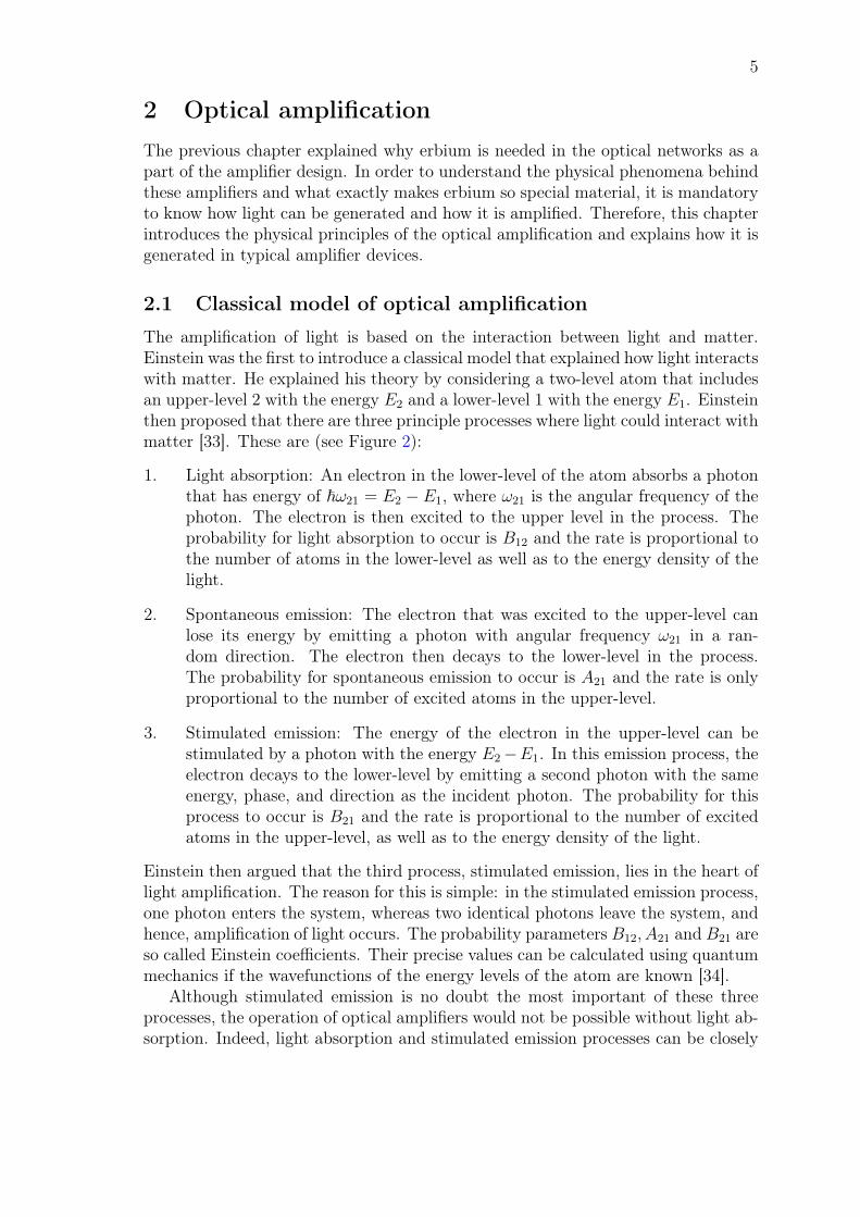
The amplification of light is based on the interaction between light and matter.Einstein was the first to introduce a classical model that explained how light interactswith matter. He explained his theory by considering a two-level atom that includesan upper-level 2 with the energy E2 and a lower-level 1 with the energy E1. Einsteinthen proposed that there are three principle processes where light could interact withmatter [33]. These are (see Figure 2):
1. Light absorption: An electron in the lower-level of the atom absorbs a photonthat has energy of ~ω21 = E2 − E1, where ω21 is the angular frequency of thephoton. The electron is then excited to the upper level in the process. Theprobability for light absorption to occur is B12 and the rate is proportional tothe number of atoms in the lower-level as well as to the energy density of thelight.
2. Spontaneous emission: The electron that was excited to the upper-level canlose its energy by emitting a photon with angular frequency ω21 in a ran-dom direction. The electron then decays to the lower-level in the process.The probability for spontaneous emission to occur is A21 and the rate is onlyproportional to the number of excited atoms in the upper-level.
3. Stimulated emission: The energy of the electron in the upper-level can bestimulated by a photon with the energy E2−E1. In this emission process, theelectron decays to the lower-level by emitting a second photon with the sameenergy, phase, and direction as the incident photon. The probability for thisprocess to occur is B21 and the rate is proportional to the number of excitedatoms in the upper-level, as well as to the energy density of the light.
Einstein then argued that the third process, stimulated emission, lies in the heart oflight amplification. The reason for this is simple: in the stimulated emission process,one photon enters the system, whereas two identical photons leave the system, andhence, amplification of light occurs. The probability parameters B12, A21 and B21 areso called Einstein coefficients. Their precise values can be calculated using quantummechanics if the wavefunctions of the energy levels of the atom are known [34].
Although stimulated emission is no doubt the most important of these threeprocesses, the operation of optical amplifiers would not be possible without light ab-sorption. Indeed, light absorption and stimulated emission processes can be closely
6
E1
E2
E2 E1-
E E2E
E1
E2 E1-
E2E
E1
E2E
E1
E2E
E1
E2 E1-
E 2
E 1-
2x
a) b) c)
Figure 2: Interaction processes between light and matter; a) Light absorption, b)Spontaneous emission and c) Stimulated emission.
related to each another. It turns out that the probabilities for both processes tooccur are equally likely, that is, B21 = B12 if the upper- and lower-levels have thesame degeneracy. This means that in normal conditions, the absorption and stimu-lated emission will compete against each other. Thus, the net gain or amplificationis only dependent on the number of atoms in the upper- and lower-levels. [35]
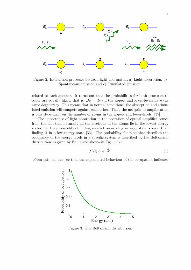
The importance of light absorption in the operation of optical amplifier comesfrom the fact that naturally all the electrons in the atoms lie in the lowest-energystates, i.e. the probability of finding an electron in a high-energy state is lower thanfinding it in a low-energy state [33]. The probability function that describes theoccupancy of the energy levels in a specific system is described by the Boltzmanndistribution as given by Eq. 1 and shown in Fig. 3 [36]:
f(E) ∝ e−EkT . (1)
From this one can see that the exponential behaviour of the occupation indicates
0 1 2 3 4 50
0.2
0.4
0.6
0.8
1
Energy (a.u.)
Prob
abili
ty o
f oc
cupa
tion
Figure 3: The Boltzmann distribution.
7
that the rate of stimulated emission will be vanishingly small in room tempera-ture, because there are not enough excited atoms that can be stimulated to emitradiation. In order to increase the rate of stimulated emission to produce light am-plification, the electrons must be excited to the upper level by an external pumpsource. The pumping is usually done optically, that is, using a laser source thatexcites the electrons by light absorption. Once the upper-level holds more electronsthan the lower-level, the situation is called as population inversion [35]. The excitedupper-level electrons can be then stimulated to produce photons and to realize lightamplification.
2.2 3- and 4-level amplifiers
The principle operation of an optical amplifier is to produce gain. In a two-levelatomic system that Einstein proposed, the amplification of light would occur whenthe rate of stimulated emission exceeded the rate of light absorption. This occurswhen the number of atoms in the upper-level becomes higher than the number ofatoms in the lower-level or in other words, when the population inversion is reached.It turns out that this kind of system cannot produce light amplification or gain,because the maximum number of excited atoms is half of the total number of atomsin the system [37]. The reason lies in the fact that when the number of atoms in theupper-level becomes equal to the number of atoms in the lower-level, the probabilityfor stimulated emission to occur is half, whereas the probability of light absorptionto occur is also half. That is, when atom is excited to the upper-level, the chanceof releasing an electron from the upper-level is equally likely. Because of this, mostlasers and amplifiers operate using so-called three- and four-level configurations [35].
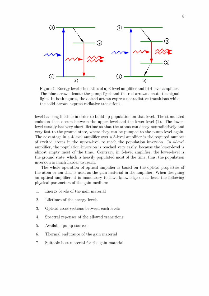
Figure 4a shows the energy level schematic of a three-level amplifier. This config-uration consists of three energy-levels: a ground state (1), a pump-level (3) and anupper-level (2). In equilibrium, the ground state holds most of the atoms, whereasthe pump-level holds the lowest amount of atoms because of the Boltzmann statis-tics. In a working 3-level amplifier, the atoms are excited to the pump-level wherethey decay nonradiatively and very fast to the upper-level, creating population in-version between that level and the ground state. The lifetime of the upper-level isusually very long so that the population can build fast to achieve the populationinversion. The excited atoms in the upper-level can be then released as stimulatedemission to produce amplification for light that has energy equal to the energy dif-ference between the upper-level and the ground state. The three-level amplifier hasmany advantages. First of all, in a three-level amplifier, the pump and signal lightshave different wavelengths, thus, one avoids the re-absorption of the signal light tothe upper-level. Secondly, the absorption spectrum of the pump transition is usuallymade very broad so that one can excite atoms in the ground state with spectrallywide pump sources [38].
Figure 4b shows an example of a 4-level amplifier. The configuration is almostsame as in a 3-level amplifier except that there is now an additional level betweenthe ground state and the upper-level. The atoms are first excited to the pump level(4), where they again decay nonradiatively and very fast to the upper-level (3). This
8
22
3
1
22
3
1
3
4
11
2222
a) b)
Figure 4: Energy level schematics of a) 3-level amplifier and b) 4-level amplifier.The blue arrows denote the pump light and the red arrows denote the signallight. In both figures, the dotted arrows express nonradiative transitions whilethe solid arrows express radiative transitions.
level has long lifetime in order to build up population on that level. The stimulatedemission then occurs between the upper level and the lower level (2). The lower-level usually has very short lifetime so that the atoms can decay nonradiatively andvery fast to the ground state, where they can be pumped to the pump level again.The advantage in a 4-level amplifier over a 3-level amplifier is the required numberof excited atoms in the upper-level to reach the population inversion. In 4-levelamplifier, the population inversion is reached very easily, because the lower-level isalmost empty most of the time. Contrary, in 3-level amplifier, the lower-level isthe ground state, which is heavily populated most of the time, thus, the populationinversion is much harder to reach.
The whole operation of optical amplifier is based on the optical properties ofthe atom or ion that is used as the gain material in the amplifier. When designingan optical amplifier, it is mandatory to have knowledge on at least the followingphysical parameters of the gain medium:
1. Energy levels of the gain material
2. Lifetimes of the energy levels
3. Optical cross-sections between each levels
4. Spectral reponses of the allowed transitions
5. Available pump sources
6. Thermal endurance of the gain material
7. Suitable host material for the gain material
9
Of course, it is not easy to fulfill all the required criteria for the gain material, espe-cially when one has to consider the rarity, price and fabrication of the material also.The energy-levels of suitable gain materials may not support the 4-level amplifierconfiguration so one has to settle for a 3-level amplifier which requires much largeramounts of pump powers to produce gain. All in all, it is up to the engineer tochoose which parameters are important for specific applications.
10
3 Erbium in optical amplifiersThe previous chapter introduced the basic principles of optical amplification anddemonstrated how it is generated in optical amplifiers. This chapter presents erbiumas a gain material for the optical amplifiers and explains what makes erbium sounique material in the optical applications. In section 3.1, the atomic configurationof erbium is reviewed in order to understand its unique optical properties. Theenergy levels of erbium and the allowed transitions in the Er-ions are also presented.Section 3.2 introduces the operation principle of the Er-doped amplifiers and Section3.3 gives a detailed analysis on the detrimental effects that limit the operation ofthese amplifiers. Finally, section 3.4 focuses on the fabrication of Er-doped materialsand gives the requirements for the host materials that need to be satisfied in orderto produce functional Er-doped amplifier materials.
3.1 Optical properties of erbium
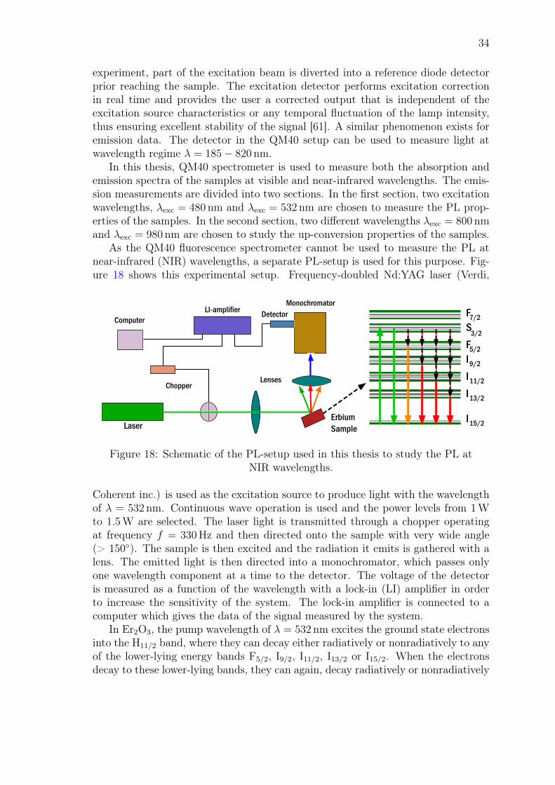
Erbium is a rare-earth metal that belongs to the group of lanthanides [39]. Thelanthanide group consists of elements with atomic numbers from 57 to 71 as shownin Figure 5, which presents the periodic table of elements. First lanthanide is lan-
Figure 5: The periodic table of the elements that shows the group of thelanthanides. [40]
thanum, then cerium and so on. The most interesting elements in this category foroptical devices are neodymium (Nd - 60), erbium (Er - 68) and ytterbium (Yb -70). It is worthwhile to note that rare-earth elements are actually not so rare; mostelements can be found in earth’s crust in moderate amounts [9]. Erbium was firstdiscovered near the village of Ytterby by Carl Gustaf Mosander in 1843. Mosandernamed one of the rare-earth elements, ytterbium, after this village and gave erbium
11
its name accordingly. Erbium and other rare-earth elements cannot be found alone;they are always part of some minerals and their extraction has been very difficultand expensive until ion-exchange methods were produced [9].
Erbium and the other lanthanides are interesting materials both physically andchemically because their atomic properties are different from those of semiconductorsor transition metals. This can be explained with their electronic configuration. Inthe classical model of atoms the atom consists of positive nucleus surrounded bynegatively charged electrons. When the atomic number Z increases, the electronshells with the lowest energies are filled first and the shells with the highest energiesare filled last. In principle, these shells have increasing radii as one moves from theinner shell all the way to the outer shell. However, starting from the element withthe atomic number Z = 57, that is, the first rare-earth metal lanthanum, the radiiof the highest-lying energy shells actually shrink and cannot obey this rule anymore[9]. To gain insight what exactly happens inside lanthanides when the radii of theouter shells start to shrink, take, for example, the electronic configuration of erbium:
1s22s22p63s23p63d104s24p64d105s25p64f126s2
or [Xe]4f126s2 where [Xe] presents the core of the element xenon. The energy statesare labeled using the spectroscopic notation [33]. The principal quantum number isgiven first, followed by the orbital quantum number as letter and the power denoteshow many electrons the specific state holds. Table 1 shows which letter matchesthe orbital quantum number, l, in the above notation. Nevertheless, erbium alone
Table 1: Orbital quantum number in spectroscopic notation.
Letter s p d f g h i
l 0 1 2 3 4 5 6
is almost always found in its trivalent state, Er3+, because its 6s electrons and one4f electron are usually removed due to their low ionization energies. The electronicconfiguration of Er3+ is [Xe]4f11, thus, the electrons in the 4f state are the valenceelectrons of the Er-ion, that is, they have the highest energy and they are responsiblefor the chemical bonding of the element. However, it turns out that the averageradius of this 4f orbital is almost twice as small as the average radii of the fully-occupied 5s and 5p orbitals [9]. This means that the valence electrons in the 4f statepenetrate deep in to the core of erbium and are, thus, shielded by the 5s and 5pelectrons [6]. As a consequence, the valence electrons cannot participate in chemicalreactions. This is the main reason why lanthanides have their own group in theperiodic table of the elements.
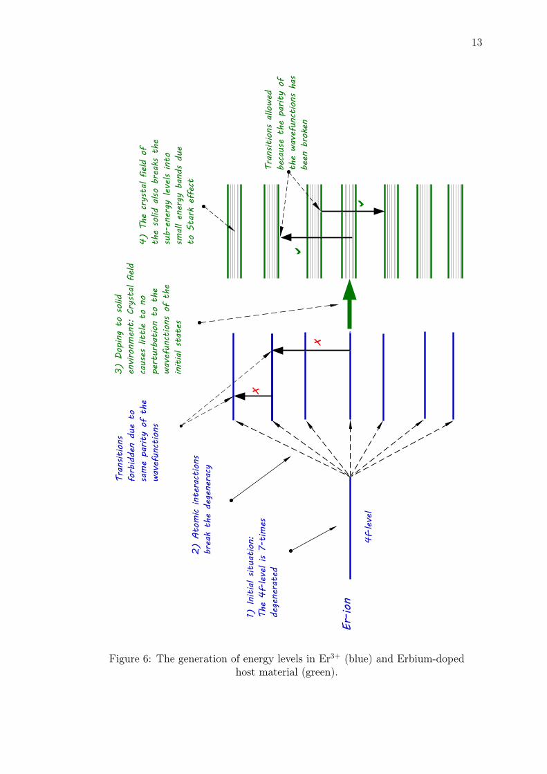
The shielding of the valence electrons gives erbium and the other lanthanidesrich optical properties that can be employed in the optical applications. In order toundestand where these unique optical properties of erbium and the other lanthanidescome from, let us take a closer look how a series of interaction processes lead to thegeneration of energy levels in the Er-ions, as illustrated in Figure 6:
12
1. The 4f energy state that holds 11 electrons is actually a combination of 2l+ 1degenerate energy levels, which corresponds to 7 degenerate energy states inthe 4f shell. Each of these levels can hold two electrons; one spin-up electronand one spin-down electron.
2. The degeneracy of the 4f level is hardly maintained because the atomic in-teractions, such as spin-orbit, orbit-orbit, spin-spin and residual electrostaticinteractions between the individual electrons break the degeneracy of the en-ergy states [38], resulting in 7 nondegenerate sub-energy levels within the 4fshell of Er3+. However, the electronic transitions within these sublevels areforbidden in Er3+ because the wavefunctions of the energy states have sameparity.
3. When the Er-ions are doped into a solid host, the 5s and 5p electrons shield the4f valence electrons from the crystal field that arises from the solid environment[9]. Thus, the interaction between the crystal field and the atomic interactionsis weak so that the original sub-energy states within the 4f shell are changedonly slightly. At the same time, the parity of the wavefunctions is broken bythe crystal field, because the shielding provided by the 5s and 5p orbitals isnot ideal. Thus, the electronic transitions within the 4f shell become weaklyallowed [6]. Due to nature of these weak transitions, the radiative lifetimes ofthe energy levels are long and the corresponding linewidths of the transitionsvery sharp [38].
4. The solid host material, in which the Er-ions are doped, also causes the split-ting of the 4f energy sublevels due to the Stark effect, creating small energybands that broadens the emission and absorption spectra of the Er-ions tosome degree [41].
The shielding of the valence electrons from the crystal field of the solid is veryunique because the spectral response of the Er-ions is almost independent of thesolid host material in which the ions are doped. This is also true for the otherlanthanides. In semiconductors and transition metals, the electrons are given tothe solid mutually, allowing the wavefunctions of these electrons to become verydelocalized [36]. Thus, the emission and absorption spectra of the lanthanides aremuch sharper than those of semiconductors or transition metals. This is the mainreason why rare-earth metals are used in optical amplifiers and lasers.
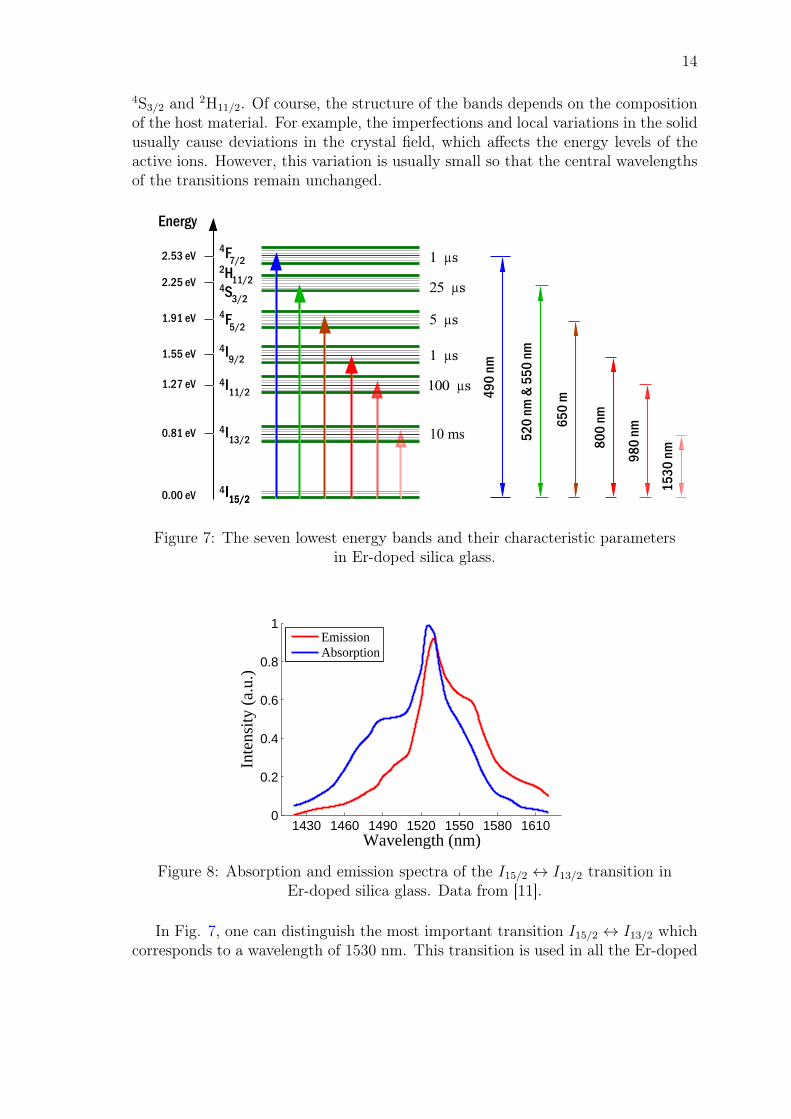
Figure 7 shows the seven lowest energy bands and their lifetimes in Er-dopedsilica glass [13]. The original energy levels in a free Er-ion are now split into energybands due to the Stark effect arising from the crystal field of the glass material.The number of energy levels generated in the specific band is given by (2J + 1)/2,where J is the total angular momentum of the state [9]. For example, the firstexcited state, I13/2, is split into 7 energy levels. The energy bands are labeled usingthe Russel-Saunders notation 2S+1LJ , where S is the total spin quantum number ofthe state, L the total orbital quantum number of the state and J the total angularmomentum ~J = ~L+ ~S of the state [34]. The 6th energy band consists of two states,
13
4f-leve
l
2)
Ato
mic int
eraction
s break th
e de
gene
racy
1) Initial situa
tion
:Th
e 4f-leve
l is 7
-tim
esde
gene
rate
d
Er-ion
Tran
sition
s forbidde
n du
e to
same
parity
of th
ewavefun
ctions
x
x
3)
Dop
ing to
solid
environm
ent: C
rystal field
causes little
to n
o pe
rturba
tion
to
the
wavefun
ctions o
f th
e initial stat
es
4)
The
crysta
l fie
ld o
f th
e solid
also
breaks t
he
sub-
energy
lev
els into
sm
all en
ergy
ban
ds d
ue
to S
tark e
ffect
Tran
sition
s allowed
be
cause
the
parity
of
the
wavefun
ctions h
as
been
broken
�
�
Figure 6: The generation of energy levels in Er3+ (blue) and Erbium-dopedhost material (green).
14
4S3/2 and 2H11/2. Of course, the structure of the bands depends on the compositionof the host material. For example, the imperfections and local variations in the solidusually cause deviations in the crystal field, which affects the energy levels of theactive ions. However, this variation is usually small so that the central wavelengthsof the transitions remain unchanged.
Energy
490
nm
520
nm &
550
nm
650
m
800
nm
980
nm
1530
nm
0.81 eV
1.27 eV
1.55 eV
1.91 eV
2.25 eV
2.53 eV
0.00 eV
1 ms
25 ms
5 ms
1 ms
100 ms
10 ms
I15/2I15/2
I13/2
I11/2
I9/2
F5/2
F7/2
S3/2
4
4
4
4
4
4H11/2
2
4
Figure 7: The seven lowest energy bands and their characteristic parametersin Er-doped silica glass.
1430 1460 1490 1520 1550 1580 16100
0.2
0.4
0.6
0.8
1
Wavelength (nm)
Inte
nsity
(a.
u.)
EmissionAbsorption
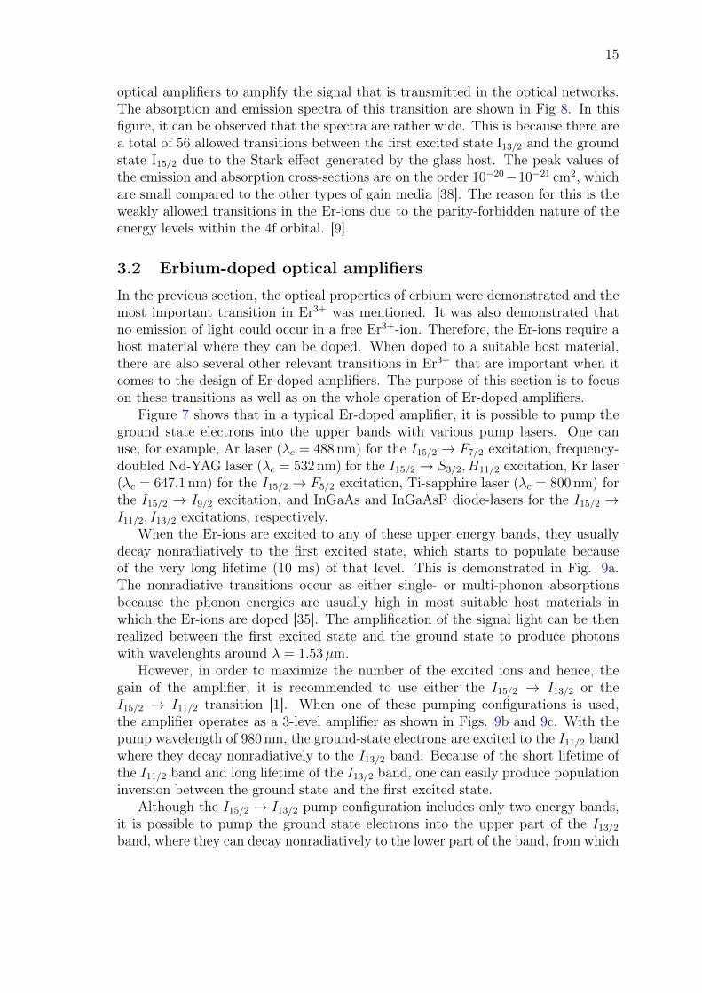
Figure 8: Absorption and emission spectra of the I15/2 ↔ I13/2 transition inEr-doped silica glass. Data from [11].
In Fig. 7, one can distinguish the most important transition I15/2 ↔ I13/2 whichcorresponds to a wavelength of 1530 nm. This transition is used in all the Er-doped
15
optical amplifiers to amplify the signal that is transmitted in the optical networks.The absorption and emission spectra of this transition are shown in Fig 8. In thisfigure, it can be observed that the spectra are rather wide. This is because there area total of 56 allowed transitions between the first excited state I13/2 and the groundstate I15/2 due to the Stark effect generated by the glass host. The peak values ofthe emission and absorption cross-sections are on the order 10−20−10−21 cm2, whichare small compared to the other types of gain media [38]. The reason for this is theweakly allowed transitions in the Er-ions due to the parity-forbidden nature of theenergy levels within the 4f orbital. [9].
3.2 Erbium-doped optical amplifiers
In the previous section, the optical properties of erbium were demonstrated and themost important transition in Er3+ was mentioned. It was also demonstrated thatno emission of light could occur in a free Er3+-ion. Therefore, the Er-ions require ahost material where they can be doped. When doped to a suitable host material,there are also several other relevant transitions in Er3+ that are important when itcomes to the design of Er-doped amplifiers. The purpose of this section is to focuson these transitions as well as on the whole operation of Er-doped amplifiers.
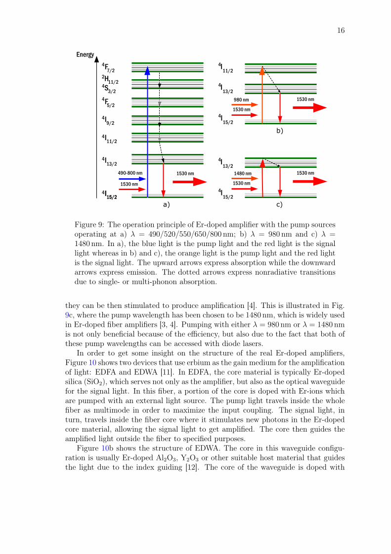
Figure 7 shows that in a typical Er-doped amplifier, it is possible to pump theground state electrons into the upper bands with various pump lasers. One canuse, for example, Ar laser (λc = 488 nm) for the I15/2 → F7/2 excitation, frequency-doubled Nd-YAG laser (λc = 532 nm) for the I15/2 → S3/2, H11/2 excitation, Kr laser(λc = 647.1 nm) for the I15/2 → F5/2 excitation, Ti-sapphire laser (λc = 800 nm) forthe I15/2 → I9/2 excitation, and InGaAs and InGaAsP diode-lasers for the I15/2 →I11/2, I13/2 excitations, respectively.
When the Er-ions are excited to any of these upper energy bands, they usuallydecay nonradiatively to the first excited state, which starts to populate becauseof the very long lifetime (10 ms) of that level. This is demonstrated in Fig. 9a.The nonradiative transitions occur as either single- or multi-phonon absorptionsbecause the phonon energies are usually high in most suitable host materials inwhich the Er-ions are doped [35]. The amplification of the signal light can be thenrealized between the first excited state and the ground state to produce photonswith wavelenghts around λ = 1.53µm.
However, in order to maximize the number of the excited ions and hence, thegain of the amplifier, it is recommended to use either the I15/2 → I13/2 or theI15/2 → I11/2 transition [1]. When one of these pumping configurations is used,the amplifier operates as a 3-level amplifier as shown in Figs. 9b and 9c. With thepump wavelength of 980 nm, the ground-state electrons are excited to the I11/2 bandwhere they decay nonradiatively to the I13/2 band. Because of the short lifetime ofthe I11/2 band and long lifetime of the I13/2 band, one can easily produce populationinversion between the ground state and the first excited state.
Although the I15/2 → I13/2 pump configuration includes only two energy bands,it is possible to pump the ground state electrons into the upper part of the I13/2
band, where they can decay nonradiatively to the lower part of the band, from which
16
Energy
1530 nm
490-800 nm 1530 nm
980 nm 1530 nm
a)
b)
1530 nm
1480 nm 1530 nm
c)
1530 nm
I15/2
I13/2
I11/2
I15/2
I13/2
I15/2I15/2
I13/2
I11/2
I9/2
F5/2
F7/2
S3/2
4
4
4
4
4
4H11/2
2
4
4
4
4
4
4
Figure 9: The operation principle of Er-doped amplifier with the pump sourcesoperating at a) λ = 490/520/550/650/800 nm; b) λ = 980 nm and c) λ =1480 nm. In a), the blue light is the pump light and the red light is the signallight whereas in b) and c), the orange light is the pump light and the red lightis the signal light. The upward arrows express absorption while the downwardarrows express emission. The dotted arrows express nonradiative transitionsdue to single- or multi-phonon absorption.
they can be then stimulated to produce amplification [4]. This is illustrated in Fig.9c, where the pump wavelength has been chosen to be 1480 nm, which is widely usedin Er-doped fiber amplifiers [3, 4]. Pumping with either λ = 980 nm or λ = 1480 nmis not only beneficial because of the efficiency, but also due to the fact that both ofthese pump wavelengths can be accessed with diode lasers.
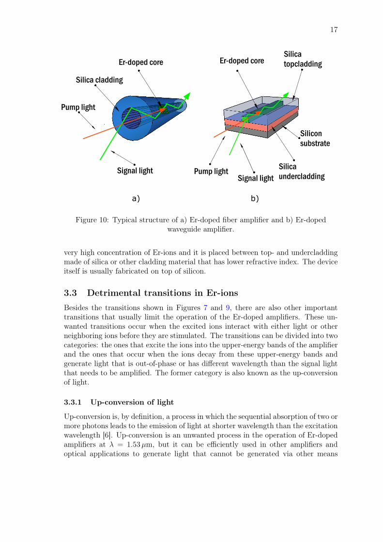
In order to get some insight on the structure of the real Er-doped amplifiers,Figure 10 shows two devices that use erbium as the gain medium for the amplificationof light: EDFA and EDWA [11]. In EDFA, the core material is typically Er-dopedsilica (SiO2), which serves not only as the amplifier, but also as the optical waveguidefor the signal light. In this fiber, a portion of the core is doped with Er-ions whichare pumped with an external light source. The pump light travels inside the wholefiber as multimode in order to maximize the input coupling. The signal light, inturn, travels inside the fiber core where it stimulates new photons in the Er-dopedcore material, allowing the signal light to get amplified. The core then guides theamplified light outside the fiber to specified purposes.
Figure 10b shows the structure of EDWA. The core in this waveguide configu-ration is usually Er-doped Al2O3, Y2O3 or other suitable host material that guidesthe light due to the index guiding [12]. The core of the waveguide is doped with
17
Silica topcladdingEr-doped core
Silicon substrate
Silica undercladding
Silica cladding
Er-doped core
Signal light
Pump light
Signal light
a) b)
Pump light
Figure 10: Typical structure of a) Er-doped fiber amplifier and b) Er-dopedwaveguide amplifier.
very high concentration of Er-ions and it is placed between top- and undercladdingmade of silica or other cladding material that has lower refractive index. The deviceitself is usually fabricated on top of silicon.
3.3 Detrimental transitions in Er-ions
Besides the transitions shown in Figures 7 and 9, there are also other importanttransitions that usually limit the operation of the Er-doped amplifiers. These un-wanted transitions occur when the excited ions interact with either light or otherneighboring ions before they are stimulated. The transitions can be divided into twocategories: the ones that excite the ions into the upper-energy bands of the amplifierand the ones that occur when the ions decay from these upper-energy bands andgenerate light that is out-of-phase or has different wavelength than the signal lightthat needs to be amplified. The former category is also known as the up-conversionof light.
3.3.1 Up-conversion of light
Up-conversion is, by definition, a process in which the sequential absorption of two ormore photons leads to the emission of light at shorter wavelength than the excitationwavelength [6]. Up-conversion is an unwanted process in the operation of Er-dopedamplifiers at λ = 1.53µm, but it can be efficiently used in other amplifiers andoptical applications to generate light that cannot be generated via other means
18
or the generation is much easier by using longer wavelength pump sources. Up-conversion has found many applications in the medical industry where the generationof light at visible wavelengths from near-infrared (NIR) light sources have been used,for example, in bioimaging [42]. Up-conversion of light can occur either as energytransfer between adjacent the Er-ions or when the excited Er-ions absorb one ormore photons before relaxing to the ground state [5]. The former of these is knownas the energy-transfer up-conversion (ETU) and the latter is known as the excitedstate absorption (ESA).
In ETU process, two nearby-lying excited ions exchange energies so that oneion gains the energy of both ions. The ion that loses its energy (donor) decays toone of the lower-levels, while the ion that gains the energy (acceptor) excites toone of the upper-energy bands. In Er3+, there are two ways for the energy-transferup-conversion process to occur [11]. These can be expressed with the followingequations:
Er3+(I13/2
)+ Er3+
(I13/2
)→ Er3+
(I11/2
)+ Er3+
(I15/2
)(2)
Er3+(I11/2
)+ Er3+
(I11/2
)→ Er3+
(I15/2
)+ Er3+
(F7/2
)(3)
In the first case (ETU1), the up-conversion occurs between two ions in the firstexcited state I13/2. The acceptor ion excites to the I11/2 state while the donor iondecays to the ground state I15/2. The outcome is the loss of two excited ions in theI13/2 state that could have been stimulated to produce amplification of light. Thus,the process leads to the reduction of gain in the amplifier [11]. In the second case(ETU2), the up-conversion occurs in the second excited state I11/2 where the ionsare pumped when using λ = 980 nm pump wavelength. In ETU2, the acceptor ionexcites to the F7/2 state while the donor ion decays to the ground state. Althoughthis process does not reduce the number of excited ions in the first excited statedirectly, it reduces the pump efficiency of the amplifier because the excited ions arelost from the I11/2 state [13].
In ESA, the ions that have already been excited to the upper-bands by the pumplight can excite again by absorbing a second pump photon in the process. In theEr-ions, ESA usually occurs with 980 nm pumping in the following way [6]:
Er3+(I15/2
)+ ~ω → Er3+
(I11/2
),
Er3+(I11/2
)+ ~ω → Er3+
(F7/2
), (4)
where ~ω is the energy of the photon produced by the 980 nm pump source. Thus,the process excites a ground state ion to the pump band I11/2, where it is excitedagain to the F7/2 band. The outcome is the loss of two photons, that is, reducedpump efficiency [6].
3.3.2 Spontaneous transitions
When the Er-ions in the amplifier are excited to the upper-energy bands via thetransitions generated by the up-conversion processes, the ions can decay radiativelyor nonradiatively to the lower-energy bands. When the energy difference between
19
the excited state of the ions and the lower-lying state is small, the transition occursnonradiatively [36]. In nonradiative transition, the energy is lost to phonons whichresults as the heating of the crystal. However, if the energy difference is sufficientlyhigh and the phonon energies of the host material low, the transition occurs ra-diatively [35]. In radiative transition, the energy is lost to spontaneously emittedphotons which have random phase and energy corresponding to the energy differencebetween the energy states of the transition. Thus, spontaneous emission (SE) leadsto a noise in the amplifier. In general, there is always spontaneous emission presentwhen the Er-ions are excited. Spontaneous emission usually occurs between unsta-ble and metastable states [9]. Thus, in the Er-ions, the destination of spontaneousemission is most likely the ground state or the first excited state. If spontaneousemission is generated between the first excited state and the ground state, the am-plifier can amplify these spontaneously emitted photons. This process is known asthe amplified spontaneous emission (ASE) and it usually reduces the gain and leadsto additional noise in the amplifier [3].
Energy
I15/2I15/2
I13/2
I11/2
I9/2
F5/2
F7/2
S3/2
490
nm
520
nm &
550
nm
650
nm
800
nm
980
nm
1530
nm
SE1 ASEETU1 ETU2 ESA
4
4
4
4
4
4H11/2
2
4
SE2 SE3
Figure 11: The detrimental processes in the operation of Er-doped ampli-fiers. The processes from left to right are: energy-transfer up-conversion(ETU), excited-state absorption (ESA), spontaneous emission (SE) and am-plified spontaneous emission (ASE).
When up-conversion of light occurs via the ETU2 and ESA processes describedin the previous subsection, the Er-ions excite to the F7/2 state. Because the F7/2
state has short lifetime and only slightly higher energy than the lower-lying energystate H11/2, the Er-ions can decay either nonradiatively or radiatively from thisstate. If the transition occurs radiatively, then the Er-ions decay either to thefirst excited state I13/2 or to the ground state I15/2. As a result, the spontaneously
20
emitted photons have wavelength of either λ = 490 nm (SE1) or λ = 720 nm (SE2),which correspond to the transitions F7/2 → I15/2 and F7/2 → I13/2, respectively.If the transition occurs nonradiatively, then the electrons decay to the lower-lyingenergy state H11/2 without emitting photons in the amplifier. However, the energydifference between this state and the lower-lying state F5/2 is now higher and thetransition from the H11/2 state occurs radiatively and most likely to the groundstate, generating light with wavelength of λ = 520 nm (SE3). This charasteristicgreen light is observed in most Er-doped gain materials that operate with the pumpwavelength of λ = 980 nm [43, 44].
Thus, multiple wavelengths that have shorter wavelength than the pump wave-length are usually generated in Er-doped amplifiers. Moreover, the probability forthese up-conversion processes increase when one increases the pump power or thedensity of the Er-ions in the gain medium [6]. The detrimental transitions discussedin this section are summarized in Figure 11.
3.4 Fabrication of Er-doped materials
In the previous section, the detrimental processes which limit the operation of the Er-doped amplifiers were discussed in detail. It turns out that some of these unwantedprocesses can be avoided or reduced by fabricating the erbium-doped gain materialproperly. Therefore, the topic of this section is to present how erbium-doped gainmaterial should be fabricated and what host materials are suitable for the Er-ionsin order to produce amplifiers with as high gain and low noise as possible.
3.4.1 Suitable host materials
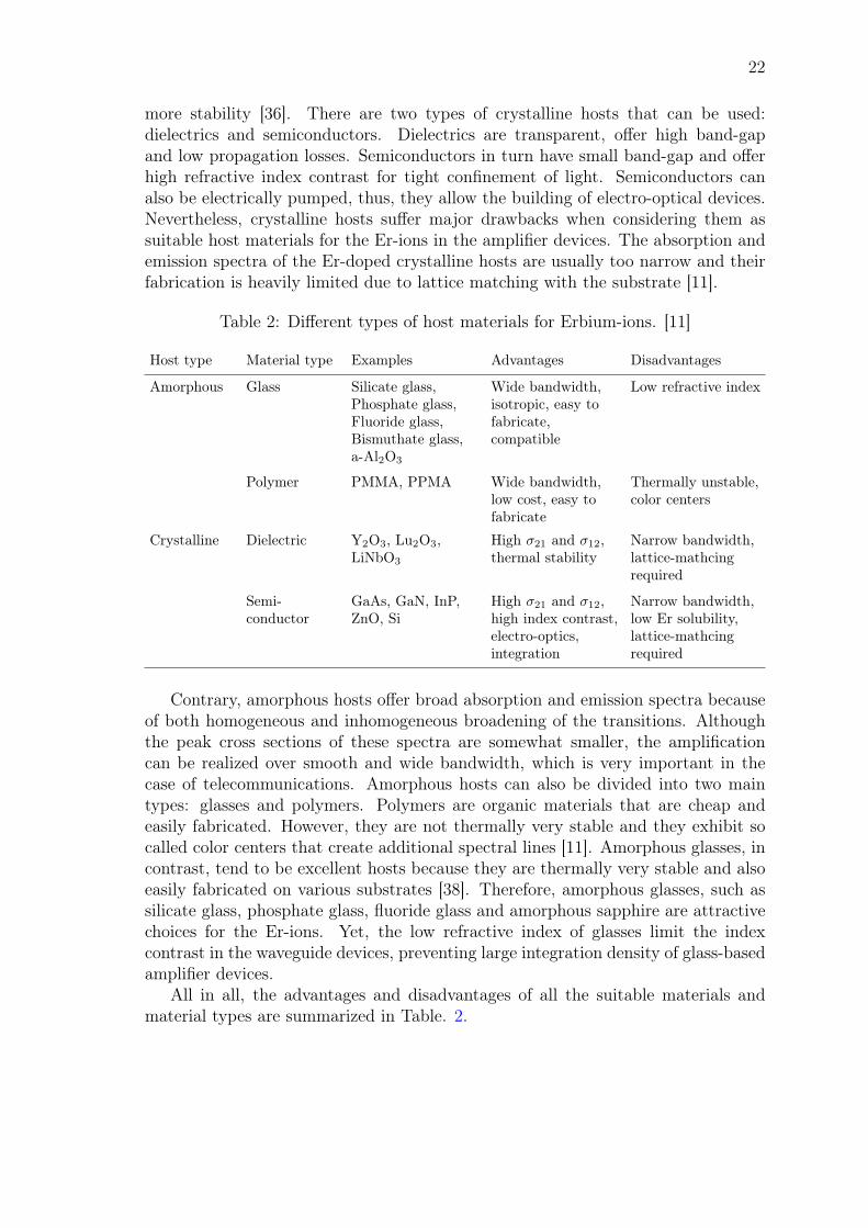
There are several requirements for the host material that need to be satisfied inorder to produce functional amplifier devices. These are listed below [11]:
1. Suitable structure for the Er-ions. The host material must posses noncentro-symmetric bonding sites for the Er-ion in order to break the parity of thewavefunctions of the energy states, allowing transitions within the 4f-shell.Furthermore, the lattice position has to be large enough to create sufficientdistance between the adjacent Er-ions. Because the oxidation state of Er3+ is+3, the ions form sesquioxides Er2O3 with oxygen. Therefore, other sesquiox-ides with approximately the same cationic radii are suitable host materials.These include, for example, Y2O3 [30], a-Al2O3 [45] and Lu2O3 [46].
2. High Er-solubility. The host material should possess the ability to be dopedwith high concentration of Er-ions without clustering. This is mandatory inshorter amplifier devices, because the gain that the amplifier can provide isproportional to
G ∝ exp [L (σ21(λ)N2(z)− σ12(λ)N1(z))] , (5)
where L is the amplifier length, N2 and N1 the number of ions in the upper-and lower-level, respectively, and σ21 and σ12 are the emission and absorp-tion cross sections, respectively [5]. From Eq. 5, one can see that the gain
21
is exponentially-dependent on the product of the device length, the numberof Er-ions in the upper- and lower-levels, and the magnitudes of the cross-sections. Because one cannot change the values of the cross-sections dramat-ically, the amount of active Er-ions should be made higher when the devicelength becomes shorter. For example, the density of the active Er-ions in atypical fiber amplifier is approximately 1017 − 1018 cm−3 so that a reasonableamplification is achieved over several meters [47]. However, when the ampli-fier is implemented in centimetre-sized devices, the density of the active ionsshould reach the orders of 1020 − 1021 cm−3 [12]. When the amount of activeions becomes this high, the ion-ion interactions start to play an important rolein the amplifier. Therefore, the active ions should not cluster inside the hostmaterial.
3. Long radiative lifetime of the I13/2 level. The host material should be able tooffer long radiative lifetime of the first excited state in order to populate theI13/2 level quickly and to produce population inversion in the amplifier.
4. Low phonon energy. The phonon energy of the amplifier is completely de-termined by the host material. The host material should have low phononenergies in order to prevent the nonradiative transitions between the first ex-cited state and the ground state.
5. High purity. As was stated in the previous chapter, the local variations andimpurities affect the absorption and emission spectrum. Therefore, the hostmaterial should have high purity in order to prevent this.
6. Chemically and physically stable. The host material should be mechanicallyhard and stable and it should also posses high thermal stability and conduc-tivity.
7. Fabrication technology. Finally, the host material should be easy enough tofabricate and doped with the current fabrication technology. Of course, thehost material should also be cheap and the technology that provides the hostmaterial should be compatible with the integrated devices that use the ampli-fier.
In general, there are two types of materials that can be used as a host for the Er-ions: crystalline and amorphous. A crystalline host consists of well-defined crystalplanes and atomic orientations whereas this kind of organized structure cannot befound in amorphous hosts. The behaviour of the Er-ions in both of these materialtypes differ greatly with respect to each other. However, both material types offertheir own advantages that depend on the application at issue.
Crystalline hosts offer very narrow absorption and emission spectra as well ashigh peak cross-sections because of the well-oriented crystal structure of the atoms.In crystalline hosts, very little to none defects and local variations can be found,leading to reduced phonon broadening and energy-band generation. Moreover, thecrystalline structure also offers high thermal conductivity for electrons which enables
22
more stability [36]. There are two types of crystalline hosts that can be used:dielectrics and semiconductors. Dielectrics are transparent, offer high band-gapand low propagation losses. Semiconductors in turn have small band-gap and offerhigh refractive index contrast for tight confinement of light. Semiconductors canalso be electrically pumped, thus, they allow the building of electro-optical devices.Nevertheless, crystalline hosts suffer major drawbacks when considering them assuitable host materials for the Er-ions in the amplifier devices. The absorption andemission spectra of the Er-doped crystalline hosts are usually too narrow and theirfabrication is heavily limited due to lattice matching with the substrate [11].
Table 2: Different types of host materials for Erbium-ions. [11]
Host type Material type Examples Advantages Disadvantages
High σ21 and σ12,high index contrast,electro-optics,integration
Narrow bandwidth,low Er solubility,lattice-mathcingrequired
Contrary, amorphous hosts offer broad absorption and emission spectra becauseof both homogeneous and inhomogeneous broadening of the transitions. Althoughthe peak cross sections of these spectra are somewhat smaller, the amplificationcan be realized over smooth and wide bandwidth, which is very important in thecase of telecommunications. Amorphous hosts can also be divided into two maintypes: glasses and polymers. Polymers are organic materials that are cheap andeasily fabricated. However, they are not thermally very stable and they exhibit socalled color centers that create additional spectral lines [11]. Amorphous glasses, incontrast, tend to be excellent hosts because they are thermally very stable and alsoeasily fabricated on various substrates [38]. Therefore, amorphous glasses, such assilicate glass, phosphate glass, fluoride glass and amorphous sapphire are attractivechoices for the Er-ions. Yet, the low refractive index of glasses limit the indexcontrast in the waveguide devices, preventing large integration density of glass-basedamplifier devices.
All in all, the advantages and disadvantages of all the suitable materials andmaterial types are summarized in Table. 2.
23
3.4.2 Fabrication techniques
There are many fabrication methods that can be used to produce Er-doped mate-rials, each with their own advantages and disadvantages. At least, the followingfabrication methods have been used to produce erbium as dopant in suitable hostmaterials: Atomic layer deposition [15], dip-coating [16], flame hydrolysis [17], high-vacuum chemical vapour deposition [18], plasma-enhanced chemical vapour depo-sition [19], pulsed laser deposition [20], reactive co-sputtering [21], RF-sputtering[22], sol-gel method [23], spin coating [24] and vapour phase deposition [25]. Someof these fabrication methods can be used to deposit the host material at the sametime as the doping of the Er-ions is done. However, the doping technique of thesemethods differ from each other somewhat radically. In most of these techniques, thedoping leads to non-uniform distribution of the Er-ions in the host material.
As was discussed previously in this chapter, the ETU-processes are importantwhen the doping concentration becomes high in the amplifier. The probabilityfor any ion-ion interaction process is proportional to 1/r6, where r is the distancebetween the neighboring ions [11]. In short devices, this brings major challengein implementing the Er-ions into the host material because the dimensions of thedevice cannot be changed. Therefore, the only way to maximize the number of theEr-ions to realize high amplification, and hence, gain, is to increase the density ofthe Er-ions. Besides the distance between adjacent ions, the probability for theETU-process to occur has also been found to depend on the homogeneity of theEr-ion profile [11]. Thus, the fabrication method must possess the ability to controlthe Er-ion profile in the host material to avoid the ion-ion interactions that lead tothe energy-transfer up-conversion in the amplifier. Besides the control of the Er-ionprofile inside the host material, it is very ideal if the fabrication technology couldoffer the production of the host material and the application to integrated devicesas well. It turns out that ALD, which has been chosen as the fabrication methodin this work can offer all of these techniques at the same time and in a single run.Therefore, ALD offers an unique way to fabricate Er-doped amplifier devices.
24
4 Atomic layer depositionALD is a chemical vapour phase deposition method that can produce thin filmswith excellent quality. It was first demonstrated by Suntola et al. as atomic layerepitaxy in 1977 in Finland [48]. Since then, ALD has gained much popularity as analternative thin film deposition technique due to its unique deposition properties,such as high conformality, aspect ratio and non-uniformity. As the semiconductorindustry has ever increasing demand for the miniaturization of components, newdeposition techniques are needed in order to coat these nanometer-sized structuresconformally with very high aspect ratio. ALD is the answer to this problem becauseno other thin film technique can approach the conformality achieved by ALD onhigh aspect structures [49].
4.1 Operation principle
The operation of ALD is based on the sequential use of a gas or vapor phase chemi-cals. As distinct from the other vapor phase techniques, in ALD, the source vaporsare pulsed into the reactor alternately, one at a time [26]. This results in a uniqueself-limiting film growth mechanism with a number of advances as discussed in Sec-tion 4.3.
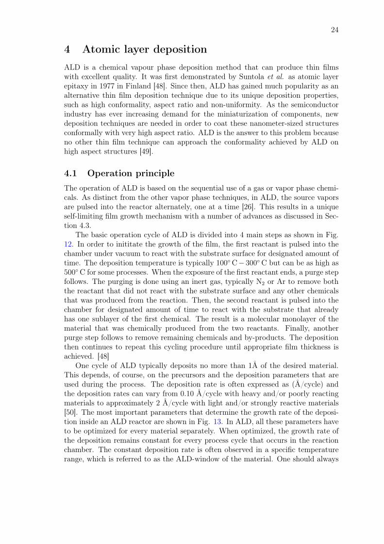
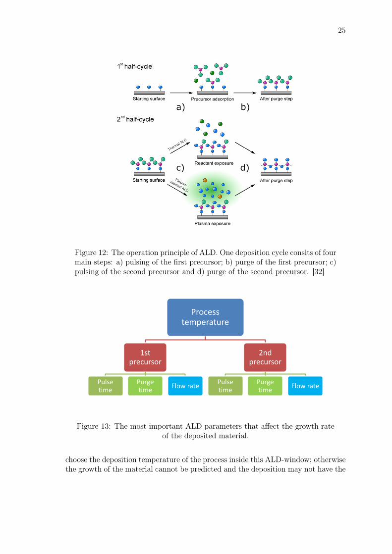
The basic operation cycle of ALD is divided into 4 main steps as shown in Fig.12. In order to inititate the growth of the film, the first reactant is pulsed into thechamber under vacuum to react with the substrate surface for designated amount oftime. The deposition temperature is typically 100◦ C− 300◦ C but can be as high as500◦ C for some processes. When the exposure of the first reactant ends, a purge stepfollows. The purging is done using an inert gas, typically N2 or Ar to remove boththe reactant that did not react with the substrate surface and any other chemicalsthat was produced from the reaction. Then, the second reactant is pulsed into thechamber for designated amount of time to react with the substrate that alreadyhas one sublayer of the first chemical. The result is a molecular monolayer of thematerial that was chemically produced from the two reactants. Finally, anotherpurge step follows to remove remaining chemicals and by-products. The depositionthen continues to repeat this cycling procedure until appropriate film thickness isachieved. [48]
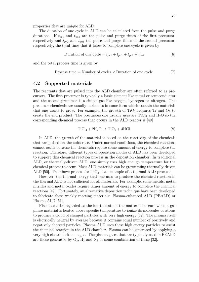
One cycle of ALD typically deposits no more than 1Å of the desired material.This depends, of course, on the precursors and the deposition parameters that areused during the process. The deposition rate is often expressed as (Å/cycle) andthe deposition rates can vary from 0.10 Å/cycle with heavy and/or poorly reactingmaterials to approximately 2 Å/cycle with light and/or strongly reactive materials[50]. The most important parameters that determine the growth rate of the deposi-tion inside an ALD reactor are shown in Fig. 13. In ALD, all these parameters haveto be optimized for every material separately. When optimized, the growth rate ofthe deposition remains constant for every process cycle that occurs in the reactionchamber. The constant deposition rate is often observed in a specific temperaturerange, which is referred to as the ALD-window of the material. One should always
25
a) b)
c) d)
Figure 12: The operation principle of ALD. One deposition cycle consits of fourmain steps: a) pulsing of the first precursor; b) purge of the first precursor; c)pulsing of the second precursor and d) purge of the second precursor. [32]
Process temperature
1st precursor
Pulse time
Purge time
Flow rate
2nd precursor
Pulse time
Purge time
Flow rate
Figure 13: The most important ALD parameters that affect the growth rateof the deposited material.
choose the deposition temperature of the process inside this ALD-window; otherwisethe growth of the material cannot be predicted and the deposition may not have the
26
properties that are unique for ALD.The duration of one cycle in ALD can be calculated from the pulse and purge
durations. If tpr1 and tpu1 are the pulse and purge times of the first precursor,respectively and tpr2 and tpu1 the pulse and purge times of the second precursor,respectively, the total time that it takes to complete one cycle is given by
Duration of one cycle = tpr1 + tpu1 + tpr2 + tpu2 (6)
and the total process time is given by
Process time = Number of cycles×Duration of one cycle. (7)
4.2 Supported materials
The reactants that are pulsed into the ALD chamber are often referred to as pre-cursors. The first precursor is typically a basic element like metal or semiconductorand the second precursor is a simple gas like oxygen, hydrogen or nitrogen. Theprecursor chemicals are usually molecules in some form which contain the materialsthat one wants to grow. For example, the growth of TiO2 requires Ti and O2 tocreate the end product. The precursors one usually uses are TiCl4 and H2O so thecorresponding chemical process that occurs in the ALD reactor is [49]
TiCl4 + 2H2O→ TiO2 + 4HCl. (8)
In ALD, the growth of the material is based on the reactivity of the chemicalsthat are pulsed on the substrate. Under normal conditions, the chemical reactionscannot occur because the chemicals require some amount of energy to complete thereaction. Therefore, different types of operation modes of ALD has been developedto support this chemical reaction process in the deposition chamber. In traditionalALD, or thermally-driven ALD, one simply uses high enough temperature for thechemical process to occur. Most ALD-materials can be grown using thermally-drivenALD [50]. The above process for TiO2 is an example of a thermal ALD process.
However, the thermal energy that one uses to produce the chemical reaction inthe thermal ALD is not sufficient for all materials. For example, some metals, metalnitrides and metal oxides require larger amount of energy to complete the chemicalreactions [49]. Fortunately, an alternative deposition technique have been developedto fabricate these weakly reacting materials: Plasma-enhanced ALD (PEALD) orPlasma ALD [51].
Plasma can be regarded as the fourth state of the matter. It occurs when a gasphase material is heated above specific temperature to ionize its molecules or atomsto produce a cloud of charged particles with very high energy [52]. The plasma itselfis electrically neutral by average because it contains equal number of positively andnegatively charged particles. Plasma ALD uses these high energy particles to assistthe chemical reaction in the ALD chamber. Plasma can be generated by applying avery high electric field on a gas. The plasma gases that are typically used in PEALDare those generated by O2, H2 and N2 or some combination of these [32].
27
PEALD has many advantages over thermal ALD. Firstly, the plasma processoffers more freedom when choosing the deposition parameters because the chemicalreaction can be easily produced. This includes the choosing of the precursors anddeposition parameters [51]. Moreover, with PEALD, it is possible to deposit single-element ALD materials, such as metals or semiconductors which were not possiblebefore the PEALD was invented [49]. For example, the fabrication of tantalium (Ta)can be produced with PEALD using hydrogen radicals as [49]
TaCl5 + 5H· → Ta + 5HCl. (9)
It has been reported that the materials deposited with the PEALD can havebetter material properties than those deposited with the thermal ALD. The materialproperties that are enhanced can be, for example, film density, impurity content orelectronic properties [32]. Moreover, the plasma processes can be conducted atreduced substrate temperatures, because the thermal energy is replaced with theenergy produced by the plasma. Furthermore, with PEALD, the growth rates areusually higher than those of thermal ALD because the plasma radicals generatehigher density of reactive surface sites at the sample. The addition of plasma also
Table 3: Supported materials with PEALD. [32]
Plasma H2 O2 N2, N2O or NH3 H2/N2 O2/N2
Material Ag, Al, Al2O3,Co, Cu,GeSbxTey,HfN, NbN, Ni,Ta, TaCxNy,TaNx, Ti,TiNx, TiAlxNy,ZrN
allows one to control the material composition because of the plasma radicals andadditional parameters that can be controlled [50]. Table 3 lists all the materials thathave been succesfully deposited with PEALD and the radical that has been used inthe process [32].
4.3 Advantages and disadvantages
ALD in general offers a variety of advantages over other thin film deposition tech-niques. Firstly, because ALD produces films monolayer by monolayer, high-qualityfilms with precise thickness, high aspect ratio and typically excellent conformalitycan be produced [53]. The layer-by-layer deposition of ALD allows the nanoscaleengineering of the deposited film, which can be used to precisely design the com-position of the ALD-grown materials. Because of this, it is also possible to growmultilayer films and nanolaminates with ALD [54]. Moreover, the growth of the ma-terial is not limited to flat surfaces: the material grows uniformly on every surface
28
of the sample that is placed in the reactor. This is a very important advantage whendepositing thin films on complicated structures; there is no need to do additionallithography steps in order to fabricate desired structures. Thus, ALD has becomevery popular technique in silicon photonics where, for example, the top cladding ofsilicon slot waveguides can be fabricated very delicately [28, 55]. Contrary to othervapor phase techniques, such as chemical or physical vapor phase deposition, themoderate deposition temperature in also allows ALD to be used with integratedcircuit structures to deposit high-k gate oxides [56].
Although ALD offers very impressive features, it also suffers from some draw-backs that limit its operation in general. Because of the layer-by-layer nature of thedeposition and the purge processes used between each precursor pulsing, the depo-sition rate of ALD is very slow compared to other techniques. Most ALD materialsrequire effective pathways for the chemical reactions to occur, thus, limiting theavailable precursors one can use [50]. Moreover, the precursors should be volatileenough to use them in gas phase at moderate temperatures [32]. Although theprocess support for materials is vast, one cannot grow some very important materi-als effectively with ALD. For example, most single-element metals, such as copperare very challenging to grow with ALD because the self-limiting growth cannot bereached easily with the precursors that are currently available for the processes [50].
4.4 Previous study on ALD-grown Er2O3
As was mentioned in Chapter 1, there are only few research groups that have stud-ied the fabrication of Er2O3 with ALD. Therefore, the concept is still very youngand requires further studies. Päiväsaari et al. have reported on the atomic-layer-deposited rare-earth oxides and their properties, especially in gate oxides. In [15],they fabricated thin Er2O3 films using tris(2,2,6,6-tetramethyl-3,5-heptanedionato)erbium (Er(thd)3) and ozone as the precursors. They found that the growth rateof Er2O3 was 0.25Å per cycle in the optimized deposition temperature window andprecursor temperature of 250 − 375 ◦C and 130 ◦C, respectively. In [56], Päiväsaariet al. deposited Er2O3 using Er(CpMe)3 and water as the precursors in their ALD.They demonstrated that the growth rate of Er2O3 could be increased dramaticallywith this process, up to 1.5 Å/cycle with the deposition temperatures of 250 ◦C and300 ◦C.
Van et al. studied the growth of Er2O3 with radical-enhanced ALD usingEr(thd)3 and O-radicals. Van et al. was able to produce Er2O3 with the growthrate of 0.3 Å/cycle at the deposition temperature of 330 ◦C [30]. Xu et al. depositedEr2O3 with ALD using Er(CpMe)3 and ozone as the precursors [29]. The growthrate of their films was 1.2 Å/cycle in the ALD temperature window of 170− 330 ◦C.
Blanquart et al. fabricated Er2O3 using three novel cyclopentadienyl precursors,Er(PrCp)3, Er(CpMe)2 and Er(BuCp)3 with either ozone or water as the precur-sors in their depositions [31]. With Er(MeCp)2, they reported the growth rates of1.2 Å/cycle and 0.4 Å/cycle with water and ozone precursors, respectively. WithEr(PrCp) precursor, Blanquart et al. reported the growth rates of 0.4 Å/cycle and1.0 Å/cycle with ozone and water, respectively. In the last part, they obtained the
29
growth rates of 0.9 Å/cycle and 1.4 Å/cycle for the Er(BuCp)3 precursor with ozoneand water, respectively.
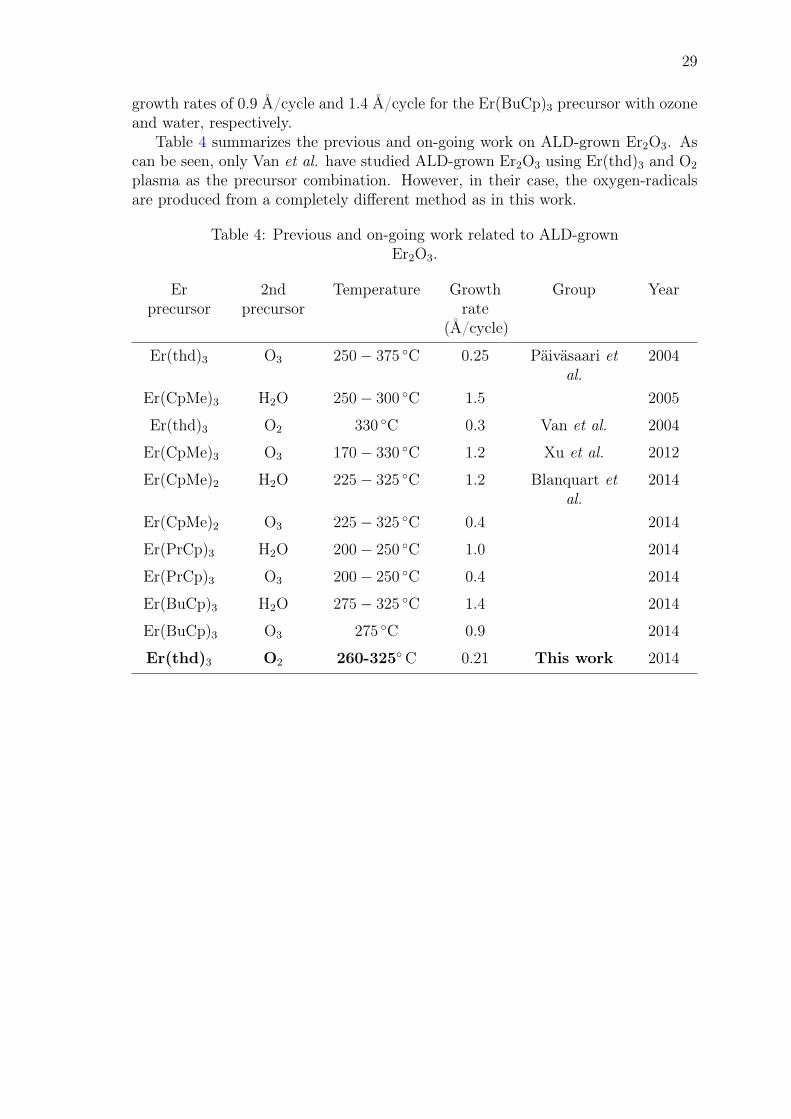
Table 4 summarizes the previous and on-going work on ALD-grown Er2O3. Ascan be seen, only Van et al. have studied ALD-grown Er2O3 using Er(thd)3 and O2
plasma as the precursor combination. However, in their case, the oxygen-radicalsare produced from a completely different method as in this work.
Table 4: Previous and on-going work related to ALD-grownEr2O3.
Erprecursor
2ndprecursor
Temperature Growthrate
(Å/cycle)
Group Year
Er(thd)3 O3 250− 375 ◦C 0.25 Päiväsaari etal.
2004
Er(CpMe)3 H2O 250− 300 ◦C 1.5 2005
Er(thd)3 O2 330 ◦C 0.3 Van et al. 2004
Er(CpMe)3 O3 170− 330 ◦C 1.2 Xu et al. 2012
Er(CpMe)2 H2O 225− 325 ◦C 1.2 Blanquart etal.
2014
Er(CpMe)2 O3 225− 325 ◦C 0.4 2014
Er(PrCp)3 H2O 200− 250 ◦C 1.0 2014
Er(PrCp)3 O3 200− 250 ◦C 0.4 2014
Er(BuCp)3 H2O 275− 325 ◦C 1.4 2014
Er(BuCp)3 O3 275 ◦C 0.9 2014
Er(thd)3 O2 260-325◦ C 0.21 This work 2014
30
5 Experimental toolsThis chapter presents the fabrication and characterization tools related to this the-sis. First, the ALD device that has been used to develop the process for Er2O3
is described. Then, the ellipsometer that is used to measure the thicknesses andrefractive indices of the as-deposited samples is presented. Finally, the the opticalsetups that are used to measure the optical properties of the samples are expressed.
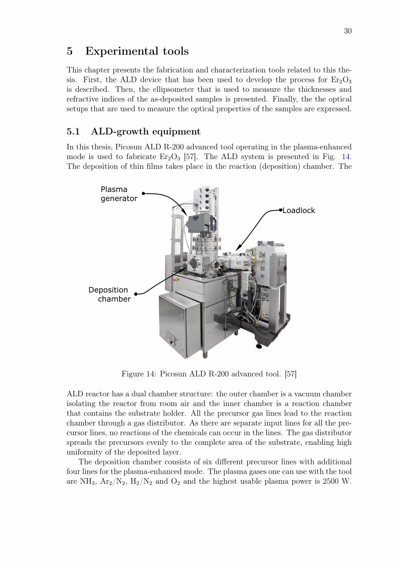
5.1 ALD-growth equipment
In this thesis, Picosun ALD R-200 advanced tool operating in the plasma-enhancedmode is used to fabricate Er2O3 [57]. The ALD system is presented in Fig. 14.The deposition of thin films takes place in the reaction (deposition) chamber. The
Loadlock
Plasmagenerator
Deposition chamber
Figure 14: Picosun ALD R-200 advanced tool. [57]
ALD reactor has a dual chamber structure: the outer chamber is a vacuum chamberisolating the reactor from room air and the inner chamber is a reaction chamberthat contains the substrate holder. All the precursor gas lines lead to the reactionchamber through a gas distributor. As there are separate input lines for all the pre-cursor lines, no reactions of the chemicals can occur in the lines. The gas distributorspreads the precursors evenly to the complete area of the substrate, enabling highuniformity of the deposited layer.
The deposition chamber consists of six different precursor lines with additionalfour lines for the plasma-enhanced mode. The plasma gases one can use with the toolare NH3, Ar2/N2, H2/N2 and O2 and the highest usable plasma power is 2500 W.
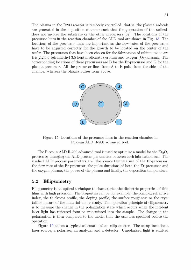
31
The plasma in the R200 reactor is remotely controlled, that is, the plasma radicalsare generated in the deposition chamber such that the generation of the radicalsdoes not involve the substrate or the other precursors [32]. The locations of theprecursor lines in the reaction chamber of the ALD tool are shown in Fig. 15. Thelocations of the precursor lines are important as the flow rates of the precursorshave to be adjusted correctly for the growth to be located on the center of thewafer. The precursors that have been chosen for the fabrication of erbium oxide aretris(2,2,6,6-tetramethyl-3,5-heptanedionato) erbium and oxygen (O2) plasma. Thecorresponding locations of these precursors are B for the Er-precursor and G for theplasma-precursor. All the precursor lines from A to E pulse from the sides of thechamber whereas the plasma pulses from above.
C B
FE
D G A
Figure 15: Locations of the precursor lines in the reaction chamber inPicosun ALD R-200 advanced tool.
The Picosun ALD R-200 advanced tool is used to optimize a model for the Er2O3
process by changing the ALD process parameters between each fabrication run. Thestudied ALD process parameters are: the source temperature of the Er-precursor,the flow rate of the Er-precursor, the pulse durations of both the Er-precursor andthe oxygen plasma, the power of the plasma and finally, the deposition temperature.
5.2 Ellipsometry
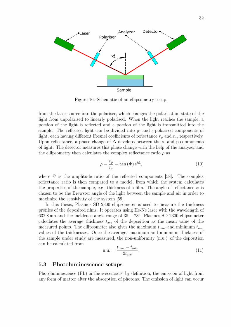
Ellipsometry is an optical technique to characterize the dielectric properties of thinfilms with high precision. The properties can be, for example, the complex refractiveindex, the thickness profile, the doping profile, the surface roughness or the crys-talline nature of the material under study. The operation principle of ellipsometryis to measure the change in the polarization state which occurs when the incidentlaser light has reflected from or transmitted into the sample. The change in thepolarization is then compared to the model that the user has specified before theoperation.
Figure 16 shows a typical schematic of an ellipsometer. The setup includes alaser source, a polariser, an analyzer and a detector. Unpolarised light is emitted
32
LaserPolariser
Analyzer Detector
Sample
y
Figure 16: Schematic of an ellipsometry setup.
from the laser source into the polariser, which changes the polarisation state of thelight from unpolarised to linearly polarised. When the light reaches the sample, aportion of the light is reflected and a portion of the light is transmitted into thesample. The reflected light can be divided into p- and s-polarised components oflight, each having different Fresnel coefficients of reflectance rp and rs, respectively.Upon reflectance, a phase change of ∆ develops between the s- and p-componentsof light. The detector measures this phase change with the help of the analyzer andthe ellipsometry then calculates the complex reflectance ratio ρ as
ρ =rprs
= tan (Ψ) ei∆, (10)
where Ψ is the amplitude ratio of the reflected components [58]. The complexreflectance ratio is then compared to a model, from which the system calculatesthe properties of the sample, e.g. thickness of a film. The angle of reflectance ψ ischosen to be the Brewster angle of the light between the sample and air in order tomaximize the sensitivity of the system [59].
In this thesis, Plasmos SD 2300 ellipsometer is used to measure the thicknessprofiles of the deposited films. It operates using He-Ne laser with the wavelength of632.8 nm and the incidence angle range of 35− 73◦. Plasmos SD 2300 ellipsometercalculates the average thickness tave of the deposition as the mean value of themeasured points. The ellipsometer also gives the maximum tmax and minimum tmin
values of the thicknesses. Once the average, maximum and minimum thickness ofthe sample under study are measured, the non-uniformity (n.u.) of the depositioncan be calculated from
n.u. =tmax − tmin
2tave
. (11)
5.3 Photoluminescence setups
Photoluminescence (PL) or fluorescence is, by definition, the emission of light fromany form of matter after the absorption of photons. The emission of light can occur
33
immediately after the excitation or after several nonradiative transition processes.The time between the absorption and emission of photons vary from femtosecondsto milliseconds, depending on the material under study [53]. PL can be used toinvestigate the excited state energies, their lifetimes or the emission spectrum ofthe material. It is often used to determine the bandgap energy of direct bandgapsemiconductors [58].
In this thesis, two optical configurations are used to study the PL of the samples.At visible wavelengths, PL is studied using Quantamaster 40 (QM40) fluorescencespectrofluorometer [60]. The schematic of this setup is presented in Fig. 17. QM40 is
Figure 17: Schematic of the Quantamaster 40 fluorescence spectrofluorometerused in this work. The components and units in the setup are: 1: High inten-sity continuous Xe lamp, 2: Adjustable slits, 3: Excitation monochromator,4: Excitation grating, 5: Sample compartment, 6: Excitation correction, 7:Emission monochromator, 8: Emission grating and 9: Detector. The sampleto be studied is placed in the middle of the sample compartment. [60]
a very optimized system for the measurements of individual photons from fluorescentsamples. Its signal-to-noise ratio is 10000:1 and detection limit of 460 attomolar offluorescein solution can be reached. QM40 uses high intensity continuous Xe lampas the excitation light source and the system contains several monochromators andgratings to separate the specific excitation and emission wavelengths of light.
QM40 can be used to measure both absorption and emission spectra of samples.However, the absorption measurement is done by measuring emission that resultsfrom the absorption process. Therefore, the system can only be used to study thelocations of the absorption bands rather than the exact absorption of the materialunder study. This is because the emission at specific wavelength cannot be relatedto the absorption at another wavelength entirely.
QM40 has both excitation and emission corrections as all light sources emitlight that is not of equal intensity across the output spectrum, which can lead toerrors in the measurement of both excitation and emission spectrum. During an
34
experiment, part of the excitation beam is diverted into a reference diode detectorprior reaching the sample. The excitation detector performs excitation correctionin real time and provides the user a corrected output that is independent of theexcitation source characteristics or any temporal fluctuation of the lamp intensity,thus ensuring excellent stability of the signal [61]. A similar phenomenon exists foremission data. The detector in the QM40 setup can be used to measure light atwavelength regime λ = 185− 820 nm.
In this thesis, QM40 spectrometer is used to measure both the absorption andemission spectra of the samples at visible and near-infrared wavelengths. The emis-sion measurements are divided into two sections. In the first section, two excitationwavelengths, λexc = 480 nm and λexc = 532 nm are chosen to measure the PL prop-erties of the samples. In the second section, two different wavelengths λexc = 800 nmand λexc = 980 nm are chosen to study the up-conversion properties of the samples.
As the QM40 fluorescence spectrometer cannot be used to measure the PL atnear-infrared (NIR) wavelengths, a separate PL-setup is used for this purpose. Fig-ure 18 shows this experimental setup. Frequency-doubled Nd:YAG laser (Verdi,
Chopper
Laser
Lenses
DetectorMonochromator
LI-amplifierComputer
ErbiumSample
F7/2S3/2F5/2I9/2I11/2I13/2
I15/2
Figure 18: Schematic of the PL-setup used in this thesis to study the PL atNIR wavelengths.
Coherent inc.) is used as the excitation source to produce light with the wavelengthof λ = 532 nm. Continuous wave operation is used and the power levels from 1 Wto 1.5 W are selected. The laser light is transmitted through a chopper operatingat frequency f = 330 Hz and then directed onto the sample with very wide angle(> 150◦). The sample is then excited and the radiation it emits is gathered with alens. The emitted light is then directed into a monochromator, which passes onlyone wavelength component at a time to the detector. The voltage of the detectoris measured as a function of the wavelength with a lock-in (LI) amplifier in orderto increase the sensitivity of the system. The lock-in amplifier is connected to acomputer which gives the data of the signal measured by the system.
In Er2O3, the pump wavelength of λ = 532 nm excites the ground state electronsinto the H11/2 band, where they can decay either radiatively or nonradiatively to anyof the lower-lying energy bands F5/2, I9/2, I11/2, I13/2 or I15/2. When the electronsdecay to these lower-lying bands, they can again, decay radiatively or nonradiatively
35
to the lower bands. In this way, the possible PL-signals that can be observed arethe wavelengths around the central wavelengths of the corresponding energy levelsin the Er-ions, that is, 650 nm, 800 nm, 980 nm and 1530 nm or the ones generatedvia transitions to lower-lying energy bands other than ground state. However, thereare also detrimental transitions present in the Er-ions as was discussed in Section3.3.
36
6 ALD process development for Er2O3
In this chapter, the atomic-layer-deposited Er2O3 process development is presentedthoroughly. The initial parameters for the first run were chosen based on the valuesPäiväsaari et al. used in [15]. Each run was performed on 6" p-type Si(100) waferusing a total of 1000 process cycles. After each process, the point-by-point thicknesswas measured with the ellipsometer and the average thickness and non-uniformityof the wafer were calculated from these values. The wafers were measured from 13different points as shown in Fig. 19. The process development is divided into 5subsections. In each subsection, the dependency of the ALD process parameters onthe thickness and the non-uniformity of Er2O3 is studied one ALD parameter at atime. The influence of the erbium source temperature is studied first.
1 3 52 4
6
7
8
9
10 11
1213
Figure 19: Locations of the measurement points for each wafer in theellipsometer.
6.1 Erbium source temperature
The ALD parameters that were used in the first Er2O3 run are shown in Table 5.The first run was performed using the erbium source temperature of 140◦ C. With
Table 5: The ALD process parameters of the first Er2O3 run.
Dep./SourceTemp.
Er(thd)3 pulse/ purge time
O2 pulse /purge time
Er(thd)3
flow rateO2 flowrate
Plasmapower/time
325/140◦ C 2.5/6.0 s 13.0/2.0 s 150 sccm 150 sccm 2500 W/10 s
the initial values shown in Table 5, the average thickness and the non-uniformityof the first deposition was measured to be 136.85 Å and 38.18 %, respectively.The average thickness of 136.85 Å with 1000 cycles yields the deposition rate ofapproximately 0.137 Å/cycle, thus, it is likely that these results are far from what
37
could be expected from the process after optimization. After the first run, thetemperature of the Er-precursor was increased in order to increase the growth rateand to decrease the non-uniformity of the deposition. The Er(thd)3 solid precursorrequires high enough temperature to produce a specific amount of vapor pressurefor the chemical to reach out of the source bottle. The temperature of the sourcewas first increased to 145◦ C and then to 150◦ C. The growth rate and the non-uniformity as a function of the temperature are shown in Fig. 20. In this figure, it
140 142 144 146 148 150
0.14
0.15
0.16
0.17
0.18
Gro
wth
rat
e (Å
/cyc
le)
Erbium source temperature (C)140 142 144 146 148 150
5
10
15
20
25
30
35
40
Non
−U
nifo
rmity
(%
)
Erbium source temperature (C)
b)a)
Figure 20: Er(thd)3 source temperature vs. a) Er2O3 growth rate and b) Er2O3
non-uniformity. The unit of the x-axis is ◦C. The other growth parametersare: Deposition temperature: 325 ◦C, Er(thd)3 flow rate: 150 sccm, Er(thd)3
pulse/purge time: 2.5/6.0 s and O2-plasma generation time/power: 10.0 s/2500W.
is observed that the temperature of 140◦ C is indeed too low and yields poor growthrate and non-uniformity, whereas 150◦ C is high enough to reach the saturation ofboth the growth rate and the non-uniformity. However, Päiväsaari et al. showedthat the Er(thd)3-precursor starts to decompose around 150◦ C. Therefore, in orderto ensure the best possible composition of the erbium chemical inside the reactor,145◦ C was chosen as the temperature for the Er-precursor for the later runs.
6.2 Erbium precursor flow rate
To study the influence of the Er-precursor flow rate on the thickness and the non-uniformity of Er2O3, four runs were performed by using four different values for theflow rate: 150 sccm, 130 sccm, 110 sccm and 100 sccm. The thickness profiles ofthe process runs were studied in order to see where the growth of each depositionwas located on the wafer. The first run in this series was performed using the sameinitial values as in the previous run, except that the erbium source temperature wasincreased to 145◦ C. The thickness profile of the first run is shown in Fig. 21. In Fig.21, one can see that most of the growth is centered on the left side of the wafer. Thisindicates that the flow rate of either precursor is too low or too high. By examining
38
Y (
cm)
X (cm)−6 −4 −2 0 2 4 6
−6
−4
−2
0
2
4
6
80
100
120
140
160
180
Figure 21: Er2O3 thickness profile when the Er(thd)3 flow rate is set to 150sccm. The unit of the color bar is Å. The other growth parameters are: de-position temperature: 325 ◦C, Er(thd)3 source temperature: 145 ◦C, Er(thd)3
pulse/purge time: 2.5/6.0 s and O2-plasma generation time/power: 10.0 s/2500W.
the locations of the precursor lines inside the deposition chamber of the PicosunALD tool, it was observed that the Er-precursor is located on the north-east side ofthe chamber during the deposition. Thus, the flow rate of the Er-precursor must betoo high. After the first run, the Er-precursor flow rate was decreased from 150 sccmto 130 sccm. The average thickness of 185.79 Å, which corresponds to the growthrate of 0.186 Å/cycle was observed and the non-uniformity remained approximatelyat the same value. The resulting thickness profile is shown in Fig. 22. By observingthe thickness profile, one can clearly see that the center of the growth has slightlymoved towards right of the wafer. Moreover, the vertical thickness of the depositionappears to be more uniform as compared to Fig. 21. Nevertheless, most of thegrowth still occurs on the left side of the wafer, thus, the flow rate requires moreoptimization.
In the third process run, the flow rate was decreased from 130 sccm to 110 sccm.The average thickness, the growth rate and the non-uniformity of the deposition wasfound to be 206.16 Å, 0.206 Å/cycle and 4.84 %, respectively. The thickness profileis shown in Fig. 23. As can be seen, the growth has shifted towards right and is nowalmost located at the center of the wafer. Motivated by this, a last process run forthe Er-precursor flow rate was performed by reducing the flow rate from 110 sccmto 100 sccm. The average thickness, the growth rate and the non-uniformity of thedeposition were found to be 209.26 Å, 0.209 Å/cycle and 4.12 %, respectively. Thethickness profile is shown in Fig. 24. The thickness profile is now almost located atthe center of the wafer and the uniformity appears to be excellent. As a result ofthe Er-precursor flow rate optimization, the growth was shifted to the center of the
39
X (cm)
Y (
cm)
−6 −4 −2 0 2 4 6
−6
−4
−2
0
2
4
6
140
150
160
170
180
190
200
Figure 22: Er2O3 thickness profile when the Er(thd)3 flow rate is set to 130sccm. The unit of the color bar is Å. The other growth parameters are: de-position temperature: 325 ◦C, Er(thd)3 source temperature: 145 ◦C, Er(thd)3
pulse/purge time: 2.5/6.0 s and O2-plasma generation time/power: 10.0 s/2500W.
X (cm)
Y (
cm)
−6 −4 −2 0 2 4 6
−6
−4
−2
0
2
4
6
195
200
205
210
Figure 23: Er2O3 thickness profile when the Er(thd)3 flow rate is set to 110sccm. The unit of the color bar is Å. The other growth parameters are: de-position temperature: 325 ◦C, Er(thd)3 source temperature: 145 ◦C, Er(thd)3
pulse/purge time: 2.5/6.0 s and O2-plasma generation time/power: 10.0 s/2500W.
wafer and at the same time, the growth rate was increased above 0.20 Å/cycle andthe non-uniformity was decreased to approximately 4 %.
40
Y (
cm)
X (cm)−6 −4 −2 0 2 4 6
−6
−4
−2
0
2
4
6
195
200
205
210
215
Figure 24: Er2O3 thickness profile when the Er(thd)3 flow rate is set to 100sccm. The unit of the color bar is Å. The other growth parameters are: de-position temperature: 325 ◦C, Er(thd)3 source temperature: 145 ◦C, Er(thd)3
pulse/purge time: 2.5/6.0 s and O2-plasma generation time/power: 10.0 s/2500W.
100 120 140
0.17
0.18
0.19
0.2
0.21
Erbium precursor flow rate (sccm)
Gro
wth
rat
e (Å
/cyc
le)
100 120 1404
6
8
10
12
14
16
Non
−un
iform
ity (
%)
Erbium precursor flow rate (sccm)
a) b)
Figure 25: Er(thd)3 flow rate vs. a) Er2O3 growth rate and b) Er2O3 non-uniformity. The other growth parameters are: deposition temperature: 325 ◦C,Er(thd)3 source temperature: 145 ◦C, Er(thd)3 pulse/purge time: 2.5/6.0 s andO2-plasma generation time and power: 10.0 s/2500 W.
To summarize, the average thickness and the non-uniformity as a function of theEr(thd)3 flow rate are shown in Fig. 25. It appears that both the non-uniformityand the growth rate have reached their saturation value. Thus, there was no needfor further optimization and the process development was proceeded to optimize thepulse times of the precursors.
41
6.3 Precursor pulse times
The growth rate and the non-uniformity of the deposited Er2O3 was studied as afunction of the precursor pulse times. First, the influence of the Er-precursor pulseduration was investigated. Five pulsing times were chosen: 1.0 s, 1.5 s, 2.0 s, 2.5 sand 3.0 s. Besides the Er-precursor pulse times, the other ALD process parametersthat were used in the optimization process are shown in Table. 6. The growth rate
Table 6: The ALD process parameters for the optimization of theEr(thd)3 pulse time. X varies from 1.0 s to 3.0 s.
Dep./SourceTemp.
Er pulse /purge time
O2 pulse /purge time
Er flowrate
O2 flowrate
Plasmapower/time
325/145◦ C X/6.0 s 13.0/2.0 s 100 sccm 150 sccm 2500 W/10.0 s
1 1.5 2 2.5 3
4
4.5
5
5.5
6
6.5
7
Erbium pulse time (s)
Non
−un
iform
ity (
%)
1 1.5 2 2.5 3
0.2
0.202
0.204
0.206
0.208
0.21
Erbium pulse time (s)
Gro
wth
rat
e (Å
/cyc
le) a) b)
Figure 26: Er(thd)3 pulse time vs. a) Er2O3 growth rate and b) Er2O3 non-uniformity. The other growth parameters are: deposition temperature: 325 ◦C,Er(thd)3 source temperature: 145 ◦C, Er(thd)3 flow rate: 100 sccm, Er(thd)3
purge time: 6.0 s and O2-plasma generation time and power: 10.0 s/2500 W.
vs. Er(thd)3 pulse time is shown in Fig. 26a and the non-uniformity vs. Er(thd)3
pulse time is shown in Fig. 26b. Again, it appears that both the non-uniformity aswell as the growth have reached their saturation value. Therefore, pulse duration of3.0 s was chosen as the best value.
After the Er-precursor pulse time optimization, the dependency of the O2-plasmaexposure time on the thickness and the non-uniformity of the process was studied.Again, five exposure times were chosen: 5.0 s, 8.0 s, 10.0 s, 15.0 s and 20.0 s. TheEr-precursor pulse time was set to 2.5 s. The growth rate vs. O2-plasma exposuretime is shown in Fig. 27a whereas the non-uniformity vs. O2-plasma exposure timeis shown in Fig. 27b. In Fig. 27, it can be observed that the saturation of the non-uniformity can be reached with 20.0 s exposure time while the growth rate could be
42
5 10 15 20
0.2
0.21
0.22
0.23
0.24
Plasma exposure time (s)
Gro
wth
rat
e (Å
/cyc
le)
5 10 15 20
4.5
5
5.5
Plasma exposure time (s)
Non
−un
iform
ity (
%)a) b)
Figure 27: O2-plasma exposure time vs. a) Er2O3 growth rate and b) Er2O3
non-uniformity. The other growth parameters are: deposition temperature:325 ◦C, Er(thd)3 source temperature: 145 ◦C, Er(thd)3 flow rate: 100 sccm,Er(thd)3 pulse/purge time: 2.5/6.0 s and O2-plasma generation power: 2500W.
made higher by increasing the plasma exposure time even further. Nevertheless, thegrowth rate was increased from approximately 0.21 Å/cycle to approximately 0.24Å/cycle by increasing the plasma exposure time from 10.0 s to 20.0 s.
However, the tradeoff with higher growth rate is the dramatic increase in theprocess duration. For example, 1000 cycles of Er2O3 with plasma exposure time of10.0 s takes approximately 6.5 hours whereas it takes 9.3 hours with 20.0 s exposuretime. Thus, there is no need to use high duration plasma pulses because the sameamount of film thickness could be produced by adding few more cycles to the process.Although this increases the consumption of the Er-precursor slightly, it saves timemore than 2 hours per run. Therefore, exposure time of 10.0 s is chosen as acompromise because the process runs would be too long with the longer exposuretimes.
6.4 Plasma power
After the precursor pulse times were optimized, the dependency of the plasma gen-eration power was studied. Three plasma generation power values were chosen: 1500W, 2000 W, and 2500 W. 2500 W was the maximum power that could be utilizedwith the plasma generator of the ALD tool. The growth rate and the non-uniformityas a function of the plasma power are shown in Fig. 28. As can be observed in Fig.28a., the growth rate reaches its saturation value at approximately 2000 W. However,the non-uniformity can still be lowered by increasing the plasma power, as can beseen in Fig. 28b. Because 2500 W is the highest value that can be used, it is chosenas the best value due to the highest growth rate and the lowest non-uniformity.
43
1500 2000 25003
3.5
4
4.5
5
5.5
6x 10
−3
Non
−un
iform
ity (
%)
Plasma power (W)1500 2000 2500
0.185
0.19
0.195
0.2
0.205
Gro
wth
rat
e (Å
/cyc
le)
Plasma power (W)
b)a)
Figure 28: O2-plasma generation power vs. a) Er2O3 growth rate and b) Er2O3
non-uniformity. The other growth parameters are: deposition temperature:325 ◦C, Er(thd)3 source temperature: 145 ◦C, Er(thd)3 flow rate: 100 sccm,Er(thd)3 pulse/purge time: 2.5/6.0 s and O2-plasma generation time: 10.0 s.
6.5 Deposition temperature
Once the Er-precursor temperature, flow rate and pulse time as well as the O2-plasmaexposure time and generation power were optimized, the deposition temperaturewas studied last. The deposition temperature was varied between 250◦ C and 325◦ Cand the growth rate of Er2O3 was studied for each temperature. Fig. 29 shows the
240 260 280 300 3200.17
0.18
0.19
0.2
0.21
0.22
Deposition temperature (C)
Gro
wth
rat
e (Å
/cyc
le)
Figure 29: Deposition temperature vs. Er2O3 growth rate. The unit of thex-axis is ◦C. The other growth parameters are: Er(thd)3 source temperature:145 ◦C, Er(thd)3 flow rate: 100 sccm, Er(thd)3 pulse/purge time: 2.5/6.0 s andO2-plasma generation time/power: 10.0 s/2500 W.
results. In this figure, a constant growth rate is obtained when the temperaturereaches 260◦ C and the growth rate stays constant up to the deposition temperature
44
of 325◦ C. Thus, the ALD-window of the process is 250◦ C − 325◦ C. It is possiblethat this window extends to even higher temperatures, as was the case in the studyby Päiväsaari et al. [15].
6.6 The optimized process
When the process optimization was completed, the process was tested by setting allthe ALD-parameters to their optimal values. Figure 30 shows the Er2O3 thicknessprofile of this deposition. The growth rate and non-uniformity of this deposition
X (cm)
Y (
cm)
−5 0 5
−6
−4
−2
0
2
4
6
208
210
212
214
216
218
220
Figure 30: Er2O3 thickness profile after the optimization of the process. Averagethickness: 214.53 Å and non-uniformity: 3.55%. The unit of the color bar isÅ. The process parameters that were used in the deposition are shown in Table11.
was calculated to be 0.215 Å/cycle and 3.55 %, respectively. The optimized ALD-parameters are listed in Table 11.
Table 7: The ALD parameters of the optimized Er2O3 process.
Dep./SourceTemp.
Er pulse /purge time
O2 pulse /purge time
Er flowrate
O2 flowrate
Plasmapower/time
325/145◦ C 3.0/6.0 s 13.0/2.0 s 100 sccm ∼ 150 sccm 2500 W/10.0 s
In order to verify that the process development was successful, the depositionrate of the optimized process should remain constant after each cycle. This wasstudied by performing three more process runs: one with 250 cycles, second with500 cycles and third with 750 cycles. If the deposition rate remains constant aftereach cycle, it indicates that the thickness of the film is a linear function of thenumber of cycles. The film thickness as a function of the number of process cycles is
45
400 600 800 1000
60
80
100
120
140
160
180
200
Film
Thi
ckne
ss (
Å)
Number of Cycles
0.20 Å/cycle
Figure 31: Number of process cycles vs. Er2O3 film thickness afteroptimization. The deposition rate is constant.
shown in Fig. 31 As can be seen, the film thickness follows the linear relation withthe amount of cycles performed. The slope of the plot gives the deposition rate,which has been calculated to be approximately 0.20 Å/cycle.
In conclusion, this chapter provided a well-working ALD-process for the fabrica-tion of Er2O3 using Er(thd)3 and O2-plasma as the precursors of the deposition. Tomy knowledge, this is the second time Er2O3 has been fabricated using ALD withO2-plasma as the oxygen source. However, the generation of the oxygen radicalsthat react with the Er-precursor is completely different than the study provided byVan et al., who used radically-enhanced ALD in their work. In the case of Van etal. the O-radicals (O, O∗, O+, O−, O2, O+
2 and O∗2) are generated before reaching
the deposition chamber, whereas in this work, the O-radicals are generated in thedeposition chamber during the process. In their case, the generation of the radicalstakes up to 10 minutes, whereas in this work, the generation time is only 10 seconds.Moreover, Van et al. only studied the surface kinetics of the reaction and did notprovide any ALD-related information on their process. Therefore, Table 4 can befilled with new information related to the deposition of Er2O3 with ALD: the com-bination of Er(thd)3 and O2-plasma yields a constant growth rate of 0.21 Å/cyclein a temperature window of 260-325◦ C.
The growth rate and the deposition temperature are somewhat in a good agree-ment with Päiväsaari et al. whose deposition of Er2O3 yielded the growth rate of0.25 Å/cycle in the temperature range of 250-375◦ C with the same Er-precursor butwith ozone as the oxygen source [15]. The reason for the lower growth rate obtainedin this work is most likely caused by the difference in the oxygen source as erbiumrequires O3 to complete the reaction into Er2O3. In this work, the O3 is provided bythe plasma reaction of O2 into O3, thus, complicating the chemical reaction slightly.However, it is also possible that the difference is caused by the use of completelydistinctive ALD-reactor in this work. Although it was shown that a deposition rateof 0.24 Å/cycle was reached with high plasma exposure time, the refractive index
46
of Er2O3 provided by this process cannot be referred to the literature value ≈ 1.9[62]. As Päiväsaari et al. did not provide the refractive index of their Er2O3 films,it is impossible to confirm what causes the difference in the growth rates betweenthis and their work.
The purge time or the flow rate of the O2-plasma precursor were not studiedin this process development, because the influence of the plasma purge time doesnot give any new information related to the process and the flow rate of the plasmacannot be controlled with the process software.
47
7 Optical characterization of Er2O3
Once the fabrication process was optimized for Er2O3, two more samples were fab-ricated in order to study the optical behaviour of Er-ions in different environments.The first sample was fabricated in the following way: the number of Er2O3 cycleswas kept constant but in addition, 2 cycles of Al2O3 were added between each Er2O3
cycle. The second sample was fabricated in the same way but with 3 cycles of Al2O3
between each Er2O3 cycle. The fabrication process is shown in Fig. 32. By addingx amounts of Al2O3-layers between each Er2O3 layer, the Er-ions are doped to theAl2O3 and the average distance between the Er3+-ions becomes larger in the verticaldirection. Al2O3 has been chosen as the host material for the Er-ions because of itsexcellent properties as a host material, as was discussed in Section 3.4. The atomic-layer-deposited Al2O3 assumes an amorphous form. The deposition parameters forAl2O3 are shown in Table 8.
Table 8: the ALD parameters of the Al2O3 process.
Dep.Temp.
TMA pulse /purge time
O2 pulse /purge time
TMAflow rate
O2 flowrate
Plasmapower/time
325◦ C 0.2/5.0 s 13.0/2.0 s 140 sccm 150 sccm 2500 W/10.0 s
Once the samples were fabricated, their average thicknesses and refractive in-dices were measured with ellipsometer. Each sample was given its own name forclarity. The names and the measured parameters are shown in Table 9. After
Er O2 3
Al O2 3x cycles
1 cycle
1000cycles
Figure 32: Fabrication process of the Er2O3-Al2O3 nanolaminates.
the fabrication, the absorption and emission spectra of the samples were studiedusing the QM40 fluorescence spectrometer and the PL setup that were presentedin Chapter 5. QM40 was used to measure the absorption and emission spectra atwavelength range 480 − 900 nm, whereas the PL-setup was used to measure PL atnear infra-red wavelengths (> 900 nm).
48
Table 9: The experimentals details of each sample.
In order to be able to study the PL of the samples, it is mandatory to know wherethe energy bands of the samples are located. The locations of the energy bandswere studied by measuring the absorption spectrum of each sample. As was notedin Section 5.3, the principle of the absorption measurement with QM40 is to mea-sure the emission that results from the absorption process. Therefore, no absolutevalues for the absorption of the samples can be given with this method. Moreover,the relative strengths of the absorption peaks in the absorption spectra cannot becompared between the samples. However, the method is still reliable to study thelocations of the energy bands in the samples.
The absorption measurements were done as follows: First, the absorption wasstudied in the wavelength range 460− 620 nm by measuring the emission at λem =800 nm. After this, the absorption was studied in the wavelength range 780−900 nmby measuring the emission at λem = 532 nm. Finally, the absorption was studied inthe wavelength range 900−1000 nm by measuring the emission at λem = 650 nm. Fig.33 presents the results from these measurements. In this figure, one can distinguishmost of the transitions that are typical to the Er3+-ions, although the peaks are notlocated at exactly the same wavelengths as in a standard absorption spectrum ofEr3+. This is because the composition of the Er-material and the environment ofthe Er3+-ions are completely different than those of Er-ions that are usually dopedinto other glass-based materials, such as silica [9, 11, 43, 63, 64].
Table 10 lists the locations of the absorption peaks with the corresponding band-to-band transitions. The energy states are also labeled with band numbers, where,for example, 1 is related to the first excited state, 2 to the second excited state andso on. With these notations, the transition between bands 1 and 2 can be expressedas 1→ 2. The results show that the locations of the bands 2, 3 and 5 are in a goodagreement with the ones reported in Er-doped Al2O3-samples [13, 14]. However,the location of the band 4 occurs at around 600 nm, whereas it is found at 650 nmin other glass- or Al2O3-based samples [44, 65]. Moreover, this transition cannotbe found in the pure Er2O3 sample but is found in the both Er2O3-Al2O3 samples.There are two possible reasons for this: either the transition has shifted radicallyor it is somehow related to the presence of Al2O3. It is most likely that the latterof these is true as Al2O3 has absorption peak at exactly λ = 600 nm. Absorptionat λ = 600 nm was also found in Er-doped Al2O3-samples in [14] but they statedthat the origin of this peak was most likely caused by noise in their system. It
49
500 550 6000
1
2
3
4
x 105
Excitation wavelength (nm)
Inte
nsity
(co
unts
/s)
Sample 1Sample 2Sample 3
800 850 900 950 1000
I15/2
→ I11/2
I15/2
→ I9/2
I15/2
→ F5/2
I15/2
→ F7/2
x2
x15
I15/2
→ H11/2
Figure 33: Absorption spectra of the samples in the wavelength range λ =460−1000 nm. The peaks of the spectra show the corresponding band-to-bandtransitions. The intensity of the peaks may not be related between wavelengthranges λexc = 460 − 620 nm, λexc = 780 − 900 nm and λexc = 900 − 1000 nmbecause they are from different measurements. The peaks at 532 nm arereduced by a factor of 15 for the Sample 2 and by a factor of 2 for the Sample1. The absorption spectrum of the first excited state could not be measureddue to poor sensitivity of the detector at NIR wavelengths.
Table 10: Wavelengths of the absorption peaks of each sample with the corre-sponding band-to-band transitions and band numbers. The color of the peakwavelength is related to the sample as in Fig. 33. The absorption peaks thatoccur at wavelengths of 602 and 601 nm in Samples 2 and 3 cannot be relatedto the band-to-band transition 4I15/2 → 4F5/2 for sure.
Band number Transition Peak wavelengths
6 4I15/2 → 4F7/2 480 nm, 481 nm, 480 nm
5 4I15/2 → 2H11/2 533 nm, 532 nm, 533 nm
4 4I15/2 → 4F5/2 -, 602 nm, 601 nm
3 4I15/2 → 4I9/2 802 nm, 802 nm, 803 nm
2 4I15/2 → 4I11/2 981 nm, 985 nm, 984 nm
is not a coincidence that this has occured again here. Although this peak wouldnormally be much wider in general, the measurement has been made as emissionat λem = 800 nm which could explain the shape of the transition. However, if thisis the case, then the excitation at 600 nm could occur in the following: first, thephotons with the wavelength around 600 nm are absorbed by Al2O3. The Al2O3
then transfers this energy to the Er-ions, which then emit the energy as light thathas the emission wavelength of λem = 800 nm.
Furthermore, the results also show that the location of the band 6 has blue-
50
shifted slightly. The band 6 is found at around 480 nm, whereas it is found near 490nm in, for example, Er-doped silica [9]. Strongest signal is obtained in the Sample2 at visible wavelengths and in the Sample 3 at NIR wavelengths. Moreover, theshapes of the peaks are found to follow Gaussian lineshape, which indicates thatthe transitions are inhomogeneously broadened. The peaks are also very narrow,which is a well-known charasteristic of the lanthanides. Bandwidths (FWHM) of∆λexc = 4−5 nm and ∆λexc = 8−9 nm are observed at visible and NIR wavelengths,respectively.
7.2 Photoluminescence
Once the locations of the energy bands were discovered, two excitation wavelengthswere chosen to study the PL of the samples: λexc = 480 nm and λexc = 532 nm. Theseexcitations correspond to the band-to-band transitions of 0→ 6 and 0→ 5 in the Er-ions, respectively. The emission measurements were divided into three parts: first,the fluorescence spectrometer was used to measure the PL at visible wavelengthswith the excitation wavelength of λexc = 480 nm. Then, the measurements wererepeated by changing the excitation wavelength to λexc = 532 nm. After thesemeasurements, the PL was studied at NIR-wavelengths with the PL-setup using theexcitation wavelength of λexc = 532 nm.
7.2.1 Excitation at λ = 480 nm
Fig. 34a shows the PL spectra of the samples at 500 − 820 nm with the excitationwavelength of λexc = 480 nm. The same spectra are shown in Fig. 34b in a smallerwavelength range in order to see the shapes of the spectra more clearly. In this
500 600 700 8000
1
2
3
4
5
6x 10
5
Emission wavelength (nm)
Inte
nsity
(co
unts
/s)
Sample 1Sample 2Sample 3
690 700 710 720 730 7400
1
2
3
4
5
6x 10
5
Emission wavelength (nm)
Inte
nsity
(co
unts
/s)
Sample 1Sample 2Sample 3
a) b)
λexc
= 480 nmλexc
= 480 nm
Figure 34: PL spectra of the samples at a) 500− 820 nm and b) 690− 740 nmwith λexc = 480 nm.
figure, transitions occur at λexc = 711 nm in the Sample 1 and at λexc = 721 nm inthe Samples 2 and 3. Thus, the transition in the Sample 1 has 10 nm shorter peak
51
wavelength as in the Samples 2 and 3. This change is most likely caused by thedifference in the host material of the Er-ions between the Sample 1 and the Samples2 and 3. Nevertheless, in both cases, this wavelength can be related to the band-to-band transition 6→ 1, that is, the energy is emitted immediately from the band6 into the band 1 where the remaining energy of the electrons correspond to thetransition 1→ 0. Therefore, the presence of the band 1 that could not be measuredin the absorption measurements can be confirmed by these results. Moreover, thetransition is strongest in the Sample 2 and weakest in the Sample 3. In Fig. 34,one can also distinguish a small signal near 790 nm in the Sample 1 and at 800 nmin the Sample 3. These transitions can be related to the transition 3 → 0 in theEr-ions.
The results in this subsections are in a good agreement with Kasuya et al.who studied visible PL from an erbium-oxide overlayer on silicon [66] as they re-ported emission at the same wavelength but with the excitation wavelength ofλexc = 455 nm. The only difference is that their excitation wavelength excites theelectrons from the band 0 to the band 7 (F5/2), whereas the electrons are excitedto the band 6 (F7/2) in these measurements. Thus, to sum up, the energy fromthe excitation wavelength of λexc = 480 nm is released either immediately from theband 6 into the band 1 as photons with wavelengths λem = 711 nm (Sample 1),λem = 721 nm (Samples 2 and 3) or after many nonradiative transitions from theband 6 into the band 3 and then to the ground state as photons with λem = 790 nm(Sample 3), λem = 800 nm (Sample 1).
7.2.2 Excitation at λ = 532 nm
Fig. 35a shows the PL spectra of the samples in the wavelength range of 500−820 nmwith the excitation wavelength of λexc = 532 nm. The same spectra are again shownin Fig. 35b in smaller wavelength range in order to see the shapes of the spectramore clearly. As can be seen in this figure, the PL is obtained at the wavelengthof λem = 800 nm in the Samples 2 and 3, whereas no signal can be seen from theSample 1 in this wavelength regime. Moreover, this signal is very strong in the caseof the Sample 2. The release of energy at 800 nm can be related to the transition3 → 0 via nonradiative transitions 5 → 4 → 3 in the same way as was the case inthe previous subsection.
After the PL spectra of the samples were measured at visible wavelengths, the PLwas studied at NIR wavelengths using the PL-setup that was described in Section5.3. The samples were placed on the sample holder and the pump power was setto 1.5 W. When the sensitivity of the system was optimized, the samples weremeasured first in the wavelength range of 900 − 1000 nm and then in the range of1400 − 1600 nm. No emission via the transition 2 → 0 was observed in the formercase. However, smooth signals were obtained in the latter case. Fig. 36 shows themeasured PL-signals as a function of the wavelength. The signals were normalizedto the maximum value that was obtained during the measurements. As can be seenin Fig. 36, a wide spectrum peaked at approximately λ = 1534 nm is obtainedfrom all the samples. This wavelength corresponds to the most important transition
52
600 700 8000
1
2
3
4x 10
5
Emission wavelength (nm)
Inte
nsity
(co
unts
/s)
Sample 1Sample 2Sample 3
780 790 800 810 8200
1
2
3
4x 10
5
Emission wavelength (nm)
Inte
nsity
(co
unts
/s)
Sample 1Sample 2Sample 3
b)
x10λexc
= 532 nm
a)
λexc
= 532 nm x10
Figure 35: PL spectra of the samples at a) 560− 820 nm and b) 780− 820 nmwith λexc = 532 nm. The intensity from the Sample 2 has been reduced by afactor of 10.
1450 1490 1530 15700
0.2
0.4
0.6
0.8
1
Wavelength (nm)
PL in
tens
ity (
arb.
uni
t.)
Sample1Sample 2Sample 3
x3
Figure 36: PL spectra of the samples at 1450− 1590 nm with λexc = 532 nm.The intensity from the Sample 3 has been reduced by a factor of 3.
1→ 0 in the Er-ions. The shape of the spectrum is very similiar to the one measuredfrom a typical Er-doped samples, as was presented in Fig. 8 and reported before[30, 67, 68, 69, 70]. Moreover, the signal is much stronger in the Sample 3 thanin the Samples 1 and 2. This clearly indicates that the PL intensity of the 1 → 0transition increases dramatically when the vertical distance between the adjacentEr-ions is increased.
53
7.3 Up-conversion
In the third part of this chapter, up-conversion of light was studied using two excita-tion wavelengths, λexc = 800 nm and λexc = 980 nm. These wavelengths correspondto the transitions 0 → 3 and 0 → 2 in the Er-ions, respectively. The former casewas studied first.
7.3.1 Excitation at λ = 800 nm
Fig. 37a shows the PL spectra of the samples at 460 − 700 nm with the excitationwavelength of λexc = 800 nm. Fig. 37b shows the same spectra in a smaller wave-length regime to clearly distinguish the differences between each sample. Fig. 37a
500 550 600 650 7000
5
10
15x 10
5
Emission wavelength (nm)
Inte
nsity
(co
unts
/s)
Sample 1Sample 2Sample 3
510 520 530 540 550 5600
5
10
15x 10
5
Emission wavelength (nm)
Inte
nsity
(co
unts
/s)
Sample 1Sample 2Sample 3
a) b)
λexc
= 800 nm λexc
= 800 nm
Figure 37: PL spectra of the samples at a) 460− 700 nm and b) 510− 560 nmwith λexc = 800 nm.
shows that a strong signal peaked at 532 nm is observed in all the samples. This,in turn, corresponds to the transition 5 → 0. There are two ways how this statecould have been reached with the pump wavelength of 800 nm. In the first case, theelectrons are excited to the band 3 via the pump transition 0→ 3, where they decaynonradiatively to the band 2 and then to the band 1 via the transitions 3→ 2→ 1.Because of the long lifetime of the band 1, a moderate population of electrons ismost likely generated in this state. The electrons in this state then absorb the pumpphotons again and excite to the band 5 via the excited state absorption 1→ 5. Fromthe band 5, the electrons then decay radiatively to the ground state via the transi-tion 5 → 0, generating photons with the emission wavelength of 532 nm, which isobserved in the PL measurement. This process is illustrated in Fig. 38a.
The state 5 can also be reached in a different way: the electrons are first excitedfrom the band 0 to the band 3 by absorbing the pump photons with λexc = 800 nm.The excited electrons then decay radiatively or nonradiatively to the band 2. Thisstate also has somewhat long lifetime (∼ 100µs), thus, the electrons remain in thisstate for this designated amount of time. During this time, energy-transfer between
54
the adjacent Er-ions occurs and as a result, some electrons are excited to the band6 via the ETU2 process that was described in Section 3.2. When the electrons reachthe band 6, they decay to the band 5 and then to the band 0 via the transition5 → 0, generating light with the emission wavelength of λem = 532 nm. However,this process is very unlikely. Even if the electrons could make the transition to theband 6, the energy is most likely lost via the transition 6 → 1 as was observed inthe previous subsection. This process is illustrated in Fig. 38b.
800 nm
800 nm
532 nm 800 nm 532 nm
a) b)Energy
I15/2I15/2
I13/2
I11/2
I9/2
F5/2
F7/2
4
4
4
4
4
H11/22
4
Figure 38: Two possible energy-transfer up-conversion processes for800 nm→ 532 nm.
Nevertheless, the signal that was observed during the measurement is approxi-mately two times higher in the Samples 2 and 3 than in the Sample 1. The reasonfor this cannot be confirmed but it is likely that the rate of absorption at 800 nm inthe Samples 2 and 3 are stronger compared to the Sample 1. These results are alsoin a good agreement with Kasuya et al. [66] who observed up-conversion of light atλem = 560 nm using the same excitation wavelength as here. However, in their case,the emission occurs from the 4S3/2 state, whereas the emission in this work occursfrom the 2H11/2 state.
7.3.2 Excitation at λ = 980 nm
After the study of the energy-transfer up-conversion of the samples at λexc = 800 nm,the measurements were repeated by changing the excitation wavelength to λexc =980 nm. Fig. 39a shows the results in the wavelength range of 460 − 800 nm andFig. 39b in the wavelength range of 460− 660 nm for a closer look of the data.
Two peaks centered at approximately 488 nm and 651 nm are now observed.These wavelengths can be related to the transitions 6→ 0 and 4→ 0, respectively.The former of these states can be reached with the transitions 0 → 2 → 6 via
55
500 600 700 8000
1
2
3
4x 10
5
Emission wavelength (nm)
Inte
nsity
(co
unts
/s)
Sample 1Sample 2Sample 3
500 550 600 6500
1
2
3
4x 10
5
Emission wavelength (nm)
Inte
nsity
(co
unts
/s)
Sample 1Sample 2Sample 3
a) b)
x5x5
x5x5
λexc
= 980 nmλexc
= 980 nm
Figure 39: PL spectra of the samples at a) 460− 800 nm and b) 460− 660 nmwith λexc = 980 nm.
the excited state absorption process; the latter is reached with either radiative ornonradiative transition from the band 6 to the band 5 and then to the band 4 ordirectly from the band 6 to the band 4. These processes are illustrated more clearlyin Figs. 40a and Fig. 40b, respectively. The PL appears to be much stronger in
Energy
980 nm
488 nm
a) b)
651 nm
I15/2I15/2
I13/2
I11/2
I9/2
F5/2
F7/2
4
4
4
4
4
H11/22
4
980 nm
980 nm
980 nm
Figure 40: Possible energy-transfer up-conversion processes fora) 980 nm→ 488 nm and b) 980 nm→ 651 nm.
the Sample 3 than in the Samples 1 or 2. The reason may, again, be the higherabsorption rate of photons at λ = 980 nm in the Sample 3. Up-conversion in the Er-ions at λem = 650 nm with λexc = 980 nm has also been reported before [44, 71, 72].Thus, these publications support the results obtained here.
56
To sum up, the absorption and emission measurements in this chapter have shownmany interesting features from the samples. Firstly, it was noticed that the Sample1 that contains only Er2O3 is a poor emitter in every aspect compared to the othersamples. This can be related to the fact that there is no suitable host material for theEr-ions in Er2O3 that could fulfill the required criteria that were discussed in Section3.4. The Samples 2 and 3, in turn, are clearly better emitters in both the visible andNIR spectrum of light because the Er-ions are doped to Al2O3 which is an excellenthost material. When one is interested in the amplification of light at around 1.55µm,Sample 3 offers much stronger emission than the Sample 2. The Sample 3 can also beused to up-convert light more efficiently with either λexc = 800 nm or λexc = 980 nmas the excitation wavelengths, respectively. Although it was found unusual thatthe increase in the vertical distance between the Er-ions in the Samples 2 and 3increased the up-conversion properties of the samples, the higher rate of absorptionin the Samples 2 and 3 was considered as the reason for this increase.
57
8 Summary and outlookIn this thesis, the importance of erbium as a gain material in the optical amplifierswas explained and the unique optical properties of erbium were discussed. The detri-mental transitions that limit the operation of Er-doped amplifiers were described andit was shown that these unwanted processes become very important when the Er-ions are integrated with waveguide amplifiers where the amplification of light mustbe generated in small structures and in short propagation distances. It was arguedthat in order to reduce these unwanted processes and to ensure the best possibleoperation of the Er-doped waveguide amplifiers, new methods and fabrication tech-niques are needed. Several fabrication techniques that are able to produce Er-dopedmaterials were mentioned and of these methods, the focus was on ALD because ofits unique deposition properties. The operation principle as well as the advantagesand disadvantages of ALD were examined.
The goal of this thesis was to develop an ALD process for erbium oxide (Er2O3) byusing oxygen (O2) plasma and tris(2,2,6,6-tetramethyl-3,5-heptanedionato) erbium(Er(thd)3) as the precursors in the deposition. In the process development, thedeposition temperature of the process, the temperature, flow rate, pulse and purgetimes of the Er(thd)3 precursor as well as the O2 plasma exposure time and powerwere optimized one at a time. The optimized deposition parameters of the Er2O3
process are shown in Table 11. With the optimized values, the growth rate of 0.215
Table 11: The ALD parameters of the optimized Er2O3 process.
Dep./SourceTemp.
Er pulse /purge time
O2 pulse /purge time
Er flowrate
O2 flowrate
Plasmapower/time
325/145◦ C 3.0/6.0 s 13.0/2.0 s 100 sccm ∼ 150 sccm 2500 W/10.0 s
Å/cycle and the non-uniformity of 3.55 % were obtained for Er2O3 on 6" wafer,respectively.
Once the Er2O3 process development was completed, various Er2O3 sampleswere fabricated for optical property characterization: one single-layer Er2O3 sam-ple and two Er2O3-Al2O3 samples. In the Er2O3-Al2O3 samples, the thickness ofthe Al2O3 was varied. The as-deposited samples were then optically characterizedwith absorption and photoluminescence measurements and it was observed that thephotoluminescence at the most important wavelength λ = 1.53µm was enhancedin the Er2O3-Al2O3 samples and moreover, when the thickness of the Al2O3-layerwas increased. The enhanced photoluminescence signal in the Er2O3-Al2O3 sampleswas caused by the presence of Al2O3 because Al2O3 is an excellent host materialfor the Er-ions. Furthermore the enhancement of the photoluminescence signal asthe thickness of the Al2O3 was increased was most likely caused by the increaseddistance between the adjacent Er-ions in the samples due to the reduced ion-ioninteraction processes.
To sum up, this thesis showed that the plasma-enhanced ALD is an excellenttool to fabricate Er-doped materials and to control the profile of the Er-ions and,
58
thus, the photoluminescence of the deposited samples.Although this thesis showed that the plasma-enhanced ALD can be used to fab-
ricate Er-doped materials and to control their photoluminescence, more knowledgeis needed if one wants to implement these materials in the real amplifier devices. Forexample, it is mandatory to know the lifetime of the first excited state in the Er-ionsin order to achive reasonable gain in the amplifier. Moreover, the concentration ofthe Er-ions in the samples and the absolute value of the maximum achievable gainof the Er-doped Al2O3 samples has to be known. Therefore, much more work isrequired in the future in order to instrument the materials fabricated in this thesiswith optical waveguides.
59
References[1] B. E. A. Saleh and M. C. Teich, Fundamentals of photonics, 2nd ed. Wiley-
Interscience, 2007.
[2] B. Eggleton, L.-D. Barry, and K. Richardson, “Chalcogenide Photonics,” NaturePhotonics, vol. 5, no. 12, 2011.
[3] F. Mitschke, Fiber Optics, 1st ed. Springer Science & Business Media, 2010.
[4] Govind P. Agrawal, Fiber-Optic Communications Systems, 4th ed. Wiley,2010.
[5] M. Norouzi, P. Badeka, P. Chahande, and B. Briley, “A survey on rare earthdoped optical fiber amplifiers,” IEEE International Conference on Electro-Information Technology , EIT 2013, 2013.
[6] A. Kenyon, “Recent developments in rare-earth doped materials for optoelec-tronics,” vol. 26, no. 4-5, 2002.
[7] S. S. Pathmanathan and P. K. Choudhury, Novel usage of erbium in opticalcommunication systems : from fundamentals to performance characteristics,1st ed. Nova Science, 2010.
[8] I. Trabelsi, R. Maâlej, M. Dammak, a. Lupei, and M. Kamoun, “Crystal fieldanalysis of Er3+ in Sc2O3 transparent ceramics,” Journal of Luminescence, vol.130, no. 6, 2010.
[9] P. C. Becker, N. A. Olsson, and J. R. Simpson, Erbium-doped fiber amplifiers :fundamentals and technology. Academic Press, 1999.
[10] F. Priolo, T. Gregorkiewicz, M. Galli, and T. F. Krauss, “Silicon nanostructuresfor photonics and photovoltaics.” Nature nanotechnology, vol. 9, no. 1, 2014.
[11] J. Bradley and M. Pollnau, “Erbium-doped integrated waveguide amplifiers andlasers,” Laser & Photonics Reviews, vol. 5, no. 3, 2011.
[12] P. G. Kik and A. Polman, “Erbium doped optical waveguide amplifiers onsilicon,” MRS Bulletin, vol. 37, no. 9, 1998.
[13] P. G. Kik, “Energy transfer in erbium doped optical waveguides based on sili-con,” Doctoral dissertation, FOM-Institute for Atomic and Molecular Physics,2000.
[14] G. N. van den Hoven, E. Snoeks, a. Polman, C. van Dam, J. W. M. van Uffelen,and M. K. Smit, “Upconversion in Er-implanted Al2O3 waveguides,” Journal ofApplied Physics, vol. 79, no. 3, 1996.
60
[15] J. Päiväsaari, M. Putkonen, T. Sajavaara, and L. Niinistö, “Atomic layer de-position of rare earth oxides: erbium oxide thin films from β-diketonate andozone precursors,” Journal of Alloys and Compounds, vol. 374, no. 1-2, 2004.
[16] N. Mais, J. P. Reithmaier, A. Forchel, M. Kohls, L. Spanhel, and G. Müller, “Erdoped nanocrystalline ZnO planar waveguide structures for 1.55 µm amplifierapplications,” Applied Physics Letters, vol. 75, no. 14, 1999.
[17] K. Hattori, T. Kitagawa, M. Oguma, Y. Ohmori, and M. Horiguchi, “Erbium-doped silica-based waveguide amplifier integrated with a 980/1530 nm wdmcoupler,” Electronics Letters, vol. 30, no. 11, 1994.
[18] X. Multone, Y. Luo, and P. Hoffmann, “Er-doped Al2O3 thin films depositedby high-vacuum chemical vapor deposition (HV-CVD),” Materials Science andEngineering: B, vol. 146, no. 1–3, 2008.
[19] M. Mahnke, S. Wiechmann, H. J. Heider, O. Blume, and J. Müller, “AluminumOxide Doped with Erbium, Titanium and Chromium for Active Integrated Op-tical Applications,” International Journal of Electronics and Communications,vol. 55, no. 5, 2001.
[20] R. Serna, J. M. Ballesteros, M. de Castro, J. Solis, and C. N. Afonso, “Opticallyactive Er–Yb doped glass films prepared by pulsed laser deposition,” Journalof Applied Physics, vol. 84, no. 4, 1998.
[21] J. D. B. Bradley, M. C. e Silva, M. Gay, L. Bramerie, A. Driessen, K. Wörhoff,J.-C. Simon, and M. Pollnau, “170 Gbit/s transmission in an erbium-dopedwaveguide amplifier on silicon,” Opt. Express, vol. 17, no. 24, 2009.
[22] J. Shmulovich, A. J. Bruce, G. Lenz, P. B. Hansen, T. N. Nielsen, D. J.Muehlner, G. A. Bogert, I. Brener, E. J. Laskowski, A. Paunescu, I. Ryazan-sky, D. C. Jacobson, and A. E. White, “Integrated planar waveguide amplifierwith 15 dB net gain at 1550 nm,” in Optical Fiber Communication Confer-ence and the International Conference on Integrated Optics and Optical FiberCommunication. Optical Society of America, 1999.
[23] X. Orignac, D. Barbier, X. M. Du, R. M. Almeida, O. McCarthy, and E. Yeat-man, “Sol–gel silica/titania-on-silicon Er/Yb-doped waveguides for optical am-plification at 1.5 µm,” Optical Materials, vol. 12, no. 1, 1999.
[24] A. Q. Le Quang, R. Hierle, J. Zyss, I. Ledoux, G. Cusmai, R. Costa, A. Barberis,and S. M. Pietralunga, “Demonstration of net gain at 1550nm in an erbium-doped polymersingle mode rib waveguide,” Applied Physics Letters, vol. 89,no. 14, 2006.
[25] S. W. Roberts, G. J. Parker, and M. Hempstead, “The photoluminescence oferbium-doped silicon monoxide,” Optical Materials, vol. 6, no. 1–2, 1996.
61
[26] M. Ritala, K. Kukli, A. Rahtu, P. I. Räisänen, M. Leskelä, T. Sajavaara, andJ. Keinonen, “Atomic Layer Deposition of Oxide Thin Films with Metal Alkox-ides as Oxygen Sources,” Science, vol. 288, no. 5464, 2000.
[27] L. Karvonen, A. Säynätjoki, Y. Chen, H. Jussila, J. Rönn, M. Ruoho,T. Alasaarela, S. Kujala, R. A. Norwood, N. Peyghambarian, K. Kieu,and S. Honkanen, “Enhancement of the third-order optical nonlinearity inZnO/Al2O3 nanolaminates fabricated by atomic layer deposition,” AppliedPhysics Letters, vol. 103, no. 3, 2013.
[28] A. Säynätjoki, L. Karvonen, T. Alasaarela, X. Tu, T. Y. Liow, M. Hiltunen,A. Tervonen, G. Q. Lo, and S. Honkanen, “Low-loss silicon slot waveguidesand couplers fabricated with optical lithography and atomic layer deposition,”Optics Express, vol. 19, no. 27, 2011.
[29] R. Xu, Q. Tao, Y. Yang, and C. G. Takoudis, “Atomic layer deposition andcharacterization of stoichiometric erbium oxide thin dielectrics on Si(100) usingEr(CpMe)3 precursor and ozone,” Applied Surface Science, vol. 258, no. 22,2012.
[30] T. T. Van and J. P. Chang, “Controlled erbium incorporation and photolumi-nescence of Er-doped Y2O3,” Applied Physics Letters, vol. 87, no. 1, 2005.
[31] B. T. Blanquart, M. Kaipio, J. Niinistö, M. Gavagnin, V. Longo, L. Blanquart,C. Lansalot, W. Noh, H. D. Wanzenböck, M. Ritala, and M. Leskelä, “Cy-clopentadienyl Precursors for the Atomic Layer Deposition of Erbium OxideThin Films,” vol. 20, 2014.
[32] H. B. Profijt, S. E. Potts, M. C. M. van de Sanden, and W. M. M. Kessels,“Plasma-Assisted Atomic Layer Deposition: Basics, Opportunities, and Chal-lenges,” Journal of Vacuum Science & Technology A: Vacuum, Surfaces, andFilms, vol. 29, no. 5, 2011.
[33] R. Harris, Modern physics, 2nd ed. San Francisco, CA :: PearsonAddison-Wesley, 2008. [Online]. Available: https://teemu-tomcat.linneanet.fi/vwebv/holdingsInfo?bibId=614760
[34] R. L. Liboff, Introductory quantum mechanics, 4th ed. Addison-Wesley, 2003.
[35] O. Svelto, Principles of lasers, 5th ed. Springer, 2010.
[36] H. Ibach and H. Lüth, Solid-state physics : an introduction to principles ofmaterials science, 4th ed. Springer, 2009.
[37] S. G. Lipson, H. Lipson, and D. S. Tannhauser, Optical physics, 4th ed. Cam-bridge University Press, 2009.
[38] S. Hooker and C. Webb, Laser Physics. OUP Oxford, 2010.
[39] P.-A. Hansen, H. Fjellvå g, T. Finstad, and O. Nilsen, “Structural and opticalproperties of lanthanide oxides grown by atomic layer deposition (Ln = Pr, Nd,Sm, Eu, Tb, Dy, Ho, Er, Tm, Yb).” Dalton transactions, vol. 42, no. 30, 2013.
[40] Igoscience, “The periodic table of the elements.” [Online]. Available:http://igoscience.com/periodic-table-of-elements-free-pdf/
[41] N. Avram and M. G. Brik, Optical properties of 3d-ions in crystals : spec-troscopy and crystal field analysis, 1st ed. Springer, 2013.
[42] E. Hemmer, N. Venkatachalam, H. Hyodo, A. Hattori, Y. Ebina, H. Kishimoto,and K. Soga, “Upconverting and NIR emitting rare earth based nanostructuresfor NIR-bioimaging.” Nanoscale, vol. 5, no. 23, 2013.
[43] X. Qiao, X. Fan, and M. Wang, “Luminescence behavior of Er3+ in glass ce-ramics containing BaF2 nanocrystals,” Scripta Materialia, vol. 55, no. 3, 2006.
[44] R. Narro-García, E. Chillcce, L. Barbosa, E. de Posada, M. Arronte, and E. Ro-driguez, “Fabrication and upconversion luminescence of Er3+/Yb3+ codopedTeO2–WO3–Na2O–Nb2O5–Al2O3 glass fibers,” Journal of Luminescence, vol.134, 2013.
[45] A. Polman, “Absorption and emission spectroscopy in Er3+-Yb3+ doped alu-minum oxide waveguides,” vol. 21, 2003.
[46] M. C. Pujol, J. J. Carvajal, X. Mateos, P. Formentín, J. Pallarès, L. F. Marsal,K. H. Park, F. Rotermund, K. Kim, M. Aguiló, and F. Díaz, “New microar-chitectures of (Er, Yb): Lu2O3 nanocrystals embedded in PMMA : synthesis,structural characterization, and luminescent properties,” 2013.
[47] A. Yariv, P. Yeh, and A. Yariv, Photonics : optical electronics in modern com-munications, 6th ed. Oxford University Press, 2007.
[49] S. M. George, “Atomic layer deposition: an overview.” Chemical reviews, vol.110, no. 1, 2010.
[50] R. W. Johnson, A. Hultqvist, and S. F. Bent, “A brief review of atomic layerdeposition: from fundamentals to applications,” Materials Today, vol. 17, no. 5,2014.
[51] M. de Keijser and C. van Opdorp, “Atomic layer epitaxy of gallium arsenidewith the use of atomic hydrogen,” Applied Physics Letters, vol. 58, no. 11, 1991.
[52] M. A. Lieberman and A. J. Lichtenberg, Principles of plasma discharges andmaterials processing, 2nd ed. John Wiley & Sons, 2005.
[53] M. Di Ventra, S. Evoy, and J. J. R. Helfin, Introduction to Nanoscale Scienceand Technology, 1st ed. Kluwer Academic Publishers, 2004.
[54] L. Karvonen, A. Säynätjoki, Y. Chen, H. Jussila, J. Rönn, M. Ruoho,T. Alasaarela, S. Kujala, R. A. Norwood, N. Peyghambarian, K. Kieu,and S. Honkanen, “Enhancement of the third-order optical nonlinearity inZnO/Al2O3 nanolaminates fabricated by atomic layer deposition,” AppliedPhysics Letters, vol. 103, no. 3, 2013.
[55] T. Alasaarela, “Atomic layer deposited titanium dioxide in optical waveguidingapplications,” Doctoral dissertation, Aalto university, 2011.
[56] J. Päiväsaari, J. Niinistö, K. Arstila, K. Kukli, M. Putkonen, and L. Niinistö,“High Growth Rate of Erbium Oxide Thin Films in Atomic Layer Depositionfrom Er(CpMe)3 and Water Precursors,” Chemical Vapor Deposition, vol. 11,no. 10, 2005.
[58] D. K. Schroder, Semiconductor material and device characterization, 3rd ed.IEEE Press, 2006.
[59] R. M. A. Azzam, “Determination of the complex dielectric function of an un-backed or embedded thin film by grazing-incidence reflection or transmissionellipsometry,” Optics Communications, vol. 80, no. 2, 1990.
[60] Pti-nj, “QuantaMasterTM 40 Steady State Spectrofluorometer.” [Online].Available: http://www.pti-nj.com/flyers/QM-40.pdf
[61] J. Hassinen, “private communication,” 2014.
[62] R. D. Shannon, “Refractive Index and Dispersion of Fluorides and Oxides,”Journal of Physical and Chemical Reference Data, vol. 31, no. 4, 2002.
[63] S. Q. Man, E. Y. B. Pun, and P. S. Chung, “Upconversion luminescence of Er3+
[64] H. Lin, E. Y. B. Pun, S. Q. Man, and X. R. Liu, “Optical transitions andfrequency upconversion of Er3+-ions in Na2O-Ca3Al2Ge3O12-glasses,” vol. 18,no. 5, 2001.
[65] M. Środa, K. Szlósarczyk, M. Różański, M. Sitarz, and P. Jeleń, “Spectroscopicproperties of transparent Er-doped oxyfluoride glass-ceramics with GdF,” Spec-trochimica acta. Part A, Molecular and biomolecular spectroscopy, vol. 134,2015.
[66] a. Kasuya and M. Suezawa, “Resonant excitation of visible photoluminescencefrom an erbium-oxide overlayer on Si,” Applied Physics Letters, vol. 71, no. 19,1997.
[67] R. Narro-García, E. F. Chillcce, a. R. Miranda, J. M. Giehl, L. C. Barbosa,E. Rodriguez, and M. Arronte, “Optical and physical properties of Er3+-Yb3+
co-doped tellurite fibers,” vol. 8120, 2011.
[68] R. Guo, B. Wang, X. Wang, L. Wang, L. Jiang, and Z. Zhou, “Optical ampli-fication in Er/Yb silicate slot waveguide.” Optics letters, vol. 37, no. 9, 2012.
[69] S. Horikanena, T. Ohtsukia, S. Jiang, N. Peyghambariana, H. Head, andE. Polytechnique, “High Er concentration phosphate glasses for planar waveg-uide amplifiers,” vol. 2996.
[70] K. Solehmainen, M. Kapulainen, and K. Polamo, “Erbium-Doped WaveguidesFabricated With Atomic Layer Deposition Method,” vol. 16, no. 1, 2004.
[71] L. Luo, F. Song, X. Yu, W. Wang, C. Ming, L. Han, Y. Yu, H. Wu, and J. Tian,“Intense 1.54 µm fluorescence of Er3+/Yb3+-codoped phosphate glass and thethree-photon phenomenon of near infrared upconversion luminescence,” Journalof Applied Physics, vol. 107, no. 3, 2010.
[72] F. Song, G. Zhang, M. Shang, H. Tan, J. Yang, and F. Meng, “Three-photonphenomena in the upconversion luminescence of erbium–ytterbium-codopedphosphate glass,” Applied Physics Letters, vol. 79, no. 12, 2001.