BAR-ILAN UNIVERSITY Fabrication and characterization of vanadium based binary oxides for uncooled micro-bolometers. Naor Vardi Submitted in partial fulfillment of the requirements for Master's Degree in the Department of Physics, Bar Ilan University. Ramat Gan, Israel 2015
Transcript
BAR-ILAN UNIVERSITY
Fabrication and characterization of vanadium based
binary oxides for uncooled micro-bolometers.
Naor Vardi
Submitted in partial fulfillment of the requirements for Master's Degree in the
Department of Physics, Bar Ilan University.
Ramat Gan, Israel 2015
2
BAR-ILAN UNIVERSITY
Fabrication and characterization of vanadium based
binary oxides for uncooled micro-bolometers.
Naor Vardi
Submitted in partial fulfillment of the requirements for Master's Degree in the
Department of Physics, Bar Ilan University.
Ramat Gan, Israel 2015
3
This work was carried under the supervision of
Dr. Amos Sharoni
Department of Physics, Bar-Ilan University.
4
Table of Contents
Abstract ................................................................................................................................. I
This study was performed as part of a joint development project between MAFAT (the
Administration for the Development of Weapons and Technological Infrastructure) and SCD Inc.
(SemiConductor Devices), where we participated as a sub-contractor. The final goal of the project
was to develop a low-cost medium-range detector operating in the far infrared (IR) for different
civilian security purposes. For this, also higher-sensitivity sensors were thought after. Our aim
was to develop a fabrication process for a thin film that has specific properties and can act as the
active layer (see following) in the bolometer sensor that was designed.
In general, bolometer sensors are used for optical IR imaging in various applications, from
astronomy to mobile IR camera. The way a bolometer works is by absorbing electromagnetic
radiation, the absorbed radiation changes the temperature of the bolometer, which cause the
bolometer resistance to change. By measuring the resistance of a bolometer it is possible to know
the absorbed power of the electromagnetic radiation. Thermal imaging based on room
temperature bolometer sensors is a growing market, due to their low cost, low power
consumption, low weight, high reliability and the low need of maintenance, relative to cooled
micro bolometers. The main disadvantage is their sensitivity, so there are constant efforts for
improving it. One important factor for the bolometer sensitivity is the temperature coefficient of
resistance (TCR), i.e. the sensitivity of the active material. One way to achieve high TCR is by using
materials with phase transition like superconductors. In the case of uncooled bolometers the
main materials in use are based on disordered semiconductors, which can exhibit high TCR.
Usually disorder is achieved by ion implantation, doping or using multi-phase materials, for
example films containing multiple oxidation phases.
II
In this research we set to improve the TCR of VOx -based films using doping of heavy elements.
Our goals are to (i) attain high TCR materials, (ii) develop a room temperature deposition process,
which is simpler, robust and if possible cheaper. For this we made use of a deposition method
called ‘ion beam assisted deposition’ (IBAD). It is known to be useful in preparing optical layers,
since it helps increase layer density and oxidation efficiency, but has not been applied in the
framework of bolometer fabrication.
We studied the TCR properties of VxM1-xOy (M=Nb,Hf) thin film alloys that were deposited on SiO2
substrates by reactive magnetron co-sputtering at room temperature and using the IBAD plasma
source to insert the oxygen. We studied the effects of deposition parameters, including oxygen
partial pressure, vanadium to niobium (or hafnium) ratio, and power of the plasma source, on
resistance and TCR. We achieved high TCR (of up to -3.6% K-1 for both alloys) at 300K, and
excellent uniformity, indicating them as good candidate materials for uncooled micro-
bolometers. The samples were prepared at room temperature with no heat treatment at any
stage of the process. This is in contrast to processes used today, that require fabrication or post
annealing at high temperature (above 200 °C). Thus IBAD is shown to be a useful technique for
active layer fabrication, and can be further optimized to accommodate the requirements of the
bolometer read circuit.
Unfortunately, the sensor project was terminated due to problems in SCD, and sensors based on
our process were never tested.
1
Scientific background
Bolometers and uncooled bolometers
What is a bolometer?
A bolometer is an electromagnetic radiation detector and is among the most sensitive sensors in
the range of mid and far IR (3-1000 µm), which includes the black body radiation around room
temperature. Because of that they are used for IR imaging in astronomy as detectors in
observatories, thermal imaging for military and civilian applications and also in material analysis
(for example as detectors in Raman spectroscopy). The bolometers consist of an antenna-
absorber that converts the radiation energy (of a specific wave length or broad band) to heat,
and a temperature sensitive material (detecting material) that has a large resistance change with
temperature, and is simply fabricated as a resistor in an electrical circuit (see Figure 1). Both are
weakly thermally connected to a heat sink. Usually the absorber is also the temperature sensitive
material but not necessarily. Incident power on the absorber changes the temperature of the
detecting material, which in turn changes its resistance. By measuring the potential difference
across the bolometer as a function of a constant current, the temperature change is extracted
and the incident power can be determined using a pre-measured calibration curve (see Fig. 1b).
There are two types of bolometers: cooled and uncooled. Cooled bolometers usually work at a
few tens of Kelvin, thus have excellent sensitivity and low noise. But because the need to cool
them, they are large, heavy, expensive and require constant maintenance. There is a need for
uncooled bolometers that will be good enough to replace cooled bolometer in specific
application, for example for mobile night vision.
2
Figure 1. a) SEM image of a single micro-bolometer, from [1]. b) Bolometer’s illustration.
Cheap uncooled bolometers will also enable them to be used in new applications, like for hand
held explosive detectors [2], residential fire detectors and safety night vision cameras in the
automobile industry.
Bolometer characteristics
i. Temperature coefficient of resistance
The important property of the detecting material that determines the bolometer’s quality is the
temperature coefficient of resistance (TCR), meaning the relative change in resistance per
degree:
(1) 𝑇𝐶𝑅 =1
𝑅(𝑇)
𝑑𝑅(𝑇)
𝑑𝑇=
𝑑𝑙𝑛(𝑅(𝑇))
𝑑𝑇
Where T is temperature and R is resistance. This property was the focus of our study.
(b)
3
ii. Voltage noise
Another important characteristic is electronic noise. Bolometer’s readout circuits work on DC
voltage; therefor 1/f noise (flicker noise) and white (thermal) noise are the main types that affect
bolometers sensitivity. The limiting factor is thermal noise:
𝑉𝑤.𝑛 = √4𝑘𝐵𝑇𝑅∆𝑓
Where Vw.n is the voltage created by thermal fluctuation, kB is the Boltzmann constant and ∆𝑓 is
the bandwidth. Naturally one will want signal to noise ratio as large as possible. This is why
suitable materials for the bolometer’s detecting material should be with high TCR (absolute
value) and relatively low resistance.
iii. Additional properties
Other characteristics of a bolometer include absorption efficiency at the desired wavelength
band, heat capacity and thermal conductivity, where the last two limit the refresh rate of the
bolometer.
In this work we concentrate on the detecting material, specifically on its electric transport
properties.
State of the art
In recent decades uncooled micro-bolometers have improved significantly and today they are a
widespread technology for IR imaging [3]. Uncooled bolometers are using disordered
semiconductors as the detecting material, which can exhibit high TCR. Usually disorder is
achieved by ion implantation, doping or using multi-phase materials, for example films containing
multiple oxidation phases [4-9]. Amorphous silicon and vanadium oxide (VOx) are the most
4
commonly used materials in today bolometers, due to their acceptable room temperature TCR
of about -2% to -3% K-1 [6, 10, 11], relatively low resistance (~100 k/square) and low 1/f noise.
VOx is usually deposited by reactive sputtering or ion beam deposition of a vanadium target in an
oxygen environment and at elevated temperatures or includes a post annealing process, which
can increase the TCR and reduce the resistance [12]. But those high temperature heat treatments
(~400 °C) are difficult to apply in today’s standard complementary metal-oxide-semiconductor
(CMOS) technology. Thus special and more expensive fabrication methods are needed. In
addition the heat treatment results in non-uniformity in small scale, which limits pixels size in the
bolometer array and complicates the readout circuit [13]. Additionally, the reproducibility of
films’ properties between depositions is also problematic, since standard control of oxidation by
O2 pressure and deposition temperature is not stable for the parameters used in the fabrication.
We will present an alternative oxidation process that gives better results.
Transport in disordered materials
The films that will be presented in this study are amorphous with no long range crystal structure,
therefore in order to analyze the transport properties we will address the differences from
transport properties of ordered crystals.
The oxides studied are semiconductors (or insulators), usually with extrinsic properties, due to
natural doping during the deposition process (commonly electrons). Also in polycrystalline
semiconductors the resistance is governed by the temperature dependent occupation of the
conducting bands, thus it decreases with raising temperature with the standard exponential
dependence (Arrhenius behavior).
5
(2) 𝑅(𝑇) = 𝑅0exp(𝐸𝑎 𝑘𝐵𝑇⁄ )
Where Ea is the activation energy and R0 is a constant that depends on the material properties
and geometry.
In 1958 Andersons showed that for material with impurities the carriers will be localized and the
conductivity will be via hoping [14]. For the case that the density of state near the Fermi level is
constant Mott showed, that the resistance dependency on temperature is [15]:
(3) 𝑅(𝑇) = 𝑅0exp(𝑇0 𝑘𝐵𝑇⁄ )1 𝑑+1⁄
Where d is the dimension of the system and T0∝ 1/g(Ef) ξd, g(Ef) is the density of states at the
Fermi level and ξ is the localization length. Contrary to this statement, Efros and Shklovskii
proposed that the density of the states near the Fermi level is not constant [16]. They introduced
so called “Coulomb gap”, which is the result of the long range Coulomb interaction between
localized carriers. Their theory requires the quantum localization length to be much smaller than
the distance between the impurity centers and the overlap between the wave functions to be
negligible. In other words, the Efros-Shklovskii theory applies when the concentration of impurity
centers is not large enough for an impurity band creation. Efros-Shklovskii variable range hopping
(ES-VRH) is expressed by the following relation:
(4) 𝑅(𝑇) = 𝑅0exp(𝑇1 𝑘𝐵𝑇⁄ )1 2⁄
Where T1∝ e2/kξ, e is the electron charge, k is the dielectric constant and ξ is the localization
length.
6
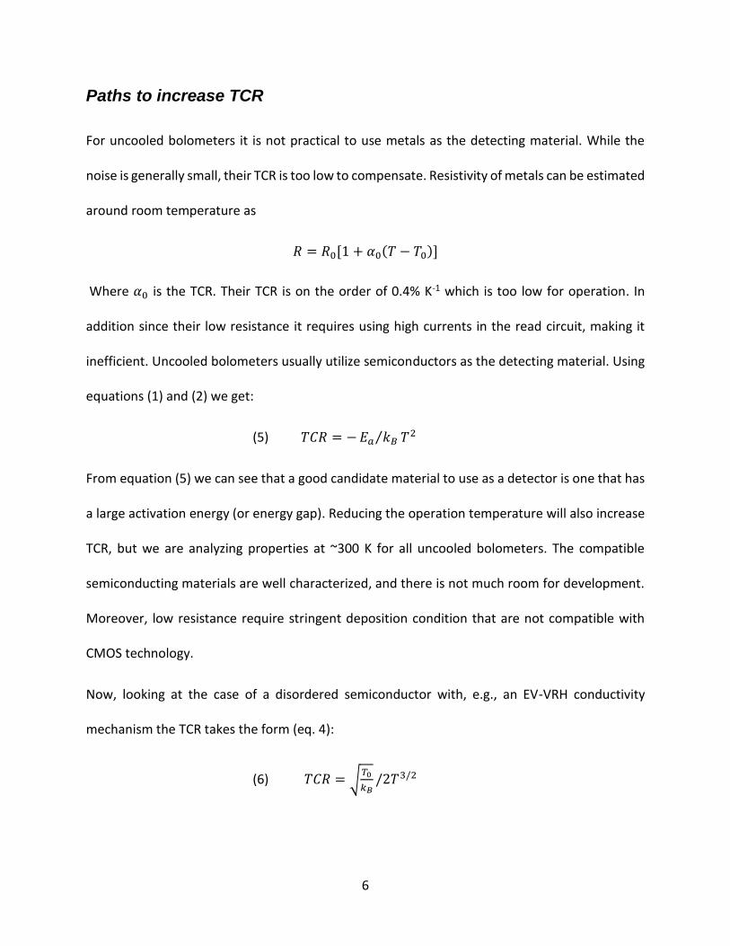
Paths to increase TCR
For uncooled bolometers it is not practical to use metals as the detecting material. While the
noise is generally small, their TCR is too low to compensate. Resistivity of metals can be estimated
around room temperature as
𝑅 = 𝑅0[1 + 𝛼0(𝑇 − 𝑇0)]
Where 𝛼0 is the TCR. Their TCR is on the order of 0.4% K-1 which is too low for operation. In
addition since their low resistance it requires using high currents in the read circuit, making it
inefficient. Uncooled bolometers usually utilize semiconductors as the detecting material. Using
equations (1) and (2) we get:
(5) 𝑇𝐶𝑅 = −𝐸𝑎 𝑘𝐵⁄ 𝑇2
From equation (5) we can see that a good candidate material to use as a detector is one that has
a large activation energy (or energy gap). Reducing the operation temperature will also increase
TCR, but we are analyzing properties at ~300 K for all uncooled bolometers. The compatible
semiconducting materials are well characterized, and there is not much room for development.
Moreover, low resistance require stringent deposition condition that are not compatible with
CMOS technology.
Now, looking at the case of a disordered semiconductor with, e.g., an EV-VRH conductivity
mechanism the TCR takes the form (eq. 4):
(6) 𝑇𝐶𝑅 = √𝑇0
𝑘𝐵/2𝑇3/2
7
We draw attention to two important features. Now the temperature power is 3/2 and not 2, so
at 300K it results in a TCR increase of 10 times. Second, there is an opportunity to improve TCR
by controlling T0. There is still no a-priori method to predict the resulting effect of a specific type
of disorder on these parameters, thus the search may be rather wide, and indeed research groups
apply a variety of approaches. We combined 2 factors that lead to disorder: The first is unique to
this study- we oxidized the samples using an ion beam assisted deposition method. We combined
this with a previously reported method of doping with large transition metal atoms (so they tend
to oxidize) to induce disorder.
Disordered materials usually have high resistance. However high resistance can be overcome by
several methods. First, doping can reduce resistance (e.g. boron doping in amorphous silicon).
Second, annealing treatments can reduce the effective disorder area, meaning only small area in
the sample have high resistance, making the total resistance low but the small areas that possess
high TCR govern the behavior. Another method is changing the geometry in order to achieve
lower effective resistance.
The change in resistance can be a result of a local regions in the film with a high TCR. This can be
achieved by annealing treatments so that the majority of the film will have low resistance (and
low TCR) but because of a connected network of high TCR regions the total film’s TCR can still be
high. In other cases the films are uniform and the resistance change is from all the film. This can
enable fabrication of smaller area active films with similar properties in the bolometer.
8
Deposition
Magnetron Reactive Co-sputtering
Magnetron sputtering is a widely used method to deposit thin films, and especially oxides. It is a
physical vapor deposition (PVD) technique, i.e. ions and aggregates from the material physically
strike the substrate to be coated thus forming a thin film. In sputtering an ideal gas (typically
Argon) is insert to a high vacuum chamber then it is ionized into a plasma and accelerated toward
the material we wish to deposit, which is called a target. The impact of the ions with the target
cause multi-atom aggregates of material to sputter from the target and accumulate on a
substrate (Fig. 2a). In magnetron sputtering a set of magnets are placed below the target which
creates a magnetic field that traps the plasma ions in the vicinity of the target, increasing its
density and stability, and with it the deposition rate and process reliability. When sputtering from
an insulating target charge can accumulate on the surface of the target that will repulse the ions.
This can result in unstable plasma (which will result in unstable deposition) and even extinguish
the plasma entirely. To prevent charge buildup on non-conductive targets a radio frequency AC-
voltage is applied to the target. In addition to Argon, other gasses, such as Nitrogen or Oxygen
can be added to the plasma mixture, and react with the material being deposited. Such
depositions are called reactive sputtering. In our case, there are two ways to insert the reactive
gas to the chamber. One is through a gas-ring near the substrate (Fig 2a). The second method is
via low energy ion source. In this method, gas is ionized and then accelerated toward the
substrate (Fig 2b). This method is called ion beam assisted deposition (IBAD). In our system the
substrate is placed at the top-center of the vacuum chamber, facing downward. The materials’
9
targets are at the bottom perimeter of the chamber, facing concentrically toward the substrate.
The IBAD is placed at the center and bottom of the chamber. Our deposition system is a high-
vacuum magnetron sputtering system (ATC Orion by AJA International, Inc.) with base pressure
of 8 × 10⁻⁹ Torr. For the films that will be presented in this study we used IBAD to insert the oxygen
to the chamber and not the gas-ring (we will discuss in more details the IBAD system later).
It is possible to heat the substrate during the deposition. In our system the substrate holder can
be heated up to 850°C. The substrate holder can rotate during deposition to improve film’s
uniformity on large substrates. The RF/DC sputter guns have a maximum power of 300 W and
600 W respectively and it is possible to deposit from up to three different targets simultaneously
(two RF targets and one DC target). Depositing from more than one target simultaneously is
known as co-sputtering. By changing the power delivered to a target it is possible to control the
rate of the deposition of a material and by that to control the ratio of the materials that
accumulate on the substrate, thus forming the thin film. The rate is measured by a piezoelectric
crystal that can be placed where the substrate is positioned during deposition, thus providing a
reliable rate reading. It is important to notice that when reactive gas is inserted during deposition
it is likely to react with the target material and change the deposition rate in an uncontrolled
manner, and with it the sample composition. This phenomena is called target poisoning and is
the main cause for reproducibility problems in reactive depositions. To overcome this, we
executed rate measurements for each material in the presence of oxygen and only after the rate
was stabilized. Sputtering of all samples was performed at a constant pressure of 3 mtorr in a
controlled mixture of ultra-high purity (UHP) Ar and UHP O2. The partial pressure of oxygen,
between 2% and 12% of the total pressure, was controlled by the relative flow rate of the gasses.
10
The total flow of the gasses was kept constant at 26 SCCM. In our research the thickness of the
samples was set to 100 nm (±10 nm).
Figure 2. a) view of the inside of the high vcuum chamber, showing a target during sputtering with the place of
the gas-ring in opposed to the oxygen IBAD source. b) outside look of the sputtering system, including vacuum
chamber and power supplies.
COPRA Ion-beam assisted deposition
In our study we use a CCR TECHNOLOGY COPRA model DN-160 for the IBAD. It is a filament-less,
radio Frequency (RF) driven, low-pressure plasma source. Gas is inserted via dedicated mass flow
controller to the COPRA and ionized by RF source and a Helmholtz coil, then the plasma is
accelerated from the source toward the substrate by a carbon grid at a 200 V potential (Fig. 3c).
The ion energy does not depend on the RF-power and is constant for any power (Fig. 3a). Instead,
11
the RF-power is changing only the ion current density (Fig 3b). Moreover the plasma beam
produced by the COPRA is quasi-neutral i.e. it contains roughly the same number of ions and
electrons which prevent significant charge buildup. Another essential feature of the COPRA
plasma technology is that for any kind of gas the degree of dissociation is close to 100%. The
COPRA IBAD can be used with reactive gases (like O2 or N2), and when using reactive gasses, IBAD
efficiently provides a source of both ions and highly dissociated (mono-atomic) species, allowing
more efficient oxidation and at lower temperatures [17, 18]. It has also been shown to help
achieve good reproducibility [18]. Furthermore due to the kinetic energy of incoming ions IBAD
is known to produce dense films [18].
Figure 3. a,b) The COPRA IBAD ion beam porperties dependancy of the power applyed [19]. c) IBAD illusstration.
12
Experimental tools and techniques
Substrate and Cleaning
The samples were deposited on 6×6 mm Silicon wafers (1 0 0) with 1 µm of SiO2 layer. The wafers
were cleaned prior to deposition by ultra-sonication of 5 minutes in acetone and isopropanol
then dried by UHP N2 prior to loading into the vacuum chamber’s load-lock.
Structural Characterization
Imaging and thickness
In order to determine the films morphology and grain size we used high resolution scanning
electron microscopy (HRSEM). Our films have high resistance, thus charge can accumulate on the
surface when scanning, which results in high reflection and will prevent achieving the best
resolution. We also used atomic force microscopy (AFM) that is not affected by charging, enabling
to quantify the film roughness. Focused ion beam (FIB) includes also a HRSEM, but in addition it
can use an ion beam to mill through the film and provide a cross section view of the film. Using
FIB we determine the thickness of the films.
Energy-Dispersive X-ray spectroscopy (EDX)
Using EDX it is possible to determine the concentration of a certain element in a sample and the
relative percentage of a few elements. A high energy electron beam hitting the sample causes
excitation of electrons from inner orbitals of an atom. This is followed by emission of x-ray
radiation. Different elements emit different wavelengths according to their orbital energies. The
intensity of the emission is proportional to the amount of element in the sample. In our research
13
we used EDX to verify that the percentage of the elements in our sample are what we intend
them to be in the fabrication process. The measured depth by the EDX is much larger than the
film thickness, which means that it also measured the silicon oxide substrate. Because of that
and because the EDX sensitivity to oxygen is low, it is not possible to determine the oxygen
concentration in the films using EDX.
X-Ray Diffraction (XRD)
XRD is used to characterize the crystal structure of a material. In case of order crystalline
materials, according to Bragg's law, if the path length difference of X-rays scattered from crystal
planes is equal to an integer number of wavelengths and the scattering occurs elastically, then a
constructive interference can take place by the Bragg equation.
n2dsin ()
Where n-integer, -wavelength, d-lattice spacing and - Bragg angle.
By measuring the Bragg angle, extracting the d-space of a certain plane orientation is straight
forward.
In case of finite size polycrystalline films the scattering intensity will be smaller and resulting in a
wider peak.
B(2𝜃) =𝐶𝜆
𝐿𝑐𝑜𝑠𝜃
Where B is the full width at half maximum of the peak and L is the layer thickness or individual
crystal size.
Peak broadening can be also a result of spread in the lattice spacing due to strain effects or in an
amorphous layer. That is because in these cases the distance between crystal sites are different
14
at different areas on the sample, when taking into account that the XRD has a ~1 mm diameter.
Using the XRD it is possible to characterize film phases of growth as a function of fabrication
process parameters.
Rutherford backscattering spectrometry
Rutherford backscattering spectrometry (RBS) is a non-destructive technique used to determine
the structure and composition of materials by measuring the backscattering of a beam of high
energy ions (typically protons or alpha particles) impinging on a sample. This method has a very
good sensitivity for heavy elements of the order of parts-per-million. Moreover, it can show the
concentration of elements in terms of depth with a resolution of a few nanometers. This allowed
us to determine the oxygen concentration in the films with no interference from the silicon oxide.
RBS measurements were conducted to verify with higher precision the stoichiometric ratio
between V, Nb and O, and as a function of depth with ~10 nm resolution. The RBS spectra were
acquired in the Bar Ilan Nano-characterization center with an ULTRATM Silicon-Charged Particle
Detector (ORTEC) and in Cornell geometry. The spectra were collected in a 2.025 MeV 4He+ ±
1Kev beam. The beam current was about 13 nA, with a nominal diameter of 0.5 mm. An electron
suppressor was used between the beam entrance and the sample holder.
Electrical Characterization
Transport measurements
R vs. T measurements were executed in a 2-probe configuration, using high precision electronics
(Keithley source-meter and electrometer). 4-probe resistance configuration was not used, due to
relatively high resistance of the samples. Contacts were wire-bonded directly to the samples that
15
were then measured in our home-made cryostat inside a liquid nitrogen Dewar. This system
allows us to measure resistance in a temperature range from 77K to 370K. A temperature ramp
rate, of 3 K/min (for heating and cooling), resulted in a resolution better than 50 mK (Fig. 5),
providing an accurate measurement of the temperature dependent TCR. We performed at least
three heating and cooling cycles for each sample, to ensure stability and reproducibility. One
problem is that at some point the sample resistance becomes comparable to input impedance of
the voltmeter and then the input impedance limits measurement. Nevertheless, we tested a
number of samples (with reasonable resistance) to rule out possible large interface resistances.
Figure 4. Our resistance vs. temperature measurement system.
Figure 5. Graph of temperature vs. time at heating rate of 3 K/min showing resolution of less than 50 mK.
Heater
Insert
L.N dewier
Temperature
controller
Electrometer
Source-meter
16
Pixels fabrication
Uniformity in terms of resistance and TCR is an important aspect for bolometer arrays. In order
to determine the differences between micro-scale pixels that were deposited together, we
fabricated and measured a number of 20µ×50µm2 pixels in an array (see Figure 6). The pixels
were fabricated by standard lift-off photolithography over the entire substrate; with a pitch of
0.5 mm. I.e. the oxide-alloy is deposited through a pre-defined polymer mask, which is
consequently lifted-off, leaving the pixel pattern. This polymer based method is possible in our
case since the sample is not heated during deposition and the oxygen partial pressure is low. In
order to measure transport properties of the pixels, 150 nm thick vanadium electrodes were
sputter-deposited on the edges of each pixel through another lithography step (Fig. 6).
Figure 6. VxNb1-xOy pixels (appear orange) between V electrode (yellow).
Noise measurements
The main noise with the biggest amplitude in the low frequency range is the flicker noise (1/f
noise). In order to be able to measure it, we needed a wide band amplifier with lower noise than
our samples. Also to be able to measure low frequencies the bandwidth needed to be of at least
1 KHz. We used Signal Recovery 7270 lock-in amplifier, which can measure down to 2 nV. In order
to minimize the noise from external sources the sample was shielded in a metal box and the
17
cables from the sample to the spectrum analyzer were short as possible. Voltage noise
measurement was not possible with our setup because the input impedance of the analyzer is 1
MΩ and our samples are with the same order of resistance or even higher. We preformed current
noise measurements, but found that the noise level of the ground in our lab was very large, and
concealed the information from the sample. The noise was mainly 50Hz (and its harmonics)
electrical noise but since it was broadened, it introduced unwanted interference which prevent
us to measure our samples, even with a 50Hz notch filter. So, in this setup we are not able to
provide reliable noise measurements.
18
Results & Discussion
The effect of IBAD
Figure 7. a) TCR (blue) and resistance (red) as function of IBAD power for VOx samples with no Nb and with 8%
oxygen in the gas mixture. b) TCR (blue) and resistance (red) as function of IBAD power for VxHf1-xOy samples with
20% Hf and with 2% oxygen in the gas mixture.
Figure 7a shows the square resistance and TCR at 300 K of vanadium oxide films that were
deposited at room temperature with 8% partial pressure of oxygen in the argon-oxygen gas
mixture, versus different IBAD power input. While the resistance keeps increasing with the
increased IBAD power the TCR increase and then saturate at -2.5% K-1. Nevertheless it shows that
19
TCR can be increase by IBAD in a controlled manner even at room temperature. Figure 7b shows
the square resistance and TCR at 300 K of vanadium hafnium oxide alloy films that were
deposited at room temperature with low partial pressure of oxygen of 2%. In this case the TCR is
not saturated and it increase by 75% while the square resistance is slightly more than double.
With fine tuning of oxygen partial pressure and IBAD power it will be possible to achieve even
better TCR-resistance ratios.
As shown in previous works, doping by large atoms can increase the TCR of vanadium oxide thin
films [12, 20]; we studied niobium doped vanadium oxide alloy as well as hafnium doped
vanadium oxide alloy in the presence of IBAD. First we characterize the TCR and square resistance
versus oxygen percentage in the chamber at 300 K of vanadium-niobium oxide alloy with 8%
niobium in vanadium and 300 W IBAD power, see Fig. 8. The resistance is higher for higher
percentage of oxygen and the TCR increases to values even higher than -3% K-1. The best rang of
oxygen seems to be between 4%-8%, while above 8% the resistance continues to increase with
only minor contribution to the TCR.
Figure 8. TCR and resistance (insert) as function of percentage of oxygen in the total gas mixture and with 300 W
IBAD power.
20
Structural properties
We emphasize that the deposition rate for each element was measured before every deposition
and was done with the intended oxygen concentration, verifying that the rate is stable before
starting deposition. But we couldn’t know what the final phase of vanadium\niobium\hafnium
oxide will accumulate on the substrate a-priori, especially the total level of oxidation, which will
determine also the film thickness. Therefore there was a need to calibrate a factor for each
material. As it can be seen in Fig 9a before calibration the thickness of the deposited layer was
much higher than the planned 100 nm. But after calibration we do get to 100 nm (±10 nm) as can
be seen in Figs 9b and 9c.
RBS measurements (Figs. 10a,b) shows that the fraction of Nb in V is constant throughout the
whole deposited layer and it also confirm it to be in par with the nominal rate measured prior to
deposition. For example, the RBS extracted stoichiometric ratio V: Nb : O in the sample with
nominally 20% Nb is 4 : 1 : 6 and in the 70% Nb sample is 1 : 2.4 : 7, giving 20% and 70.6% Nb,
respectively. The RBS beam diameter is about 0.5 mm, therefore we use EDX to verify that the
ratio is constant at smaller scale which is important for bolometer arrays. The area that was
Figure 9. a) FIB measurements shownig thickness of VOx sample with 300 W IBAD and 8% partial pressure of O2,
before rate clibration b) Thickness of VxNb1-xOy with 3% Nb, 8% partial pressure of O2 and 450 W IBAD, affter
clibration c) rate measurment calibration. c) Thickness of VxNb1-xOy with 8% Nb, 4% partial pressure of O2 and 0 W
IBAD, after calibration.
21
measure was 50µ×50µ m2 and it shows that the stoichiometric ratio of the V-Nb is indeed
constant up to a difference of 2%, which is smaller than the measurement error (Fig. 10c,d). XRD
measurements of all the compositions (Fig. 11) showed amorphous growth with no preferred
phase.
Figure 10. Stoichiometry measurements using RBS (a,b) and EDX (c,d) of two samples one with expected 20% of
Nb in V (a,c) and the second is with expected 70% of Nb in V (b,d). The EDX measurement were conducted on a
30 µm x 30 µm area and each spot is in a distance of 100 µm from the previous spot. RBS measurements show
stoichiometry uniformity in term of depth.
22
HRSEM imaging of the surface taken at different positions on the samples show a smooth surface
and small grains (Fig. 12a,b). Because of the relatively high resistance of the samples that cause
charge to accumulate on the surface, it was difficult to focus and achieve the best resolution.
AFM measurements (Fig. 12c,d) for various samples show small grains size of less than 10 nm and
a very low roughness of maximum 0.96 nm RMS.
Figure 12. a,b) SEM measurements showing small grains and smooth surface. c,d) AFM measurements for various
samples shows very low roughness rms of 0.96 nm and grains size of less than 10 nm. Note the full height color
scale is 2.7nm.
Figure 11. a) XRD measurements showing amorphous growth with no preferred phase for various samples.
23
Transport properties
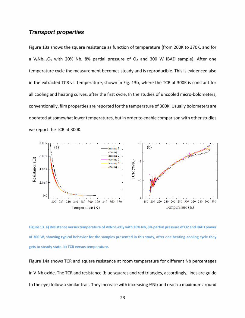
Figure 13a shows the square resistance as function of temperature (from 200K to 370K, and for
a VxNb1-xOy with 20% Nb, 8% partial pressure of O2 and 300 W IBAD sample). After one
temperature cycle the measurement becomes steady and is reproducible. This is evidenced also
in the extracted TCR vs. temperature, shown in Fig. 13b, where the TCR at 300K is constant for
all cooling and heating curves, after the first cycle. In the studies of uncooled micro-bolometers,
conventionally, film properties are reported for the temperature of 300K. Usually bolometers are
operated at somewhat lower temperatures, but in order to enable comparison with other studies
we report the TCR at 300K.
Figure 13. a) Resistance versus temperature of VxNb1-xOy with 20% Nb, 8% partial pressure of O2 and IBAD power
of 300 W, showing typical behavior for the samples presented in this study, after one heating-cooling cycle they
gets to steady state. b) TCR versus temperature.
Figure 14a shows TCR and square resistance at room temperature for different Nb percentages
in V-Nb oxide. The TCR and resistance (blue squares and red triangles, accordingly, lines are guide
to the eye) follow a similar trait. They increase with increasing %Nb and reach a maximum around
24
50% Nb (a bit lower for the TCR). Afterward, both decrease yet the TCR drops rapidly reaching
below -1% K-1 for only Nb, relative to -2.5% K-1 for Vanadium. The parameters that seem most
suitable for micro-bolometers use is up to 20% Nb where TCR reaches values as high as -3.5% K-
1. Above 20% Nb the TCR still increases, yet the square resistance may be too high. The VxHf1-xOy
alloy shows somewhat different behavior (Fig. 14b). Above 40% Hf the square resistance is too
high for us to measure and remains this way up to 100% Hf. This is likely because hafnium oxide
is an insulator with band gap of 5.3-5.7 eV (for the most common phase HfO2), while the Niobium
oxide is well known semiconductor with band gap size of about 3.4 eV (for the most common
phase Nb22O5). Interestingly, at low doping concentrations the VxHf1-xOy and the VxNb1-xOy alloys
reach similar resistance values for similar doping levels. But the VxHf1-xOy alloy shows slightly
higher TCR than the VxNb1-xOy alloy relative to the square resistance, for example for square
resistance of 17 MΩ/sq the VxNb1-xOy alloy have TCR of 3.2% K-1 while the VxHf1-xOy alloy have
TCR of 3.4% K-1 for 10 MΩ/sq. These results make the Hf doped films more suitable material for
bolometer sensor applications.
25
Figure 14 Figure 15 a) Resistance (red) and TCR (blue) versus Nb percentage in the V-Nb-O mixture, for 8% of
oxygen in the gas mixture. The samples are 100 nm thick and were deposited at room temperature using IBAD
power of 300 W. b) Resistance (red) and TCR (blue) versus Hf percentage in the V-Hf-O mixture, for 6% of oxygen
in the gas mixture. The samples are 100 nm thick and were deposited at room temperature using IBAD power of
300 W.
26
The film uniformity is evidenced in the measurements and characterization of a set of 50 µm ×
20 µm pixels measured at room temperature, see Fig. 14a,b. To better assess the uniformity we
show the deviations, in percentage, of a quantity (resistance or TCR) from its average value, in
Fig. 14a for the resistance and in Fig. 14b for the TCR. These results are excellent compared to
bolometer arrays in use today, where the typical deviation of the resistance between pixels in
the array is on the order of 100%. These results show that fabrication process with oxygen
through IBAD can help simplify the readout circuit of a bolometers array [21].
Figure 16. a,b) Resistance and TCR deviation from the average of each pixel at room temperature of 8.5% Nb in V
pixels, the sample deposited at room temperature with 4% of oxygen in the gas mixture and 300W COPRA power.
27
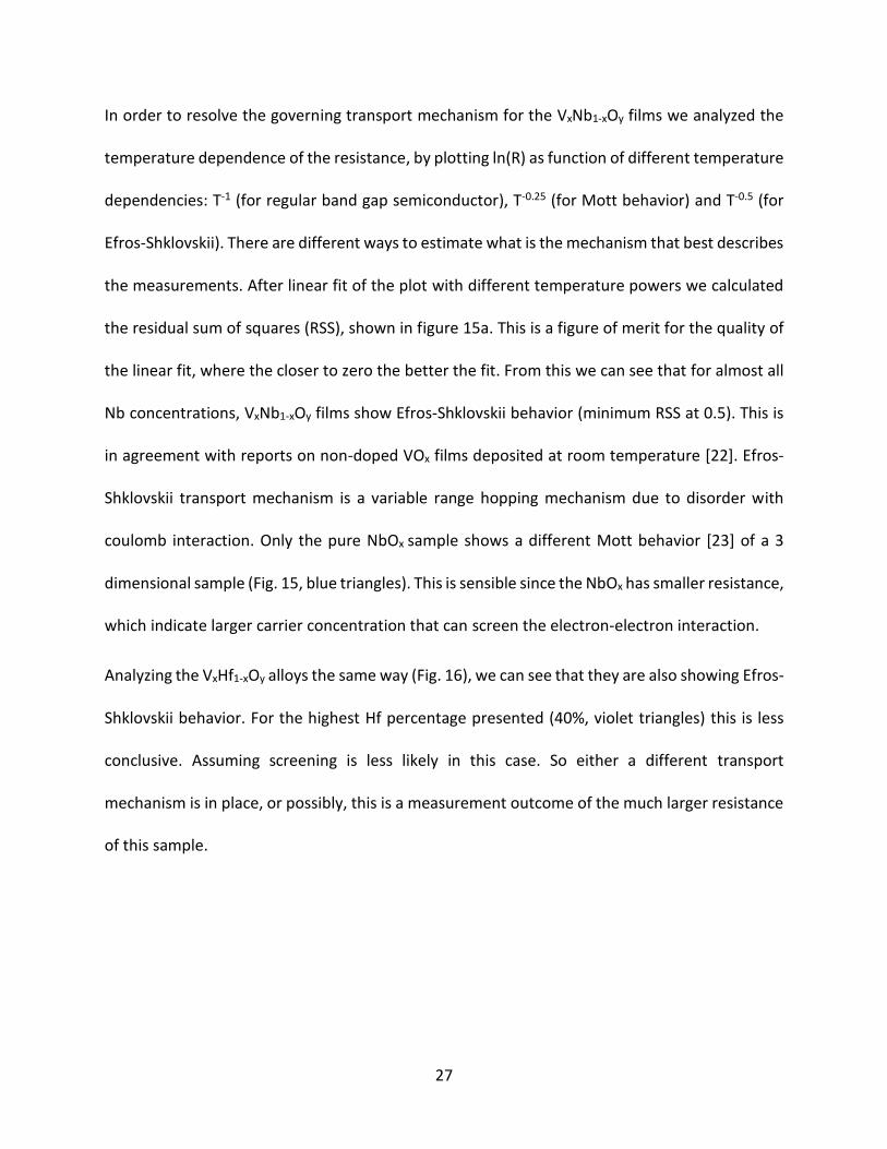
In order to resolve the governing transport mechanism for the VxNb1-xOy films we analyzed the
temperature dependence of the resistance, by plotting ln(R) as function of different temperature
dependencies: T-1 (for regular band gap semiconductor), T-0.25 (for Mott behavior) and T-0.5 (for
Efros-Shklovskii). There are different ways to estimate what is the mechanism that best describes
the measurements. After linear fit of the plot with different temperature powers we calculated
the residual sum of squares (RSS), shown in figure 15a. This is a figure of merit for the quality of
the linear fit, where the closer to zero the better the fit. From this we can see that for almost all
Nb concentrations, VxNb1-xOy films show Efros-Shklovskii behavior (minimum RSS at 0.5). This is
in agreement with reports on non-doped VOx films deposited at room temperature [22]. Efros-
Shklovskii transport mechanism is a variable range hopping mechanism due to disorder with
coulomb interaction. Only the pure NbOx sample shows a different Mott behavior [23] of a 3
dimensional sample (Fig. 15, blue triangles). This is sensible since the NbOx has smaller resistance,
which indicate larger carrier concentration that can screen the electron-electron interaction.
Analyzing the VxHf1-xOy alloys the same way (Fig. 16), we can see that they are also showing Efros-
Shklovskii behavior. For the highest Hf percentage presented (40%, violet triangles) this is less
conclusive. Assuming screening is less likely in this case. So either a different transport
mechanism is in place, or possibly, this is a measurement outcome of the much larger resistance
of this sample.
28
Figure 17. a) Residual sum of squares showing the best fit for ‘p’ for samples with different percentage of Nb in
the VxNb1-xOy mixture. b) Linear fit for p=1/2 for VOx sample, indicating on Efros-Shklovskii variable range hopping
conductance mechanism. c) Linear fit for p=1/4 for NbOx sample, indicating on Mott variable range hopping
conductance mechanism.
Figure 18. Residual sum of squares showing the best fit for the resistance power for samples with different
percentage of Hf in the VxHf1-xOy mixture.
29
Summary
We presented a novel fabrication method of doped vanadium oxide that enables efficient and
well-controlled room temperature deposition for uncooled micro bolometer applications. We
showed that IBAD oxidation improves TCR for vanadium or vanadium based alloy during the
deposition. The oxygen inserted via the IBAD is ionized which reduces the need for heat
treatments as opposed to what is in use today. This will simplify the process and lower costs,
since it can enable to perform the deposition in standard foundries. Furthermore, we showed
that oxidation using IBAD can increase the TCR of a material. In addition by changing the power
of the IBAD it is possible to control the resistance and TCR. Although the samples square
resistance was higher than what is commonly in use today, we show that uniformity in terms of
TCR and resistance, even at micro-scale and a cross a few millimeters, are on the order of a few
percent. This is much better than in today’s bolometer arrays, where changes of 100% in
resistances between pixels is common. Such uniformity will help simplify the readout circuit,
which has to be able to handle the large changes in resistivity and fluctuation in TCR. This will
additionally simply fabrication processes and further lower the fabrication costs. The samples
have very low RMS roughness of less than 1 nm and XRD measurement showed amorphous
growth with no preferred phase. Also we showed that the transport mechanism, for samples that
were fabricated using our method, is Efros-Shklovskii variable range hoping, which indicates high
disorder with electron-electron interaction.
Both vanadium based alloys, VxNb1-xOy and VxHf1-xOy that were fabricated using our method
showed significant increase of the TCR relatively to regular VOx. Comparison between the two
30
alloys shows advantage of the VxHf1-xOy alloy in terms of TCR to resistance ratio over the VxNb1-
xOy alloy. For example VxHf1-xOy sample with resistance of 10 MΩ have a TCR of -3.4 K-1, in oppose
to VxNb1-xOy sample that have higher resistance of 17 MΩ but lower TCR of -3.2 K-1 (both were
deposited with the same IBAD power of 300 W). We note that the properties presented here can
be further optimized for a specific application mainly by controlling the oxygen partial pressure,
IBAD power and doping level. It is therefore probable that better results, i.e. a higher TCR to
resistance ratio, can be attained with optimized process parameters. Moreover, the high square
resistance can be overcome by modifying the device geometry of the bolometer.
Further studies in a full bolometer geometry are needed in order to extract the actual efficiency
of micro-bolometers arrays that are based on our fabrication method.
31
Bibliography
1. Yoneoka, S., et al. ALD-metal uncooled bolometer. in Micro Electro Mechanical Systems (MEMS), 2011 IEEE 24th International Conference on. 2011. IEEE.
2. Finot, E., et al. Raman and photothermal spectroscopies for explosive detection. in SPIE Defense, Security, and Sensing. 2013. International Society for Optics and Photonics.
3. Rogalski, A., Recent progress in infrared detector technologies. Infrared Physics & Technology, 2011. 54(3): p. 136-154.
4. Han, Y.H., et al., Properties of electrical conductivity of amorphous tungsten-doped vanadium oxide for uncooled microbolometers, in Advances in Nanomaterials and Processing, Pts 1 and 2, B.T. Ahn, et al., Editors. 2007, Trans Tech Publications Ltd: Stafa-Zurich. p. 343-346.
5. Subrahmanyam, A., Y.B.K. Reddy, and C.L. Nagendra, Nano-vanadium oxide thin films in mixed phase for microbolometer applications. Journal of Physics D: Applied Physics, 2008. 41(19): p. 195108.
6. Ozcelik, A., et al., Vanadium oxide thin films alloyed with Ti, Zr, Nb, and Mo for uncooled infrared imaging applications. Journal of Electronic Materials, 2013. 42(5): p. 901-905.
7. Venkatasubramanian, C., M.W. Horn, and S. Ashok, Ion implantation studies on VOx films prepared by pulsed dc reactive sputtering. Nuclear Instruments and Methods in Physics Research Section B: Beam Interactions with Materials and Atoms, 2009. 267(8–9): p. 1476-1479.
8. Soltani, M., et al., Effects of Ti--W codoping on the optical and electrical switching of vanadium dioxide thin films grown by a reactive pulsed laser deposition. Applied Physics Letters, 2004. 85(11): p. 1958-1960.
9. Gauntt, B.D., et al., Disordered Vanadium Oxide Thin Films for Use in Infrared Detection. Microscopy and Microanalysis, 2008. 14(2): p. 236-237.
10. Fieldhouse, N., et al., Vanadium oxide thin films for bolometric applications deposited by reactive pulsed dc sputtering. Journal of Vacuum Science & Technology A: Vacuum, Surfaces, and Films, 2009. 27(4): p. 951-955.
11. Cabarcos, O.M., et al. Comparison of ion beam and magnetron sputtered vanadium oxide thin films for uncooled IR imaging. in SPIE Defense, Security, and Sensing. 2011. International Society for Optics and Photonics.
12. Nam, S.-P., et al., Electrical properties of vanadium tungsten oxide thin films. Materials Research Bulletin, 2010. 45(3): p. 291-294.
13. Li, C., C.J. Han, and G. Skidmore, Overview of DRS uncooled VOx infrared detector development. Optical Engineering, 2011. 50(6): p. 061017-061017.
14. Anderson, P.W., Absence of Diffusion in Certain Random Lattices. Physical Review, 1958. 109(5): p. 1492-1505.
15. Mott, N.F., Electrons in disordered structures. Advances in Physics, 1967. 16(61): p. 49-144. 16. Efros, A. and B. Shklovskii, Coulomb gap and low temperature conductivity of disordered systems.
Journal of Physics C: Solid State Physics, 1975. 8(4): p. L49-L51. 17. Zijlstra, T., et al., Epitaxial aluminum nitride tunnel barriers grown by nitridation with a plasma
source. Applied Physics Letters, 2007. 91(23): p. 233102-233102. 18. Weiler, M., et al., Deposition of tetrahedral hydrogenated amorphous carbon using a novel
electron cyclotron wave resonance reactor. Applied Physics Letters, 1998. 72(11): p. 1314-1316. 19. CCR TECHNOLOGY, Basics of the COPRA, Retrived from: http://www.ccrtechnology.de/basics.php.
20. Yong Hee, H., et al., Properties of electrical conductivity of amorphous tungsten-doped vanadium oxide for uncooled microbolometers. Diffusion and Defect Data Part B (Solid State Phenomena), 2007. 124-126: p. 343-346.
21. Bhan, R., et al., Uncooled Infrared Microbolometer Arrays and their Characterisation Techniques (Review Paper). Defence Science Journal, 2009. 59(6): p. 580-589.
22. Bharadwaja, S.S.N., et al., Low temperature charge carrier hopping transport mechanism in vanadium oxide thin films grown using pulsed dc sputtering. Applied Physics Letters, 2009. 94(22): p. 222110-222110.
23. Mott, N.F., Conduction in glasses containing transition metal ions. Journal of Non-Crystalline Solids, 1968. 1(1): p. 1-17.
א
תקציר
ותשתית לחימה אמצעי פיתוח, למחקר המינהלמחקר זה בוצע במסגרת פרוייקט משותף של מפא"ת )
. מטרת הפרוייקט היא לפתח חיישן מוזל לחישה SCD Inc. (SemiConductor Devices)( ו טכנולוגית