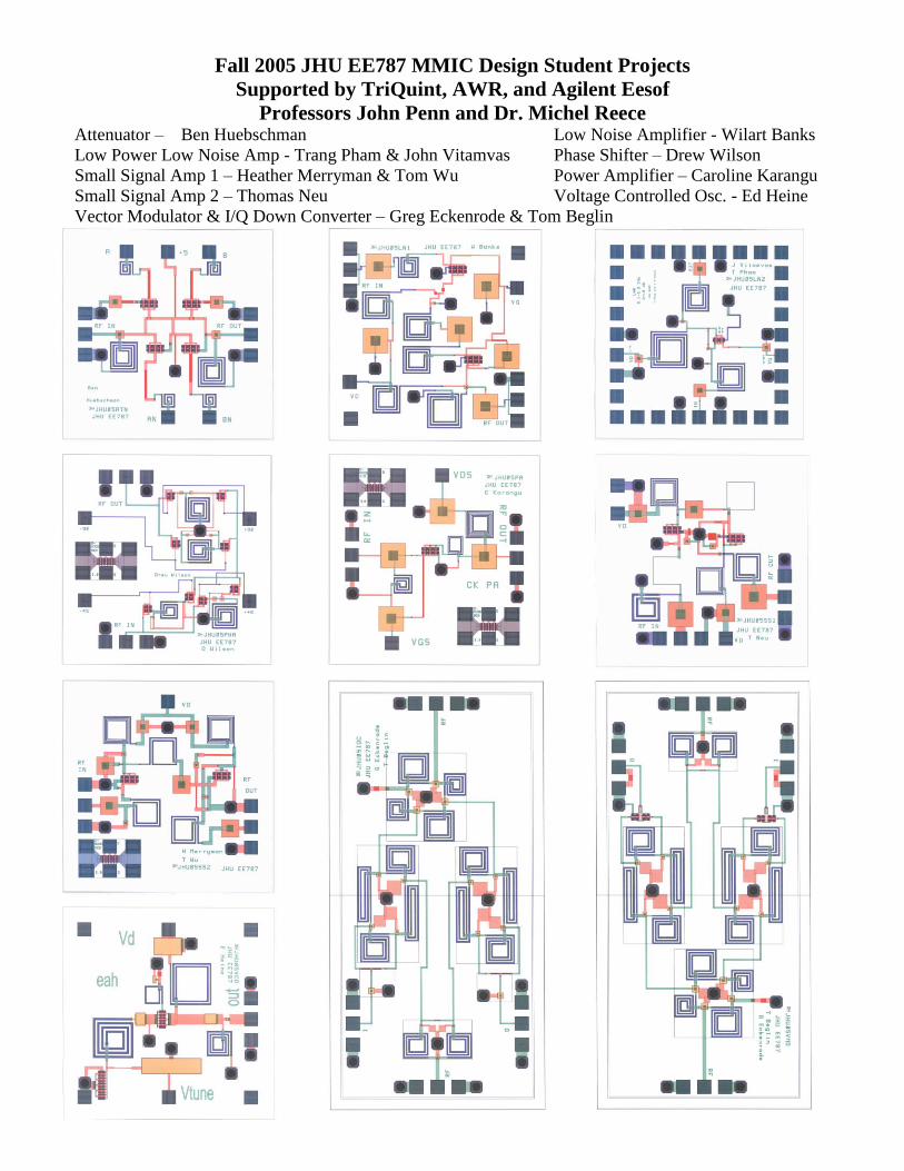
Fall 2005 JHU EE787 MMIC Design Student Projects Supported by TriQuint, AWR, and Agilent Eesof Professors John Penn and Dr. Michel Reece Attenuator – Ben Huebschman Low Noise Amplifier - Wilart Banks Low Power Low Noise Amp - Trang Pham & John Vitamvas Phase Shifter – Drew Wilson Small Signal Amp 1 – Heather Merryman & Tom Wu Power Amplifier – Caroline Karangu Small Signal Amp 2 – Thomas Neu Voltage Controlled Osc. - Ed Heine Vector Modulator & I/Q Down Converter – Greg Eckenrode & Tom Beglin
Transcript
Fall 2005 JHU EE787 MMIC Design Student Projects
Supported by TriQuint, AWR, and Agilent Eesof
Professors John Penn and Dr. Michel Reece Attenuator – Ben Huebschman Low Noise Amplifier - Wilart Banks
Low Power Low Noise Amp - Trang Pham & John Vitamvas Phase Shifter – Drew Wilson
Small Signal Amp 1 – Heather Merryman & Tom Wu Power Amplifier – Caroline Karangu
Small Signal Amp 2 – Thomas Neu Voltage Controlled Osc. - Ed Heine
Vector Modulator & I/Q Down Converter – Greg Eckenrode & Tom Beglin
Digitally Controlled C Band Attenuator
By
Benjamin D. Huebschman
Microwave Monolithic Integrated Circuit (MMIC) Course Johns Hopkins University
Fall 2005
Abstract A digitally controlled attenuator operating over a frequency band from 5150 MHz to
5875 MHz is described in this paper. The circuit was designed and modeled using the
Advanced Design System (ADS) software package by Agilent. The design technique
allowed for very precise selection of attenuation. The simulations of the circuit showed
stable performance across a broad frequency band. A layout for a physical design was
also completed as part of the project.
Introduction
The description of this project will start with the list of specifications. I will then outline
the designs considered for the project and the reason behind the one selected. The
procedures used to finalize this design and implement the layout will be discussed. I will
conclude with the simulation results and a plan for testing the circuit.
Numerous systems require precisely controlled power levels at different points in the
system. One way to accomplish this is a variable attenuator. The specifications for the
digital attenuator describe in this paper are shown below in Table 1.
FREQUENCY 5150 to 5875 MHz
BANDWIDTH > 800 MHz
INSERTION LOSS < 3 dB min IL (2 dB goal)
POWER HANDLING > +10 dBm @ 1 dB compression
VSWR, 50 Ohm < 1.5:1 input & output
SUPPLY VOLTAGE + 5 Volts
CONTROL TTL
SIZE 60 x 60 mil ANACHIP
Table 1. Circuit Requirements
In addition to these listed requirements, the attenuation is required to range from 0 dB to
6dB in four 2 dB steps. It should be mentioned that the insertion loss of the system,
which is a built in attenuation, will be added to the variable attenuation.
Design Approach
Before discussing the mechanism for switching between attenuation levels, the method of
attenuation must be looked at. A good attenuator should match perfectly to 50 Ohms and
reduce the RF power by an arbitrary amount. Fortunately there are two well know
designs for achieving these requirements shown in Figure 1.
Figure 1. Designs for attenuators matched to 50 Ohms
The design on left was chosen because it requires only one via. These are the equations
for determining R1, R2, and R3:
R1 = R2 = Z0 JK - 1K + 1 Eqn. 1 N
R3 = 2 * Z0 JKK2 - 1N Eqn. 2
K is the attenuation level.
With the attenuator design we can move on to the method of control for the circuit. A
number of designs were considered as possible mechanisms to allow for the switching
between circuits. The first is shown in Figure 2. It is the most straight forward, but it
also has a large number of components.
-4dB-2dB
AB Figure 2. Possible designs for variable attenuator
Although this circuit might meet the requirements, it is needlessly complex and the large
number of components could dissipate too much power to satisfy the insertion loss
requirement. Figure 3 shows a much simpler design. Unfortunately, when the switch is
closed, the 50 ohm line is in parallel with the attenuator. This has a resistance between
one hundred and two hundred ohms. When put in parallel with the 50 ohm transmission
line this results in an appreciable amount of attenuation. I was unable to meet the
insertion loss requirements with this design.
This was overcome by inserting a switch between the attenuator and ground. The basic
schematic for the switched is shown in Figure 4.
Figure 3. Simplified Circuit Figure 4. Final Attenuator
Prior to testing the circuit shown in Figure 3, the transistor was evaluated. The default
transistor from the Triquint pallet showed low resistance, power handling over what is
required by the circuit, and a small flat attenuation over the bandwidth of interest.
Using TTL logic, the on state has a minimum voltage of 2.0 V and the off state has a
maximum voltage of 0.8 V. This means that there can be a maximum of 1.2 volts
between the switch being open and into saturation. The circuit needs to perform well at
these worst case values, and this performance cannot change significantly over the range
of voltage allowed by the parameters of TTL logic. The transistor’s S-parameters were
measured at 0 volts and –1.2 volts. It turned out that it did perform well at the these
values.
To meet all the requirements, the VSWR had to be made as small as possible. A simple
two element matching network was added to the input and output. Blocking inductors
were needed to isolate the gate from the RF line. A resistor that shifts the voltage into
compliance levels for TTL was added. This elements are shown later in the report in the
final circuit design.
The design and simulation of the circuit was an iterative process. The first simulation
was done to verify the calculated values of the resistors. Several basic circuit layouts
were simulated. The design gradually increased in complexity as more elements were
added to comply with specifications. The next section will discuss the results of the
simulation of the final circuit.
Simulations
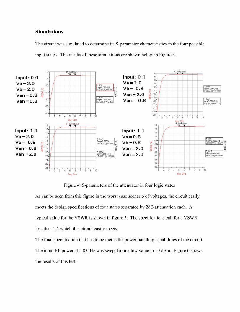
The circuit was simulated to determine its S-parameter characteristics in the four possible
input states. The results of these simulations are shown below in Figure 4.
Figure 4. S-parameters of the attenuator in four logic states
As can be seen from this figure in the worst case scenario of voltages, the circuit easily
meets the design specifications of four states separated by 2dB attenuation each. A
typical value for the VSWR is shown in figure 5. The specifications call for a VSWR
less than 1.5 which this circuit easily meets.
The final specification that has to be met is the power handling capabilities of the circuit.
The input RF power at 5.8 GHz was swept from a low value to 10 dBm. Figure 6 shows
the results of this test.
5 64 7
1.4
1.8
1.0
2.0
freq, GHz
VS
WR
1
Figure 5. VSWR of the circuit
Iin figure 6, the linearity of the circuit begins to break down near the limit. It
should be noted that the output power is plotted on the horizontal axis and that the
input power should be increased by the attenuation level.
-10 -5 0 5 10-15 15
-2.8
-2.7
-2.6
-2.5
-2.9
-2.4
Fund. Output Power, dBm
m1m2
Transducer Power Gain, dB
Figure 6. Power Sweep
The DC performance of the circuit was simulated. The circuit draws very little
current. During the design, it became obvious that the voltage level of the circuit
would have to be shifted in order to allow it to be driven by TTL. The results of
the DC simulation are shown in Figure 7.
Figure 6. DC annotated Circuit layout.
The next section will discuss the components of the layout.
Schematic
Figure 7 shows the annotated DC solution with the components of the circuit labeled.
Figure 7. Annotated Layout of the circuit.
A. Matching network
B. Through switch and control pad
C. Voltage shifter
D. Attenuator switch and control pad
Layout
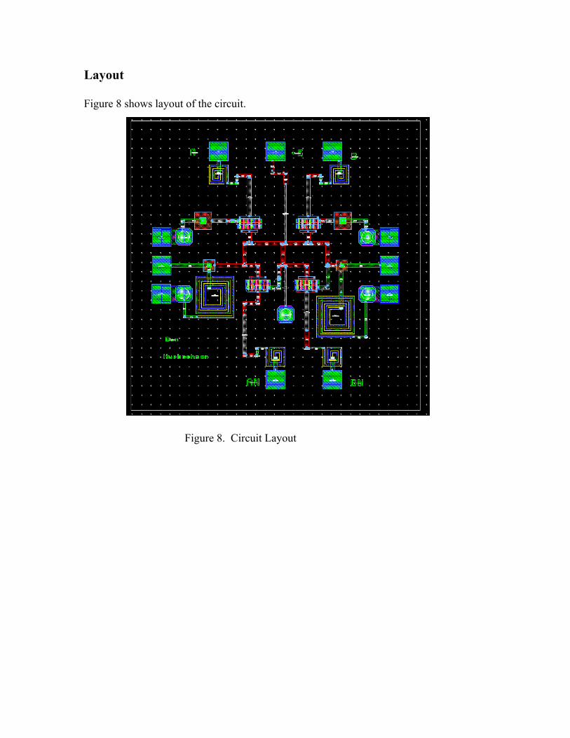
Figure 8 shows layout of the circuit.
Figure 8. Circuit Layout
Test Plan
To thoroughly test the circuit, we would need a vector network analyzer, a mechanism for
measuring power, and DC power sources to bias the circuit. If we are just interested in
validating the attenuation, the power measurement system is unnecessary. The test will
begin by connect the DC bias and the network analyzer. S-parameters for each of the
four logic states would be measured. From these we could extract attenuation and
VSWR. To test the power response of the system, the vector network analyzer would
have to be replaced by the power source at the desired frequency and a power meter. The
power would then be increased until we began to observe changes in the attenuation.
Summary
This paper describes the design procedure and layout of a digitally controlled variable
attenuator. The circuit fulfills are design requirements and specifications. It consumes
virtually no DC power. It uses as a power source a +5 V DC input, but this could be
reduced to +2 V. The circuit could easily be redesigned to have any number of steps or
an arbitrary attenuation level. As the voltage requirements for the transistors decreases,
the required voltage of the DC power could be reduced appropriately. This basic design
Schematic Diagrams ................................................................................................... 9 Final Layout .............................................................................................................. 11 Test Plan.................................................................................................................... 12 Summary and conclusion.......................................................................................... 13
2 of 13
Abstract The design described in this document is a C-band, low-power low noise amplifier (LNA). It has a DC power consumption of 6.34mW at 1.7V and 3.73mA drain bias. It is layed-out to use dual supplies to aid in-lab tweaking of the bias of the 140um depletion-mode FET. The LNA has an operating band of approximately 5.15GHz to 5.875GHz. Within this band the noise figure is less than 2.35dB. Gain is better than 8.5dB across the band with port match better than -15dB. The amplifier is unconditionally stable from near-DC to 10GHz. The amplifier layout is inserted into a 60 mil by 60 mil Anachip for ease of fabrication.
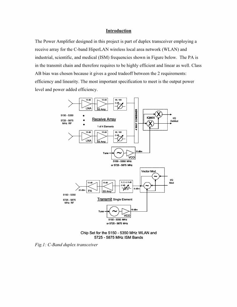
Introduction This LNA is designed the TriQuint TQPED process with vias. The LNA is part of the MMIC design class’ duplex transceiver utilizing a receive array for the C-band HiperLAN wireless local area network (WLAN). It is one of nine unique MMIC designs which make up the C-band transceiver. Each design was to be contained on a 60 mil square die.
Circuit Description The LNA circuit design selected was a single-stage amplifier using a 35um x 4 (140um) depletion mode FET. A drain-gate resistor-capacitor feedback network was used to stabilize the amplifier and flatten the gain but restrict DC current flow from gate to drain. Dual sources are used to bias the amplifier. The DC sources are isolated from the RF network using on-chip inductors and filtering is provided by on-chip bypass capacitors.
3 of 13
Design Philosophy and Design Tradeoffs A single depletion mode FET was chosen because of the desire for an ultra-low-power amplifier with low noise figure. The goal was lower than 10mW of total DC power consumed with a secondary goal of 5mW. Better than 2.5dB noise figure was desired. The first cut design aimed for 5mW of total DC power while achieving 10dB of gain and an unconditionally stable circuit from DC to 10GHz. The decision was made early on to not adopt a single-supply self-biased amplifier. The main reason for this is we suspected the design would be very sensitive to bias and process shifts and wanted the ability to tune in-lab to achieve best performance. Further iterations of this design could implement a self-bias scheme with a single supply to simplify integration. The amplifier was designed to have a low noise figure and low DC power consumption. This dictates a very small device, which inherently will have low, narrow-band gain and be difficult to match (high VSWR). We mitigated this later in the design by bumping DC power slightly (by up-sizing the FET slightly) to improve VSWR. Initial designs showed high gain but very poor VSWR when using a drain-only resistive stabilization. A small series inductor on the FET source combined with an RC feedback stabilization network flattened gain (at the expense of peak gain) and achieved an unconditionally stable design. The LNA is matched for optimum noise figure on the input side using an LC network. The output is matched for VSWR at 50 ohms using an LC network. Both networks are entirely on-chip and neither includes any DC paths to ground, maintaining a low-power operation. Because this design was somewhat new, no hard specifications were provided so reasonable goals were set by the design team. Table 1 – Specification Matrix Spec Specification Goal Layout Schematic Frequency Bandwidth 5150-5875 5150-5875 Gain > 8dB 8.5dB minimum Gain Ripple +/- .5dB max 1.2dB VSWR, 50 ohm <1.5:1 <1.5:1, output
< 1.78:1, input Supply Voltage None specified Dual supplies Noise Figure < 2.5dB < 2.32 dB DC Power <10 mW 6.34mW
4 of 13
Predicted RF Performance The following plots show the predicted performance of the amplifier as layed-out including interconnect, bond pads and bond wires to connect to external supplies. Performance is expected to be slightly better if the RF pads are probed using G-S-G probes and efforts are made to keep inductance to a minimum. Figure 1 – Noise Figure
5.3 5.4 5.5 5.6 5.7 5.85.2 5.9
2.1
2.2
2.3
2.4
2.0
2.5
freq, GHz
m4
NFmin
m4freq=nf(2)=2.310
5.850GHz
2 3 4 5 6 7 8 91 10
2.1
2.2
2.3
2.4
2.0
2.5
freq, GHz
m4
m8
NFmin
m4freq=nf(2)=2.241
5.100GHz
m8freq=nf(2)=2.320
5.900GHznf(2)
nf(2)
5 of 13
Figure 2a – S-parameters
5.3 5.4 5.5 5.6 5.7 5.85.2 5.9
-35
-30
-25
-20
-15
-10
-5
-40
0
freq, GHz
dB(S(2,2))
dB(S(1,1))
dB(S(1,2))
dB(S(1,2))
Figure 2b – S-parameters expanded
2 3 4 5 6 7 8 91 10
-35
-30
-25
-20
-15
-10
-5
-40
0
freq, GHz
dB(S(2,2)) m5
m6
dB(S(1,1))
m5freq=dB(S(2,2))=-14.959
5.100GHzm6freq=dB(S(2,2))=-17.924
5.900GHz
6 of 13
Figure 3a – In-band Gain
5.3 5.4 5.5 5.6 5.7 5.85.2 5.9
8.5
9.0
9.5
10.0
10.5
11.0
11.5
8.0
12.0
m3
m3freq=dB(S(2,1))=8.856
5.850GHz
freq, GHz
dB(S(2,1))
freq, GHz
dB(S(2,1))
Figure 3b – Gain expanded
2 3 4 5 6 7 8 91 10
8.5
9.0
9.5
10.0
10.5
11.0
11.5
8.0
12.0
m3
m7
m3freq=dB(S(2,1))=10.116
5.100GHzm7freq=dB(S(2,1))=8.743
5.900GHz
7 of 13
Figure 4a – In-band Stability
5.3 5.4 5.5 5.6 5.7 5.85.2 5.9
1.5
1.6
1.7
1.4
1.8
freq, GHz
MuPrime1
Mu1
Mu1
Figure 4b – Stability expanded
2 3 4 5 6 7 8 91 10
1.2
1.4
1.6
1.0
1.8
freq, GHz
MuPrime1
8 of 13
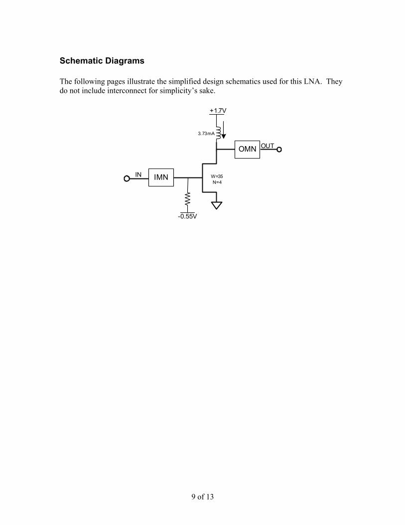
Schematic Diagrams The following pages illustrate the simplified design schematics used for this LNA. They do not include interconnect for simplicity’s sake.
+1.7V
-0.55V
3.73mA
IMN
OMN
IN
OUT
W=35N=4
9 of 13
Figure 5 – Schematic diagram with DC annotation.
0 V
1.68 V
1.68 V
1.68 V
1.68 V
1.68 V
1.68 V
1.68 V
1.68 V
1.68 V
1.68 V 1.68 V
1.68 V
0 V
0 V
0 V0 V1.68 V
0 V
0 V
0 VRF_IN -550 mV
-550 mV
-550 mV
-550 mV
-550 mV
-550 mV-550 mV-550 mV-550 mV
-550 mV
8.43 fV 8.43 fV
8.43 fV
8.43 fV
8.43 fV
8.43 fV
8.43 fV
-550 mV
-550 mV-550 mV-550 mV
-550 mV -550 mV
-550 mV
1.68 V
82.0 uV82.0 uV
82.0 uV
-82.0 uV
-82.0 uV-82.0 uV
-82.0 uV
-82.0 uV
1.69 V
1.69 V1.69 V
1.69 V
1.69 V1.69 V1.69 V
1.69 V
1.69 V
590 uV
590 uV
590 uV
-5.87 mV
1.69 V
0 V
0 A tqped_mrindL11
l2=L11_l1 uml1=L11_l1 umn=14s=10 umw=10 um
0 A
tqped_padP8
0 A
tqped_padP13
0 A
tqped_sviaV11
0 A
TermTerm6
Z=50 OhmNum=2
0 Atqped_capC5c=5 pF
0 A
tqped_sviaV10
0 A
tqped_padP12
0 A
TermTerm7
Z=50 OhmNum=1
0 A
tqped_padP1
0 Atqped_capC4c=5 pF
0 A
tqped_resR1
w=11 umR=2400 Ohm
0 A
tqped_padP11
383 fA
V_DCSRC2Vdc=-.55 V
3.73 mA WIREWire3
Rho=1.0L=50.0 umD=1.0 um
-3.73 mA
tqped_sviaV9
-3.73 mA
V_DCSRC1Vdc=1.7 V
-3.73 mA WIREWire2
Rho=1.0L=50.0 umD=1.0 um
0 A
tqped_padP10
0 A
tqped_capC8c=2 pF
3.73 mA
tqped_sviaV2
3.73 mA
tqped_mrindL15
LVS_Ind="LVS_Value"n=3s=10 umw=10 um
0 A
tqped_sviaV3
0 A
tqped_capC12c=C12_c pF -3.73 mA
tqped_mrindL10
LVS_Ind="LVS_Value"n=14s=10 umw=10 um
3.73 mA
-3.73 mA
-383 fA
tqped_phssQ1
Ng=4W=35 um
0 A
tqped_capC11c=C11_c pF
0 A
tqped_sviaV1
383 fA
tqped_sviaV6
0 A
tqped_capC9c=2 pF
0 A
tqped_padP4
383 fAtqped_resR3
w=10 umR=2000 Ohm
0 A
tqped_capC6c=0.25 pF
0 A tqped_mrindL12
l2=L12_l1 uml1=L12_l1 umn=12s=10 umw=10 um
10 of 13
Final Layout Final layout of the LNA was fixed perfect into Anachip and using TriQuint components.
11 of 13
Test Plan • Ground procedure: The signal ground, test equipment and DC ground shall be
electrically connected in the test station. • Voltage Requirement: All test voltages shall be measured with respect to
signal ground unless otherwise specified. • Test equipment: The following test equipment will be needed to fully
characterize the LNA design. o Agilent Network Analyzer (or comparable 2-port VNA) o Signal Generators o Digital DC Power Supply (two) o Spectrum Analyzer o Agilent Power Meter
• Turn On Procedure:
o Set Gate power supply to -2VDC. o Set Drain power supply to 1.7VDC. o While measuring drain current, bring gate voltage more positive. o Desired drive current is 3.83mA which should correspond to a gate
voltage of approximately -0.55VDC. o Apply RF power to the device
• SS measurement:
o Perform a full calibration on the network analyzer from 1 to 10GHz o Apply the DC power supply and record the DC current of device. o Measure S11, S22 and S21 of the LNA and store the data. Set
frequency from 1GHz to 10GHz Step of 0.4GHz; input power -10dBm o Turn off power supply when finished
• Noise Figure Measurement: • Perform a calibration on the noise figure meter at 5.5 GHz. • Connect the input probe to the RF IN pad. • Connect the output probe to the RF OUT pad. • Apply bias and • Perform the Turn On Procedure. • Measure the noise figure of the LNA and store the measurement data. • Turn off power supply.
Compare the result with simulation data and record it.
12 of 13
13 of 13
Summary and conclusion We have completed the design, simulation and layout of a C-Band low-power LNA. Power consumption is 6.34mW. Expected noise figure is less than 2.32dB across the band of operation. Output VSWR is better than 1.5:1. Gain is better than 8.5dB across the band. The design has passed layout versus schematic (LVS) checks and passes a design rule check (DRC). Our primary compromise was trading VSWR and small-signal gain for low power operation while still maintaining a low noise figure.
C-Band SSA (Small Signal Amplifier)
Tom Wu Heather Merryman
Microwave Monolithic Integrated Circuit (MMIC) Design Class
4.0 SIMULATION 7 4.1 Linear (Narrowband) 7 4.2 Linear (Broadband) 8 4.3 Non-linear (Narrowband) 9 4.4 DC Simulation 10
5.0 LAYOUT 11 6.0 TEST PLAN 12 7.0 CONCLUSION 12 8.0 APPENDIX 13
8.1 Complex schematic – with interconnects (full view) 13 8.2 Complex – with interconnects (top center view) 14 8.3 Complex – with interconnects (bottom left view) 15 8.4 Complex – with interconnects (bottom right view) 16
ABSTRACT
This paper describes the design of a small signal amplifier (SSA). The SSA operating at 5150 to
5875 MHz has been designed as part of a project for the MMIC design course at the Johns Hopkins University. This amplifier is part of a C-band duplex transceiver system for use in various industrial, scientific, and medical frequencies. Agilent's Advanced Design System (ADS) software was used to model and simulate the SSA, which is laid out on a 60 mil square ANACHIP die according to TriQuint's TQPED process. 1.0 INTRODUCTION
This paper illustrates the design methodology, the simulation results, the layout, and the test plan for the small signal amplifier. The small signal amplifier is a cascaded two stage amplifier to provide signal amplification across an 800MHz bandwidth. The circuit utilizes two 300um DFETs (6 fingers x 50um). The stages are biased by a single +5V supply. Matching networks are created to ensure the maximum power is transferred through each amplifier. The single supply voltage enables a self-biasing technique for easier testing of the MMIC chip.
~VCO
Tune
5150 - 5350 MHz
10 dBm
or 5725 - 5875 MHz
Chip Set for the 5150 - 5350 MHz WLAN and5725 - 5875 MHz ISM Bands
LNA SS Amp
5150 - 5350
5725 - 5875MHz RF
15 dB 15 dB
PA-6 dBm
20 dBm SS Amp
13 dB 15 dBI/Q
Mod0, 2, 4, 6 dB
Transmit Single Element
-2 dB
90, 180-3 dB
5150 - 5350
5725 - 5875MHz RF
LNA SS Amp
15 dB 15 dB 90, 180-3 dB
Receive Array•••
1 of 4 Elements
4 W
AY
CO
MB
INER
~VCO
Tune
5150 - 5350 MHz
10 dBm
or 5725 - 5875 MHz
XIQMIX
X
Vector Mod
~~
I/QDeMod
~VCO
Tune
5150 - 5350 MHz
10 dBm
or 5725 - 5875 MHz
~VCO
Tune
5150 - 5350 MHz
10 dBm
or 5725 - 5875 MHz
Chip Set for the 5150 - 5350 MHz WLAN and5725 - 5875 MHz ISM Bands
LNA SS Amp
5150 - 5350
5725 - 5875MHz RF
15 dB 15 dB
PA-6 dBm
20 dBm SS Amp
13 dB 15 dBI/Q
Mod0, 2, 4, 6 dB
Transmit Single Element
-2 dB
90, 180-3 dB
5150 - 5350
5725 - 5875MHz RF
LNA SS Amp
15 dB 15 dB 90, 180-3 dB
Receive Array•••
1 of 4 Elements
4 W
AY
CO
MB
INER
~VCO
Tune
5150 - 5350 MHz
10 dBm
or 5725 - 5875 MHz
~VCO
Tune
5150 - 5350 MHz
10 dBm
or 5725 - 5875 MHz
XIQMIX
XXX
IQMIXXX
Vector Mod
~~~~
I/QDeMod
2.0 DESIGN 2.1 Design Approach Using the self-bias technique, the design decision to tie the amplifiers' source to ground allowed the usage of only a single bias at the drain and have a less number of components at the source for layout purposes. The following chart summarizes the bias levels and currents.
The initial design approach was geared towards meeting the gain. Each amplifier was conjugately matched to insure maximum power transfer. The matching networks for the input and the output were conjugately matched based on the s-parameters of the amplifier. The interstage matching network between the amplifers was initially composed of four passive components to ensure the maximum power output. This did not present a major challenge, thus allowing the designers to focus on matching the two amplifier stages (implementing only ideal components). After the input match for the first amplifier and the output match for the second amplifier were established, the inter-stage matching network was defined, again, using ideal elements. The input, output, and interstage matching networks are composed of simple series inductor and shunt capacitors. After the input/output VSWR was satisfied, the stabilizing resistors were installed and tuned to provide unconditional circuit stability from 50 – 10000 MHz. There is a set of shunt resistors at the gate and drain of each of the two stages. To satisfy the gain ripple requirement, a feedback network was applied between the drain and gate of the second stage. After the ideal element design was simulated to show maximum compliance, real components were installed to replace the ideally modeled inductors, capacitors, resistors, and grounds. The design was simulated again, and as expected, the changes in the performance of the SSA caused another iteration of component tuning. After the performance was optimized, the components were laid out in the ANACHIP model, allowing microstrip interconnects to be added. The layout process proved to be a delicate and iterative task. After interconnects were installed in the model, simulation results warranted changes in passive component parameters, like the number of inductor turns and repositioning of other interconnects and components. After multiple rounds of layout and component optimizations, a favorable compromise was achieved in the layout that provided a design that now meets the requirements in all the critical parameters of gain, bandwidth, input/output VSWR, single supply biasing, and packaging.
2.2 Requirements
The table below shows the system requirements and compliance matrix.
Specification Parameter Desired Goal Expected
Performance Frequency (MHz) 5150-5875 Min Bandwidth (MHz) 800 Min Gain (dB) 15 16 19 Max Gain ripple (dB) 0.5 1.2 Noise (dB) NA 5.4 Min OIP3 (dBm) 20 32 Max input/output VSWR 1.5:1.0 1.49:1.0 Supply Voltage (V) +/-5 +5 +5 Size/Packaging 60 mil ANACHIP square
2.3 Tradeoffs – points of optimization
The primary tradeoff during the design process was in optimizing the gain ripple. The feedback network was optimized repeatedly to achieve the least amount of ripple over the 5150 – 5875 MHz bandwidth, but was still deficient in meeting the specification. Since the gain performance proved to be more than adequate, we were able to trade gain for gain ripple. The original gain ripple performance was > 2dB, but through optimization, gain ripple was quietly reduced to a minimum of 1.2dB over the operating bandwidth.
The layout was optimized to withstand the current from the 5V power supply. The PHEMT
traces according to the TriQuint libraries were routed on layer Metal 0. The Metal 0 traces can only withstand 1.5mA/um. Our initial layout had too much current draw on the amplifiers’ source connection to ground (about 200mA). A capacitor was placed in between the source resistor 0and the ground for the first stage amplifier to decrease the current through that path. Additionally, the PHEMT connections off each of the amplifiers were upgraded to a Metal 1 connection using a metal 0 – metal 1 via. The Metal 1 traces allow for more current handling at 9mA/um.
3.0 CIRCUIT - SCHEMATIC 3.1 Simple
tqped_capC35c=10 pF
tqped_resR16
w=10 umR=70 Ohm
TermTerm1
Z=50 OhmNum=1
tqped_capC8c=10 pF
TermTerm2
Z=50 OhmNum=2
tqped_mrindL18
l2=200 uml1=200 umn=9s=10 umw=10 umform=rect
tqped_capCout2c=0.38 pF
tqped_padP3
tqped_resR19
w=10 umR=750 Ohm
tqped_res
R21
w=10 umR=1000
tqped_phssQ1
Ng=6W=50 um
tqped_mrindL17
l2=200 uml1=200 umn=16s=5 umw=5 um
tqped_capC11c=5 pF
tqped_capC34c=1 pF
tqped_resR17
w=10 umR=750 Ohm
tqped_sviaV8
tqped_capC31c=10 pF
tqped_mrindL19
l2=200 uml1=200 umn=7s=10 umw=10 um
tqped_capC33c=0.55 pF
tqped_padP4
tqped_sviaV26
tqped_sviaV2
tqped_resRin
w=10 umR=70 Ohm
tqped_phssQ2
Ng=6W=50 um
tqped_padP2
tqped_sviaV1
tqped_capCinc=0.68 pF
tqped_capC28c=10 pF
tqped_padP1
tqped_mrindL15
l2=200 uml1=200 umn=8s=10 umw=10 um
tqped_mrindL16
l2=200 uml1=200 umn=16s=5 umw=5 um
tqped_capC30c=5 pF
tqped_sviaV12
V_DCSRC2Vdc=5.0 V
4.0 SIMULATION 4.1 Linear (Narrowband)
5.2 5.3 5.4 5.5 5.6 5.7 5.85.1 5.9
19.0
19.2
19.4
19.6
19.8
20.0
20.2
18.8
20.4
m1
m2
Gain, dB
m1freq=dB(S(2,1))=20.159
5.150GHz
m2freq=dB(S(2,1))=18.985
5.875GHz
5.2 5.3 5.4 5.5 5.6 5.7 5.85.1 5.9
5
10
15
20
25
30
35
40
0
45
freq, GHz
our_
mup
Stability
5.2 5.3 5.4 5.5 5.6 5.7 5.85.1 5.9
4.5
4.6
4.7
4.8
4.9
5.0
5.1
5.2
5.3
4.4
5.4
freq, GHz
nf(2
)N
Fm
in
Noise Figure
5.2 5.3 5.4 5.5 5.6 5.7 5.85.1 5.9
-35
-30
-25
-20
-15
-40
-10
freq, GHzdB
(S(1
,1))
dB(S
(2,2
))
m4 m5
Input/Output match, dB
m4freq=dB(S(2,2))=-14.209
5.100GHzm5freq=dB(S(2,2))=-14.140
5.900GHz
freq, GHz
dB(S
(2,1
))
our_
mu
4.2 Linear (Broadband)
1 2 3 4 5 6 7 8 90 10
-40
-30
-20
-10
0
10
20
-50
30m1 m2
Gain, dB
m1freq=dB(S(2,1))=20.204
5.100GHzm2freq=dB(S(2,1))=18.919
5.900GHz
1 2 3 4 5 6 7 8 90 10
5
10
15
20
25
30
35
40
0
45
freq, GHz
our_mup
Stability
2 4 6 80 10
5
10
15
20
25
30
0
35
freq, GHz
NFmin
Noise Figure
1 2 3 4 5 6 7 8 90 10
-35
-30
-25
-20
-15
-10
-5
0
-40
5
freq, GHz
dB(S(1,1))
m3
dB(S(2,2)) m4 m5
Input/Output match, dB
m3freq=dB(S(1,1))=-34.273
5.500GHz
m4freq=dB(S(2,2))=-14.232
5.100GHz
m5freq=dB(S(2,2))=-14.145
5.900GHz
freq, GHz
dB(S(2,1))
our_mu
nf(2)
4.3 Non-linear (Narrowband)
5.51197
5.51198
5.51199
5.51200
5.51201
5.51202
5.51203
5.51196
5.51204-100
-50
0
-150
50
Zoomed Output Spectrum, dBm
freq, GHz
Center Freq of
Test Tones (MHz)
IIP3 (dBm)
OIP3 (dBm)
5150 13.7 33.9 5512 13.6 33.2 5875 13.5 32.5
4.4 DC Simulation
1.49 mV
1.49 mV1.49 mV1.49 mV
1.49 mV
1.49 mV
1.49 mV
1.49 mV
0 V
0 V
0 V
1.49 mV
1.49 mV 1.49 mV
4.82 V1.63 mV
1.63 mV1.63 mV
1.63 mV
1.63 mV1.63 mV
1.63 mV1.63 mV
1.63 mV
1.49 mV
1.49 mV 1.49 mV
0 V
4.82 V
4.82 V 4.82 V
4.82 V
4.82 V4.82 V
4.82 V1.63 mV
1.63 mV 1.63 mV
1.63 mV
1.63 mV4.81 V
4.81 V4.81 V
4.81 V
4.81 V
4.81 V
4.81 V
4.81 V
4.81 V
4.82 V
4.81 V
0 V
0 V 0 V5 V
5 V
5 V5 V
5 V5 V5 V
0 V
4.81 V
0 V
0 A tqped_mrind
L19
l2=200 uml1=200 um
n=7s=10 um
w=10 um
0 A
tqped_capC33
c=0.55 pF
67.6 mA
-67.6 mA
-735 fA
tqped_phssQ1
Ng=6W=50 um0 A
tqped_cap
C31c=10 pF
0 Atqped_cap
C11c=5 pF
0 A
tqped_cap
C34c=1 pF
0 A tqped_resR21
w=10 umR=1000
0 A
tqped_svia
V12
0 Atqped_cap
C30c=5 pF
67.6 mAtqped_mrind
L16
l2=200 uml1=200 um
n=16s=5 um
w=5 um
-74.0 mAtqped_mrind
L17
l2=200 uml1=200 um
n=16s=5 um
w=5 um
735 fA
tqped_resR17
w=10 umR=750 Ohm
74.0 mA
tqped_svia
V8
0 Atqped_mrindL15
l2=200 um
l1=200 umn=8
s=10 umw=10 um
0 A
tqped_padP1
0 A
Term
Term1
Z=50 Ohm
Num=1
0 Atqped_capC28
c=10 pF
0 A
tqped_capCin
c=0.68 pF
0 A
tqped_svia
V1
0 A
tqped_pad
P2
67.6 mA
-67.6 mA
-735 fA
tqped_phss
Q2
Ng=6
W=50 um
735 fA
tqped_resRin
w=10 umR=70 Ohm
67.6 mA
tqped_sviaV2
0 A
tqped_capC35
c=10 pF
0 A
tqped_resR16
w=10 umR=70 Ohm
-142 mA
V_DC
SRC2Vdc=VDS V
0 A
TermTerm2
Z=50 OhmNum=2
0 A
tqped_cap
C8c=10 pF
0 A
tqped_pad
P3
0 A
tqped_capCout2
c=0.38 pF
6.41 mA
tqped_resR19
w=10 umR=750 Ohm
888 aAtqped_mrind
L18
l2=200 um
l1=200 umn=9
s=10 umw=10 um
form=rect
0 A
tqped_svia
V26
0 A
tqped_padP4
5.0 LAYOUT
6.0 TEST PLAN A test circuit was added to the bottom left area of our layout to test the process variation for the
PHEMT amplifiers. Test Equipment 5V Power Supply with Needle Probe Agilent 8510 Network Analyzer Cables and Ground Signal Ground (GSG) Probes Calibration Substrate for MMIC Testing Test Procedure Calibrate the network analyzer from 1 GHz to 10GHz. Connect the 5V needle probe to the DC pad on the MMIC labeled “VD”. Slowly increase the voltage to 3V (a safe initial voltage to see if the amplifier is working). Connect the input GSG Probes on the “RF IN” pads on the chip. Connect the output GSG Probes on the “RF OUT” pads on the chip. Measure the S-Parameter data measurements and save them to a disk. If SSA amplifier performance is not as expected, turn the power supply voltage up slowly (max
design voltage is +5V and the current draw should be ~67mA for the amplifiers) to see if the gain increases on the network analyzer and the return loss improves. Re-measure the S-parameters and save the data to a disk.
7.0 CONCLUSION
In the system, the SSA should perform as expected. The SSA should produce at least 18dB gain with at least -15dB rejection across the band of interest, and a 32dBm IP3 during a two-tone IMD test. The gain ripple of 1.2 dB may affect the sensitivity of the system, but should not sufficiently degrade the system performance.
However, if the process variation shifts, the amplifier performance may be affected. If the band of interest were to shift down by 500MHz, then we may see issues in amplifier performance, namely an oscillator instead of an amplifier.
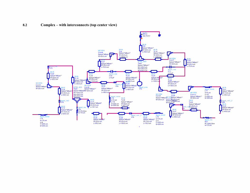
8.0 APPENDIX 8.1 Complex schematic – with interconnects (full view)
8.4 Complex – with interconnects (bottom right view)
MMIC Design Project Small Signal Amplifier
Thomas Neu 11/24/2005
Abstract This paper covers the design, results and conclusions of the MMIC final project. The goal for this project was to design a small signal amplifier (SSA) using a TriQuint MMIC process. The SSA is part of a larger system designed to receive and transmit signals from 5.15 to 5.85GHz. Our GaAS substrate was defined by the TriQuint MMIC process and the design was to fit on a 60 by 60 mil area. The amplifier was designed using the ‘Advanced Design System’ (ADS) software from Agilent which included the TriQuint elements library and was laid out in a 60 by 60 mil Anachip. The amplifier is intended to be used in the transmit as well as receive chain and will be used in a conjunction with other projects designed in this class.
Specification Goal Actual Result
Frequency:
Bandwidth:
Gain (small signal):
Gain Ripple:
Output IP3:
VSWR, 50Ohm:
Supply Voltage:
5.150 to 5.875 GHz
>800 MHz
>15 dB (16dB, goal)
+/- 0.5 dB
>20 dB
< 1.5:1 input & output
+/- 5V (+5 V goal)
4.7 to 6.1 GHz
1.4 GHz
17.7 dB
+/- 0.05 dB
~30 dB
<1.5:1 input & output
+ 5V
Introduction Circuit Description
The small signal amplifier is part of a larger system as shown below and therefore was designed to cover a very wide frequency range – from 5.1 to 5.9GHz. In order to cover this wide frequency range with a gain of at least 15dB, a two stage topology was chosen for this amplifier design. The first stage was designed for a gain of ~11dB while second has ~7dB with a feedback resistor to flatten out the gain. The two cascaded FET transistors are biased for class A operation and both FETs are the same size for design simplicity. The two transistors are configured as self biased to ease power supply requirements. Both stages draw about 30mA each from the supply which overall makes a fairly low power design considering a SSA gain of 17.5dB. Input and output matching networks are used to maximize the gain but also to get the best input and output match.
~VCO
Tune
5150 - 5350 MHz
10 dBm
or 5725 - 5875 MHz
Chip Set for the 5150 - 5350 MHz WLAN and5725 - 5875 MHz ISM Bands
LNA SS Amp
5150 - 5350
5725 - 5875MHz RF
15 dB 15 dB
PA-6 dBm
20 dBm SS Amp
13 dB 15 dBI/Q
Mod0, 2, 4, 6 dB
Transmit Single Element
-2 dB
90, 180-3 dB
5150 - 5350
5725 - 5875MHz RF
LNA SS Amp
15 dB 15 dB 90, 180-3 dB
Receive Array•••
1 of 4 Elements
4 W
AY
CO
MB
INER
~VCO
Tune
5150 - 5350 MHz
10 dBm
or 5725 - 5875 MHz
XIQMIX
X
Vector Mod
~~
I/QDeMod
~VCO
Tune
5150 - 5350 MHz
10 dBm
or 5725 - 5875 MHz
~VCO
Tune
5150 - 5350 MHz
10 dBm
or 5725 - 5875 MHz
Chip Set for the 5150 - 5350 MHz WLAN and5725 - 5875 MHz ISM Bands
LNA SS Amp
5150 - 5350
5725 - 5875MHz RF
15 dB 15 dB
PA-6 dBm
20 dBm SS Amp
13 dB 15 dBI/Q
Mod0, 2, 4, 6 dB
Transmit Single Element
-2 dB
90, 180-3 dB
5150 - 5350
5725 - 5875MHz RF
LNA SS Amp
15 dB 15 dB 90, 180-3 dB
Receive Array•••
1 of 4 Elements
4 W
AY
CO
MB
INER
~VCO
Tune
5150 - 5350 MHz
10 dBm
or 5725 - 5875 MHz
~VCO
Tune
5150 - 5350 MHz
10 dBm
or 5725 - 5875 MHz
XIQMIX
XXX
IQMIXXX
Vector Mod
~~~~
I/QDeMod
1. Design Approach 1.1 Transistor selection:
The small signal amplifier consists of two cascaded transistor stages and both stages use a 300um DFET transistor. Initially only one stage was considered, however the gain was fairly narrow band. A feedback resistor ‘flattens’ and widens the RF gain but also attenuates it significantly. Therefore a two stage approach was chosen where the first stage provides most of the gain while the second stage with feedback resistor turns the circuit into a wide band amplifier.
1.2 Biasing:
First the Idss (saturated drain source current) was determined at Vgs=0V using the FET tracer tool and it came out to about 68mA as shown in figure 4. For best linear output power, Ids should be about 55-60% of Idss, so roughly 36mA. Both transistors are configured as self biased transistors (resistor at FET source controls drain current) and for Ids of ~35mA, Vgs should be ~ -0.35V as shown in the simulation below. Bypass capacitors at the source resistors help controlling the gain a little more.
1.3 Matching Networks:
For optimum gain and VSWR, the input and output of the SSA are typically matched with a conjugate complex match to a 50 Ohm impedance. In this design, the input was tuned with a shunt and series inductor while the output was matched with a shunt capacitor and a series inductor. Another critical element in this design is the connection between first and second stage. A large capacitor is used as a DC block to separate the DC bias of 1st and 2nd stage and a series inductor matches the output of stage one to the input of stage 2.
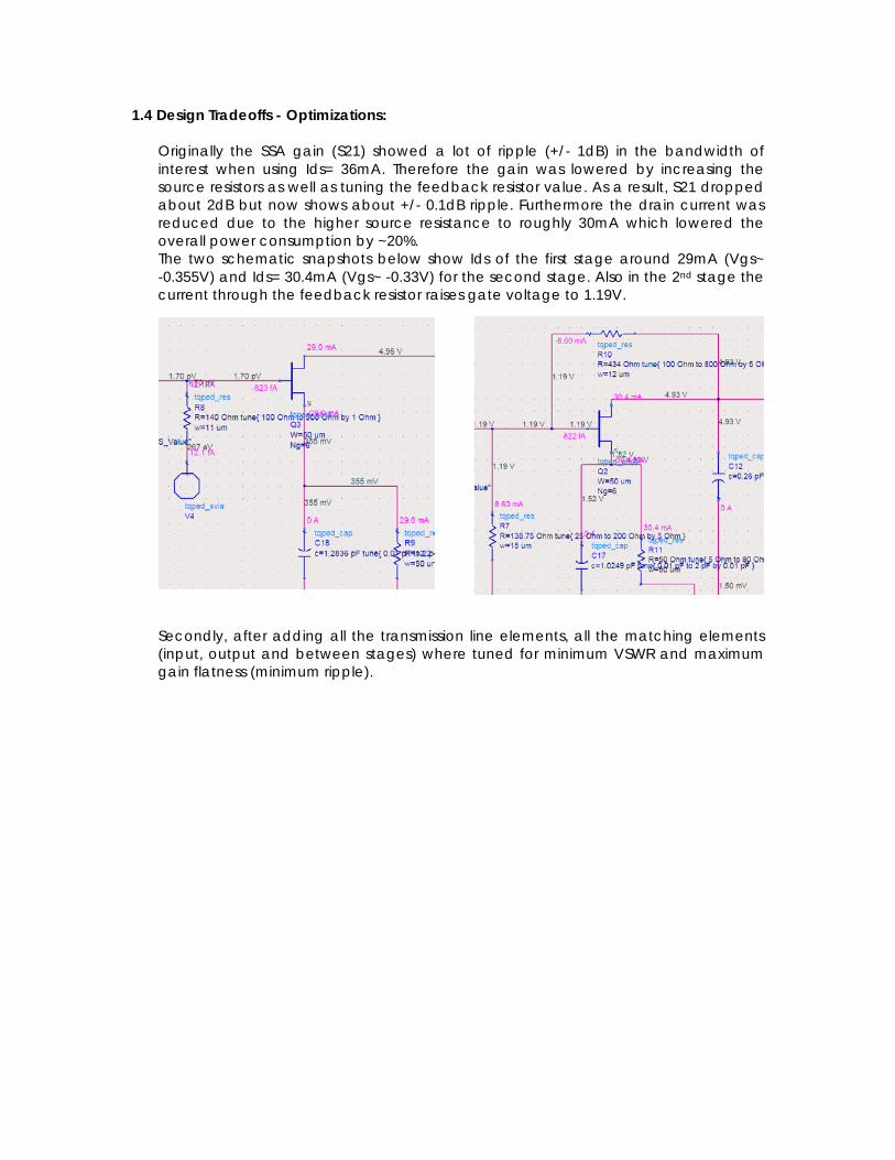
1.4 Design Tradeoffs - Optimizations: Originally the SSA gain (S21) showed a lot of ripple (+/- 1dB) in the bandwidth of interest when using Ids= 36mA. Therefore the gain was lowered by increasing the source resistors as well as tuning the feedback resistor value. As a result, S21 dropped about 2dB but now shows about +/- 0.1dB ripple. Furthermore the drain current was reduced due to the higher source resistance to roughly 30mA which lowered the overall power consumption by ~20%. The two schematic snapshots below show Ids of the first stage around 29mA (Vgs~ -0.355V) and Ids= 30.4mA (Vgs~ -0.33V) for the second stage. Also in the 2nd stage the current through the feedback resistor raises gate voltage to 1.19V.
Secondly, after adding all the transmission line elements, all the matching elements (input, output and between stages) where tuned for minimum VSWR and maximum gain flatness (minimum ripple).
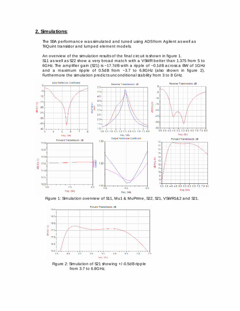
2. Simulations: The SSA performance was simulated and tuned using ADS from Agilent as well as TriQuint transistor and lumped element models. An overview of the simulation results of the final circuit is shown in figure 1. S11 as well as S22 show a very broad match with a VSWR better than 1.375 from 5 to 6GHz. The amplifier gain (S21) is ~17.7dB with a ripple of ~0.1dB across a BW of 1GHz and a maximum ripple of 0.5dB from ~3.7 to 6.8GHz (also shown in figure 2). Furthermore the simulation predicts unconditional stability from 3 to 8 GHz.
Figure 1: Simulation overview of S11, Mu1 & MuPrime, S22, S21, VSWR1&2 and S21.
Figure 2: Simulation of S21 showing +/-0.5dB ripple from 3.7 to 6.8GHz.
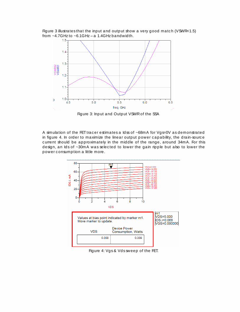
Figure 3 illustrates that the input and output show a very good match (VSWR<1.5) from ~4.7GHz to ~6.1GHz – a 1.4GHz bandwidth. A simulation of the FET tracer estimates a Idss of ~68mA for Vgs=0V as demonstrated in figure 4. In order to maximize the linear output power capability, the drain-source current should be approximately in the middle of the range, around 34mA. For this design, an Ids of ~30mA was selected to lower the gain ripple but also to lower the power consumption a little more.
Figure 3: Input and Output VSWR of the SSA
Figure 4: Vgs & Vds sweep of the FET.
At 5.5GHz input, the 1dB compression point is around -2dBm input power, at 5.0GHz it is around -2.5dBm input power as shown below.
The output IP3, measured at the 1dB compression point, is about 29.7dB at 5.0GHz and about 33.6dB at 5.5GHz as shown in the simulation plots below.
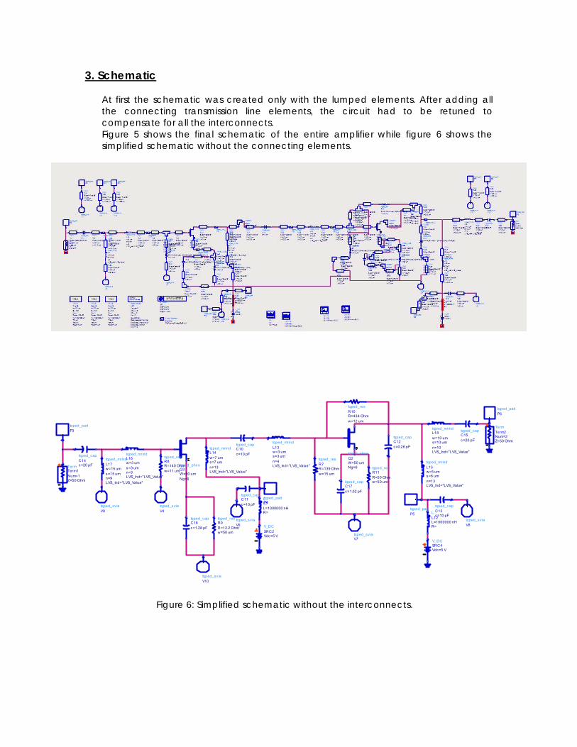
3. Schematic
At first the schematic was created only with the lumped elements. After adding all the connecting transmission line elements, the circuit had to be retuned to compensate for all the interconnects. Figure 5 shows the final schematic of the entire amplifier while figure 6 shows the simplified schematic without the connecting elements.
Figure 6: Simplified schematic without the interconnects.
tqped_resR9
w=50 umR=12.2 Ohm
tqped_phssQ3
Ng=6W=50 um
tqped_capC18c=1.28 pF
tqped_resR8
w=11 umR=140 Ohm
tqped_mrindL16
LVS_Ind="LVS_Value"n=3s=3 umw=3 um
tqped_sviaV4
tqped_mrindL17
LVS_Ind="LVS_Value"n=9s=15 umw=15 um
tqped_sviaV9
tqped_capC14c=20 pFTerm
Term1
Z=50 OhmNum=1
tqped_padP3
tqped_resR10
w=12 umR=434 Ohm
tqped_sv iaV7
tqped_sv iaV8
tqped_pad
P6
TermTerm2
Z=50 OhmNum=2
tqped_capC15c=20 pF
tqped_mrindL18
LVS_Ind="LVS_Value"n=10
s=10 umw=10 um
tqped_capC13c=10 pF
L
L12
R=L=1000000 nH
V_DCSRC4Vdc=5 V
tqped_padP5
tqped_mrindL15
LVS_Ind="LVS_Value"n=13
s=6 umw=5 um
tqped_capC12c=0.26 pF
tqped_resR11
w=50 umR=50 Ohm
tqped_capC17c=1.02 pF
tqped_resR7
w=15 umR=139 Ohm
tqped_mrind
L13
LVS_Ind="LVS_Value"n=4s=3 umw=3 um
tqped_capC10c=10 pF
tqped_mrindL14
LVS_Ind="LVS_Value"n=13s=7 umw=7 um
tqped_sviaV6
tqped_padP4LL3
R=L=1000000 nH
V_DCSRC2Vdc=5 V
tqped_capC11c=10 pF
tqped_sv iaV10
tqped_phssQ2
Ng=6W=50 um
4. Layout
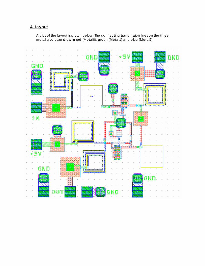
A plot of the layout is shown below. The connecting transmission lines on the three metal layers are show in red (Metal0), green (Metal1) and blue (Metal2).
5. Test Plan Design verification of the SSA requires measuring s-parameters (S11, S21, S22) as well as output IP3 and DC parameters (power consumption).
5.1 Test Equipment:
The following test equipment will be needed to characterize the SSA: - Agilent 8510 network analyzer - Cascade Model 43 wafer probe station with 2 RF probes and 4 DC needle probes - Synthesized signal generator up to 10GHz - Spectrum analyzer up to 10GHz - Simple DC power supply
5.2 Turn-On Procedure:
The SSA requires two 5V supplies – one for each transistor but the SSA can be powered by just one DC power supply. In order to protect the MMIC SSA, the current limit on the power supply should be set to 1.5 times the nominal DC current which is about 90mA ((30mA+29mA)x 1.5).
5.3 S-Parameter Measurements:
After calibrating the network analyzer, connect the DC and RF probes to the MMIC SSA as shown with the labels on layout. After setting the current limits on the DC power supply, S11, S21 and S22 can be measured with the VNA. The drain currents can be measured with a simple multimeter.
5.4 1dB Compression Point:
Since the frequency spectrum of interest is so wide (1GHz), the 1dB compression point measurement should be performed at three frequencies (5.0, 5.5 & 6.0GHz). The signal generator provides the input signal at the desired frequency to the SSA and the output power level can be recorded with the spectrum analyzer. The initial input power level should be relatively low, around -15dBm. The measured output power minus the provided input power level should equal the small signal gain (S21). By raising the input power level and subtracting the gain from the output power, the 1dB compression point can be determined. According to simulation the 1dB compression should ~ +2dBm input power.
5.5 Output IP3 Measurements:
For the IP3 measurement, two signal generators are the necessary. The input tones should be spaced ~10MHz (e.g. f1= 5.50GHz and f2= 5.51GHz). This should ensure that the amplitudes at the transistor input are identical since the attenuation should be the same for such close frequencies. The power levels for both input tones should be set to the same level as well.
The first measurement should be at a very low input power level, e.g. -15dBm. Using the spectrum analyzer, the output tone level as well as third order output (2*f2-f1) level need to be recorded. The delta between the third order products and the fundamental tones is the third order intercept (TOI) value. This measurement can be repeated two or three more times (e.g. -15dBm, -10dBm, -5dBm and 0dBm) and the TOI values recorded. The TOI values can plotted against input power and the intersection of TOI and Pout is the output IP3 point.
6 Summary and Conclusion
The small signal amplifier was designed and simulated using ADS from Agilent with TriQuint semiconductor DFET transistor and lumped element models. The simulation of the final schematic shows a gain of ~17.5dB with exceptionally good gain ripple (~ +/- 0.1dB) and very good input and output match (VSWR < 1.4). The amplifier itself promises fairly low power consumption with roughly only 60mA from a single +5V supply.
C-Band Vector Modulator and
I/Q Demodulator
Tom Beglin and Greg Eckenrode December 10, 2005
1
Abstract – This paper details a C-Band .5um pHEMT Vector Modulator and I/Q Demodulator with an I/Q frequency of 50 MHz. The design was simulated using Agilent’s Advanced Design Systems along with models supplied by TriQuint. The simulations predict the Vector Modulator to have a minimum insertion loss of ~5dB and the I/Q Demodulator has a conversion loss of ~3dB.
2
Table of Contents Introduction 3 Design Approach 4 Simulations 5 Schematics 8 Layout 10 Test Plan 11 Conclusion 12
3
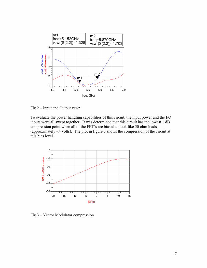
1. Introduction 1.1 Circuit Description – Vector Modulator The vector modulator design consists of a 90-degree hybrid to split the RF input into I/Q components, two attenuators to control the amplitude and sign of the I and Q components, and a combiner to sum the two signals. Because of the limited amount of space, the 90-degree hybrid was realized using a lumped element equivalent circuit. Reflective attenuators were designed using the same 90-degree hybrid along with two transistors biased as variable resistors by the I and Q inputs. The combiner is a simple lumped element Wilkinson design. 1.2 Circuit Description – I/Q Demodulator The I/Q Demodulator uses the same architecture except for the replacement of the variable resistors with diode connected FET’s. The RF and LO signals are fed into the two RF pads (they can be interchanged), and the 50 MHz I/Q outputs will vary in amplitude depending on the relative phase of the RF signal with respect to the LO signal. The diodes are driven on by the LO input, which was simulated at an input level of +12 dBm to the entire chip.
4
2. Design 2.1 Lumped Element 90 degree hybrid The 90 degree hybrids used in both circuits are a simple lumped element design optimized at a center frequency of 5.5 GHz. For this frequency, a distributed network was unrealizable in the given area. The ideal hybrid was converted to a lumped element circuit by replacing the quarter wavelength sections with equivalent low pass networks. 2.2 Wilkinson Divider Similarly to the 90 degree hybrid, the Wilkinson divider/combiner was realized with equivalent lumped elements at C-band due to size constraints. 2.3 Transistor Sizing for Vector Modulator For the Vector Modulator, the range of the variable resistors is the determining factor in the range of the reflective attenuators. Ideally, a perfect short and a perfect open would yield an attenuation range of +1 to -1. A large resistance is easy to obtain by putting a large enough negative bias on the gate of the FET. Creating a good short requires a larfe FET, but a large FET also adds parasitic capacitance that can skew the constellation of the vector modulator. A 105 um FET turned out to be a good compromise. With a gate bias of +.5 volts, the FET had a series resistance of about 10 ohms. The capacitance of the FET was negligible at the frequency of interest. Assuming I/Q inputs of -.7 to +.5 volts, our total range of resistance is approximately 10 to 250 ohms. 2.4 Diode Sizing for I/Q Demodulator For the I/Q Demodulator, we used diodes sized to be approximately 50 ohm loads. This was done to minimize the effects of the diodes on the 90 degree hybrid. With a 12 dBm input, the diodes should be operating near the threshold voltage, so the diodes were sized based on a bias of .7 volts. Diode connected FETs with a single finger of 50 um turned out to be about 50 ohms at this bias level. 2.5 Layout Design The layout of the 90 degree hybrid circuits was done to minimize the interaction of the two reflective attenuators and any possible cross-talk between the I and Q components. The 90 degree hybrids and the Wilkinson were then re-optimized to compensate for the interconnect within the individual components. The next step was to interconnect the hybrid circuits and Wilkinson and then add in the FETs. Another iteration of tuning was necessary to compensate for this lengthy interconnect. See figures 1 and 2.
5
3. Simulations 3.1 Vector Modulator The vector modulator was simulated with swept DC inputs for the I and Q signals. Careful considerations were made to ensure that this circuit would work at the specified 50 MHz as well. Figure 1 shows a polar plot of the output constellation with gate biases swept from -.7 to +.5 volts. As you can see, it has a usable range out to an amplitude of .3, or just over 5 dB of loss. This complies with the specified loss goal of no more than 7 dB. It should be noted that the output is highly nonlinear with respect to the I/Q voltages. It is assumed that this will be compensated by the back end of the system.
-0.4 -0.3 -0.2 -0.1 0.0 0.1 0.2 0.3 0.4-0.5 0.5
freq (5.500GHz to 5.500GHz)
S(2,1)
Fig 1 – Vector modulator output constellation Figure 2 shows the RF input and output vswr, both of which meet the spec of 2.5:1. The output vswr comes close, but does not meet the goal of 1.5:1 at the upper edge of the band. The I/Q input vswr is nearly perfect due to the 50 ohm shunt resistor at these inputs.
6
4.5 5.0 5.5 6.0 6.54.0 7.0
2
3
4
1
5
freq, GHz
vswr(S(2,2))
m1m2
m1freq=vswr(S(2,2))=1.328
5.152GHzm2freq=vswr(S(2,2))=1.703
5.879GHz
vswr(S(1,1))
RFin
dBm(vout[::,1])
Fig 2 – Input and Output vswr To evaluate the power handling capabilities of this circuit, the input power and the I/Q inputs were all swept together. It was determined that this circuit has the lowest 1 dB compression point when all of the FET’s are biased to look like 50 ohm loads (approximately -.4 volts). The plot in figure 3 shows the compression of the circuit at this bias level.
-15 -10 -5 0 5 10-20 15
-40
-30
-20
-10
-50
0
Fig 3 – Vector Modulator compression
7
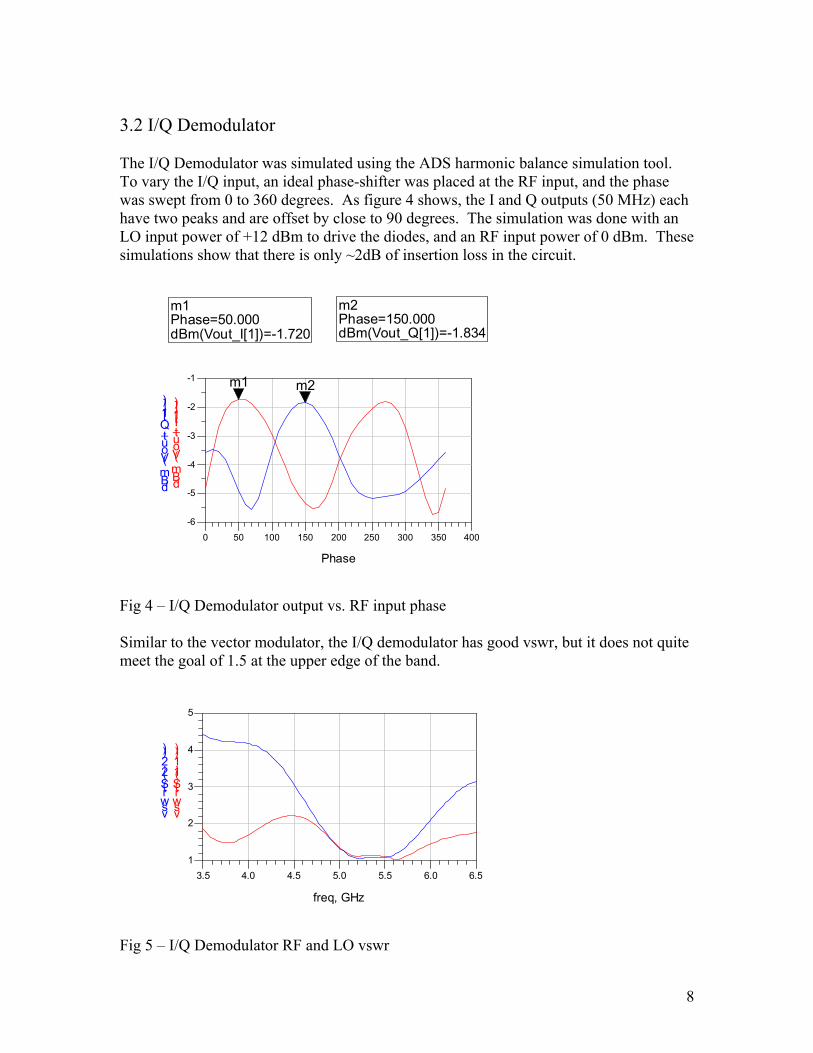
3.2 I/Q Demodulator The I/Q Demodulator was simulated using the ADS harmonic balance simulation tool. To vary the I/Q input, an ideal phase-shifter was placed at the RF input, and the phase was swept from 0 to 360 degrees. As figure 4 shows, the I and Q outputs (50 MHz) each have two peaks and are offset by close to 90 degrees. The simulation was done with an LO input power of +12 dBm to drive the diodes, and an RF input power of 0 dBm. These simulations show that there is only ~2dB of insertion loss in the circuit.
50 100 150 200 250 300 3500 400
-5
-4
-3
-2
-6
-1
Phase
m1
dBm(Vout_Q[1])
m2
m1Phase=dBm(Vout_I[1])=-1.720
50.000m2Phase=dBm(Vout_Q[1])=-1.834
150.000
dBm(Vout_I[1])
vswr(S(1,1))
Fig 4 – I/Q Demodulator output vs. RF input phase Similar to the vector modulator, the I/Q demodulator has good vswr, but it does not quite meet the goal of 1.5 at the upper edge of the band.
4.0 4.5 5.0 5.5 6.03.5 6.5
2
3
4
1
5
freq, GHz
vswr(S(2,2))
Fig 5 – I/Q Demodulator RF and LO vswr
8
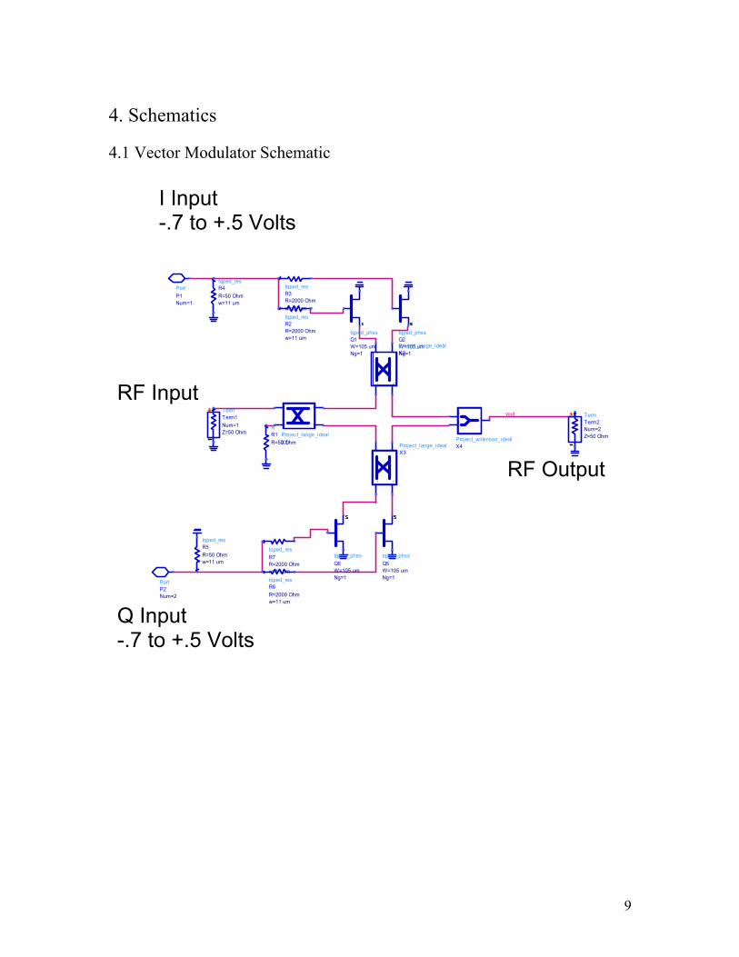
4. Schematics 4.1 Vector Modulator Schematic
I Input -.7 to +.5 Volts
vout
tqped_phss
Q5
Ng=1W=105 um
tqped_phss
Q6
Ng=1W=105 um
tqped_res
R7
w=11 umR=2000 Ohm
tqped_resR6
w=11 umR=2000 Ohm
PortP2Num=2
tqped_resR5
w=11 umR=50 Ohm
tqped_resR4
w=11 umR=50 Ohm
Port
P1Num=1
tqped_resR3
w=11 um
R=2000 Ohm
tqped_resR2
w=11 umR=2000 Ohm tqped_phss
Q2
Ng=1W=105 um
tqped_phssQ1
Ng=1W=105 um
RR1
R=50 Ohm
TermTerm2
Z=50 OhmNum=2
Project_lange_ideal
X1
4
1
3
2
Project_lange_idealX2
41
32
Project_lange_idealX3
41
32
Project_wilkinson_idealX4
2
1
3TermTerm1
Z=50 OhmNum=1
RF Input
RF Output
Q Input -.7 to +.5 Volts
9
4.2 I/Q Demodulator Schematic
vout
tqped_capC2c=5 pF
tqped_capC1c=5 pF
PortP3Num=3
tqped_phssQ7
Ng=1W=50 um
tqped_phssQ8
Ng=1W=50 um
PortP2Num=2
tqped_phssQ6
Ng=1W=50 um
tqped_phssQ5
Ng=1W=50 um
RR1R=50 Ohm
TermTerm2
Z=50 OhmNum=2
Project_lange_idealX1
4
1
3
2
Project_lange_idealX2
41
32
Project_lange_idealX341
32
Project_wilkinson_idealX4
2
1
3TermTerm1
Z=50 OhmNum=1
I Output
RF Input
LO Input
Q Output
10
5. Layout 5.1 Vector Modulator Layout
I Input (DC)
RF Output (GSG)
RF Input (GSG)
Q Input (DC)
5.2 I/Q Demodulator Layout
I Output
RF Input (GSG)
LO Input (GSG)
Q Output
11
6. Test Plan 6.1 Test Equipment
• Agilent 8510 Network Analyzer • DC power supply • Two signal generators with phase-locking capability • Spectrum anlayzer
6.2 Test Procedure 6.2.1 Vector Modulator Test Procedure The Vector Modulator can be easily tested by measuring the RF input to RF output on a network analyzer. First, a calibration from 5 to 6 GHz should be performed on the network analyzer. Measurements of the device should then be taken with each of the bias settings listed in the table below. After the data has been taken, single frequency points can be plotted on a polar chart across bias settings to verify a good constellation of RF output magnitudes and phases.
6.2.1 I/Q Demodulator Test Procedure The I/Q Demodulator will require two RF sources phase locked together with an offset of 50 MHz. These signals should be input into the RF and LO GSG pads on the device, and the I/Q outputs should be observed on a spectrum analyzer. The input power should be 0 dBm on the RF input and 12 dBm on the LO input. To test that the I and Q components are being separated out of the RF signal, a relative phase shift will have to be inserted between the RF source and the device. This can be realized by lengthening the cable between the RF source and the device in small increments (possibly with several RF connectors in a row). The relative changes in phase of this cable should be measured on a network analyzer prior to beginning this test. The amplitude of the 50 MHz I/Q outputs should then be measured and plotted versus the relative phase shift (see simulation plot in section 3.2). 7. Conclusion The design of a C-Band Vector Modulator and I/Q Demodulator have been described. The simulations were performed using ADS and they showed that the vector modulator will have an insertion loss of ~5 dB while the I/Q demodulator will have a conversion loss of ~2 dB. The designs will be fabricated at TriQuint using the .5um pHEMT process. 8. References 1. Penn, John E. “A Balanced Ka-Band Vector Modulator MMIC.” Microwave Journal, June 2005.
EE525.787 – Microwave Monolithic Integrated Circuit (MMIC)Engineering and Applied Science Programs for Professionals
Instructors: John Penn & Dr. Michel Reece
C-Band Low Noise Amplifier (LNA)
Microwave Monolithic Integrated Circuit (MMIC)
Designer: Wilart Banks December 12, 2005
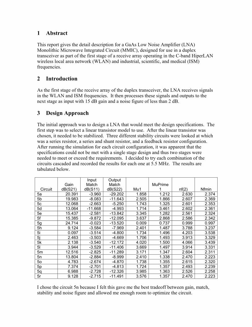
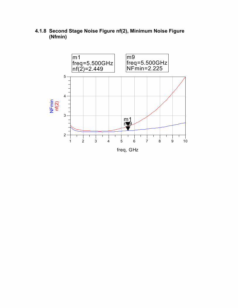
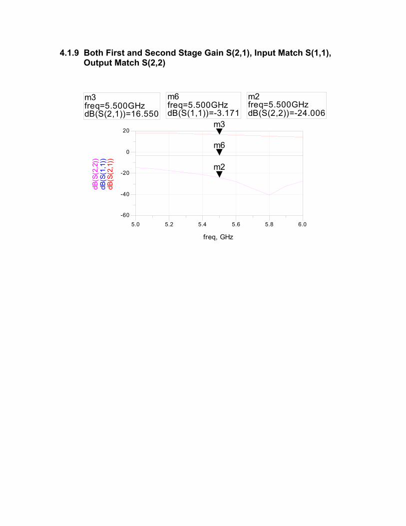
1 Abstract This report gives the detail description for a GaAs Low Noise Amplifier (LNA) Monolithic Microwave Integrated Circuit (MMIC), designed for use in a duplex transceiver as part of the first stage of a receive array operating in the C-band HiperLAN wireless local area network (WLAN) and industrial, scientific, and medical (ISM) frequencies. 2 Introduction As the first stage of the receive array of the duplex transceiver, the LNA receives signals in the WLAN and ISM frequencies. It then processes these signals and outputs to the next stage as input with 15 dB gain and a noise figure of less than 2 dB. 3 Design Approach The initial approach was to design a LNA that would meet the design specifications. The first step was to select a linear transistor model to use. After the linear transistor was chosen, it needed to be stabilized. Three different stability circuits were looked at which was a series resistor, a series and shunt resistor, and a feedback resistor configuration. After running the simulation for each circuit configuration, it was apparent that the specifications could not be met with a single stage design and thus two stages were needed to meet or exceed the requirements. I decided to try each combination of the circuits cascaded and recorded the results for each one at 5.5 MHz. The results are tabulated below.
Circuit Gain
dB(S21)
Input Match
dB(S11)
Output Match
dB(S22) Mu1 MuPrime
1 nf(2) Nfmin 5a 20.391 -3.960 -29.202 1.858 1.212 2.630 2.3745b 19.983 -8.083 -11.643 2.505 1.866 2.607 2.3695c 12.068 -2.663 -5.250 1.743 1.325 2.601 2.3535d 13.064 -11.668 -4.993 1.714 3.461 2.602 2.3615e 15.437 -2.581 -13.842 3.345 1.282 2.561 2.3245f 15.385 -9.872 -12.095 3.637 2.868 2.586 2.3425g 24.714 -0.023 -13.520 0.009 0.737 0.999 0.9975h 9.124 -3.584 -7.969 2.401 1.487 3.788 3.2375i 0.097 -3.514 -4.800 1.734 1.496 4.203 3.5385j 2.463 -3.503 -4.669 1.706 1.493 3.913 3.3295k 2.138 -3.540 -12.172 4.020 1.500 4.066 3.4395l 3.944 -3.529 -11.406 3.669 1.497 3.914 3.3315m 12.516 -2.825 -11.289 3.171 1.347 2.604 2.3115n 13.804 -2.884 -8.999 2.410 1.338 2.470 2.2235o 4.783 -2.674 -4.870 1.738 1.355 2.615 2.3205p 7.374 -2.701 -4.813 1.724 1.357 2.493 2.2395q 6.988 -2.728 -12.326 3.985 1.363 2.526 2.2585r 9.128 -2.715 -11.491 3.576 1.357 2.470 2.223 I chose the circuit 5n because I felt this gave me the best tradeoff between gain, match, stability and noise figure and allowed me enough room to optimize the circuit.
After the linear circuit was stable and it met the requirements, I replaced the linear model with the non-linear TriQuint model and tuned the circuit to get the final results. 3.1 Specifications vs. Goals For the design, the following specifications to design to were also my goals to achieve. Specifications Goals
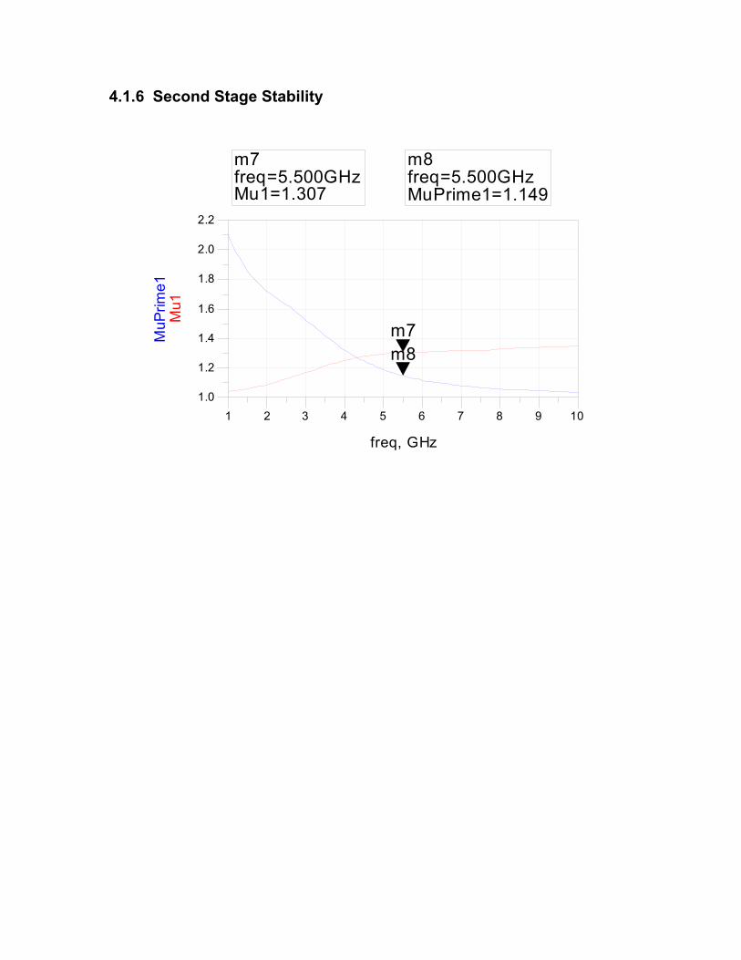
Size 60 x 60 mil ANACHIP 60 x 60 mil ANACHIP 3.2 Tradeoffs The LNA design has many tradeoffs associated with it such as balancing gain, stability, match and noise figure. This particular design has its major tradeoff between gain and noise figure. Care was taken to not over compensate for one by sacrificing the other. By tuning the output matching circuit of the second stage, I was able to achieve my goal of 15 dB gain while also achieving a noise figure less than 2 dB. 3.3 Circuit Description The LNA is a two-stage design with two transistors cascaded using the output from the first stage as the input to the second stage. Each stage was designed to fulfill different purposes. The first stage for low noise and the second stage for output match and gain bandwidth. Both stages of the LNA utilize a TriQuint 6x50 0.5µm PHEMT biased at 3V of drain voltage and 15 mA drain current. The first stage of the LNA utilizes a series and shunt resistor for stability. Because this particular design has very low noise, it is used in the design as the first stage since this stage sets the overall noise figure. The second stage of the LNA utilizes a feedback resistor for stability. This design is used in the second stage to improve output match and increase the gain bandwidth of the amplifier. 4 Simulations
4.1 Linear
4.1.1 First Stage Gain S(2,1), Input Match S(1,1), Output Match S(2,2)
tqped_capC3c=0.65 pF tune 0.65 pF to 1.95 pF by 0.1 pF
tqped_resR7
w=12.5 um notune 6.25 um to 18.75 um by 1.25 um R=10 Ohm notune 5 Ohm to 1000 Ohm by 1 Ohm
tqped_resR8
w=11 umR=30 Ohm notune 5 Ohm to 300 Ohm by 1 Ohm
tqped_resR2
w=11 um notune 5.5 um to 16.5 um by 1.1 um R=475 Ohm notune 10 Ohm to 500 Ohm by 5 Ohm
tqped_capC11c=20 pF
TermTerm2
Z=50 OhmNum=2
tqped_sviaV4
tqped_capC7c=20 pF
V_DCSRC2Vdc=VGS
V_DCSRC1Vdc=VDS
tqped_sviaV5
tqped_capC8c=20 pF
TermTerm1
Z=50 OhmNum=1
tqped_capC10c=20 pF
tqped_mrindL3
LVS_Ind="LVS_Value"n=12s=10 umw=10 um I_Probe
IDS
tqped_sviaV1
tqped_capC2c=241 fF
tqped_mrindL8
LVS_Ind="LVS_Value"n=12s=10 umw=10 um
tqped_capC12c=20 pF
tqped_mrindL4
LVS_Ind="LVS_Value"n=12s=10 umw=10 um
tqped_capC9c=20 pF
tqped_mrindL9
LVS_Ind="LVS_Value"n=12s=10 umw=10 um
tqped_sviaV3
tqped_mrindL5
LVS_Ind="LVS_Value"n=12s=10 umw=10 um
I_ProbeIDS1tqped_phss
Q2
Ng=6W=50 um
5.2 RF Schematic with interconnect
tqped_resR5
w=5 umR=2000 Ohm
MLINTL6
L=220 umW=10 umSubst="MSub1"
V_DCSRC2Vdc=VGS
LL12
R=L=1000000 nH
tqped_sviaV4
tqped_capC7c=20 pF
MLINTL7
L=150 umW=10 umSubst="MSub1"
tqped_padP4
MLINTL9
L=300 umW=10 umSubst="MSub1"
MLINTL8
L=160 umW=10 umSubst="MSub1"
tqped_resR6
w=5 umR=2000 Ohm
MLINTL10
L=105 umW=10 umSubst="MSub1"
tqped_resR2
w=11 um notune 5.5 um to 16.5 um by 1.1 um R=475 Ohm notune 10 Ohm to 500 Ohm by 5 Ohm
tqped_capC9c=20 pF
MLINTL11
L=190 umW=10 umSubst="MSub1"
MLINTL20
L=140 umW=10 umSubst="MSub1"
tqped_mrindL4
LVS_Ind="LVS_Value"n=12s=10 umw=10 um
MLINTL19
L=250 umW=10 umSubst="MSub1"
tqped_capC12c=20 pF
tqped_padP3
MLINTL31
L=240 umW=10 umSubst="MSub1"
V_DCSRC1Vdc=VDS
LL11
R=L=1000000 nH
tqped_resR8
w=11 umR=40 Ohm notune 5 Ohm to 300 Ohm by 5 Ohm
tqped_sviaV3
MLINTL15
L=210 umW=10 umSubst="MSub1"
tqped_mrindL5
LVS_Ind="LVS_Value"n=12s=10 umw=10 um
MLINTL5
L=210.0 umW=10 umSubst="MSub1"
MLINTL4
L=380 umW=10 umSubst="MSub1"
tqped_mrindL3
LVS_Ind="LVS_Value"l2=150 um notune 100 um to 300 um by 10 um l1=150 um notune 100 um to 300 um by 10 um n=12s=10 umw=10 um
TermTerm1
Z=50 OhmNum=1
MLINTL2
L=80 umW=10 umSubst="MSub1"
tqped_capC10c=20 pF
MLINTL3
L=110.0 umW=10 umSubst="MSub1"
tqped_padP1
MLINTL28
L=320 umW=10 umSubst="MSub1"
tqped_mrindL10
LVS_Ind="LVS_Value"n=12s=10 umw=10 um
MLINTL25
L=330 umW=10 umSubst="MSub1"
tqped_capC8c=20 pF
tqped_sviaV5
MLINTL30
L=65 umW=10 umSubst="MSub1"
MLINTL29
L=320 umW=10 umSubst="MSub1"
I_ProbeIDS1
tqped_mrindL9
LVS_Ind="LVS_Value"n=12s=10 umw=10 um
MLINTL13
L=460 umW=10 umSubst="MSub1"
MLINTL12
L=140 umW=10 umSubst="MSub1"
MLINTL14
L=140 umW=10 umSubst="MSub1"
TermTerm2
Z=50 OhmNum=2
MLINTL16
L=170 umW=10 umSubst="MSub1"
tqped_capC11c=20 pF
tqped_padP2
MLINTL17
L=140 umW=10 umSubst="MSub1"
tqped_capC3c=0.45 pF tune 0.2 pF to 1.95 pF by 0.1 pF
tqped_phssQ1
Ng=6W=50 um
MLINTL24
L=50 umW=10 umSubst="MSub1"
tqped_sviaV10
MLINTL26
L=50 umW=10 umSubst="MSub1"
MLINTL21
L=90 umW=10 umSubst="MSub1"
tqped_mrindL8
LVS_Ind="LVS_Value"n=12s=10 umw=10 um
tqped_sviaV1
MLINTL22
L=70 umW=10 umSubst="MSub1"
tqped_capC2c=241 fF
MLINTL23
L=70 umW=10 umSubst="MSub1"
tqped_resR7
w=12.5 um notune 6.25 um to 18.75 um by 1.25 um R=15.2 Ohm notune 5 Ohm to 1000 Ohm by 1 Ohm
I_ProbeIDS
MLINTL27
L=170 umW=10 umSubst="MSub1"
tqped_sviaV11
MLINTL18
L=460 umW=10 umSubst="MSub1"
tqped_phssQ2
Ng=6W=50 um
6 Layout Plot
7 Test Plan Verifying the design of the LNA MMIC will require the measurement of such parameters as the noise figure and S-parameters. 7.1 Test Equipment The use of the following test equipement is required to measerrue the performance of the LNA. Spectrum Analyzer Network Analyzer 5 volt DC Power Supply Power Meter
7.2 Turn On Procedure Extreme caution should be used so as to prevent an excess of drain voltage and current from entering the circuit. The required voltage is +3 V DC and the required current is 30 mA for the LNA. Setting the correct limits on the DC supply is a must. 7.3 RF Measurements The test equipment should be calibrated prior to performing any test on the LNA MMIC. Calibrate the analyzer from 1 – 10 GHz. The noise figure meter should be calibrated as well. 7.4 S-Parameters Measurements After calibration of the test equipment, probes should be connected to the LNA and measurement of current and S11, S12, S21, S22 can be made and recorded. 7.5 Noise Figure Measurements After calibrating the noise figure meter, position the probes on the VD pad and IN input pads and record the noise figure over the band of frequencies. 8 Summary & Conclusion This report describes the design of a C-Band LNA MMIC designed to operate at 5.5 MHz using the TriQuint process. The design was simulated using Agilent Advanced Design System. The simulated model produced an LNA with gain of 15 dB or greater in the required frequency band and noise figure of less than 2 dB on a 300mm ANACHIP footprint. This designed was produced as part of the MMIC Design course taught at Johns Hopkins University of the Fall 2005 semester.
Phase Shifter Final Report
Drew Wilson JHU 525.787 MMIC Design
December 12, 2005
Abstract A MMIC 2-bit phase shifter for the 5.8 GHz ISM band was designed using the Triquint Semiconductor TQPED process. Simulation and layout were performed with Agilent ADS. The phase shifter is one component of a duplex transceiver being built as a class exercise at Johns Hopkins University. Introduction
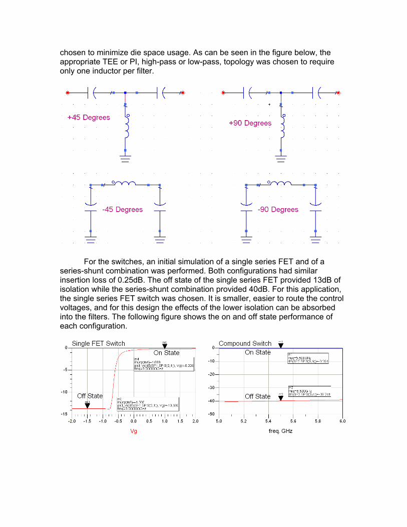
A phase shifter is a two-port microwave device whose phase response changes according to an external input. The phase shifter designed here accepts logical inputs to select from four phase states. This will be used in the signal path of each element of an antenna array. By changing the phase of the signals, the antenna array beam can be steered without physically moving the antenna. The specifications for this phase shifter are as follows: Frequency: 5150 to 5875 MHz Bandwidth: > 800 MHz Insertion Loss: < 4 dB (3dB Goal) Insertion Loss Balance: +/- 1 dB Phase Shift: Steps of 45 (Goal), 90, 180 Degrees VSWR to 50 Ohms: <1.5:1 on Input and Output Supply Voltage: +/- 5 Volts Control: TTL (Goal) or 0/-5 Volt Size: 60 by 60 mil Design Approach A straightforward topology was chosen to implement the phase shifter. The topology is a parallel combination of two phase filters in series with a second parallel combination of two phase filters. One filter from each parallel combination is selected with FET switches. The first parallel combination is of filters with +45 degree and –45 degree phase shifts. The second parallel combination is of filters with +90 degree and –90 degree phase shifts. By selecting either +45 or –45 degrees and +90 or-90 degrees, the following relative phase shifts can be realized: First Filter Second Filter Absolute Shift Relative Shift (Subtract 45) +45 +90 +135 +90 -45 +90 +45 0 +45 -90 -45 -90 -45 -90 -135 180 Once the general topology is chosen, the four individual filters and the switches had to be designed. For the filters, lumped elements were used to generate the required phase shift. The +90 and –90 degree filters implemented as lumped element quarter wavelength transformers. Copies of these were tuned to generate the +45 and –45 degree filters. The topology of each filter was
chosen to minimize die space usage. As can be seen in the figure below, the appropriate TEE or PI, high-pass or low-pass, topology was chosen to require only one inductor per filter.
For the switches, an initial simulation of a single series FET and of a series-shunt combination was performed. Both configurations had similar insertion loss of 0.25dB. The off state of the single series FET provided 13dB of isolation while the series-shunt combination provided 40dB. For this application, the single series FET switch was chosen. It is smaller, easier to route the control voltages, and for this design the effects of the lower isolation can be absorbed into the filters. The following figure shows the on and off state performance of each configuration.
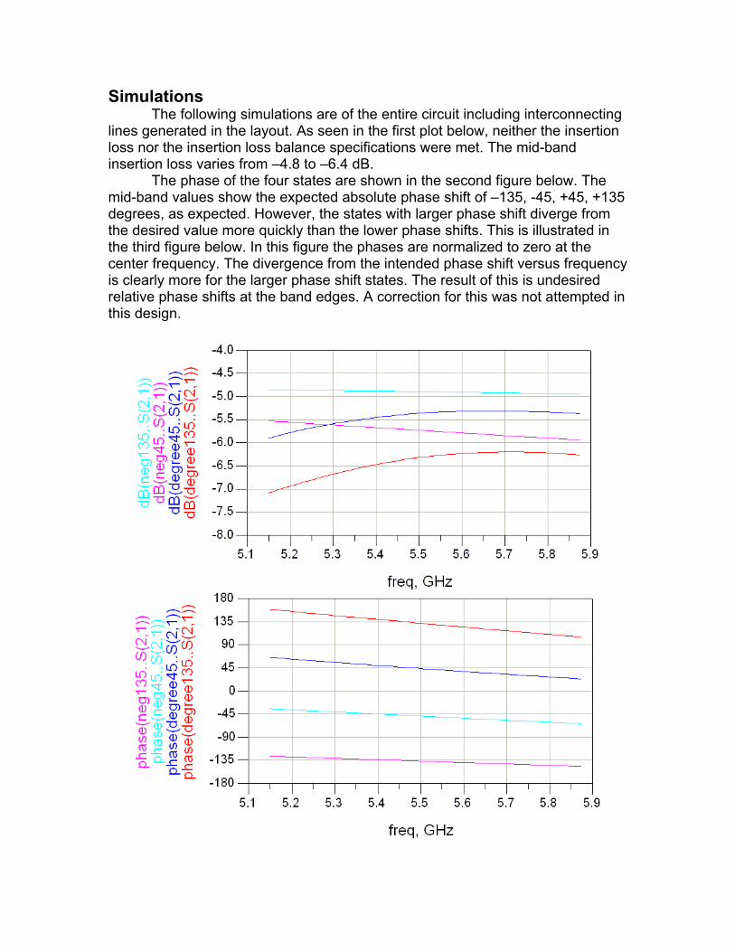
Simulations The following simulations are of the entire circuit including interconnecting lines generated in the layout. As seen in the first plot below, neither the insertion loss nor the insertion loss balance specifications were met. The mid-band insertion loss varies from –4.8 to –6.4 dB. The phase of the four states are shown in the second figure below. The mid-band values show the expected absolute phase shift of –135, -45, +45, +135 degrees, as expected. However, the states with larger phase shift diverge from the desired value more quickly than the lower phase shifts. This is illustrated in the third figure below. In this figure the phases are normalized to zero at the center frequency. The divergence from the intended phase shift versus frequency is clearly more for the larger phase shift states. The result of this is undesired relative phase shifts at the band edges. A correction for this was not attempted in this design.
The input and output impedance match specification is VSWR of 1.5:1 on input and output. This corresponds to a return loss of –14dB. A plot of input and output port return loss is below. The impedance match specification was met on the input, but not the output. During the design only the input impedance match was monitored.
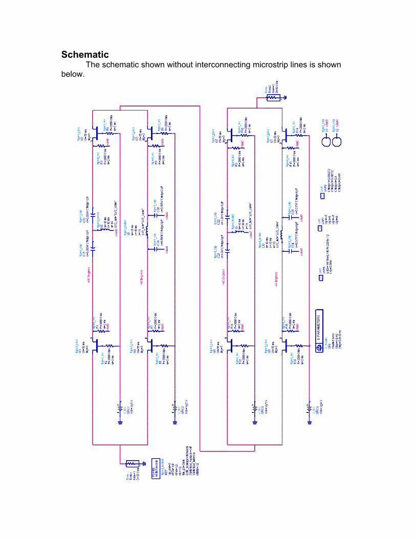
Schematic The schematic shown without interconnecting microstrip lines is shown below.
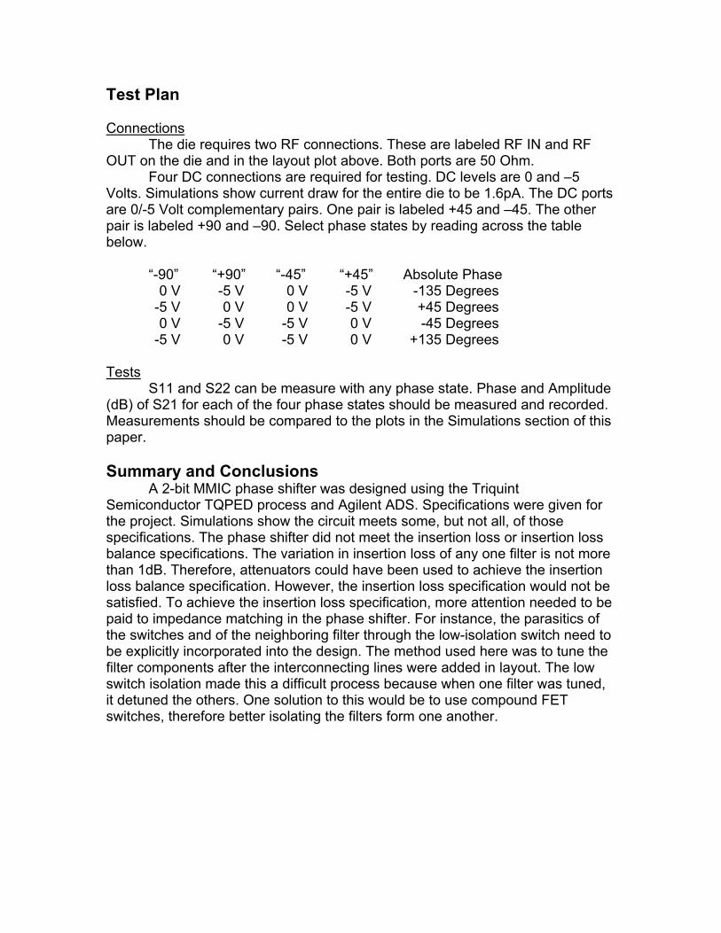
Layout Plot A plot of the layout follows. In this plot, the two RF ports are labeled RF IN and RF OUT. Each of these has ground-signal-ground pads on opposite sides of the die for testing on a wafer probe station. There are four DC connections to be made to the die. These are toward to four corners of the chip and spaced away from the RF connections. This is to simplify needle probe connections. These four ports are labeled –90, -45, +90, +45.
Test Plan Connections The die requires two RF connections. These are labeled RF IN and RF OUT on the die and in the layout plot above. Both ports are 50 Ohm. Four DC connections are required for testing. DC levels are 0 and –5 Volts. Simulations show current draw for the entire die to be 1.6pA. The DC ports are 0/-5 Volt complementary pairs. One pair is labeled +45 and –45. The other pair is labeled +90 and –90. Select phase states by reading across the table below. “-90” “+90” “-45” “+45” Absolute Phase 0 V -5 V 0 V -5 V -135 Degrees -5 V 0 V 0 V -5 V +45 Degrees 0 V -5 V -5 V 0 V -45 Degrees -5 V 0 V -5 V 0 V +135 Degrees Tests S11 and S22 can be measure with any phase state. Phase and Amplitude (dB) of S21 for each of the four phase states should be measured and recorded. Measurements should be compared to the plots in the Simulations section of this paper.
Summary and Conclusions A 2-bit MMIC phase shifter was designed using the Triquint Semiconductor TQPED process and Agilent ADS. Specifications were given for the project. Simulations show the circuit meets some, but not all, of those specifications. The phase shifter did not meet the insertion loss or insertion loss balance specifications. The variation in insertion loss of any one filter is not more than 1dB. Therefore, attenuators could have been used to achieve the insertion loss balance specification. However, the insertion loss specification would not be satisfied. To achieve the insertion loss specification, more attention needed to be paid to impedance matching in the phase shifter. For instance, the parasitics of the switches and of the neighboring filter through the low-isolation switch need to be explicitly incorporated into the design. The method used here was to tune the filter components after the interconnecting lines were added in layout. The low switch isolation made this a difficult process because when one filter was tuned, it detuned the others. One solution to this would be to use compound FET switches, therefore better isolating the filters form one another.
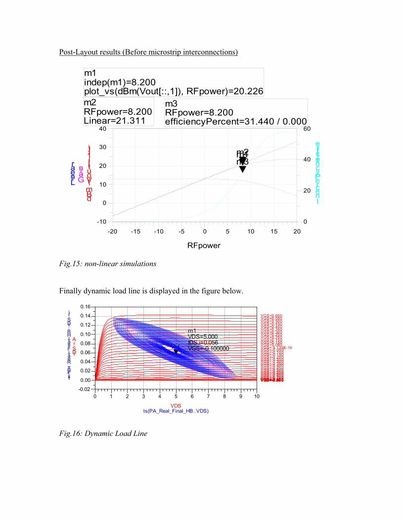
Finally dynamic load line is displayed in the figure below.
1 2 3 4 5 6 7 8 90 10
0.00
0.02
0.04
0.06
0.08
0.10
0.12
0.14
-0.02
0.16
m1
ts(PA_Real_Final_HB..VDS)
ts(PA_Real_Final_HB..IDS.i)
m1VDS=IDS.i=0.056VGS=-0.100000
5.000
Fig.16: Dynamic Load Line
Layout
Test plan
Ground-Signal-Ground (G-S-G) pads are required in order to perform RF measurements
using the HP 8510 Vector Network Analyzer and Cascade probe station. These pads are
shown in the Final Layout figure above and are labeled RFIN and RFOUT for the RF
input and output respectively. RF probes will come in from the left and right of the chip
for input and output, respectively as shown in the layout.
For the DC bias, pads are put on top and bottom of the chip for VDS and VGS bias
respectively. 5 and –0.1 volts supplies will be connected to the VDS and VGS pads
respectfully.
The VNA 8510 will be used to measure all linear measurements while the spectrum
analyzer will be used to perform non linear measurements.
Below is a list of all equipment to be used. Test Equipment:
• Agilent 8510 VNA (45 MHz to 26 GHz)
• Cascade Model 43 wafer probe station with up to 4 RF probes & 4 DC needle probes
• Synthesized signal generators to 26 GHz
• Spectrum analyzer to 18 GHz
Conclusion The design of PA for the C-Band Transceiver was successfully done. All the goals were
not met but the most important ones were met, namely Power Added Efficiency and
Output power of, 31.4 % and 20.226 dBm respectively. The input VSWR of 1.2 was
achieved meeting the requirement of <1.5. The specifications that were not met were not
far off, hence the settling of the final design. One of these specifications was the small
signal gain. It was supposed to be 13 dB across the band but the design yielded 12.4 dB
gain across the band. A difference of 0.6 dB was not that critical to make the decision to
do a 2 stage design. Output VSWR achieved was 2.37 but this was expected to be off due
to the nature of the output matching design. The design and layout were both done using
ADS circuit simulator. This exercise was very informative and enabled tremendous
growth towards becoming RF MMIC designer.
References
1. Steven C. Cripps,”RF Power Amplifiers for Wireless Communications,” Artech House, 1999, chapters 3, 5, 8.
2. Penn, John and Reece, Michel. Class Handouts. JHU/APL. 2005.
John Hopkins University Part Time Engineering Program for Professionals
Making Microwaves MMIC VCO Design Via Impedance Matching
Edward Heine
Abstract This final design report for the John Hopkins University Fall 2005 MMIC Design course details the design of an MMIC VCO. The MMIC VCO is designed on the TRI-Quint TQPED process. The VCO design goals are a tuning range of 5150 to 5350 MHz or 5725 to 5875 MHZ, maximum 5 volt supply, 0 to 0.6 volts for control, lowest phase noise and an output power grater than +7 dBm. The emphasis of this repost is on making the VCO cover both tuning ranges and choosing the varactor. An on chip Emode PHEMT device is used for the varactor. Microwave Office is used for the simulation and layout.
1 of 17
1. Introduction
The design project for the Fall 2005 MMIC Design class at The Johns Hopkins
University is a duplex transceiver employing a receive array for the C-band HiperLAN
wireless local area network (WLAN) and industrial, scientific, and medical (ISM)
frequencies. For transmission, a direct vector modulator is used to transmit data onto the
carrier. For downlink, an I/Q down converter is used to derive modulated data. The
frequency carrier consists of a VCO. The VCO operates from 5150 to 5350 MHz, or
~VCO
Tune
5150 - 5350 MHz
10 dBm
or 5725 - 5875 MHz
Chip Set for the 5150 - 5350 MHz WLAN and5725 - 5875 MHz ISM Bands
LNA SS Amp
5150 - 5350
5725 - 5875MHz RF
15 dB 15 dB
PA-6 dBm
20 dBm SS Amp
13 dB 15 dBI/Q
Mod0, 2, 4, 6 dB
Transmit Single Element
-2 dB
90, 180-3 dB
5150 - 5350
5725 - 5875MHz RF
LNA SS Amp
15 dB 15 dB 90, 180-3 dB
Receive Array•••
1 of 4 Elements
4 W
AY
CO
MB
INER
~VCO
Tune
5150 - 5350 MHz
10 dBm
or 5725 - 5875 MHz
XIQMIX
X
Vector Mod
~~
I/QDeMod
~VCO
Tune
5150 - 5350 MHz
10 dBm
or 5725 - 5875 MHz
~VCO
Tune
5150 - 5350 MHz
10 dBm
or 5725 - 5875 MHz
Chip Set for the 5150 - 5350 MHz WLAN and5725 - 5875 MHz ISM Bands
LNA SS Amp
5150 - 5350
5725 - 5875MHz RF
15 dB 15 dB
PA-6 dBm
20 dBm SS Amp
13 dB 15 dBI/Q
Mod0, 2, 4, 6 dB
Transmit Single Element
-2 dB
90, 180-3 dB
5150 - 5350
5725 - 5875MHz RF
LNA SS Amp
15 dB 15 dB 90, 180-3 dB
Receive Array•••
1 of 4 Elements
4 W
AY
CO
MB
INER
~VCO
Tune
5150 - 5350 MHz
10 dBm
or 5725 - 5875 MHz
~VCO
Tune
5150 - 5350 MHz
10 dBm
or 5725 - 5875 MHz
XIQMIX
XXX
IQMIXXX
Vector Mod
~~~~
I/QDeMod
Figure 1 Project block diagram
2 of 17
5725 to 5875 MHz, to cover the WLAN and ISM frequencies. A phase shifter chip
implements a 2 bit phase for the receive array. Transmit level control is implemented
with the MMIC attenuator chip. Each element of the receive chain array consists of an
LNA and a driver amplifier in cascade, followed by a phase shifter. The transmit path
employs a driver amplifier feeding a 100 milliwatt power amplifier. Nine unique MMIC
designs make up the S-band transceiver. Each design is to be contained on a 60 mil
square die in the TQPED process. The proposed block diagram is shown in Figure 1.
The emphasis of this report is on the VCO design and test procedure. The VCO is
designed on the Tri-Quint TQPED process. Microwave Office is used for the simulation
and layout. Utilizing the device’s small signal parameters, the oscillator is designed
using the reflection method. A non-linear simulation was ran to check the output power
and phase noise. No optimization is done based on the non-linear simulation. The drain
and source of an Emode PHEMT is grounded to make varactor using the TQPED
process. The design chronicles the design process. Using the available 60x60 mil die
area the circuit is laid out. A test procedure is detail in the test section and the expected
results are summarized in the conclusion section
2. Design
The VCO is designed using the reflection method (often called negative impedance
method) of oscillator design. The essence of this method is to reduce a non-linear
three terminal device to a linear two port equivalent circuit and match the two ports
appropriately. In this instance the PHEMT (3 terminal device) gate is taken as one
port and the drain is taken as the other port. It is accepted that if the device is
oscillating in one port, it must also be oscillating in the other port. The output can be
taken at either the drain or the gate. To achieve maximum output power the drain is
chosen for the output. This leaves the gate for the resonant circuit. Now that the
function of each port is identified, like most other microwave designs, the linearized
circuit is now an impedance matching task. Unlike other microwave designs,
choosing the proper terminating impedance is not a strait forward task and requires
iteration. The details of the VCO impedance matching are chronicled below.
3 of 17
The operating point was chosen to meet the power requirement (Vd=3.0 volt, Id=15
mA) and reduce the noise.
2.1. Examine FET to determine topology
The gain and stability factor of the non-linear PHEMT model is plotted in Figure
2. The PHEMT’s measured s-parameter data is also plotted to increase
confidence in the non-linear model. The non-linear and linear model agree up to
Figure 2 Gain and stability of PHEMT. Gain and st
~14 GHz. This is sufficient for this design.
ability shown for linear and no-linear
he device has a lot of gain at the lower frequencies and is conditionally stable.
ust
model.
T
Compensation must be added to the device to reduce the lower frequency gain
and stabilize the device outside the desired oscillation frequency range. This m
Now that the device is compensated and biased the gate matching requirement can
be determined using the 2 port circuit response. Figure 3 will be used extensively
to determine the proper gate matching requirement.
5 of 17
ain’s
p1: FREQ = 5.8 Stability =
Reflection
0.2
2.0
This circle is the mapping of the gate impedance onto the drain impedance plane. For example plot a real impedance on this plane (blue chart) and the distance from the plotted point to the center of the of the drain's Smith Chart will be the drreflection coefficient.
0.2
The green x is the gate impedance (2.67 nH) that maximizes the drain's reflection coefficient. The magnitude of the reflectionis 3.745 or the precipice ofu1 from the last section.
The maximum possible drain reflection coefficient. By Foster’s reactance theorem we know the reflection coefficient
Any impedance in this region will cause oscillation. The goal is to chose the gate impedance that causes the maximum Reflection coefficient at the drain. The inverse of mu is the maximum reflection coefficient.
Swp Max5.8GHz
0.5
0.5 1.0
Gate stability circle i.e. mapping of gate Into drain.
Figure 4 Plot showing the drain’s reflection coefficent.
Figure 3 is a plot of the drain’s (output) reflection coefficient at 5.8 GHz. The
heavy black circle is the boundary of the unit Smith chart. The pinkish circle is a
stability circle mapping the gate’s impedance. Choosing a gate impedance in the
overlapping region can cause the drain reflection coefficient to be greater than
unity i.e. oscillate. The problem is choosing the best gate impedance. A
reasonable criterion is to select the impedance which maximizes the drain’s
reflection coefficient. Recall we know the maximum drain reflection from the
last step, 1/u1=3.745. A convenient way to determine the gate impedance is to
map all possible gate impedance’s onto the drain’s reflection coefficient’s plane.
The blue circle is this mapping (very nice feature of Microwave Office). The
green X on the mapping (blue circle) represents the maximum drain reflection
coefficient. This is verified by replacing the gate with the requisite gate
impedance (2.67 nH) and plotting the drain reflection coefficient. As expected
6 of 17
the drain reflection coefficient is 3.7. The gate impedance should be 2.67 nH for
a maximum drain reflection coefficient.
2.3. Designing the varactor
The source and drain of a PHEMT is grounded to a make varactor. The critical
parameters are the available tuning range and the Q. Two varactor configurations
were considered, a 6 finger device or a 10 finger device. The equivalent circuit
model for each device is determined and used for comparison.
The equivalent circuit model and the matching between the model and the actual
device are shown in Figure 4. Notice the model accurately matches the device
over .1 to 20 GHz. This indicates the model is good.
Table 1 shows the capacitance and ESR for a 6 finger and a 10 finger device over
the tuning voltage. The 10 finger device has a lower ESR. The 10 finger device
will be used in this design.
7 of 17
Varactor test circuitModel
Swp 20G
CAID=CC=1e4
1.0
PORP=Z=50
0.6
S(1,1Emode Configured as
0.8
2.0TQPED_TOM
ID=EHSS_W=5NG=1 0.4RE
ID=RR=2000
2 3.0S(2,2Linear 1
5.04.0
30.2
DCVID=VV=0 10.0
10.00.
43.0
0.8
0.2
2.0
5.0
1.0
4.0
0.60
Varactor equivalent -10.0
CAID=CC=0.507
REID=RR=2.58
PORP=Z=50 -0.2
-5.0-4.0
-3.0CAID=CC=0.0152 -0.4
-2.RE
ID=RR=2040
-0. -
0.8
Swp Min0.1G
-1.0
Figure 4 Varactor model
Table 1 Table of varactor capacitance and ESR for a 6 finger and 10 finger device.
Vtune 6 Finger
(pF)
6 Finger
(ohms)
10 finger
(pF)
10 finger
(ohms)
0 0.249 6.9 0.507 2.58
0.2 0.381 5.8 0.78 2.58
0.4 0.7 4.9 1.29 2.58
0.6 1.32 4.3 2.3 2.25
8 of 17
2.4. Design the gate matching network.
Now that the varactor model and the desired gate match has been determined, the
gate matching network can be designed. The gate circuit is shown in Figure 5.
The ideal gate match was an inductor. The limited Q of the inductor and varactor
make realizing this match over a wide frequency range difficult.
The load circuit should present the correct phase rotation and loading as
determined in Figure 3. The correct phase is 180 degrees i.e. rotating the
reflection coefficient to resonance. The resonance type can be read off the Smith
chart. The resonance is series. Note the gate match from the previous step is used
to determine actual matching values. A rule of thumb is to make the loading
impedance one third the negative impedance.
9 of 17
Add length of line to the drain, making the reflection 180 deg at oscillation. The line length is 76 degrees. The impedance seen looking into the drain is -22 ohms. So the load should be less than 22/3 or <~7 ohms.
Figure 6. Drain reflection with gate and source match. The output is and ideal match.
The ideal match was converted to a 2 element match at a single frequency. This
simple matching circuit may not be sufficient, because the reactance slope has not
been matched. At this point in the design the circuit was laid out and design rule
checked. A more complex output matching circuit was designed. The more
complex matching circuit had trouble fitting into the available space. Due to time
requirements the decision was made to go with the simple output matching circuit
that had passed the design rule check. The circuit passed design rule checking
and no further iterations were preformed.
10 of 17
2.6. The VCO response
The completed matched circuit is shown in
CAP_LVS_SHORTID=C2C=4 pF
DCVSID=V1V=3 V
INDID=L1L=Ldrain nH
INDID=L3L=Lgate nH
RES_LVS_OPENID=rg1R=Rgate Ohm
CAP_LVS_SHORTID=C4C=csource pF
I_METERID=AMP1
RES_LVS_OPENID=rg2R=rsource Ohm
Fo Fn. . .
SWPFRQID=FSWP1Values=5.8e9
1
2
3
TQPED_TOM3ID=PHSS_1W=50NG=6
V_PROBEID=VP1
V_PROBEID=VP2
CAPID=C3C=Cmo pF
INDID=L5L=Lmo nH
CAPID=C1C=4 pF
INDID=L2L=3.75 nH
DCVSID=V3V=Vtune V
RESID=R1R=2000 Ohm
1
2
3
TQPED_TOM3ID=EHSS_1W=50NG=10
PORTP=1Z=50 Ohm
Figure 7. The VCO
The output reflection coefficient for vtune=1 and 0 volt is shown in Figure 9 and
Figure 8. The VCO should operate over the full range. The reflection coefficent
is small at the lower end on the range and may not oscillate.