EE318 Electronic Design Lab Report, EE Dept, IIT Bombay, April 2005
FAN REGULATOR WITH PROGRAMMABLE PROFILE AND
VOLTAGE REGULATION
Group No. B2
Shagun Dusad (02007035) <[email protected]>
Anshul Khandelwal (02007016) <[email protected]>
Anosh Raj (02007002) <[email protected]>
1
Contents
1 Problem Statement 3
1.1 Motivation 1
2 Design Approach 4 2.1 Power supply voltage detection circuit 5
2.2 Zero Crossing Detector 7
2.3 The Microcontroller - TRIAC Circuit 8
2.4 The TRIAC - Load Circuit 8
2.5 User Interface Circuit 10
3 Circuit diagram 11
4 Test results, plots, Interpretations 13
5 Component Description 19
6 Cost Analysis 20
5 Conclusion and Suggestions for further improvements 21
REFERENCES 22
APPENDIX 23
2
List of Figures
Fig 2.1: State Machine for Key Detection
Fig 2.2 : State Machine for the User Interface
Fig 2.3 : A general connection between a load and the TRIAC (BTA06C [5])
Fig 3.1 : Schematic Diagram of the Circuit
Fig 3.2 : The complete Circuit Diagram
Fig 4.1 : a)Mains Supply b)Voltage across TRIAC c)Voltage waveform across Inductive
load for speed level 2.
Fig 4.2 : a)Mains Supply b)Voltage across TRIAC c)Voltage waveform across Inductive
load for speed level 2.
Fig 4.3: a)Mains Supply b)Voltage across TRIAC c)Voltage waveform across Inductive
load for speed level 8.
Fig 4.4 : Voltage waveform of different magnitudes with frequency constant
Fig 4.5 : Voltage waveform across load for different magnitudes as shown above.
Fig 4.6 : Two waveforms of different frequency with same voltage level
Fig 4.7 : The voltage waveform across the load
Fig 4.8 : a)Voltage waveform across the low voltage side of the transformer b)Voltage
waveform across the full-bridge rectifier output c)Voltage waveform across the capacitor
following the rectifier
3
Problem statement
The objective of our design project is to build a fan/light regulator which follows a user
programmable linear profile, provides regulation against input power supply voltage
variation and also takes into account the frequency variation of the power supply.
1.1 Motivation
In normal regulators, the device operation level (fan-speed light-intensity) is set by the
user and does not vary according to the later conditions. Also it does not adjust itself to
voltage and frequency variations after it is set to the present level. User comfort is largely
increased if the regulator can be programmed to follow a particular profile and also adjust
itself against power variations. For example for a person back from work would require
more fan speed initially and during the dawn hours would like to decrease the speed. In
normal fan regulators the speed would be same as the speed set before going to sleep and
also if the voltage level rises during the morning hours, it would lead to high speed than
required and causes user discomfort. Same case also applies to gradual waning or waxing
of light intensity or Air Conditioners.
So in our regulator we propose to take in a profile from the user in the initially in terms of
speed variation required by him and the time interval over which he requires the speed
variation. We then use ac regulation controlled by a microprocessor to follow the user
defined profile independent of input voltage and frequency of power supply.
In our project we will assume the profile to be linear, so we would require the initial
speed, final speed and time duration from the user. The user input will have five buttons -
device selection toggle, parameter selection toggle, increase selected parameter value,
decrease selected parameter value and accept profile.
4
Design approach
The speed (or intensity) of the fan (or light) is varied using AC voltage regulation based
on TRIAC. The firing angle pulses fed to the TRAIC decides the rms AC voltage.
Depending on power supply voltage and the input frequency, the microcontroller is
programmed to generate pulses to the gate of TRIAC to get the required rms AC voltage
for the particular point on the profile. The profile parameters which are the initial speed,
final speed and the time duration of the profile are set by user using two switches
provided. The value specification of the three parameters has been discretized to 0-9
levels. In case of speeds, the level 9 corresponds to α pulse being close to zero (to provide
maximum speed of the fan) whereas the level 0 corresponds to α pulse being equal to
eighty percent of the half power cycle (to protect the fan from damage due to very low
voltage). One switch is provided for to toggle between the three parameters (the
particular selected parameter is displayed using LEDs) and finally to indicate the profile
is to be accepted and the other switch is change the value of the particular parameter (the
values 0-9 are displayed on a 7 segment display). Once the user sets the three parameters
and presses the final accept switch, the microcontroller starts on the new profile. The
microcontroller scans for the user inputs and
Before the profile is set as soon as the power is switched on, the microcontroller fires
angles to provide the medium speed which would be comfortable to the user. After the
profile has elapsed, the microcontroller is programmed to continue at the final speed until
a new profile is fed. For powering the microcontroller and other components and also for
the measurement of the power supply voltage, the power supply is stepped down to lower
voltage (in our case using a transformer 230V/9V), rectified using a full-bridge diode
rectifier followed by a low pass filter which provides an almost constant dc voltage
directly proportional to the rms power supply voltage. This dc voltage (analog signal) is
read using an ADC and the microcontroller receives the digital value on which
calculations for the firing angle are based. Zero crossing detector is used to signal the
microcontroller the zero crossings of power supply whereas the internal timer in the
microcontroller is used to count time period of the half power supply cycle (time period
5
between two zero crossings). The present half cycle firing angle is based on the values of
voltage and frequency measured in the previous half cycle (this assumption allows us to
operate in real time).
When key-press is detected for the first time, after a time delay we again check for the
debouncing of the key (20 milliseconds). Once it is reasserted after this delay, we
consider the key press to be confirmed. Instead of continuous polling, we check for the
key press only at the end of each half cycle. As the time period of the power supply is
around 20 ms, it is used as a natural timer to check for the debouncing (we wait for two
half cycles). As the maximum α value is 80 % (as fan is considered for the purpose of the
regulation), there is enough time for processing at the end. But further action based on
the key detection is deferred until key release is confirmed (again we check after 20ms
for debouncing). The following state machine shows the key detection scheme and also
the two states which have been added so that we can use the power supply cycle as a
timer for debouncing check. For the period from the start of zero crossing and 80% of the
half cycle frequency is measured and alpha pulses are fired. In the next 20% of the time
user interface part runs, ADC part gives the current value of the voltage and calculation
of the α occurs. We assumed linear profile and linear variation of the voltage with α and
linear variation of speed with voltage.
6
Fig 2.1: State Machine for Key Detection
The above state machine is implemented for both toggle/accept key and increment key at
the end of each half cycle. One more state machine is implemented for the whole user
interface. Initially the state machine starts from state S0 in which the speed is set to be at
medium level and the microcontroller awaits for the first toggle/accept press. On a
toggle/accept key press, it moves to state S1 where every time increment key is pressed
the value of initial speed is moved in a cyclic order between 0-9 but it remains in S1.
Further, if toggle/accept key is pressed it moves to S2 where the value of final speed is
changed and finally in S3 the value of time duration is set. On the toggle/accept key in S3
implies that the new profile has been fed and the microcontroller starts on the new profile
from the next half cycle. The following state machine shows user interface
implementation.
7
Fig 2.2 : State Machine for the User Interface
2.1 Power supply voltage detection circuit
The low voltage side of the step down transformer (230V/9V) is connected to the full-
bridge diode rectifier circuit and the high voltage side is connected to the power supply.
The action of the full-bridge diode rectifier is to provide rectified full wave (ac to dc
conversion) which is taken across a low pass filter consisting of a capacitor and resistor
in parallel. The voltage across the capacitor is almost constant and has been used for two
purposes, one for power to the rest of the circuit and the other for voltage measurement as
an input to ADC. The first objective is achieved by a voltage regulator 7805 [8] which
provides a constant 5V supply. A single channel 8-bit ADC has been used for the voltage
measurement. Its voltage span has been adjusted to 1.9V-3.9V by providing a constant
1.9V to the analog ground and Vref/2. A zener diode was used for this purpose in
RESERVE BIAS MODE with a 5V voltage to its cathode through a resistor and its anode
connected to the ground. The clock is internally generated with CLK R connected to a
resistor and a capacitor to the ground and the voltage across the capacitor and ground is
8
fed to CLK IN. The CS (chip select) and RD are asserted by connecting them to ground
thereby providing continuous mode of operation. The write is asserted by a signal from
the microcontroller through P1.7 pin. After the conversion is completed, the ADC
interrupts the microcontroller through P2.7 pin. The digital values from are connected to
port 3 with LSB connected to P3.0 and the MSB connected to P3.7 and the other bits in
the same increasing order.
2.2 Zero Crossing Detector
The two ends of the low voltage side of the step down transformer are further connected
to resistor potential dividers. The voltage across the two legs of the resistor potential
divider are connected the inverting and non-inverting terminals of op-amp in LM324 [6].
The output pin of the LM324 [6] is connected to P1.6 of the microcontroller.
2.3 The Microcontroller - TRIAC Circuit
As the microcontroller can only sink small amount of current [3] ( less than four TTL
inputs) as an output buffer, we can’t connect it directly to the gate of the TRIAC. The SL
100 is a power transistor which takes in a large current from the microcontroller and a
PNP transistor (BC557 [9]) is used a buffer between the microcontroller and the NPN
transistor (SL 100). The output from P1.5 is connected to the base of a PNP transistor
(BC557 [9]) through a resistor, whose collector is grounded . Its emitter is connected to
the bases of a NPN transistor (SL100), which is also connected to the Vcc through a
resistance. The collector of NPN transistor is directly connected to the Vcc and the emitter
is grounded through a resistance. Their emitters are further connected to the Gates of the
TRIACs (BTA06 600C [5]).
9
2.4 The TRIAC - Load Circuit
Fig 2.3 A general connection between a load and the TRIAC (BTA06C [5])
The α pulses from the TRIAC driving circuit are connected to the pin 1 (the anode of the
photodiode) of the opto-coupler MOC 3020 [10] and the cathode is connected to the
ground of the electronic circuit. On the pulses, the photodiodes radiates and drives the
TRIAC inside MOC 3020 [10]. In this part the pulses are in optical form hence providing
the optical isolation between the TRIAC load circuit and the electronic circuit. The DAC
of the opto-coupler further drives the TRIAC with the load connected across it. As the
load is inductive (fan) and the TRIAC is non-sensitive, an additional resistor capacitor
network is used for the connection between MOC 3020 [10] and TRIAC. The MOC 3020
[10] drives the gate of the TRIAC while the load is connected in between a power supply
terminal and A2 terminal of the TRIAC and the other power supply terminal and A1 are
shorted. It is not necessary to connect the neutral and live in a specific way as an opto-
coupler has been used.
Minimum holding current must be maintained in order to keep a TRIAC
conducting. A TRIAC operates in the same way as the SCR, however, it operates in both
the forward and reverse direction. Major considerations, when specifying a TRIAC, are:
a) Forward & Reverse break-over voltage
b) Maximum current
c) Minimum holding current
d) Gate Voltage and gate current trigger requirements
e) Switching speed
10
2.5 User Interface Circuit
User interface consists of two switches (S1, S2), three LEDs (L1, L2, L3) and one seven
segment display. The microcontroller ports can sink a current less than four TTL inputs
when used as an input buffer and the total current that can be sinked in the
microcontroller is limited to 80mA to a port. So we designed the resistor values to
achieve a value less than 80mA assuming all seven segments (value 8) in the seven
segment display and one of the LEDs are on switched on at the same time. As the
microcontroller can only sink the current the cathodes of the LEDs (L1 ,L2, and L3) and
the seven segment display (a, b, c, d, e, f and g) is connected to the microcontroller (P1.0,
P1.1, P1.2, P2.0, P2.1,.......,P2.7 respectively), while the anodes are connected to the Vcc
with resistors to control the amount of current flowing through each LED. One end of
switches (S1 and S2) are connected to the ground and the other end is connected to Vcc
through a resistor where this end of the switch is connected to the microcontroller pins
P1.3 and P1.4. As soon the switch is pressed, the value of the pin connected to ground
and when the switch is released, the value of the pin is pulled up to the Vcc through the
resistor. They serve as inputs to the microcontroller.
11
Circuit diagram
The schematic diagram of the circuit consists of the following main blocks:
User Interface
Microcontroller
Zero Crossing detector
Diode and ADC circuit
TRIAC circuit
Fig 3.1 : Schematic Diagram of the Circuit
The detailed complete circuit diagram is on the next page Fig 3.2
12
Fig 3.2 : The complete Circuit Diagram
13
Test results, plots, Interpretations
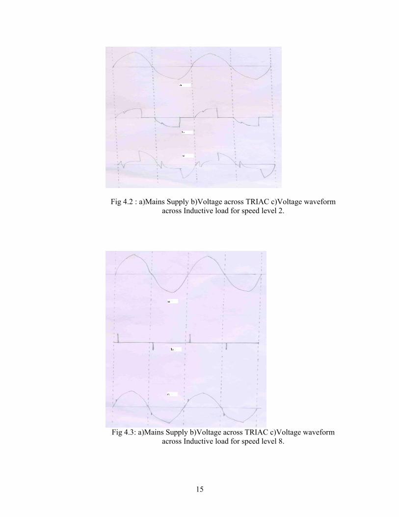
The voltage waveforms for three different speed levels - 2, 5 and 8 are shown below. It
can be observed from the wave forms as the speed level increases the firing angle is
delayed (increases towards 180) and the rms AC voltage decreases.
Fig 4.1 : a)Mains Supply b)Voltage across TRIAC c)Voltage waveform
across Inductive load for speed level 2.
14
Fig 4.2 : a)Mains Supply b)Voltage across TRIAC c)Voltage waveform across Inductive load for speed level 2.
Fig 4.3: a)Mains Supply b)Voltage across TRIAC c)Voltage waveform
across Inductive load for speed level 8.
15
For the purpose of demonstration of the voltage regulation, an autotransformer was used
to vary the input power supply to the fan regulator. Below three different voltage
waveforms with varying rms AC voltage are shown. It can be observed from the
waveforms as the voltage increases, the firing angle is delayed for the same speed level
so that the rms AC voltage remains constant
Fig 4.4 : Voltage waveform of different magnitudes with frequency constant
Fig 4.5 : Voltage waveform across load for different magnitudes as shown above.
16
For the purpose of demonstration of the frequency dependence of the firing angle,
frequency generator was used to vary the frequency of the input wave form. Below two
different voltage waveforms are shown with different frequencies but same voltage level.
It can be observed that as the frequency is decreased (dashed waveform), the firing angle
has been proportionally displaced.
Fig 4.6 : Two waveforms of different frequency with same voltage level
Fig 4.7 : The voltage waveform across the load
17
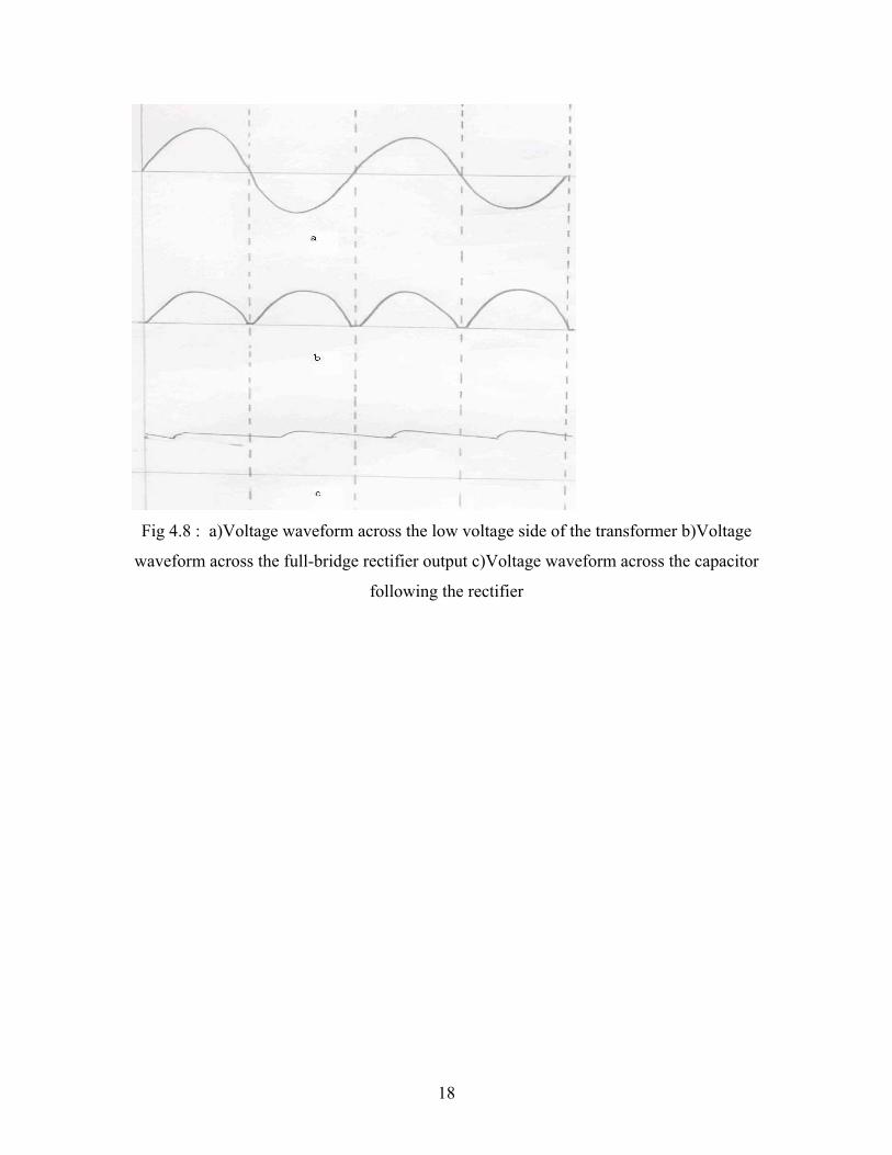
Fig 4.8 : a)Voltage waveform across the low voltage side of the transformer b)Voltage
waveform across the full-bridge rectifier output c)Voltage waveform across the capacitor
following the rectifier
18
Component Description
1. Microcontroller: AT89c52 [2]
The AT89c52 [2] is a low-power, high-performance CMOS 8-bit microcomputer with 8K
bytes of Flash programmable and erasable read only memory (PEROM), 256 bytes of
RAM, 32 I/O lines (four ports of 8 bits each – Port 0, Port 1, Port 2, Port 3), three 16-bit
timer/counters, a six-vector two-level interrupt architecture, a full-duplex serial port, on-
chip oscillator, and clock circuitry. Port 0 is an 8 bit open drain bi-directional I/O port.
Each pin as output port can sink 8 TTL inputs. Port 1, Port 2 and Port 3 are 8 bit bi-
directional I/O port with internal pull-ups and their output buffers can sink 4 TTL inputs.
Absolute Maximum Ratings
Maximum Operating Voltage: 6.6 V, DC Output Current: 15.0 mA, Voltage on any pin
with respect to Ground: -1.0V to 7.0V
2. LM324 [6]: Low Power Quad Operational Amplifiers
Features: Wide Power Supply Range, Single Supply: 3V to 32V, Dual supplies: + 1.5V to
+ 16V, Large Voltage Gain 100dB, Supply Voltage: 32V, Input Voltage: -0.3V to 32V
3. ADC0804 [4]:
It is a CMOS 8-bit successive approximation A/D converter that uses a differential
potentiometric ladder—similar to the 256R products.
Features: Resolution 8 bits, Total error ± 1/2 LSB, Access time 135 ns, Conversion time
100 µs, Differential analog voltage inputs (zero adjust not required), On-chip clock
generator, 0V to 5V analog input voltage range with single 5V supply
Operates with an adjusted voltage reference which allows encoding any smaller analog
voltage span to the full 8 bits of resolution.
19
COST ANALYSIS
Component Chip Number Cost/piece Quantity Total
CostVoltage Regulator LM7805 8.00 1 8.00
Microcontroller AT89c52 65.00 1 65.00
ADC ADC0804 55.00 1 55.00
Diodes IN4007 1.00 4 4.00
Op-amp LM324 20.00 1 20.00
LED - 1.00 3 3.00
TRIAC BTA 06 600C 15.00 1 15.00
Optocoupler moc3020 18.00 1 18.00
Transformer - 30.00 1 30.00
Zener Diode - 1.00 1 1.00
7 segment display LT542 20.00 1 20.00
NPN Transistor SL100 5.00 1 5.00
PNP Transistor BC 557 2.00 1 2.00
Crystal(12 MHz) - 20.00 1 20.00
Button Switches - 1.00 2 2.00
Resistor +
Capacitors
- 10.00 - 10.00
Total Cost 278.00
20
Conclusion and Suggestions for further improvements
The final product costs around Rs. 278 (excluding the cost of PCB and cabinet) and so
can be useful in replacing the traditional voltage regulator which costs around Rs. 250
where the power is wasted during the operation so achieving net profit in that respect as
well.
A watchdog timer can be included in the final product which will take care of the slow
initial voltages during start. It will start the regulator (the microprocessor program) after
some fixed elapsed time if found to be in an idle state.
21
References
[1] A. S. Sedra, K. C. Smith, “Microelectronic Circuits”, Fourth edition, 1982,
Oxford University Press (2003)
[2] K. J. Ayala, “8051 Microcontroller, Architecture, Programming & Applications”,
Penram International Publishing (India)
[3] Atmel Corporation, www.atmel.com/dyn/resources/prod_documents/doc0313.pdf
[4] National Semiconductor, http://cache.national.com/ds/DC/ADC0804.pdf
[5] ST Microelectronics, http://www.st.com/stonline/books/pdf/docs/2936.pdf
[6] National Semiconductor, http://cache.national.com/ds/LM/LM124.pdf
[7] Fairchild Semiconductorhttp://www.fairchildsemi.com/ds/1N/1N4003.pdf#page=1
[8] Fairchild Semiconductor, http://www.fairchildsemi.com/ds/KA%2FKA7805.pdf
[9] Fairchild Semiconductor, http://www.fairchildsemi.com/ds/BC/BC557.pdf
[10] Fairchild Semiconductor, http://www.fairchildsemi.com/ds/MO/MOC3020-M.pdf
22
APPENDIX
User Manual This device is used for setting a user profile for fan regulation and then operating
according to the profile set up by the user. It works independent of the frequency of the
electric supply and also of the voltage of the supply (to a limit of 35-45 volts on either
side of the nominal voltage i.e., 230 V). By pressing a set of buttons on the device can be
operated. The buttons have to be pressed in steps, to go about any of the desired tasks.
One end of the fan goes to the LINE of the power supply, while the other goes to the pin
A2 of the TRIAC. In all, 2 buttons on the device look after all the desired tasks,
associated with the fan.
The device can be used to select initial level of speed, final level of speed and the time
duration for the change to occur via a linear profile. The device has three LED’s showing
what is being selected at the moment. The following table illustrates it.
Selection Number of levels Indicators
Initial level of Speed 0 to 9 Red LED
Final level of Speed 0 to 9 Yellow LED
Time Interval 1 to 9 Blue LED
There are two button switches which works as follows:
BUTTON 1: For selecting the next item. These can be classified as follows
o Starting the user interface
o Initial level of speed
o Final level of speed
o Time duration
BUTTON 2: For incrementing the quantity selected. It starts incrementing from the last
last stored value of that quantity. That is, the device has memory.
23