University of Nebraska - Lincoln University of Nebraska - Lincoln DigitalCommons@University of Nebraska - Lincoln DigitalCommons@University of Nebraska - Lincoln Timothy J. Gay Publications Research Papers in Physics and Astronomy 2-2019 Femtosecond-laser-induced spin-polarized electron emission Femtosecond-laser-induced spin-polarized electron emission from a GaAs tip from a GaAs tip Evan M. Brunkow Eric R. Jones Herman Batelaan Timothy J. Gay Follow this and additional works at: https://digitalcommons.unl.edu/physicsgay Part of the Atomic, Molecular and Optical Physics Commons, and the Other Physics Commons This Article is brought to you for free and open access by the Research Papers in Physics and Astronomy at DigitalCommons@University of Nebraska - Lincoln. It has been accepted for inclusion in Timothy J. Gay Publications by an authorized administrator of DigitalCommons@University of Nebraska - Lincoln.
Transcript
University of Nebraska - Lincoln University of Nebraska - Lincoln
DigitalCommons@University of Nebraska - Lincoln DigitalCommons@University of Nebraska - Lincoln
Timothy J. Gay Publications Research Papers in Physics and Astronomy
2-2019
Femtosecond-laser-induced spin-polarized electron emission Femtosecond-laser-induced spin-polarized electron emission
from a GaAs tip from a GaAs tip
Evan M. Brunkow
Eric R. Jones
Herman Batelaan
Timothy J. Gay
Follow this and additional works at: https://digitalcommons.unl.edu/physicsgay
Part of the Atomic, Molecular and Optical Physics Commons, and the Other Physics Commons
This Article is brought to you for free and open access by the Research Papers in Physics and Astronomy at DigitalCommons@University of Nebraska - Lincoln. It has been accepted for inclusion in Timothy J. Gay Publications by an authorized administrator of DigitalCommons@University of Nebraska - Lincoln.
Femtosecond-laser-induced spin-polarizedelectron emission from a GaAs tipCite as: Appl. Phys. Lett. 114, 073502 (2019); https://doi.org/10.1063/1.5070059Submitted: 18 October 2018 . Accepted: 03 February 2019 . Published Online: 20 February 2019
Evan Brunkow , Eric R. Jones , Herman Batelaan , and T. J. Gay
It is shown that focusing circularly polarized 800nm light pulses of duration 100 fs on the tips of p-GaAs crystalline shards havingno negative electron affinity (NEA) activation results in electron emission that is both fast and spin-polarized. The 400 fs durationof the emission process was determined by pump/probe measurements. The three samples we investigated produced electronpolarizations of 13.1(0.9)%, 13.3(0.7)%, and 10.4(0.2)%. Emission currents ranged between 50pA and 3nA with a sample bias of�100V and an average laser power of 100 mW. The electron emission exhibited linear dichroism and was obtained under moder-ate vacuum conditions, similar to that of metallic tips. This source of spin-polarized electron pulses is “fast” in the sense that theelectron emission process is of comparable duration to the laser pulses that initiate it.
Published under license by AIP Publishing. https://doi.org/10.1063/1.5070059
Sub-picosecond, nanometer-scale, spin-polarized electronsources are currently not available. Such sources are desirablefor tests of quantum degeneracy and for ultrafast electronmicroscopy.1–4 The first reported observation of free electronantibunching remains controversial, as the experimental appa-ratus could not distinguish between the effects of Coulombpressure and degeneracy pressure.5–7 As degeneracy pressure ispolarization-dependent, while Coulomb pressure is not, a spin-polarized, sub-picosecond, nm-scale source could resolve thecontroversy. The best combined spatial and temporal resolu-tions in ultrafast electron microscopes are provided by nanotipsources triggered by femtosecond lasers, as the spatial resolu-tion of photocathodes with planar geometry is limited by thelaser focus size.8,9 Direct measurements of the electron pulseduration in ultrafast electron microscopy have shown that theelectron and the illuminating laser pulse durations are of thesame order.10 Implementing a spin-polarized source in an ultra-fast electron microscope to study magnetic nanostructures onthe fs-scale is currently under way.11
In this work, we present a fast, localized, spin-polarizedsource of electrons obtained from a sharp p-GaAs bulk [110]crystal shard illuminated with femtosecond laser light. The sizeof the emission site is approximately 1lm in scale, and the elec-tron polarization achieved so far is 13%. The electron emissionwas studied using methods similar to those developed to
characterize pulsed emission frommetallic nanotips. Such sour-ces are currently in broad application to produce temporallyshort electron pulses in beams with high brightness.12–15 Theyare referred to as “fast,” meaning that the temporal responseof the emission process is comparable to that of the lightpulse duration, and their spatial resolution has been shown tobe determined by the size of the emitter, not the laser focusused.
Standard CW polarized electron sources use a planar GaAsphotocathode that must be layered with, e.g., Cs and O2 to lowerthe vacuum potential below that of the conduction band. Thiscreates a “negative electron affinity” (NEA) condition that allowselectron emission by absorption of a single photon from a CWlaser [Fig. 1(a)].
When circularly polarized light with an energy near thebandgap D of GaAs is used to excite electrons, there is an imbal-ance in excitation probabilities of the two excited 2s1=2 Zeemansubstates [Fig. 1(c)],16 causing the emitted electrons to be spin-polarized. Such sources are used in a variety of fields, includingatomic and molecular,17 high-energy,18 and condensed matterphysics.19
Alternative planar photocathodes with and without NEAhave been developed to optimize the spin-polarization of theemitted electrons, to provide short pulse operation, and toenhance source brightness. NEA strained and unstrained thin
Appl. Phys. Lett. 114, 073502 (2019); doi: 10.1063/1.5070059 114, 073502-1
photocathodes have produced 2.5 ps electron pulses.20 Here, theelectron pulse duration is limited by the slow emission processof diffusion through the material. A strained, back-illuminatedGaAs-GaAsP superlattice with NEA activation resulted in a 16 pspulse duration with high brightness21–23and was used in a spin-polarized transmission electron microscope. The source wasdetermined to have a degeneracy 2 orders of magnitude lowerthan the cathode tip used to first study free electron degener-acy,5 with a source size that was limited by the diffraction limit ofthe laser focus. A planar GaAs photocathode with a Ag overlayera few nm thick has functioned as a polarized electron sourcewithout NEA activation by utilizing a multiphoton electron emis-sion process.24 Electron yields were increased by employinglocal field enhancement through plasmonic coupling on the sur-face of a p-doped GaAs wafer, while the spin-polarization ofemitted electrons was largely maintained. Pulsed �100 fs laserlight produced a spin-polarization as high as 21%, with a value of�15% for illumination at a central wavelength of 800nm.
Tips of magnetized iron and cobalt-coated tungsten havebeen used to produce spin-polarized electrons although thesesources have used only CW lasers to date.25,26 Such magnetizedsources have a further limitation in that their spin polarization isnot optically reversible, unlike that of GaAs photocathodes. Anarray of etched GaAs tips, illuminated with CW laser light forboth positive electron affinity (PEA) and NEA surface conditions,
resulted in a maximum polarization of 37%, but the electronswere not pulsed.27 Implementation of a tip geometry results infield enhancement at the tip apex, which increases the yield ofemitted electrons.While a more robust activation surface of lay-ered Cs and Te has been demonstrated,28 a tip geometry, as wellas a multiphoton emission process, eliminates the need for NEAactivation that is sensitive to vacuum conditions.29
The work reported here focuses on obtaining fast, spin-polarized electrons from a sharp p-GaAs bulk [110] crystal shard,which naturally incorporates optical reversibility. To do this,Ti:Sapphire pulsed lasers with wavelengths centered around800nm, the appropriate wavelength for single-photon excita-tion across the bandgap,were used to inducemultiphoton emis-sion without requiring the samples to have NEA. Figure 1(b)illustrates this. The vacuum potential (dashed black line) is modi-fied at the surface by the application of a negative DC bias volt-age V and the local laser field (solid black line). A single photonwith energy just exceeding the bandgap D can promote an elec-tron from the valence band to the conduction band. Absorptionof a second photon can in principle result in emission via tunnel-ing through the vacuum potential (blue arrow). Absorption ofone or more additional photons provides sufficient energy forthe electron to exceed the additional ionization energy / andescape into the vacuum (red arrow). The 800nm central wave-length of our lasers accesses the relative excitation probabilitiesfor circularly polarized light, which make standard NEA GaAssources produce polarized electrons [Fig. 1(c)].
We used two apparatuses, the first to measure electronpolarization and emission dichroism and the second to studythe emission process duration and the emission position depen-dence. Our first optical setup consisted of a Ti:Sapphire oscilla-tor (Griffin, KMLabs) with an output that passed through acollimating lens and a periscope placed prior to polarizingoptics. A half-wave plate (HWP) followed by a linear polarizerwas used to vary the laser power without changing the directionof its linear polarization. The beam then passed through aquarter-wave plate to switch its polarization from linear to left-or right-handed circular. A final HWP was used to rotate theplane of polarization of linearly polarized beams. The laser thenentered the polarization/dichroism vacuum system through awindow (Fig. 2). Just before entering the chamber, the width ofthe laser pulses was measured to be 75 fs using a Swamp OpticsFrequency-Resolved Optical Gate (FROG).
The vacuum system, with a nominal base pressure of10�7Torr, is composed of two sections. A sample chamber con-tained an off-axis front-surface Au parabolic mirror to changethe direction of the laser and focus it to a 20lm-FWHM spotsize. The GaAs shard was mounted on a 3-axis stage to positionit in the laser focus. A channel electron multiplier (CEM) nearthe sample monitored the electron emission current. We alsomeasured the total emission current from the electrically iso-lated sample. Emitted electrons were directed to a compact,cylindrical Mott polarimeter,30 comprising two concentric cylin-drical electrodes and two CEMs placed symmetrically about theentrance that defined the electron scattering plane. The centralgold-plated electrode was biased at þ20kV, whereas the outerelectrode and themouths of the CEMswere biased atþ500V.
FIG. 1. GaAs energy levels for (a) NEA bulk surfaces and (b) a non-NEA shardapex. The diagrams indicate bending of both the valence band (VB) and the con-duction band (CB) at the surface due to heavy p-doping. (a) The vacuum energy(dashed black line) is lowered (solid black line) due to the deposition of alternatinglayers of Cs and O2 (top inset). Electron emission from the NEA surface proceedsby the absorption of a single photon with energy that exceeds the bandgap D ofthe bulk. (b) Multiphoton emission from an uncoated, non-NEA GaAs shard apex(see the text). (c) Allowed transitions at the GaAs C-point for absorption of right-hand circularly polarized light by Zeeman (mj) sublevels. Selection rules (Dmj
¼þ1) and the relative line strengths (indicated in circles) yield a nascent conduction-band electron polarization of (3 � 1)/(3þ 1) ¼ 50% for valence-conduction band res-onant transitions.
To measure the electron polarization, Pe, the count ratesmeasured by the top and bottom CEMs (CT and CB) were moni-tored for electrons produced by light pulses that were right-hand circularly polarized and then compared with the rateswhen the light helicity was flipped. The electron polarization isgiven by Pe¼ Seff/A, where
A ¼ v� 1vþ 1
and v ¼ffiffiffiffiffiffiffiffiffiffiffiffiCTC0BC0TCB
s: (1)
Here, Seff, the “effective Sherman function,” is the polarimeter’sanalyzing power and the primes indicate the CEM rates for left-handed incident laser light. The advantage of measuring Pe thisway is that it eliminates first-order instrumental asymmetries.17
Measurements of the linear and circular emission dichro-ism were performed to better understand the emission process.The dichroism, calculated using total emission as measured bythe CEM proximate to the sample, is
D � R1 � R2
R1 þ R2; (2)
where R1,2 is the rate of emission for orthogonal polarizations.Electron emission from the samples was optimized at the
edge of the crystal shard. Sharp tip-like shards were made byshattering crystalline wafers and using an optical microscope todetermine the “sharpest” pieces.31 When using these, total emis-sion currents between 50pA and 3nA were obtained with anaverage laser power of �100 mW, a pulse repetition rate of80MHz, and a DC sample bias of�100V.
A second, similar apparatus was used to study emissionrates as a function of the shard apex morphology, to measurethe dependence of the emission rate on laser intensity, and toassess the temporal width of the emission process.32 Pulsesfrom a Ti:Sapphire oscillator (Spectra Physics Tsunami) werefocused to a FWHM of 3.6lm. The laser pulse intensity FWHM,
slaser, was measured to be 100 fs. The laser power delivered tothe shard apex was controlled by a Brewster window variableattenuator. Pulsed electron emission was detected using amicrochannel plate (MCP) placed close to the shard apex orusing an electrometer connected directly to the sample. Prior toentering the chamber, the primary beam was split into pumpand probe components in a balanced Mach-Zehnder interfer-ometer. The delay s between pump and probe pulses could beadjusted for values between 64 ps.
When two temporally separated light pulses hit the sample,the integrated electron emission can be categorized as either“additive” or “super-additive.” Additive emission means that theintegrated signal is the same as the sum of the emission fromeach pulse individually. Super-additivity occurs when the emis-sion is greater than the sum of that due to the individual beams.Additive emission for s > s0 shows that the emission processdoes not exceed s0; if s0 � slaser, the emission process is “fast” asdefined in the introduction. Superadditivity for s� slaser impliesthat the process is slow, e.g., due to thermally assistedprocesses.12,13,32,33
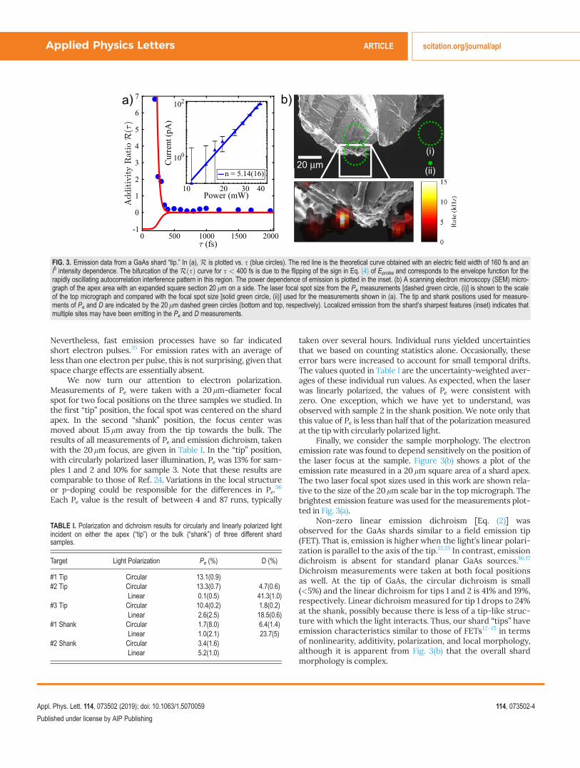
We first consider the electron pulse emission process.Electron emission from nanotips, if measured to be both nonlin-ear and additive for s > slaser, has been shown to be fast.12–14 Ourelectron emission current shows non-linearity as a function ofintensity. It fits with a power law of n¼ 5.14(16) [Fig. 3(a) inset;blue line]. The Keldysh parameter for a solid, c, characterizes theemission. For c� 1, field emission is dominated by multiphotonprocesses.34,35 Given our focal spot sizes of 20lm and 3.6lmand an average power that never exceeded 150 mW, our Keldyshparameter readily satisfied this condition in all our experimentsand supports our simple multi-photon model. The fifth ordernon-linearity indicates a five-photon process. [This result is inexcess of the three-photon process illustrated in Fig. 1(b)].Generally speaking, the order of the multiphoton process in agiven sample can vary with the details of the emitting surface,its local surface electric field, and the nature of surface statesnear the emission point.36
Pump-probe measurements as described above were usedto determine if the emission was additive.12,32 The additivity ratiois defined as
RðsÞ �RbothðsÞ � RpumpðsÞ þ RprobeðsÞ
� �RpumpðsÞ þ RprobeðsÞ
; (3)
where Rpump(s) and Rprobe(s) are the emission rates from thepump and probe beams at each delay respectively, and the rateRboth(s) wasmodeled as
RbothðsÞ ¼ð1�1
EpumpðtÞ6Eprobeðtþ sÞ� �2n dt: (4)
The individual pump and probe field amplitudes were modeledas Gaussians with EðtÞ ¼ E0 exp ½�ðt=spulseÞ2�. The best fit to thedata [red line in Fig. 3(a)] is obtained for spulse¼ 160 fs (n¼ 5). Theelectron emission process is additive [RðsÞ ¼ 0 for s > 400 fs]and is thus shown to be faster than this value. Note that this isnot a direct measurement of the electron pulse duration.
FIG. 2. The experimental setup for polarimetry and dichroism measurements. Thepulsed laser beam (1) enters the chamber and hits the off-axis parabolic mirror (2)which focuses the laser onto the sample (3). Note that the beam is propagating outof the plane at (2), indicated by the red circle. The sample is mounted on an XYZtranslator (4) that allows the sample tip to be positioned in the laser focus. A CEM(5) can be used to monitor electron emission. Transport optics (6) guide emittedelectrons (7) toward the Mott polarimeter (8) in the adjoining chamber with top (T)and bottom (B) CEM detectors. A 260 l/s turbomolecular pump (9) evacuates thechamber.
Nevertheless, fast emission processes have so far indicatedshort electron pulses.35 For emission rates with an average ofless than one electron per pulse, this is not surprising, given thatspace charge effects are essentially absent.
We now turn our attention to electron polarization.Measurements of Pe were taken with a 20lm-diameter focalspot for two focal positions on the three samples we studied. Inthe first “tip” position, the focal spot was centered on the shardapex. In the second “shank” position, the focus center wasmoved about 15lm away from the tip towards the bulk. Theresults of all measurements of Pe and emission dichroism, takenwith the 20lm focus, are given in Table I. In the “tip” position,with circularly polarized laser illumination, Pe was 13% for sam-ples 1 and 2 and 10% for sample 3. Note that these results arecomparable to those of Ref. 24. Variations in the local structureor p-doping could be responsible for the differences in Pe.36
Each Pe value is the result of between 4 and 87 runs, typically
taken over several hours. Individual runs yielded uncertaintiesthat we based on counting statistics alone. Occasionally, theseerror bars were increased to account for small temporal drifts.The values quoted in Table I are the uncertainty-weighted aver-ages of these individual run values. As expected, when the laserwas linearly polarized, the values of Pe were consistent withzero. One exception, which we have yet to understand, wasobserved with sample 2 in the shank position.We note only thatthis value of Pe is less than half that of the polarization measuredat the tip with circularly polarized light.
Finally, we consider the sample morphology. The electronemission rate was found to depend sensitively on the position ofthe laser focus at the sample. Figure 3(b) shows a plot of theemission rate measured in a 20lm square area of a shard apex.The two laser focal spot sizes used in this work are shown rela-tive to the size of the 20lm scale bar in the top micrograph. Thebrightest emission feature was used for the measurements plot-ted in Fig. 3(a).
Non-zero linear emission dichroism [Eq. (2)] wasobserved for the GaAs shards similar to a field emission tip(FET). That is, emission is higher when the light’s linear polari-zation is parallel to the axis of the tip.12,13 In contrast, emissiondichroism is absent for standard planar GaAs sources.16,17
Dichroism measurements were taken at both focal positionsas well. At the tip of GaAs, the circular dichroism is small(<5%) and the linear dichroism for tips 1 and 2 is 41% and 19%,respectively. Linear dichroism measured for tip 1 drops to 24%at the shank, possibly because there is less of a tip-like struc-ture with which the light interacts. Thus, our shard “tips” haveemission characteristics similar to those of FETs12–15 in termsof nonlinearity, additivity, polarization, and local morphology,although it is apparent from Fig. 3(b) that the overall shardmorphology is complex.
FIG. 3. Emission data from a GaAs shard “tip.” In (a), R is plotted vs. s (blue circles). The red line is the theoretical curve obtained with an electric field width of 160 fs and anI5 intensity dependence. The bifurcation of the RðsÞ curve for s < 400 fs is due to the flipping of the sign in Eq. (4) of Eprobe and corresponds to the envelope function for therapidly oscillating autocorrelation interference pattern in this region. The power dependence of emission is plotted in the inset. (b) A scanning electron microscopy (SEM) micro-graph of the apex area with an expanded square section 20 lm on a side. The laser focal spot size from the Pe measurements [dashed green circle, (i)] is shown to the scaleof the top micrograph and compared with the focal spot size [solid green circle, (ii)] used for the measurements shown in (a). The tip and shank positions used for measure-ments of Pe and D are indicated by the 20lm dashed green circles (bottom and top, respectively). Localized emission from the shard’s sharpest features (inset) indicates thatmultiple sites may have been emitting in the Pe and D measurements.
TABLE I. Polarization and dichroism results for circularly and linearly polarized lightincident on either the apex (“tip”) or the bulk (“shank”) of three different shardsamples.
Target Light Polarization Pe (%) D (%)
#1 Tip Circular 13.1(0.9)#2 Tip Circular 13.3(0.7) 4.7(0.6)
Linear 0.1(0.5) 41.3(1.0)#3 Tip Circular 10.4(0.2) 1.8(0.2)
Linear 2.6(2.5) 18.5(0.6)#1 Shank Circular 1.7(8.0) 6.4(1.4)
In summary, we have demonstrated a source that is able toproduce fast pulses of polarized electrons from a micrometer-size area. This can, in principle, enable the imaging of a smallelectron spot on a target to measure spin-dependent effectswith fs-scale resolution. The reduced vacuum requirements ofthis source when compared with NEA GaAs sources make it eas-ier and less costly to operate. Although the observed electronpolarization is modest, our results demonstrate that this sourcefollows the selection rules illustrated in Fig. 1(c). Polarizationmight be increased by having a sharper, more well-defined GaAstip or varying the laser wavelength. The parameter space is largeand open to future study. Through the use of chemical etchingand ion milling, it is possible to shape the tip. An optical para-metric amplifier can be used to explore the wavelength-dependence of polarization. Investigation of the effects theseparameters have on the total yield and polarization of the emit-ted electrons is needed.
We thank M. Becker for useful conversations and S.Keramati for taking the electron micrographs shown in Fig.3(b). This work was funded by NSF Award Nos. PHY-1206067and 1505794 (T.J.G.), EPS-1430519 (H.B. and T.J.G.), and PHY-1602755 (H.B.).
REFERENCES1V. A. Lobastov, R. Srinivasan, and A. H. Zewail, Proc. Natl. Acad. Sci. U. S. A.102, 7069 (2005).
2P. Lougovski and H. Batelaan, Phys. Rev. A 84, 023417 (2011).3E. Jones, M. Becker, J. Luiten, and H. Batelaan, Laser Photonic Rev. 10, 214(2016).
4C. Ropers and M. Kasevich, personal communications (November 30, 2018).5H. Kiesel, A. Renz, and F. Hasselbach, Nature 418, 392 (2002).6T. Kodama, N. Osakabe, and A. Tonomura, Phys. Rev. A 83, 063616(2011).
7G. Baym and K. Shen, “Hanbury Brown-Twiss interferometry with elec-trons: Coulomb vs. quantum statistics,” in In Memory of Akira Tonomura(World Scientific, 2014), pp. 201–210.
8A. H. Zewail, Science 328, 187 (2010).9R. Bormann, S. Strauch, S. Sch€afer, and C. Ropers, J. Appl. Phys. 118, 173105(2015).
10M. T. Hassan, J. S. Baskin, B. Liao, and A. H. Zewail, Nat. Photonics 11, 425(2017).
11W.Wan, L. Yu, L. Zhu, X. Yang, Z. Wei, J. Z. Liu, J. Feng, K. Kunze, O. Schaff,R. Tromp, and W.-X. Tang, Ultramicroscopy 174, 89 (2017).
12B. Barwick, C. Corder, J. Strohaber, N. Chandler-Smith, C. Uiterwaal, andH. Batelaan, New J. Phys. 9, 142 (2007).
13P. Hommelhoff, Y. Sortais, A. Aghajani-Talesh, and M. A. Kasevich, Phys.Rev. Lett. 96, 077401 (2006).
14P. Hommelhoff, C. Kealhofer, and M. A. Kasevich, Phys. Rev. Lett. 97,247402 (2006).
15C. Ropers, D. R. Solli, C. P. Schulz, C. Lienau, and T. Elsaesser, Phys. Rev.Lett. 98, 043907 (2007).
16D. T. Pierce and F. Meier, Phys. Rev. B 13, 5484 (1976).17T. J. Gay, Adv. At. Mol. Phys. 57, 157 (2009).18D. Androic, D. S. Armstrong, A. Asaturyan, T. Averett, J. Balewski, J.Beaufait, R. S. Beminiwattha, J. Benesch, F. Benmokhtar, J. Birchall et al.,Phys. Rev. Lett. 111, 141803 (2013).
19F. Giebels, H. Gollisch, and R. Feder, Phys. Rev. B 87, 035124 (2013).20K. Aulenbacher, J. Schuler, D. v Harrach, E. Reichert, J. R€othgen, A.Subashev, V. Tioukine, and Y. Yashin, J. Appl. Phys. 92, 7536 (2002).
21M. Kuwahara, S. Kusunoki, X. G. Jin, T. Nakanishi, Y. Takeda, K. Saitoh, T.Ujihara, H. Asano, and N. Tanaka, Appl. Phys. Lett. 101, 033102 (2012).
22M. Kuwahara, S. Kusunoki, Y. Nambo, K. Saitoh, X. Jin, T. Ujihara, H. Asano,Y. Takeda, and N. Tanaka, Appl. Phys. Lett. 105, 193101 (2014).
23M. Kuwahara, Y. Nambo, K. Aoki, K. Sameshima, X. Jin, T. Ujihara, H. Asano,K. Saitoh, Y. Takeda, and N. Tanaka, Appl. Phys. Lett. 109, 013108 (2016).
24P. Klaer, F. Schertz, M. Lehr, G. Sch€onhense, and H. J. Elmers, Phys. Rev. B88, 214425 (2013).
25T. Irisawa, T. K. Yamada, and T. Mizoguchi, New J. Phys. 11, 113031 (2009).26Y. Niu and M. Altman, Surf. Sci. 604, 1055 (2010).27M. Kuwahara, T. Nakanishi, S. Okumi, M. Yamamoto, M. Miyamoto, N.Yamamoto, K. Yasui, T. Morino, R. Sakai, K. Tamagaki, and K. Yamaguchi,Jpn. J. Appl. Phys., Part 1 45, 6245 (2006).
28J. K. Bae, L. Cultrera, P. DiGiacomo, and I. Bazarov, Appl. Phys. Lett. 112,154101 (2018).
29M. Pirbhai, J. Knepper, E. T. Litaker, D. Tupa, and T. J. Gay, Phys. Rev. A 88,060701 (2013).
30N. B. Clayburn, E. Brunkow, S. J. Burtwistle, G. H. Rutherford, and T. J. Gay,Rev. Sci. Instrum. 87, 053302 (2016).
31M.W. J. Prins, R. Jansen, and H. van Kempen, Phys. Rev. B 53, 8105 (1996).32E. R. Jones, W. C. Huang, G. Basnet, B. N. Flanders, and H. Batelaan, Appl.Phys. Lett. 112, 263104 (2018).
33C. Kealhofer, S. M. Foreman, S. Gerlich, and M. A. Kasevich, Phys. Rev. B86, 035405 (2012).
34F. V. Bunkin and M. V. Federov, Sov. Phys. JETP 5, 896 (1965).35M. Kr€uger, M. Schenk, M. F€orster, and P. Hommelhoff, J. Phys. B 45,074006 (2012).
36O. Schmidt, M. Bauer, C. Wiemann, R. Porath, M. Scharte, O. Andreyev, G.Sch€onhense, and M. Aeschlimann, Appl. Phys. B 74, 223 (2002).