80
Departme nt of Applied Physics Fe rromagnet ic- Fe rroelect ric Domain Co upl ing in Mult ife rro ic Hete ro st ruct ure s T uomas Lahti ne n DOCTORAL DISSERTATIONS
9HSTFMG*afcdae+
ISBN 978-952-60-5230-4 ISBN 978-952-60-5231-1 (pdf) ISSN-L 1799-4934 ISSN 1799-4934 ISSN 1799-4942 (pdf) Aalto University School of Science Department of Applied Physics www.aalto.fi
BUSINESS + ECONOMY ART + DESIGN + ARCHITECTURE SCIENCE + TECHNOLOGY CROSSOVER DOCTORAL DISSERTATIONS
Aalto-D
D 10
6/2
013
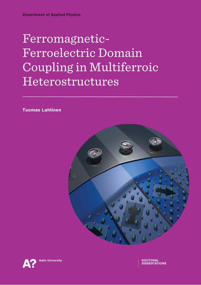
Historically used for navigation; currently utilized in data storage, actuators and sensors—magnetic devices are an indispensible part of our daily lives. However, current magnetic technologies are too complex to incorporate into electronics as components continue to miniaturize. Using an electric field to control magnetism could lead to a new generation of simple, low power magnetic devices. This thesis focuses on domain coupling in multiferroic heterostructures, a group of hybrid materials that couple electric-field-sensitive ferroelectric materials and magnetic-field-sensitive ferromagnetic materials. As a key result, electric field controlled local magnetization rotation and magnetic domain wall motion are demonstrated.
Tuom
as Lahtinen
Ferrom
agnetic-Ferroelectric D
omain C
oupling in Multiferroic H
eterostructures A
alto U
nive
rsity
Department of Applied Physics
Ferromagnetic-Ferroelectric Domain Coupling in Multiferroic Heterostructures
Tuomas Lahtinen
DOCTORAL DISSERTATIONS
Aalto University publication series DOCTORAL DISSERTATIONS 106/2013
Ferromagnetic-Ferroelectric Domain Coupling in Multiferroic Heterostructures
Tuomas Lahtinen
A doctoral dissertation completed for the degree of Doctor of Science (Technology) to be defended, with the permission of the Aalto University School of Science, at a public examination held at the lecture hall E of the Main Building on 27 June 2013 at 12.
Aalto University School of Science Department of Applied Physics Nanomagnetism and Spintronics
Supervising professor Prof. Sebastiaan van Dijken Thesis advisor Prof. Sebastiaan van Dijken Preliminary examiners Dos. Marina Tyunina, University of Oulu, Finland Prof. Petriina Paturi, University of Turku, Finland Opponent Dr. Neil Mathur, University of Cambridge, United Kingdom
Aalto University publication series DOCTORAL DISSERTATIONS 106/2013 © Tuomas Lahtinen ISBN 978-952-60-5230-4 (printed) ISBN 978-952-60-5231-1 (pdf) ISSN-L 1799-4934 ISSN 1799-4934 (printed) ISSN 1799-4942 (pdf) http://urn.fi/URN:ISBN:978-952-60-5231-1 Unigrafia Oy Helsinki 2013 Finland
Abstract Aalto University, P.O. Box 11000, FI-00076 Aalto www.aalto.fi
Author Tuomas Lahtinen Name of the doctoral dissertation Ferromagnetic-Ferroelectric Domain Coupling in Multiferroic Heterostructures Publisher School of Science Unit Department of Applied Physics
Series Aalto University publication series DOCTORAL DISSERTATIONS 106/2013
Field of research Multiferroic heterostructures
Manuscript submitted 16 April 2013 Date of the defence 27 June 2013
Permission to publish granted (date) 17 May 2013 Language English
Monograph Article dissertation (summary + original articles)
Abstract In this thesis, strain-mediated coupling between magnetic films and ferroelectric BaTiO3
substrates with regular ferroelastic domain structures is studied. Using optical polarization microscopy, it is shown that imprinting of ferroelectric domains into magnetic polycrystalline CoFe, amorphous CoFeB and crystalline Fe films can be achieved. The ferroelectric polarization and elongated c-axis of the BaTiO3 substrates rotate by 90o at ferroelectric domain boundaries. Transfer of this strain to the adjacent magnetic film induces local magnetoelastic anisotropy whose orientation and symmetry depends on the underlying ferroelectric domain. Furthermore, abrupt changes in the magnetoelastic anisotropy pin the magnetic domain walls onto the ferroelectric domain boundaries. As a result, the magnetic domain walls do not move in an applied magnetic field resulting in the formation of magnetically charged and uncharged domain walls at different field directions.
The strong coupling between magnetic and ferroelectric domains is used to demonstrate local magnetic switching and magnetic domain wall motion by purely electrical means. It is shown that a regular magnetic stripe pattern can be reversibly written and erased by the application of an electric field across the BaTiO3 substrate. Moreover, the magnetic domain walls are dragged along by their ferroelectric counterpart in an external electric field. Both effects are explained by 90o rotations of the ferroelectric polarization and the resulting strain-induced modification of the local magnetoelastic anisotropy. Similar strain-mediated effects, including local in-plane magnetization rotation by 90o, are obtained when the multiferroic heterostructures are cooled or heated through the structural phase transitions of BaTiO3.
Keywords ferromagnetic, ferroelectric, multiferroic, magnetism, magnetic domain, electric field control of magnetism, Barium Titanate
ISBN (printed) 978-952-60-5230-4 ISBN (pdf) 978-952-60-5231-1
ISSN-L 1799-4934 ISSN (printed) 1799-4934 ISSN (pdf) 1799-4942
Location of publisher Espoo Location of printing Espoo Year 2013
Pages 119 urn http://urn.fi/URN:ISBN:978-952-60-5231-1

Preface
Five years ago I started my Ph.D. studies in the new Nanomagnetism and Spin-
tronics group (NanoSpin) at Aalto University as the first full-time group mem-
ber. The topic of my research was electric field controlled magnetism, a rela-
tively new and ambitious research field. During my time at NanoSpin, the lab-
oratories have filled with new equipment, new members have joined the group
and the group has established itself within the magnetic research community.
The experiences I have gained during these years have been of utmost value.
I am forever grateful to those, who have assisted and supported me during my
academic career.
First and foremost, I would like to thank my supervisor, Prof. Sebastiaan van
Dijken, for the countless hours he has invested in me. Without his guidance,
knowledge, experience and intuition none of the work presented in this thesis
would have been possible. It has been a pleasure working with Sebastiaan
through these years.
I would also like to thank the successful collaborations that have been the
backbone of this work. The magnetic modeling performed by Mr. Jussi Tuomi
and Mr. Kévin Franke have played an integral role in the publications and I
am grateful for their contributions. I would like to thank Dr. Qi Hang Qin and
Mr. Witold Skowronski for helping me with cleanroom techniques and trans-
port measurements. I would also like to thank Dr. Lide Yao, Dr. Yang-Jong
Kim, Dr. Arianna Casiraghi, Dr. Sayani Majumdar, Mr. Mikko Kataja, Mr.
Sampo Hämäläinen, Mr. Jukka Kärkimaa and especially Mrs. Laura Äkäs-
lompo. I have been fortunate enough to work with these talented individuals
of the NanoSpin group and I thank them for their support, assistance and in-
sightful discussions.
Our group has enjoyed a close relationship with the Quantum Dynamics
group. I would like to thank Dr. Francesco Massel, Dr. Jussi Kajala, Dr. Jami
Kinnunen, Dr. Jani Martikainen, Dr. Dong-Hee Kim, Mr. Miikka Heikkinen
i
Preface
and Mr. Antti-Pekka Eskelinen for providing a social and enjoyable working
environment.
I would also like to acknowledge the National Doctoral Programme in Mate-
rials Physics and Eemil Aaltosen säätiö for funding.
Finally, I dedicate this thesis to those closest to me, my family. I cannot
express enough gratitude towards my parents, who have always supported me
and my choices in life. Their contribution is immeasurable. I am most grateful
to my girlfriend, Miss Marianne Jokinen, who has supported me throughout my
Ph.D. studies and for her unconditional love and support. I am, truly, privileged
to have her by my side.
Espoo, May 28, 2013,
Tuomas H. E. Lahtinen
ii
Contents
Preface i
Contents iii
List of Publications v
Author’s Contribution vii
1. Introduction 1
2. Ferromagnetism 3
2.1 Exchange energy . . . . . . . . . . . . . . . . . . . . . . . . . . . . . . 4
2.2 Magnetostatic energy . . . . . . . . . . . . . . . . . . . . . . . . . . . 4
2.3 Magnetic anisotropy . . . . . . . . . . . . . . . . . . . . . . . . . . . . 5
2.3.1 Magnetocrystalline anisotropy . . . . . . . . . . . . . . . . . 5
2.3.2 Magnetoelastic anisotropy . . . . . . . . . . . . . . . . . . . . 6
2.4 Zeeman energy . . . . . . . . . . . . . . . . . . . . . . . . . . . . . . . 7
2.5 Magnetic domains and domain walls . . . . . . . . . . . . . . . . . . 7
2.5.1 Magnetization reversal . . . . . . . . . . . . . . . . . . . . . . 10
3. Ferroelectricity 15
3.1 Barium Titanate . . . . . . . . . . . . . . . . . . . . . . . . . . . . . . 16
3.1.1 Structure . . . . . . . . . . . . . . . . . . . . . . . . . . . . . . 16
3.1.2 Domains . . . . . . . . . . . . . . . . . . . . . . . . . . . . . . . 17
4. Multiferroics 21
4.1 Single-phase multiferroics . . . . . . . . . . . . . . . . . . . . . . . . 21
4.2 Multiferroic heterostructures . . . . . . . . . . . . . . . . . . . . . . 22
4.2.1 Charge modulation . . . . . . . . . . . . . . . . . . . . . . . . 23
4.2.2 Exchange interaction . . . . . . . . . . . . . . . . . . . . . . . 23
4.2.3 Strain transfer . . . . . . . . . . . . . . . . . . . . . . . . . . . 24
iii

Contents
5. Experimental Methods and Modeling 27
5.1 Thin film growth . . . . . . . . . . . . . . . . . . . . . . . . . . . . . . 27
5.1.1 Electron beam evaporation . . . . . . . . . . . . . . . . . . . . 28
5.1.2 Molecular beam epitaxy . . . . . . . . . . . . . . . . . . . . . 30
5.1.3 Magnetron sputtering . . . . . . . . . . . . . . . . . . . . . . . 30
5.2 Magneto-optics . . . . . . . . . . . . . . . . . . . . . . . . . . . . . . . 32
5.2.1 Magneto-optical Kerr effect . . . . . . . . . . . . . . . . . . . 33
5.2.2 Magneto-optical Kerr microscopy . . . . . . . . . . . . . . . . 33
5.2.3 Electric field and temperature measurements . . . . . . . . 35
5.3 Magnetic modeling . . . . . . . . . . . . . . . . . . . . . . . . . . . . . 35
5.3.1 Macrospin model . . . . . . . . . . . . . . . . . . . . . . . . . . 36
5.3.2 Micromagnetic simulations . . . . . . . . . . . . . . . . . . . 37
6. Results and Discussion 39
6.1 Pattern transfer . . . . . . . . . . . . . . . . . . . . . . . . . . . . . . 39
6.1.1 CoFe/BaTiO3 . . . . . . . . . . . . . . . . . . . . . . . . . . . . 39
6.1.2 Fe/BaTiO3 . . . . . . . . . . . . . . . . . . . . . . . . . . . . . . 43
6.1.3 CoFeB/BaTiO3 . . . . . . . . . . . . . . . . . . . . . . . . . . . 45
6.2 Electric field control of magnetization and magnetic domain wall
motion . . . . . . . . . . . . . . . . . . . . . . . . . . . . . . . . . . . . 49
6.3 Temperature control of magnetic anisotropy . . . . . . . . . . . . . 52
7. Conclusions 57
Bibliography 59
Publications 67
iv

List of Publications
This thesis consists of an overview and of the following publications which are
referred to in the text by their Roman numerals.
I Tuomas H. E. Lahtinen, Jussi O. Tuomi, Sebastiaan van Dijken. Pattern
Transfer and Electric-Field Induced Magnetic Domain Formation in Multi-
ferroic Heterostructures. Advanced Materials, 23, 3187-3191, September 2011.
II Tuomas H. E. Lahtinen, Jussi O. Tuomi, Sebastiaan van Dijken. Electri-
cal Writing of Magnetic Domain Patterns in Ferromagnetic/Ferroelectric Het-
erostructures. IEEE Transactions on Magnetics, 47, 3768-3771, October 2011.
III Tuomas H. E. Lahtinen, Kévin J. A. Franke, Sebastiaan van Dijken. Electric-
Field Control of Magnetic Domain Wall Motion and Local Magnetization Rev-
ersal. Scientific Reports, 2, 258, February 2012.
IV Kévin J. A. Franke, Tuomas H. E. Lahtinen, Sebastiaan van Dijken. Field
Tuning of Ferromagnetic Domain Walls on Elastically Coupled Ferroelectric
Domain Boundaries. Physical Review B, 85, 094423, March 2012.
V Tuomas H. E. Lahtinen, Yasuhiro Shirahata, Lide Yao, Kévin J. A. Franke,
Gorige Vemkataiah, Tomoyasu Taniyama, Sebastiaan van Dijken. Alternat-
ing Domains with Uniaxial and Biaxial Magnetic Anisotropy in Epitaxial Fe
Films on BaTiO3. Applied Physics Letters, 101, 262405, December 2012.
VI Tuomas H. E. Lahtinen, Sebastiaan van Dijken. Temperature Control of
Local Magnetic Anisotropy in Multiferroic CoFe/BaTiO3. Applied Physics Let-
v
List of Publications
ters, 102, 112406, March 2013.
vi
Author’s Contribution
Publication I: “Pattern Transfer and Electric-Field Induced MagneticDomain Formation in Multiferroic Heterostructures”
The author designed the experiments, grew and characterized the samples
by XRD and optical polarization microscopy, carried out the electric-field ex-
periments, analyzed the data, discussed the results with co-authors and con-
tributed to writing the manuscript.
Publication II: “Electrical Writing of Magnetic Domain Patterns inFerromagnetic/Ferroelectric Heterostructures”
The author designed the experiments, grew and characterized the samples by
XRD and optical polarization microscopy, analyzed the data, discussed the re-
sults with co-authors and contributed to writing the manuscript.
Publication III: “Electric-Field Control of Magnetic Domain WallMotion and Local Magnetization Reversal”
The author designed the experiments, grew and characterized the samples by
XRD and optical polarization microscopy, carried out the electric-field-control
experiments, analyzed the data, discussed the results with co-authors and con-
tributed to writing the manuscript.
vii
Author’s Contribution
Publication IV: “Field Tuning of Ferromagnetic Domain Walls onElastically Coupled Ferroelectric Domain Boundaries”
The author designed the experiments, grew and characterized the samples by
XRD and optical polarization microscopy.
Publication V: “Alternating Domains with Uniaxial and BiaxialMagnetic Anisotropy in Epitaxial Fe Films on BaTiO3”
The author characterized the samples by optical polarization microscopy, ana-
lyzed the data, discussed the results with co-authors and contributed to writing
the manuscript.
Publication VI: “Temperature Control of Local Magnetic Anisotropyin Multiferroic CoFe/BaTiO3”
The author designed the experiments, grew and characterized the samples by
XRD and optical polarization microscopy, carried out the temperature-controlled
experiments, analyzed the data, discussed results with co-authors and wrote
the manuscript with help from co-author.
viii
1. Introduction
Magnetic materials are currently used for a wide range of practical applica-
tions including magnetic memory, and magnetic field sensors and actuators.
The ability to control magnetism with an electric field has drawn wide research
interest due to the potential it holds in lowering the power consumption of mag-
netic devices [1]. However, electric fields do not interact with magnetic mate-
rials. Multiferroic heterostructures are hybrid materials that combine both
magnetic- and electric-field-sensitive ferroelectric materials. It has been shown
that these materials exhibit a magnetic response in an electric field if the mag-
netic and ferroelectric materials couple.
One popular approach is to elastically couple magnetic thin films to ferroele-
ctric substrates. Strain transfer from the ferroelectric substrate influences the
properties of the magnetic film through inverse magnetostriction. In this work,
microscopic aspects of this coupling mechanism are investigated in detail. In
particular, correlations between the domain patterns of the ferroelectric sub-
strates and magnetic films are imaged as a function of magnetic field, electric
field and temperature.
This thesis starts with an introduction to ferromagnetism and magnetic ma-
terials with a focus on the energies that govern magnetic domain formation
and the structure of magnetic domain walls (Chapter 2). A summary of ferro-
electric BaTiO3 including the ferroelectric domain structures and temperature
related structural phase transitions follows (Chapter 3). Finally, Chapter 4
gives an overview of multiferroic materials and recent advances in electric field
controlled magnetism in multiferroic systems.
The introductory Chapters are followed by an outline of the experimental
methods, including thin film preparation methods and optical microscopy tech-
niques (Chapter 5). The multiferroic heterostructures under study consist of
ferroelectric BaTiO3 substrates with magnetic CoFe, CoFeB and Fe films grown
on top. Optical polarization microscopy measurements in conjunction with
1
Introduction
a macrospin model and micromagnetic simulations are used to analyze the
physics of these samples. An optical polarization microscopy technique is used
for the first time to image ferroelectric and ferromagnetic domains simultane-
ously. This provides a platform to image domain evolution during magnetic and
electric field controlled experiments.
Finally, Chapter 6 summarizes the main results of this thesis. Imprinting
of ferroelectric domain patterns into magnetic films through interfacial strain
transfer is demonstrated by imaging ferroelectric and magnetic domains and
measuring local magnetic hysteresis curves. Subsequently, electric field and
temperature controlled experiments indicate robust coupling of magnetic do-
mains to their ferroelectric counterparts. As a key result, electric-field-induced
magnetic domain control and magnetic domain wall motion in zero applied
magnetic field are demonstrated.
2

2. Ferromagnetism
The characteristic feature of a ferromagnetic material is it’s spontaneous mag-
netization, which is caused by alignment of atomic magnetic moments within
the material. In ferromagnetic materials, the magnetic moment of the atoms
originates in the electrons’ spin, and their orbital motion around the nucleus.
The spin-orbit interaction describes the coupling of the magnetic moments pro-
duced by the electron’s spin with it’s orbital motion around the nucleus.
A spin imbalance occurs in electron shells that are not full. The Pauli Ex-
clusion Principle prevents electrons in the same quantum state from aligning
their spins parallel. In many-electron electron shells the Coulomb force repels
electrons that are in close proximity. To minimize the Coulomb energy, elec-
trons align their spins parallel and fill the different quantum states first. This
results in an unequal number of the two spin states giving the atom a net elec-
tron spin. Atoms with completely filled electron shells cannot be magnetic. In
ferromagnetic 3-d transition metals such as Ni, Co and Fe the atomic magnetic
moments primarily originate from the imbalance between the two spin states
and the contribution of the orbital motion is relatively small [2].
The spontaneous magnetization of ferromagnetic materials originates from
long-range ordering of atomic moments. Assuming localized electrons, the align-
ment of atomic moments can be described by the Heisenberg Hamiltonian
H =−∑Ji jSi ·Sj, (2.1)
where Ji j is the exchange integral and Si, Sj are localized atomic spins. In fer-
romagnetic materials Ji j > 0 causing neighboring spins to align parallel. Due
to the exchange interaction, atomic moments align below an ordering tempera-
ture Tc known as the Curie temperature. Above Tc, ferromagnetic ordering is
overcome by thermal fluctuations [3].
The overall behavior of the magnetization in ferromagnetic materials is a
competition between exchange, magnetostatic and anisotropy energies. Al-
3

Ferromagnetism
though the exchange energy dominates at small length scales, magnetostatic
and anisotropy energies influence long-range magnetic ordering [4]. This Chap-
ter provides an overview of the different energy contributions in ferromagnetic
systems and their influence on magnetic domain formation and the intrinsic
properties of magnetic domain walls.
2.1 Exchange energy
Exchange energy dominates the alignment of atomic moments at small length
scales, aligning atomic moments parallel in ferromagnetic systems. The di-
rect exchange interaction that is present between atomic spins is described by
Equation 2.1. The exchange interaction results in an exchange energy density
(∼ 0.1eV/atom [5]), which can be expressed as [6]
Eex = A(∇m)2 (2.2)
where m = M/MS is the magnetization unit vector and A is the exchange
stiffness constant.
2.2 Magnetostatic energy
Magnetostatic energy originates from free surface magnetic poles at an inter-
face. In a uniformly magnetized sample stray fields are created outside the
magnetic material and a demagnetizing field within the magnetic element. Al-
though the magnetostatic energy is significantly smaller (∼ 0.1meV/atom [5])
than the exchange energy it operates over longer length scales. The magnetic
pole strength per unit surface area σ can be written as the component of mag-
netization perpendicular to an interface [7]
σ=M ·n, (2.3)
where n is the unit vector normal to the interface. The magnetostatic energy
density due to magnetic stray fields at the interface can be expressed as [8,9]
Ems =−(μ0
2
)Hd ·M, (2.4)
where Hd is the magnetic dipolar field created by the magnetization. This re-
sults in a demagnetizing field, which anti-aligns with the magnetization inside
the magnetic sample. For an arbitrary shape the demagnetizing field is given
4
Ferromagnetism
by
Hd =−NM, (2.5)
where the demagnetizing tensor N is equal to unity for thin films with per-
pendicular magnetization.
2.3 Magnetic anisotropy
Magnetic anisotropy describes the angular dependence of magnetic energy. In
a magnetic system containing anisotropy, the easy axes are defined as the mag-
netization orientation with minimum magnetic anisotropy energy and the hard
axes are aligned along directions with maximum energy. A measure of the
anisotropy strength is the anisotropy constant Ki, which is an energy density
associated with an anisotropy contribution, i.
Magnetocrystalline and magnetoelastic contributions dominate the magnetic
anisotropy landscape in the multiferroic systems studied in this thesis. The
origins of these anisotropies are discussed in more detail below.
2.3.1 Magnetocrystalline anisotropy
Magnetocrystalline anisotropy arises from the symmetry of crystalline lattices
and the elongated charge distribution around atoms due to the spin-orbit cou-
pling. If we expand the free energy of a cubic magnetocrystalline system, Ec in
terms of the directional cosines, m1, m2 and m3, where mi = Mi/MS, we get [6]
Ec = K1(m21m2
2 +m21m2
3 +m22m2
3)+K2(m21m2
2m23) . . . , (2.6)
where K1 and K2 are first and second order anisotropy constants. In crude
terms, the sign of K1 determines whether ⟨001⟩ or ⟨111⟩ are the magnetocrys-
talline easy axes. As an example, Fe has magnetocrystalline easy axes along
⟨001⟩ (K1 > 0), while in Ni the magnetocrystalline easy axes are along ⟨111⟩(K1 < 0) [10–13].
Amorphous ferromagnetic materials exhibit no magnetocrystalline anisot-
ropy as no crystal symmetry is present. Similarly, completely randomly ori-
ented polycrystalline materials will exhibit small magnetocrystalline anisot-
ropy as the magnetocrystalline anisotropies of the individual grains cancel over
macroscopic length scales.
5

Ferromagnetism
2.3.2 Magnetoelastic anisotropy
Applying a mechanical strain to a ferromagnetic material induces a magne-
toelastic anisotropy, otherwise known as the inverse magnetostriction effect
[14, 15]. The strength of the magnetoelastic anisotropy is proportional to the
stress σ and magnetostriction λs of the material. The magnetoelastic anisot-
ropy constant Kme for isotropic materials can be written as [6]
Kme =−3σλs
2, (2.7)
where σ is proportional to the strain ε via Young’s modulus Y . Isotropic sys-
tems include polycrystalline films with random texture and amorphous films
[16]. Magnetoelastic anisotropy in amorphous systems originates from so-called
bond-orientation anisotropy, where the anisotropy depends on average bond
lengths [15,17–21]. Applying a tensile strain to an amorphous system increases
the average bond length along the direction of strain leading to magnetoelastic
anisotropy. The anisotropy energy of an isotropic system experiencing uniaxial
strain can be written as
Eme =−Kme sin2φ, (2.8)
where φ is the angle between the magnetization and the strain axes. The
magnetoelastic easy axis can either lie parallel or perpendicular to the direction
of uniaxial strain. The sign of the magnetostriction λs of the material and the
sign of the strain ε dictate the sign of Kme. As an example, if a film experiences
uniaxial tensile strain (ε> 0) and has a positive magnetostriction then Kme < 0
leading to minima of Eme lying parallel to the direction of the tensile strain
axis. If the same material were to experience a compressive strain (ε < 0) the
magnetoelastic easy axis would lie perpendicular to the strain axis.
For crystalline systems the magnetoelastic anisotropy contribution depends
on the direction of strain with respect to the crystalline axes. The general form
of magnetoelastic energy in a crystalline system can be written as [22]
Eme = B1(α2
1εx +α22εy +α2
3εz)
+B2(α1α2εxy +α2α3εyz +α3α1εzx
), (2.9)
where Bi are the magnetoelastic anisotropy constants, αi are the directional
cosines of the magnetization with respect to the crystalline axes, εi are normal
strains along the crystalline axes and εi j are shear strains.
6
Ferromagnetism
In epitaxial systems the magnetocrystalline anisotropy (Equation 2.6) and
the magnetoelastic anisotropy (Equation 2.9) both contribute to the total ani-
sotropy energy. For a crystalline material experiencing normal strain the mag-
netoelastic anisotropy dominates the magnetocrystalline anisotorpy above a
critical strain value εc, which can be written as
εc = |K1||B1|
. (2.10)
For example, using bulk values for Fe (K1 = 4.8×10⁴J/m3, B1 =−2.9×10⁶J/m3
[6]) this gives εc = 1.7%, i.e. above 1.7% lattice strain the magnetoelastic ani-
sotropy becomes the dominant anisotropy contribution.
2.4 Zeeman energy
The Zeeman energy describes how the magnetization of a sample interacts with
an external magnetic field. The Zeeman energy can be written as
Ez =−μ0
∫M ·HdV , (2.11)
where H is the external magentic field and M is the sample magnetization.
For uniform magnetization and uniform external magnetic field this can be
written as an energy density,
Ez =−μ0MsH cos(φ−θ
), (2.12)
where(φ−θ
)is the angle between M and H and Ms is the saturation magne-
tization.
2.5 Magnetic domains and domain walls
The competition between the short-range exchange energy and long-range mag-
netostatic energy leads to magnetic domain formation [23]. Magnetic domains
are areas of uniform magnetization separated by magnetic domain walls.
The exchange length indicates the length below which inter-atomic exchange
interactions dominate and can be written as [24]
lex =(A/μ0M2
S)1/2
, (2.13)
where A is the exchange stiffness and Ms is saturation magnetization. Mag-
netic domain formation is favorable when the size of a magnetic structure be-
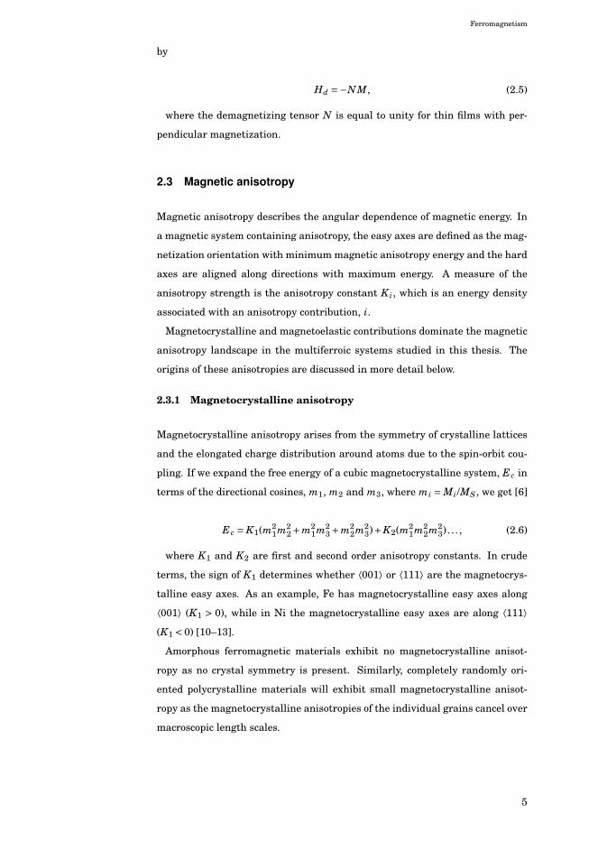
comes larger than lex. Figure 2.1 (a) illustrates magnetic domain formation in
7
Ferromagnetism
(c)
M
H = 0
(a)
M
e.a.
H = 0
(b)
M
Figure 2.1. Schematic illustrations of different magnetization states, black arrows indicate di-rection of M. Magnetostatic stray fields are contained to within the sample in anisotropic system by the formation of domains, shown in (a). Domain formation in auniaxial anisotropy system is shown in (b), where the easy axis is denoted by e.a.A mono-domain consisting of uniform magnetization along an external magneticfield H is shown in (c). Field lines indicate magnetostatic stray fields created at thesurface. Adapted from [26].
an isotropic magnetic system with no applied external magnetic field. To mini-
mize the magnetostatic, energy the magnetization aligns parallel to the sample
edges. If a uniaxial anisotropy is present (i.e. magnetocrystalline or magnetoe-
lastic), the majority of the magnetization will align along the uniaxial easy axis.
To reduce the magnetostatic energy small ‘closure’ domains form with magne-
tization perpendicular to the magnetic easy axis near the bottom and top edges
of the magnetic structure, as shown in Figure 2.1 (b). The energy penalty for
having magnetization along the hard axis is compensated by a minimization of
the magnetostatic energy.
If a magnetic sample is placed in an external magnetic field (H), the Zeeman
energy Ez will force the magnetization to align with H above the saturation
field. This creates a mono-domain state where the magnetization over the en-
tire sample is uniform, as shown in Figure 2.1 (c). The total energy of magnetic
domains can be written as the sum of the different energy contributions [25]:
Edomain = Eex +Ems +Ec +Eme +Ez. (2.14)
The width of domain walls (δw) that separates magnetic domains is deter-
mined by a competition between the exchange energy and the magnetic ani-
sotropy. Large exchange stiffness widens the domain walls as it minimizes the
magnetization rotation between neighboring atomic spins. On the other hand,
a large magnetic anisotropy decreases the domain wall width to minimize the
energy penalty for having the magnetization pointing away from the magnetic
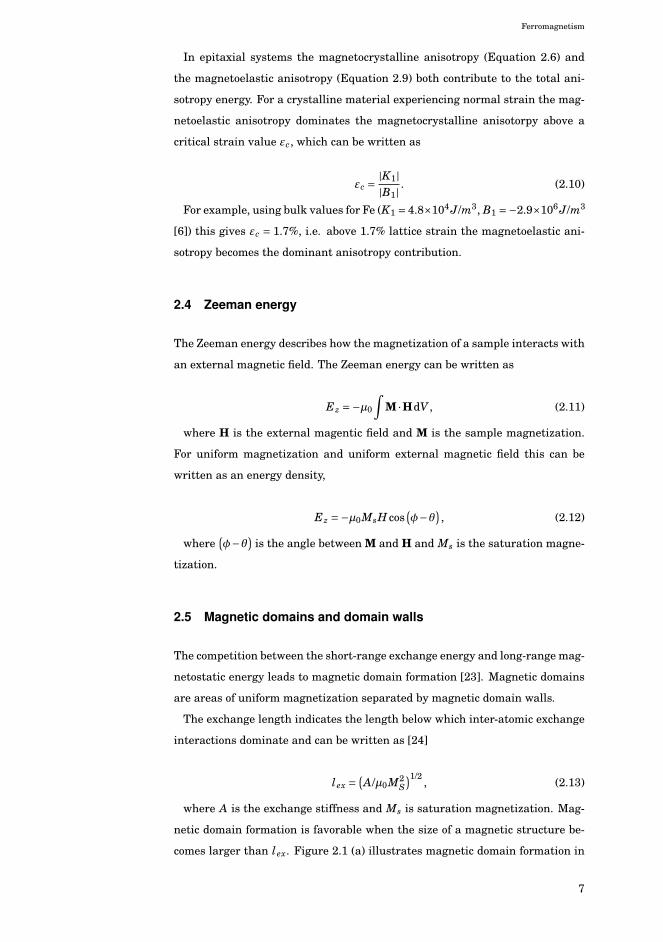
easy axis inside the domain wall. In magnetic films, two types of domain walls
can exist; the Bloch and Néel wall, shown schematically in Figure 2.2.
In a 180◦ Bloch wall the magnetization rotates out-of-plane in the wall. For
8
Ferromagnetism
(a)
(b)
Figure 2.2. Illustration of (a) a Néel domain wall and (b) a Bloch domain wall in magnetic films.
180◦ Bloch walls the domain wall width can be written as [6]
δ∥B =π
(A
Ku
)1/2, (2.15)
where A is the exchange stiffness and Ku is the uniaxial anisotropy constant.
Bloch walls are energetically favorable for thick magnetic films.
In thin magnetic films with uniaxial anisotropy the magnetization rotates in
the plane of the film. This results in 180◦–Néel type domain walls, illustrated in
Figure 2.2. Here, the magnetization points perpendicular to the domain wall in
the center of the wall creating magnetostatic stray fields between the domains.
The resulting magnetostatic energy increases linearly with film thickness in a
Néel wall, therefore, Néel walls are limited to thin magnetic films. No simple
formula exists for the Néel domain wall width as it depends not only on the
exchange stiffness and magnetic anisotropy of the material but also on mag-
netostatic interactions within the domain wall. The width of a Néel wall can
be determined by micromagnetic simulations. To determine the domain wall
width from micromagnetic simulations the spin rotation across the wall is ex-
tracted. The following definition for domain wall width is used in this work:
δ=∫
cos2φdx, (2.16)
where x lies perpendicular to the domain wall and φ is the spin rotation in
the domain wall.
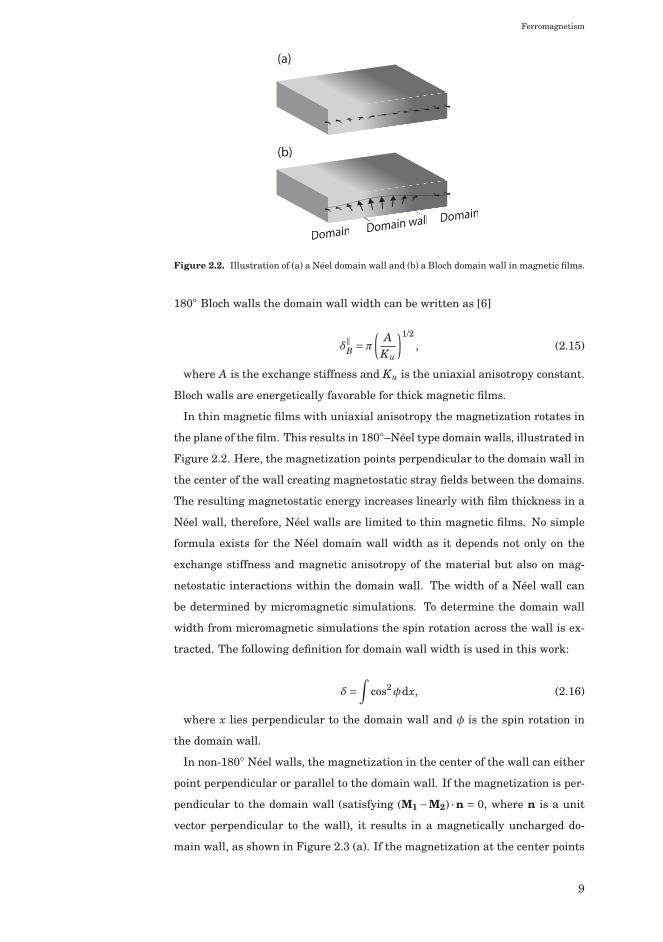
In non-180◦ Néel walls, the magnetization in the center of the wall can either
point perpendicular or parallel to the domain wall. If the magnetization is per-
pendicular to the domain wall (satisfying (M1 −M2) ·n = 0, where n is a unit
vector perpendicular to the wall), it results in a magnetically uncharged do-
main wall, as shown in Figure 2.3 (a). If the magnetization at the center points
9

Ferromagnetism
(a)
(b)
+ +
+ +
+ -+ -
Uncharged
Charged
Figure 2.3. Uncharged Néel type domain wall (a) and charged domain wall (b).
along the domain wall, the magnetization in neighboring domains is aligned in
a head-to-head or tail-to-tail configuration, which results in the accumulation of
magnetic charges (Figure 2.3 (b)). The width of charged domain walls is about
one order of magnitude wider than uncharged domain walls. In bulk magnetic
samples the large magnetostatic energy associated with charged domain walls
makes them unfavorable. However, in thin films their energy reduces with
thickness, which makes their formation more favorable. In the multiferroic
heterostructures under study in this thesis, pinning of magnetic domain walls
on ferroelectric domain boundaries allows for the controlled formation of un-
charged and charged domain walls by an appropriate selection of the magnetic
field direction.
2.5.1 Magnetization reversal
The response of a magnetic film to an external magnetic field is characterized by
a M−H loop, shown in Figure 2.4. The M−H loop indicates the projection of the
magnetization vector onto the axis of the external magnetic field. In a magnetic
system with uniaxial anisotropy the shape of the hysteresis curve depends on
the angle of the magnetic field with respect to the easy anisotropy axis. The
Stoner-Wohlfarth model can be used to describe magnetization behavior in a
magnetic system with uniaxial anisotropy. The model assumes a mono-domain
system with energy density
E =−Ku cos2 (φ
)−μ0HMs cos(φ−θ
), (2.17)
where φ is the angle between the magnetization and the easy anisotropy axis
and θ is the angle between the external magnetic field and the easy anisotropy
axis.
Two instances of the Stoner-Wohlfarth model are considered here; magneti-
10

Ferromagnetism
H
M
Virgin curve
Saturation
Hc
Mr
+Hsat
-Hsat
Figure 2.4. A schematic of a M − H loop for a ferromagnetic material. Mr is the remanentmagnetization and Hc is the coercive field. Magnetic saturation is achieve when|H| > |Hsat|.
zation reversal with the applied magnetic field along the easy anisotropy axis
(θ = 0◦) and along the hard axis (θ = 90◦) of a magnetic material.
Easy axis. As the magnetization lies along the easy axis the anisotropy exerts
no torque on the magnetization. In this case, the magnetization remains
fixed until it rotates abruptly once the external magnetic field is reversed
to a value of Hs = Ku/2μ0Ms. This is schematically shown in Figure 2.5.
Hard axis. When measuring a hysteresis curve along a uniaxial hard axis (θ =90◦) a competition between the anisotropy and Zeeman energy exists. At
zero applied magnetic field the magnetization will align with the easy
axis. Applying a magnetic field perpendicular to the easy axis increases
the Zeeman energy and causes the magnetization to rotate away from
the easy axis. Figure 2.5 shows the linear slope of a hysteresis curve
measured along the hard axis. The magnetization continues to rotate
(known as coherent rotation, illustrated in Figure 2.6) until it saturates
at the saturation field Hsat = Ku/2μ0Ms.
The slope of the hard axis hysteresis curve can be used to determine the
uniaxial anisotropy strength. The energy minima of Equation 2.17 are
first determined by derivation with respect to φ:
dEu
dφ= 2Ku sin(φ)cos(φ)+μ0MsH sin(φ−θ)= 0. (2.18)
As we are dealing with a hard axis measurement we can set θ = 90◦. After
rearranging, this gives
Ku = μ0MsH2sin(φ)
. (2.19)
11

Ferromagnetism
(a) (b)
H/Hs
+1
+1
-1 +1-1
-1
+1
-1
H/Hsat
Figure 2.5. Schematics of hysteresis curves extracted from the Stoner-Wohlfarth model for asystem with uniaxial anisotropy. (a) Shows an easy axis hysteresis curve and (b)and hard axis hysteresis curve.
The slope β around H = 0 of a hard axis hysteresis measurement with a
normalized y-axis can be written β= sin(φ)/μ0H, using units of Tesla for
H. Substituting β gives
Kme = Ms
2β, (2.20)
where Ms is the saturation magnetization of the magnetic film.
In uniform 2-D thin films, magnetization reversal mostly occurs thro-
ugh inverse domain nucleation and subsequent domain wall motion, as
schematically shown in 2.6 (b). If the dimensions of a magnetic film are
sufficiently large (� δdw), small inhomogeneities in the energy landscape
can cause spontaneous domain nucleation during magnetization rever-
sal. The energy required to move a domain wall is often smaller than the
domain nucleation energy and therefore the nucleated domain expands
by lateral domain wall motion. Domain wall motion is hampered by pin-
ning sites include grain boundaries, surface roughness and precipitates
etc. [27–29]. The multiferroic heterostructures in this thesis are charac-
terized by strong magnetic domain wall pinning on ferroelectric domain
boundaries due to abrupt lateral modulations in the magnetic anisot-
ropy. As a result, the magnetization mostly reverses by coherent rota-
tion within the domains, which can be described by the Stoner–Wohlfarth
model.
12
Ferromagnetism
(a) (b)
MM
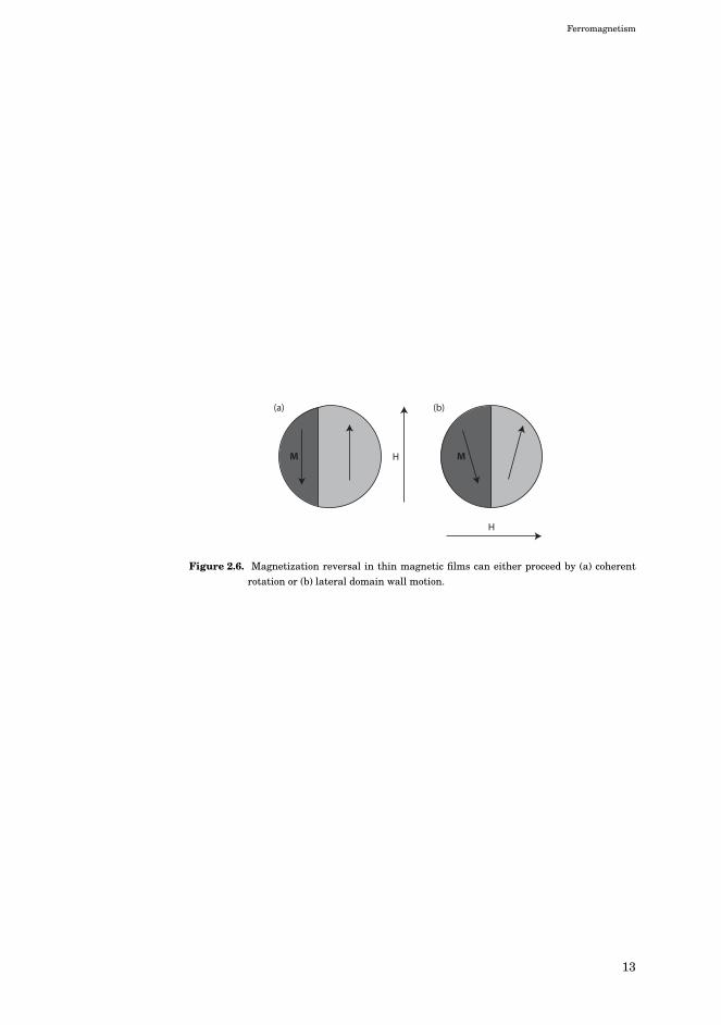
Figure 2.6. Magnetization reversal in thin magnetic films can either proceed by (a) coherentrotation or (b) lateral domain wall motion.
13

Ferromagnetism
14
3. Ferroelectricity
Ferroelectric materials exhibit a spontaneous electric polarization, which can
be switched using an external electric field. This is analogous to the magneti-
zation and magnetization reversal in an applied magnetic field, which occur in
ferromagnetic materials. Unlike ferromagnetism, ferroelectricity is connected
to the structural properties of a material and not an intrinsic property of an
atom. The mechanisms that give rise to ferroelectricity are order-disorder (e.g.
KH2PO4) [30] and displacements of ions (e.g BaTiO3) [31, 32]. A ferroelectric
material is characterized by a hysteresis loop, called a P −E loop. Similar to
the M−H loop of a ferromagnet shown in Figure 2.4, in a P −E loop the polar-
ization P replaces M and an external electric field E replaces H. The electric
polarization P can be reversed by a sufficiently large external electric field Ec.
Ferroelectric materials loose their spontaneous polarization and become para-
electric above a critical Curie temperature, Tc.
All ferroelectric materials also exhibit pyroelectricity, piezoelectricity and some-
times ferroelasticity. Pyroelectricity is a change in the polarization due to a
change in temperature, ferroelasticity is the presence of a spontaneous strain,
and piezoelectricity is the accumulation of charges due to an applied strain on
the material. The polarization of a piezoelectric material can be written as [33]
P = Zd+Eχ, (3.1)
where Z is the stress, d is the piezoelectric constant, E is the electric field
and χ is the dielectric susceptibility.
The ferroelectric material used throughout this thesis is Barium Titanate,
which will be discussed in more detail in the following Sections.
15
Ferroelectricity
a b
c
Titanium
Barium
Oxygen
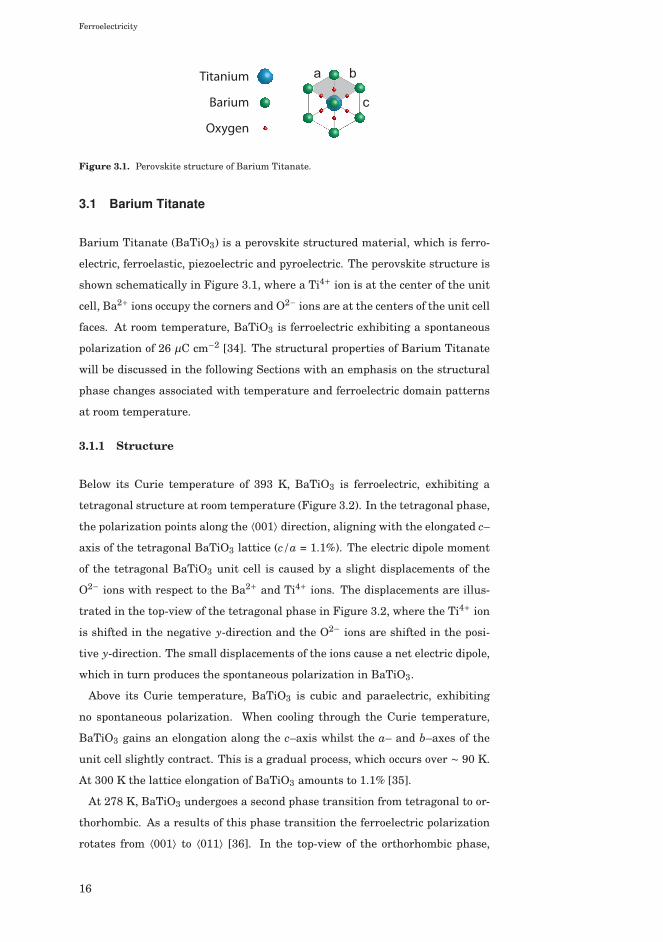
Figure 3.1. Perovskite structure of Barium Titanate.
3.1 Barium Titanate
Barium Titanate (BaTiO3) is a perovskite structured material, which is ferro-
electric, ferroelastic, piezoelectric and pyroelectric. The perovskite structure is
shown schematically in Figure 3.1, where a Ti4+ ion is at the center of the unit
cell, Ba2+ ions occupy the corners and O2− ions are at the centers of the unit cell
faces. At room temperature, BaTiO3 is ferroelectric exhibiting a spontaneous
polarization of 26 μC cm−2 [34]. The structural properties of Barium Titanate
will be discussed in the following Sections with an emphasis on the structural
phase changes associated with temperature and ferroelectric domain patterns
at room temperature.
3.1.1 Structure
Below its Curie temperature of 393 K, BaTiO3 is ferroelectric, exhibiting a
tetragonal structure at room temperature (Figure 3.2). In the tetragonal phase,
the polarization points along the ⟨001⟩ direction, aligning with the elongated c–
axis of the tetragonal BaTiO3 lattice (c/a = 1.1%). The electric dipole moment
of the tetragonal BaTiO3 unit cell is caused by a slight displacements of the
O2− ions with respect to the Ba2+ and Ti4+ ions. The displacements are illus-
trated in the top-view of the tetragonal phase in Figure 3.2, where the Ti4+ ion
is shifted in the negative y-direction and the O2− ions are shifted in the posi-
tive y-direction. The small displacements of the ions cause a net electric dipole,
which in turn produces the spontaneous polarization in BaTiO3.
Above its Curie temperature, BaTiO3 is cubic and paraelectric, exhibiting
no spontaneous polarization. When cooling through the Curie temperature,
BaTiO3 gains an elongation along the c–axis whilst the a– and b–axes of the
unit cell slightly contract. This is a gradual process, which occurs over ∼ 90 K.
At 300 K the lattice elongation of BaTiO3 amounts to 1.1% [35].
At 278 K, BaTiO3 undergoes a second phase transition from tetragonal to or-
thorhombic. As a results of this phase transition the ferroelectric polarization
rotates from ⟨001⟩ to ⟨011⟩ [36]. In the top-view of the orthorhombic phase,
16
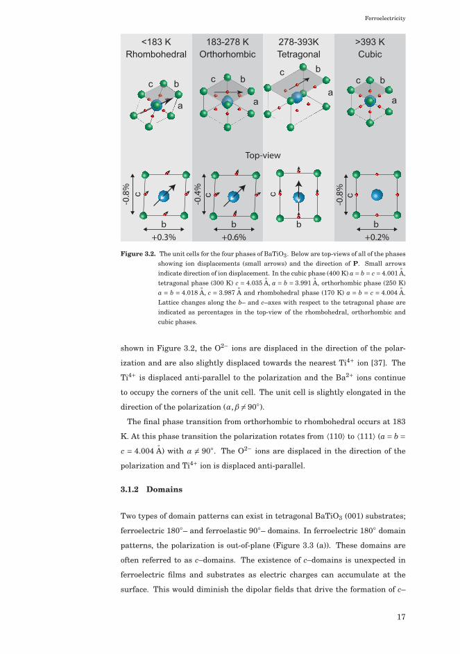
Ferroelectricity
aa
bb c
a
bcc
a
b
c
c
c c c
Rhombohedral<183 K
Orthorhombic183-278 K
Tetragonal278-393K
Cubic>393 K
Top-view
+0.2%+0.6%
-0.4
%
-0.8
%
+0.3%
-0.8
%
b b b b
Figure 3.2. The unit cells for the four phases of BaTiO3. Below are top-views of all of the phasesshowing ion displacements (small arrows) and the direction of P. Small arrowsindicate direction of ion displacement. In the cubic phase (400 K) a = b = c = 4.001
◦A,
tetragonal phase (300 K) c = 4.035◦A, a = b = 3.991
◦A, orthorhombic phase (250 K)
a = b = 4.018◦A, c = 3.987
◦A and rhombohedral phase (170 K) a = b = c = 4.004
◦A.
Lattice changes along the b– and c–axes with respect to the tetragonal phase areindicated as percentages in the top-view of the rhombohedral, orthorhombic andcubic phases.
shown in Figure 3.2, the O2− ions are displaced in the direction of the polar-
ization and are also slightly displaced towards the nearest Ti4+ ion [37]. The
Ti4+ is displaced anti-parallel to the polarization and the Ba2+ ions continue
to occupy the corners of the unit cell. The unit cell is slightly elongated in the
direction of the polarization (α,β �= 90◦).
The final phase transition from orthorhombic to rhombohedral occurs at 183
K. At this phase transition the polarization rotates from ⟨110⟩ to ⟨111⟩ (a = b =c = 4.004
◦A) with α �= 90◦. The O2− ions are displaced in the direction of the
polarization and Ti4+ ion is displaced anti-parallel.
3.1.2 Domains
Two types of domain patterns can exist in tetragonal BaTiO3 (001) substrates;
ferroelectric 180◦– and ferroelastic 90◦– domains. In ferroelectric 180◦ domain
patterns, the polarization is out-of-plane (Figure 3.3 (a)). These domains are
often referred to as c–domains. The existence of c–domains is unexpected in
ferroelectric films and substrates as electric charges can accumulate at the
surface. This would diminish the dipolar fields that drive the formation of c–
17
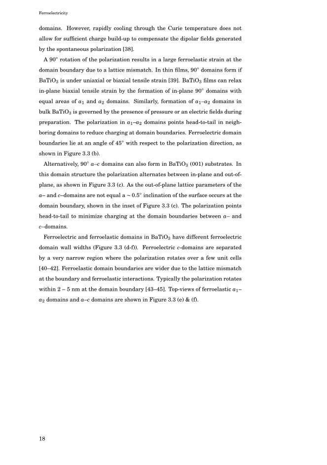
Ferroelectricity
domains. However, rapidly cooling through the Curie temperature does not
allow for sufficient charge build-up to compensate the dipolar fields generated
by the spontaneous polarization [38].
A 90◦ rotation of the polarization results in a large ferroelastic strain at the
domain boundary due to a lattice mismatch. In thin films, 90◦ domains form if
BaTiO3 is under uniaxial or biaxial tensile strain [39]. BaTiO3 films can relax
in-plane biaxial tensile strain by the formation of in-plane 90◦ domains with
equal areas of a1 and a2 domains. Similarly, formation of a1–a2 domains in
bulk BaTiO3 is governed by the presence of pressure or an electric fields during
preparation. The polarization in a1–a2 domains points head-to-tail in neigh-
boring domains to reduce charging at domain boundaries. Ferroelectric domain
boundaries lie at an angle of 45◦ with respect to the polarization direction, as
shown in Figure 3.3 (b).
Alternatively, 90◦ a–c domains can also form in BaTiO3 (001) substrates. In
this domain structure the polarization alternates between in-plane and out-of-
plane, as shown in Figure 3.3 (c). As the out-of-plane lattice parameters of the
a– and c–domains are not equal a ∼ 0.5◦ inclination of the surface occurs at the
domain boundary, shown in the inset of Figure 3.3 (c). The polarization points
head-to-tail to minimize charging at the domain boundaries between a– and
c–domains.
Ferroelectric and ferroelastic domains in BaTiO3 have different ferroelectric
domain wall widths (Figure 3.3 (d-f)). Ferroelectric c-domains are separated
by a very narrow region where the polarization rotates over a few unit cells
[40–42]. Ferroelastic domain boundaries are wider due to the lattice mismatch
at the boundary and ferroelastic interactions. Typically the polarization rotates
within 2 – 5 nm at the domain boundary [43–45]. Top-views of ferroelastic a1–
a2 domains and a–c domains are shown in Figure 3.3 (e) & (f).
18
Ferroelectricity
Domain boundary
(a)
c-do
mai
n
c-do
mai
n
~0.5º(c)
c-do
mai
n
a-do
mai
n
(b)
(d)
(f )
(e)
a 2-d
omai
n
a 1-d
omai
n
+1.1%
+1.1
%
+1.1%
Figure 3.3. Domain patterns found in BaTiO3 (001): c–domains are shown in (a), a1–a2 do-mains in (b) and a–c domains in (c) with an inset showing angle between domainsat the surface. The structural changes at ferroelectric/ferroelastic domain bound-aries are illustrated in (d)–(f).
19

Ferroelectricity
20

4. Multiferroics
Multiferroic materials exhibit more than one ferroic order parameter (mag-
netic, electric aor elastic). Coupling between different ferroic order parameters
holds potential for electric field controlled magnetic memory, 4-state logic and
magnetoelectric sensors. This has contributed to an increased research interest
in multiferroic materials in recent years [46–52].
Multiferroics exist in two forms; single-phase multiferroics and multiferroic
heterostructures. Single-phase multiferroics intrinsically exhibit more than
one ferroic order parameter. Typically either one or both of the order parame-
ters are weak and only arise at low temperatures. Multiferroic heterostructures
are artificially created by coupling two ferroic materials through an interface.
A brief discussion of the different multiferroic systems with an emphasis on
electric-field-control of magnetism is presented here.
4.1 Single-phase multiferroics
Two categories of single-phase multiferroics exist; type I (ferroelectric and mag-
netic orders originate from independent phenomena) and type II (ferroelectric-
ity is directly linked to the magnetic order). Type I multiferroics (e.g. YMnO3)
seldom have both magnetic and ferroelectric ordering temperatures above room
temperature. The ordering temperatures for ferroelectricity and magnetism are
different as the ferroelectric and magnetic moments arise from different phe-
nomenon. This also leads to weak coupling between the ferroic states. The
magnetic order originates from an imbalance between electron spin states and
spin-orbit coupling. Ferroelectricity can occur due to lone pairs (ordering of
polarizable 6s electron pairs), charge ordering (in equivalence of ion sites and
bonds) or ion displacements.
BiFeO3 is a commonly studied Type I single phase multiferroic. It is both
antiferromagnetic and ferroelectric and it has been shown that the Curie tem-
21

Multiferroics
perature of both the ferroelectric and anti-ferromagnetic phases are above room
temperature [53]. Whilst BiFeO3 has a large ferroelectric polarization of 90 μC
cm−2 [53, 54], it is generally accepted that BiFeO3 exhibits a weak magnetic
moment of 0.05 μB/Fe [55–57]. Zhao et al demonstrated electric-field-control
of antiferromagnetic domains in BiFeO3 through coupling of antiferromagnetic
and ferroelectric domains to the underlying ferroelastic domain structure [58].
In type II multiferroics (e.g. TbMnO3, Ca3CoMnO6) the ferroelectric polar-
ization directly originates from particular types of magnetic spiral or collinear
magnetic structures. In both cases, magnetic interactions give rise to a net
polarization at low temperatures, which directly couples the ferroic order pa-
rameters [59,60]. The coupling between the ferroic order parameters has been
largely limited to magnetic field control of ferroelectric polarization [61].
4.2 Multiferroic heterostructures
Using heterostructures to create artificial multiferroics allows for materials to
be chosen for specific purposes requiring strong coupling, high ordering temper-
atures or large ferroic order parameters [51,52]. In addition to the wide choice
of ferroelectric and magnetic materials available, multiferroic heterostructures
can also be tweaked by modifying the crystal orientation, lattice strain, elec-
tronic state, domain pattern and defect structure at the interface between the
ferroic materials.
One method of coupling ferroic orders in multiferroic heterostructures is thro-
ugh nanopillar structures. Magnetic nanopillars in a ferroelectric medium are
typically produced by self-assembly during co-deposition of magnetic and fer-
roelectric materials. This has been realized experimentally by co-deposition
of ferroelectric perovskites (BaTiO3, PbTiO3) and magnetic spinels (CoFe2O4,
NiFe2O4, and Fe3O4) [62–71] at high temperatures. The magnetic materials
organize into crystalline pillars during deposition. An advantage here is the
large contact surface area between the ferroelectric and magnetic materials
and reduced mechanical clamping by the substrate [48]. Zavaliche et al demon-
strated electric-field-induced magnetization switching in CoFe2O4 nanopillars
in a BiFeO3 medium [64]. As nanopillar structures heavily depend on self-
assembly they are limited by the choice of materials leading to a restricted
design and control of such structures.
Alternatively, the fabrication of thin film multiferroic heterostructures does
not depend on self-assembly, therefore a larger variety of materials are avail-
able. Also, thin film heterostructures are appealing because the layered geom-
22
Multiferroics
etry closely mimics the architecture of most practical devices. Three different
mechanisms can drive electric-field-induced changes, namely charge modula-
tion, exchange interaction and strain transfer.
4.2.1 Charge modulation
The electric field generated by a spontaneous polarization at the interface be-
tween a ferroelectric and thin magnetic film can modify the magnetization
of the magnetic material. Screening of interface charges by depletion or ac-
cumulation of charge carriers at the interface affects the magnetic moment,
anisotropy or magnetic ordering state. These effects have been demonstrated
in metallic ferromagnets, magnetic oxides and dilute magnetic semiconduc-
tors [72–84]. Alternatively, atom displacements at the interface can affect the
overlap between atomic orbitals altering the magnetic properties. For example,
magnetic moment alterations have been demonstrate through ab initio calcu-
lations at a Fe/BaTiO3 interface [72]. Here, the hybridization of Fe and Ti 3d-
orbitals cause a charge redistribution of majority and minority spins depending
on the Fe–Ti bond length. Hence, electric-field-control of magnetization can be
realized at a TiO2 terminated BaTiO3/Fe interface, since the Fe–Ti bond length
depends on the polarization direction of the BaTiO3. Similar effects have been
calculated for Co2MnSi/BaTiO3 [85] and Fe3O4/BaTiO3 interfaces [75]. Hy-
bridization effects, which are strictly limited to the magnetic-ferroelectric in-
terface have also been experimentally measured in tunnel junctions with a fer-
roelectric barrier [86–88].
4.2.2 Exchange interaction
Exchange interactions can couple single phase multiferroics that are both fer-
roelectric and antiferromagnetic (e.g. YMnO3, LuMnO3, BiFeO3) to an adjacent
magnetic film [89–97]. Coupling of magnetic domains to ferroelectric domains
in CoFe/BiFeO3 heterostructures has been demonstrated [91, 94, 97]. In these
heterostructures, an easy magnetic anisotropy axis was created in the CoFe film
parallel to the canted magnetic moment in the BiFeO3. Since the magnetic mo-
ment in BiFeO3 is directly linked to the ferroelectric polarization a correlation
between magnetic and ferroelectric domains could be obtained. Furthermore,
ferroelectric domains could be rewritten by applying an electric field, which
resulted in the rearrangement of the magnetic domains.
23
Multiferroics
4.2.3 Strain transfer
Electric field control of magnetization in multiferroic heterostructures can also
be realized by elastical coupling between a magnetic thin film and a ferro-
electric or piezoelectric substrate. Here, the lattice strain of the ferroelect-
ric/piezoelectric is modified with an electric field. Through interfacial strain
transfer this leads to a controllable strain in the adjacent magnetic film. Elec-
tric field control of the magnetoelastic anisotropy in the magnetic film is then
obtained via inverse magnetostriction. The behavior of strain-controlled het-
erostructures depends on the competition between magnetoelastic and magne-
tocrystalline anisotropies, and magnetostatic and exchange interactions.
The nature of strain transfer from a piezoelectric or ferroelectric material are
different. Piezoelectric materials produce a linear strain response in an applied
electric field, which leads to a linear magnetic response [51, 98]. Due to the
linear and reversible evolution of strain, the original strain state is restored
when the electric field is removed. Therefore, piezostrain-induced magnetic
changes are mostly volatile.
The electric-field-induced strain in a piezoelectric material can be either uni-
axial or biaxial depending on the crystal orientation. (1− x) Pb(Zn1/3Nb2/3)O3−x PbTiO3 (PZN-PT) and (1−x) Pb(Mn1/3Nb2/3)O3 −xPbTiO3 (PMN-PT) are com-
mon relaxor ferroelectric that exhibits a butterfly shaped piezostrain curve.
The crystallographic orientation of these substrates can be used to select the
type of strain it provides: (001) oriented crystals provide a biaxial in-plane
strain response whereas (011) oriented substrates provide an uniaxial strain
response in an out-of-plane electric field. PMN-PT has been utilized in tuning
the magnetic properties of manganite [98–101], ferrite [102–106], and metal-
lic magnetic films [107–109], and also in altering the electrical resistance of
magnetic oxides [99, 101, 105, 110–113]. The uniaxial strain provided by (011)
PZN-PT has been used to demonstrate electric-field-tuning of the ferromagne-
tic resonance (FMR) in magnetic FeGaB films. By adjusting the electric field
strength the strength of the magnetoelastic anisotropy was tuned, which no-
tably changed the measured FMR frequency due to the large magnetostriction
of FeGaB [114–118]. The original FMR frequency is restored when the electric
field is removed.
Tiercelin et al demonstrated a bistable magnetization state in zero applied
electric field in an TbCo2/FeCo substrate coupled to a piezoelectric (011) PZT
stack [119]. By applying a constant external magnetic field perpendicular to a
growth-induced uniaxial anisotropy axis, two stable magnetization states were
24
Multiferroics
created 90◦ apart in the TbCo2/FeCo stack. The strong fourfold magnetocrys-
talline anisotropy of epitaxial FeGa films has also been used to demonstrate
non-volatile 90◦ magnetic switching in an applied electric field [120]. This re-
sulted in a 90◦ switch of the magnetization state by applying either a posi-
tive or negative out-of-plane electric field pulse. Another mechanism that can
provide deterministic electric-field-control of magnetic switching is exchange
bias. Liu et al. have demonstrated that piezoelectric strain transfer from
PZN-PT (011) substrates to FeMn/NiFe/FeGaB multilayers lead to near 180◦
rotation of the magnetization in an applied electric field [118]. Other propos-
als involve the use of bistable piezostrains of a partially poled (011) piezoelec-
tric layer [121, 122]. Experimentally it has been shown that bistable in-plane
piezostrains can be used for permanent magnetization switching in polycrys-
talline Ni films on (011) PMN-PT substrates [108]. Also, the hysteretic strain–
voltage dependence of piezoelectric actuators has been used to demonstrate re-
versible electric field controlled switching of the remanent magnetization in
polycrystalline Ni films [123].
Polarization reversal in a ferroelectric material is hysteretic. If the reversal
process involves the nucleation and growth of ferroelastic domains, i.e. do-
mains that are separated by non-180◦ domain walls, the lattice strain changes
abruptly during ferroelectric switching. A hysteretic strain–voltage curve is
obtained when the ferroelectric polarization rotates by less than 180◦, which
can be used to alter the magnetic properties of an adjacent magnetic film in
a non-volatile manner. The maximum transferable strain from a ferroelectric
substrate to a magnetic film depends on the ferroelectric material. As an exam-
ple, PbTiO3 and BaTiO3 are both ferroelectric materials, but their tetragonal
lattice elongations provide very different uniaxial strains of 6.4% and 1.1% re-
spectively. Moreover, the strength of the magnetoelastic anisotropy induced by
the ferroelectric substrate depends on the efficiency of strain transfer and the
magnetoelastic properties of the magnetic film. Additionally, the symmetry of
the induced magnetoelastic anisotropy depends on ferroelectric crystal struc-
ture, its orientation, and the direction of the polarization. Importantly, strain
transfer from ferroelastic domains is laterally modulated. The induced magne-
toelastic anisotropy in an adjacent magnetic film depends on the polarization
direction in the underlying ferroelectric domain, which paves the way towards
robust coupling between the orientation of local magnetoelastic anisotropy and
the direction of ferroelectric polarization. The local characteristics of the strain
transfer allows for the imprinting of ferroelectric domains into magnetic films
and strong pinning of magnetic domain walls on top of ferroelectric domain
25

Multiferroics
boundaries.
Structural phase transitions of BaTiO3 substrates have been used to demon-
strate strain coupling between a ferroelectric substrate and a magnetic film.
The BaTiO3 lattice undergoes changes from cubic to tetragonal at 393 K, tetrag-
onal to orthogonal at 278 K and orthogonal to rhombohedral at 183 K [36].
These lattice transitions alter the strain state and thereby the magnetoelas-
tic anisotropy of the magnetic film as indicated by abrupt jumps in magneti-
zation. Macroscopic results have been obtained for La1-xSrxMnO3 [124, 125],
Fe3O4 [126–128], Fe [129–134] and Sr2CrReO6 [135].
Electric-field-control of magnetism using BaTiO3 substrates has been demon-
strated in various magnetic films [129,131,133,136,137]. Eerenstein et al have
demonstrated electric-field-control of magnetization in La1-xSrxMnO3 [125]. Ap-
plying an electric field in the different structural phases of BaTiO3 resulted
in abrupt changes to the magnetization as measured by VSM. Similar mag-
netic responses in an applied electric field have also been observed in Fe films
[129,134].
The macroscopic measurements discussed above do not provide information
on the magnetic response on different ferroelectric domains. Due to the local
strain transfer from ferroelastic domains, the change in magnetization varies
from one domain to the other. Moreover, a variety of ferroelectric domain trans-
formations can occur at the BaTiO3 phase transitions, which complicates the
interpretation of macroscopic data. The work presented in this thesis focuses
on the imaging and measuring of ferroelectric–magnetic domain interactions
using optical polarization microscopy. It is shown that these interactions result
in domain pattern transfer from the ferroelectric substrates to the magnetic
films. The magnetic domains are pinned on top of their ferroelectric counter-
parts, which enables electric-field-control of magnetic domain wall motion and
local magnetization rotation in zero applied magnetic field.
26

5. Experimental Methods and Modeling
The ferroelectric substrate used throughout the study presented in this thesis is
BaTiO3, and the magnetic films grown on top are amorphous CoFeB, polycrys-
talline CoFe and epitaxial Fe. This chapter summarizes the growth methods
and deposition conditions for each film material and sample characterization
methods used.
5.1 Thin film growth
Three different strain-driven multiferroic heterostructure systems are investi-
gated in this work, all of which utilize inverse magnetostriction. BaTiO3 was
chosen as the ferroelectric substrate material as it possesses a large c/a ra-
tio of 1.1%. Ferromagnetic Co60Fe40 (CoFe), Fe and Co40Fe40B20 (CoFeB) were
selected as film materials: CoFe and CoFeB were chosen for their large magne-
tostrictions (λs) of 6.8 × 10⁻⁵ [138] and 3.5 × 10⁻⁵ [6] respectively to maximize
the magnetoelastic anisotropy. Fe was selected because of its lattice-match with
the BaTiO3 substrate allowing for epitaxial growth of Fe on to BaTiO3 sub-
strates.
The CoFe films were grown onto 10 mm × 10 mm × 0.5 mm BaTiO3 (001)
substrates with a1 − a2 domain patterns at room temperature using electron
beam evaporation (Section 5.1.1). These films had a polycrystalline texture,
which reduces the magnetocrystalline anisotropy. Moreover, the composition of
60% Co and 40% Fe exhibits a low magnetocrystalline anisotropy [139]. Due to
the minimal magnetocrystalline anisotropy the strain-induced magnetoelastic
anisotropy fully dominates the magnetic properties of CoFe/BaTiO3 (001)
To study the competition between magnetocrystalline and anisotropy in multi-
ferroic heterostructures epitaxial, 10 nm and 20 nm thick Fe films were grown
using molecular beam epitaxy (Section 5.1.2) onto 5 mm × 5 mm × 0.5 mm
BaTiO3 (001) substrates containing an a− c domain structure. A requirement
27
Experimental Methods and Modeling
HCrucible
Substrate
Gun
e-
Targetmaterial
Target atoms Quartz crystal
+
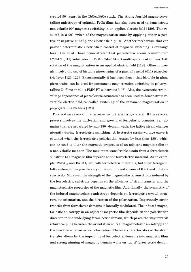
Figure 5.1. Electron beam evaporation utilizes a beam of electrons to heat a target material ina grounded crucible causing the material to sublime and condense on to a substrateplaced opposite of the crucible.
for epitaxial film growth is a good lattice match between the substrate and film.
Fe has a lattice parameter of 2.867 Å [6], which is a good match with BaTiO3 if
Fe[110] ‖ BTO[100] (aFe [110] = 4.059 Å cBTO=4.035 Å aBTO=3.991 Å). The Fe unit
cell is compressed by 0.6% along the c–axis and 1.6% along the a–axis of the
BaTiO3 substrate.
CoFeB films were grown using magnetron sputtering (Section 5.1.3) onto 5
mm × 5 mm × 0.5 mm BaTiO3 substrates with (011) oriented surfaces consist-
ing of so-called a–b domains. The lateral uniaxial strains provided by the a and
b domains are 1.1% and 0.55% respectively. The CoFeB film was grown as a
wedge to study competition between magnetoelastic anisotropy and magneto-
static interactions between neighboring magnetic domains with increasing film
thickness. The amorphous CoFeB films exhibit a negligible magnetocrystalline
anisotropy.
5.1.1 Electron beam evaporation
Electron beam (e-beam) evaporation is a thin film deposition method conducted
under vacuum conditions. A beam of electrons is created by thermionic emis-
sion from a W filament and directed towards a target material using a magnetic
field. Figure 5.1 schematically illustrates a beam of electrons (e−) from a W fil-
ament accelerated through a positively charged slit. The magnetic field, H, is
perpendicular to the beam causing the electrons to adopt a trajectory towards
the crucible. The electrons bombard the target material inside the crucible
causing it to vaporize and condense onto the substrate placed opposite to the
28

Experimental Methods and Modeling
Substrate
Effusion cellTarget material
Heater
Figure 5.2. Schematic illustration of molecular beam epitaxy.
crucible. To prevent charging, the target and crucible both have to be conduct-
ing and grounded [140].
The deposition rate of electron beam evaporation is controlled by adjusting
the current density of the electron beam. A quartz crystal microbalance is used
to monitor the film thickness. A quartz crystal is oscillated at its resonance
frequency, which depends on its surface properties. As the target material con-
denses onto the surface of the oscillating quartz crystal the resonance frequency
changes, which is used to determine the thickness if the density and charge
density of the film are known [141].
The samples prepared for this thesis by e-beam evaporation consisted of 15 –
20 nm CoFe films with a 3 nm Au capping layer to prevent oxidation. The films
were grown at room temperature. The base pressure of the chamber before film
deposition was ∼10−7 mbar and a liquid N2 trap was used during outgassing
of CoFe. A deposition rate of 0.1 – 0.2 nm/s was set before growth was ini-
tialized by opening a shutter plate above the crucible. The growth of smooth
polycrystalline films was confirmed by x-ray diffraction and transmission elec-
tron microscopy.
29
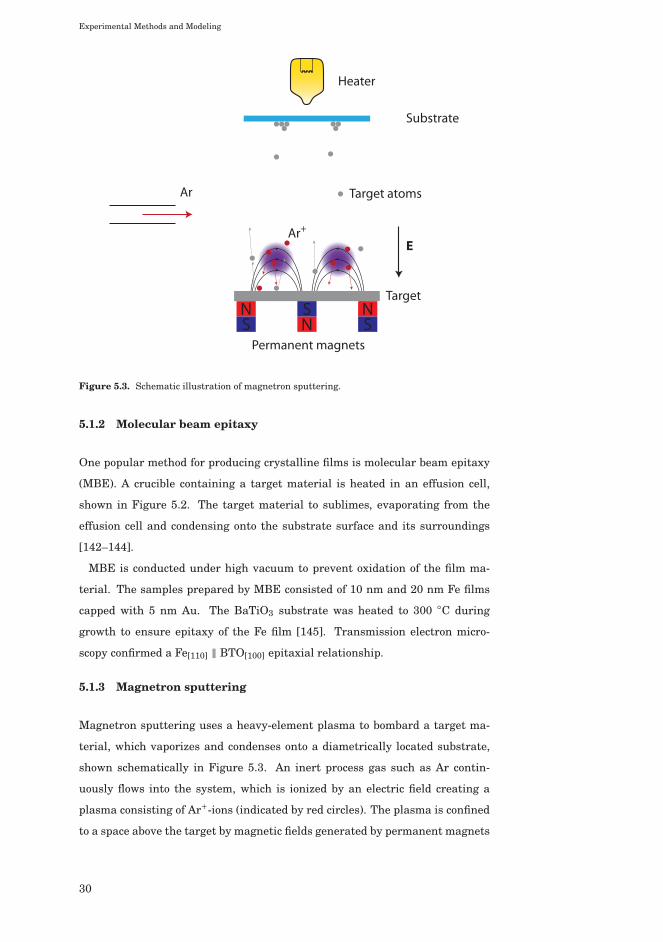
Experimental Methods and Modeling
EAr+
Ar
Heater
Substrate
Target
Target atoms
Permanent magnets
Figure 5.3. Schematic illustration of magnetron sputtering.
5.1.2 Molecular beam epitaxy
One popular method for producing crystalline films is molecular beam epitaxy
(MBE). A crucible containing a target material is heated in an effusion cell,
shown in Figure 5.2. The target material to sublimes, evaporating from the
effusion cell and condensing onto the substrate surface and its surroundings
[142–144].
MBE is conducted under high vacuum to prevent oxidation of the film ma-
terial. The samples prepared by MBE consisted of 10 nm and 20 nm Fe films
capped with 5 nm Au. The BaTiO3 substrate was heated to 300 ◦C during
growth to ensure epitaxy of the Fe film [145]. Transmission electron micro-
scopy confirmed a Fe[110] ‖ BTO[100] epitaxial relationship.
5.1.3 Magnetron sputtering
Magnetron sputtering uses a heavy-element plasma to bombard a target ma-
terial, which vaporizes and condenses onto a diametrically located substrate,
shown schematically in Figure 5.3. An inert process gas such as Ar contin-
uously flows into the system, which is ionized by an electric field creating a
plasma consisting of Ar+-ions (indicated by red circles). The plasma is confined
to a space above the target by magnetic fields generated by permanent magnets
30

Experimental Methods and Modeling
underneath the target. If a ferromagnetic target is used the magnets in the gun
have to be strong enough to overcome dipolar fields generated by the target. Ap-
plying a negative DC voltage on to the target material accelerates the Ar+-ions
towards the target (indicated by red arrows) causing target atoms (gray circles)
to be knocked out. The vaporized target atoms form a plume, travelling thro-
ugh the atoms and ions in the chamber atmosphere performing a random-walk
before condensing on to the substrate and chamber walls. Reactive gases such
as O2 can also be incorporated into the process gas to create oxides and other
material mixtures [146–149].
A plasma can be maintained during sputtering at low pressures (∼ 10−4 mbar)
because the bombardment process continuously ionizes Ar atoms, which feed
the plasma. To form the plasma a critical voltage, Vcrit, is required to initiate
the plasma formation process.
Two parameters control the rate of growth of the thin film; the process gas
pressure and the voltage applied to the target. Using a higher process gas
pressure increases the likelihood of ionization events which in turn decreases
Vcrit. However, an increase in pressure also decreases the mean free path of
target atoms decreasing the growth rate. An increase in the voltage above
Vcrit increases growth rate as the Ar+-ions gain more energy, which increases
evaporation events on the target surface.
A mechanized shutter is used to control the exposure of the substrate to the
vaporized target material. The shutter is closed during an initialization period
where the production of the plasma is started and impurities on the target sur-
face are evaporated. Once the initialization is complete the rate of evaporation
is linear with time and therefore the film thickness is controlled by setting the
total sputter time. The growth rate is calibrated by measuring the film thick-
ness of a control sample using small-angle x-ray diffraction.
The CoFeB and Au targets used for sample preparation by magnetron sput-
tering were 2 inches in diameter with the target–substrate distance ∼10 cm.
The base pressure of the system before sputtering was ∼10−7 mbar. Ar was
used as the process gas. An Ar flow of 30 sccm was used during deposition,
which resulted in an Ar sputtering pressure of 6 × 10⁻³ mbar. The CoFeB film
was grown as a wedge film from 0 nm to 110 nm thickness using a motorized
shadow mask system, as schematically shown in Figure 5.4. During growth
the mask was moved towards the direction indicated by the white arrow. This
resulted in a linear increase of the CoFeB film thickness. The distance between
the mask and substrate was ∼3 mm. The power applied to the target was 50 W
and 30 W, which resulted in growth rates of 0.16 nm/s and 0.2 nm/s for CoFeB
31
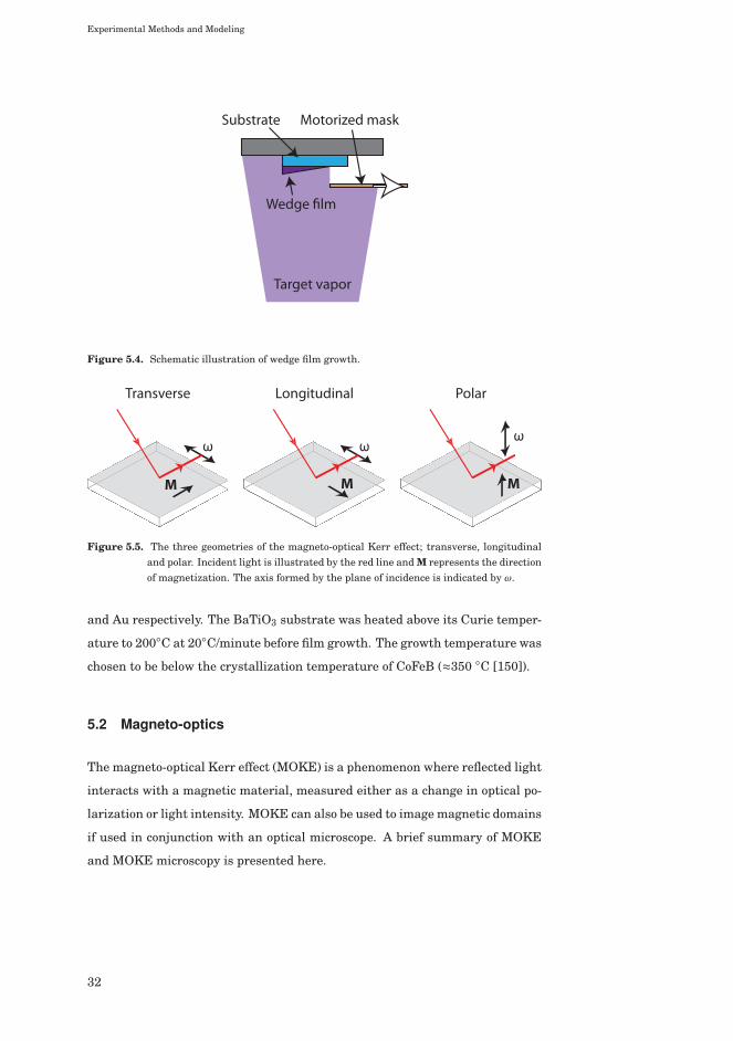
Experimental Methods and Modeling
Substrate
Target vapor
Wedge film
Motorized mask
Figure 5.4. Schematic illustration of wedge film growth.
Transverse Longitudinal Polar
M M M
ω ωω
Figure 5.5. The three geometries of the magneto-optical Kerr effect; transverse, longitudinaland polar. Incident light is illustrated by the red line and M represents the directionof magnetization. The axis formed by the plane of incidence is indicated by ω.
and Au respectively. The BaTiO3 substrate was heated above its Curie temper-
ature to 200◦C at 20◦C/minute before film growth. The growth temperature was
chosen to be below the crystallization temperature of CoFeB (≈350 ◦C [150]).
5.2 Magneto-optics
The magneto-optical Kerr effect (MOKE) is a phenomenon where reflected light
interacts with a magnetic material, measured either as a change in optical po-
larization or light intensity. MOKE can also be used to image magnetic domains
if used in conjunction with an optical microscope. A brief summary of MOKE
and MOKE microscopy is presented here.
32
Experimental Methods and Modeling
5.2.1 Magneto-optical Kerr effect
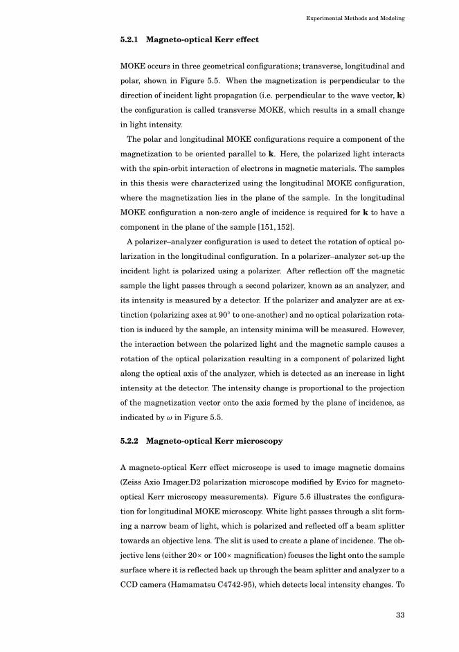
MOKE occurs in three geometrical configurations; transverse, longitudinal and
polar, shown in Figure 5.5. When the magnetization is perpendicular to the
direction of incident light propagation (i.e. perpendicular to the wave vector, k)
the configuration is called transverse MOKE, which results in a small change
in light intensity.
The polar and longitudinal MOKE configurations require a component of the
magnetization to be oriented parallel to k. Here, the polarized light interacts
with the spin-orbit interaction of electrons in magnetic materials. The samples
in this thesis were characterized using the longitudinal MOKE configuration,
where the magnetization lies in the plane of the sample. In the longitudinal
MOKE configuration a non-zero angle of incidence is required for k to have a
component in the plane of the sample [151,152].
A polarizer–analyzer configuration is used to detect the rotation of optical po-
larization in the longitudinal configuration. In a polarizer–analyzer set-up the
incident light is polarized using a polarizer. After reflection off the magnetic
sample the light passes through a second polarizer, known as an analyzer, and
its intensity is measured by a detector. If the polarizer and analyzer are at ex-
tinction (polarizing axes at 90◦ to one-another) and no optical polarization rota-
tion is induced by the sample, an intensity minima will be measured. However,
the interaction between the polarized light and the magnetic sample causes a
rotation of the optical polarization resulting in a component of polarized light
along the optical axis of the analyzer, which is detected as an increase in light
intensity at the detector. The intensity change is proportional to the projection
of the magnetization vector onto the axis formed by the plane of incidence, as
indicated by ω in Figure 5.5.
5.2.2 Magneto-optical Kerr microscopy
A magneto-optical Kerr effect microscope is used to image magnetic domains
(Zeiss Axio Imager.D2 polarization microscope modified by Evico for magneto-
optical Kerr microscopy measurements). Figure 5.6 illustrates the configura-
tion for longitudinal MOKE microscopy. White light passes through a slit form-
ing a narrow beam of light, which is polarized and reflected off a beam splitter
towards an objective lens. The slit is used to create a plane of incidence. The ob-
jective lens (either 20× or 100× magnification) focuses the light onto the sample
surface where it is reflected back up through the beam splitter and analyzer to a
CCD camera (Hamamatsu C4742-95), which detects local intensity changes. To
33
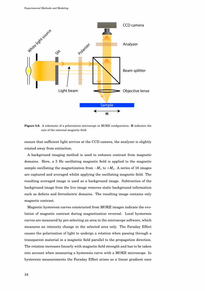
Experimental Methods and Modeling
White lig
ht source
Slit Polarizer
Beam splitter
Objective lense
Analyzer
CCD camera
Light beam
Sample
H
Figure 5.6. A schematic of a polarization microscope in MOKE configuration. H indicates theaxis of the external magnetic field.
ensure that sufficient light arrives at the CCD camera, the analyzer is slightly
rotated away from extinction.
A background imaging method is used to enhance contrast from magnetic
domains. Here, a 5 Hz oscillating magnetic field is applied to the magnetic
sample oscillating the magnetization from −Ms to +Ms. A series of 16 images
are captured and averaged whilst applying the oscillating magnetic field. The
resulting averaged image is used as a background image. Subtraction of the
background image from the live image removes static background information
such as defects and ferroelectric domains. The resulting image contains only
magnetic contrast.
Magnetic hysteresis curves constructed from MOKE images indicate the evo-
lution of magnetic contrast during magnetization reversal. Local hysteresis
curves are measured by pre-selecting an area in the microscope software, which
measures an intensity change in the selected area only. The Faraday Effect
causes the polarization of light to undergo a rotation when passing through a
transparent material in a magnetic field parallel to the propagation direction.
The rotation increases linearly with magnetic field strength and has to be taken
into account when measuring a hysteresis curve with a MOKE microscope. In
hysteresis measurements the Faraday Effect arises as a linear gradient once
34
Experimental Methods and Modeling
the magnetic sample has reached Ms. The hysteresis curves presented in this
thesis were obtained after subtraction of the Faraday Effect from the measure-
ment data.
Ferroelectric domains can be imaged using an optical polarization microscope
if the magnetic film on top of the BaTiO3 substrate is semi-transparent for
white light. Ferroelectric contrast originates from birefringence. Ferroelectric
domains can be isolated from magnetic contrast by saturating the magnetic
domains with an external magnetic field.
External magnetic fields are applied using an in-plane electromagnet. A
shunt resistor is used to measure the electric current flowing through the elec-
tromagnetic, which is used to determine the magnetic field strength. The mag-
netic field generated by the electromagnet is calibrated using a Hall sensor.
5.2.3 Electric field and temperature measurements
Electric field experiments were performed on the CoFe/BaTiO3 sample by ap-
plying an electric field perpendicular to the BaTiO3 substrate whilst imaging
ferroelectric and magnetic domains using the optical polarization microscope.
An electric field sample holder was designed for use in the microscope (Figure
5.7). The sample was attached to a metal back plate using silver paste, which
doubles as an electrode. The grounded metallic CoFe film on top of the sub-
strate acts as the second electrode. A positive voltage was applied to the back
plate. The voltage was ramped at 10 V/min to avoid substrate fracturing.
A continuous-flow liquid N2 microscope cryostat (Janis ST-500) was used for
temperature-control experiments (Figure 5.7). In this cryostat, thermal gel
provides a good thermal contact between the sample and sample mount. The
sample space is pumped down to 10−6 mbar during temperature-control exper-
iments. A 50 Ω heater in conjunction with a LakeShore temperature controller
is used to stabilize and control the sample temperature.
5.3 Magnetic modeling
A macrospin model and micromagnetic simulations were used to analyze do-
main pattern transfer and local magnetization reversal in multiferroic het-
erostructures. In the macrospin model the energy of two neighboring magnetic
stripe domains are minimized in an iterative fashion. The orientation of the
magnetoelastic anisotropy is orthogonal in neighboring domains and domain
coupling is taken into account by magnetostatic and exchange energy terms.
35
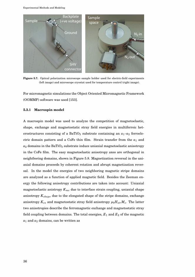
Experimental Methods and Modeling
SHVconnector
SampleSamplespace
Ground
Backplate(+ve voltage)
N2 in
N2 out
Figure 5.7. Optical polarization microscope sample holder used for electric-field experiments(left image) and microscope cryostat used for temperature control (right image).
For micromagnetic simulations the Object Oriented Micromagnetic Framework
(OOMMF) software was used [153].
5.3.1 Macrospin model
A macrospin model was used to analyze the competition of magnetoelastic,
shape, exchange and magnetostatic stray field energies in multiferroic het-
erostructures consisting of a BaTiO3 substrate containing an a1–a2 ferroele-
ctric domain pattern and a CoFe thin film. Strain transfer from the a1 and
a2 domains in the BaTiO3 substrate induce uniaxial magnetoelastic anisotropy
in the CoFe film. The easy magnetoelastic anisotropy axes are orthogonal in
neightboring domains, shown in Figure 5.8. Magnetization reversal in the uni-
axial domains proceeds by coherent rotation and abrupt magnetization rever-
sal. In the model the energies of two neighboring magnetic stripe domains
are analyzed as a function of applied magnetic field. Besides the Zeeman en-
ergy the following anisotropy contributions are taken into account: Uniaxial
magnetoelastic anistropy Kme due to interface strain coupling, uniaxial shape
anisotropy Kshape due to the elongated shape of the stripe domains, exchange
anisotropy Kex and magnetostatic stray field anisotropy μ0HstrMs. The latter
two anisotropies describe the ferromagnetic exchange and magnetostatic stray
field coupling between domains. The total energies, E1 and E2 of the magnetic
a1 and a2 domains, can be written as
36
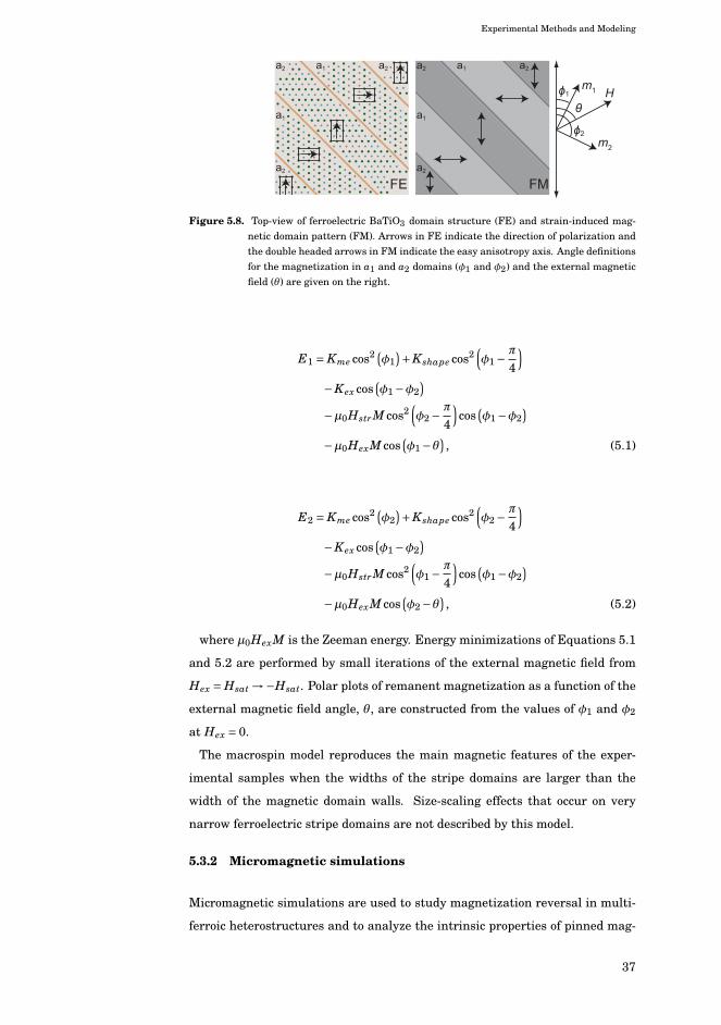
Experimental Methods and Modeling
Hm1
m2
��1
�2
a2a2
a2
a1
a1 a2a2
a2
a1
a1
FE FM
Figure 5.8. Top-view of ferroelectric BaTiO3 domain structure (FE) and strain-induced mag-netic domain pattern (FM). Arrows in FE indicate the direction of polarization andthe double headed arrows in FM indicate the easy anisotropy axis. Angle definitionsfor the magnetization in a1 and a2 domains (φ1 and φ2) and the external magneticfield (θ) are given on the right.
E1 = Kme cos2 (φ1
)+Kshape cos2(φ1 − π
4
)
−Kex cos(φ1 −φ2
)
−μ0HstrM cos2(φ2 − π
4
)cos
(φ1 −φ2
)
−μ0HexM cos(φ1 −θ
), (5.1)
E2 = Kme cos2 (φ2
)+Kshape cos2(φ2 − π
4
)
−Kex cos(φ1 −φ2
)
−μ0HstrM cos2(φ1 − π
4
)cos
(φ1 −φ2
)
−μ0HexM cos(φ2 −θ
), (5.2)
where μ0HexM is the Zeeman energy. Energy minimizations of Equations 5.1
and 5.2 are performed by small iterations of the external magnetic field from
Hex = Hsat →−Hsat. Polar plots of remanent magnetization as a function of the
external magnetic field angle, θ, are constructed from the values of φ1 and φ2
at Hex = 0.
The macrospin model reproduces the main magnetic features of the exper-
imental samples when the widths of the stripe domains are larger than the
width of the magnetic domain walls. Size-scaling effects that occur on very
narrow ferroelectric stripe domains are not described by this model.
5.3.2 Micromagnetic simulations
Micromagnetic simulations are used to study magnetization reversal in multi-
ferroic heterostructures and to analyze the intrinsic properties of pinned mag-
37

Experimental Methods and Modeling
-40 -20 0 20 40
-1
0
1
�0H (mT)
MR/M
S
a1a2
-40 -20 0 20 40
-1
0
1M
R/M
S
�0H (mT)
a1a2
(a) (b)
Figure 5.9. Measured (a) and simulated (b) magnetic hysteresis curves for the a1 and a2 do-mains of a CoFe film on top of BaTiO3.
netic domain walls. The OOMMF software uses a 3-D mesh of finite-size ele-
ments to locate local minima in the energy landscape through direct minimiza-
tion techniques during magnetization reversal in an external magnetic field. At
every step of the external magnetic field OOMMF produces a matrix containing
3-D spin information of each individual element. The magnetization within the
individual elements is assumed to be constant.
To simulate the experimental system made up of imprinted magnetic a1–a2
domains from a BaTiO3 substrate, an alternating array consisting of 5 μm wide
stripes with orthogonal uniaxial anisotropy axes was modeled. Periodic 2-D
boundary conditions were used to minimize demagnetization fields at the edges
of the simulated area [154]. For CoFe on BaTiO3 the following input parame-
ters were used: saturation magnetization Ms = 1.7×10⁶ A/m, exchange stiff-
ness Kex = 2.1×10⁻¹¹ J/m and magnetoelastic anisotropy strength Kme = 1.7×10⁴J/m3. The value of Kme was determined from experiments on CoFe/BaTiO3.
A comparison of the measured and simulated hystresis curves for a CoFe film
on BaTiO3 is shown in Figure 5.9.
In the micromagnetic simulations it is assumed that the structure of the
ferroelectric boundaries does not change during magnetization reversal in the
magnetic film. The maximum strain that can be transferred from an isotropic
CoFe film to a BaTiO3 substrate via magnetostriction is given by ε= 3/2λs(cos2φ−1/3) [6], where λs is the magnetostriction constant (6.8× 10⁻⁵) for Co60Fe40.
Hence, the maximum strain for 90◦ magnetization rotation equals 3/2λ= 0.01%.
Consequently, the strain that can be induced by CoFe is two orders of magni-
tude smaller than the lattice elongation of the BaTiO3 substrate (1.1%). There-
fore, magnetostriction does not provide sufficient elastic energy to significantly
alter the ferroelectric domain walls of the BaTiO3 substrate.
38
6. Results and Discussion
The first part of this Chapter discusses domain pattern transfer, magnetization
reversal and magnetic domain wall pinning in various ferromagnetic-ferroelectric
heterostructures. In the latter part of the Chapter electric field and tempera-
ture control of magnetic domain formation, local magnetization reversal and
domain wall motion are presented.
6.1 Pattern transfer
In the tetragonal phase, BaTiO3 exhibits a c/a ratio of 1.1%. In this phase the
ferroelectric polarization is collinear with the elongated c-axis. Depending on
the substrate orientation and polarization direction different ferroelastic pat-
terns can be obtained. In the experiments we consider three different ferroelect-
ric domain structures. These are a1–a2 and a–c domains (both in (001) oriented
BaTiO3, see Section 3.1.2) and a–b domains in (011) oriented BaTiO3. The mag-
netic films prepared onto the BaTiO3 substrates are Co60Fe40, Co40Fe40B20 and
Fe. A summary of pattern transfer results from Publications I, II, IV and V are
presented in the following.
6.1.1 CoFe/BaTiO3
The as-deposited state of magnetic CoFe films grown onto BaTiO3 substrates
containing a regular a1–a2 domain pattern are discussed in Publications I and
II. Figure 6.1 (a) shows MOKE microscopy images of the ferroelectric domain
pattern and the as-deposited magnetic domain pattern in zero applied magnetic
field. The ferroelectric domain pattern is imprinted into the magnetic film via
interface strain transfer: The lattice elongation of the ferroelectric a1 and a2
domains is partially transferred to the CoFe film, which induces local uniax-
ial magnetoelastic anisotropy axes via inverse magnetostriction. The positive
magnetostriction of CoFe causes the easy anisotropy axes to align with the po-
39
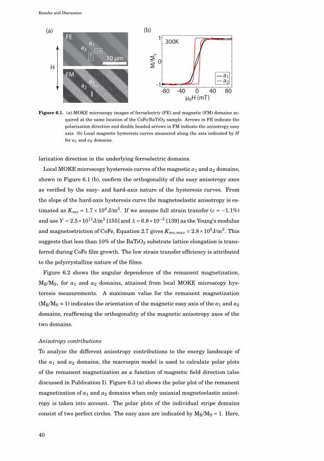
Results and Discussion
M/M
s
0
1
-10 40-40 80-80
μ0H (mT)
300K
a1
a1 a2
a1 a2 a2
FE
FM
10 μmH
(a) (b)
Figure 6.1. (a) MOKE microscopy images of ferroelectric (FE) and magnetic (FM) domains ac-quired at the same location of the CoFe/BaTiO3 sample. Arrows in FE indicate thepolarization direction and double headed arrows in FM indicate the anisotropy easyaxis. (b) Local magnetic hysteresis curves measured along the axis indicated by Hfor a1 and a2 domains.
larization direction in the underlying ferroelectric domains.
Local MOKE microscopy hysteresis curves of the magnetic a1 and a2 domains,
shown in Figure 6.1 (b), confirm the orthogonality of the easy anisotropy axes
as verified by the easy- and hard-axis nature of the hysteresis curves. From
the slope of the hard-axis hysteresis curve the magnetoelastic anisotropy is es-
timated as Kme = 1.7×10⁴ J/m3. If we assume full strain transfer (ε = −1.1%)
and use Y = 2.5×10¹¹J/m3 [155] and λ= 6.8×10⁻⁵ [139] as the Young’s modulus
and magnetostriction of CoFe, Equation 2.7 gives Kme,max = 2.8×10⁵J/m3. This
suggests that less than 10% of the BaTiO3 substrate lattice elongation is trans-
ferred during CoFe film growth. The low strain transfer efficiency is attributed
to the polycrystalline nature of the films.
Figure 6.2 shows the angular dependence of the remanent magnetization,
MR/MS, for a1 and a2 domains, attained from local MOKE microscopy hys-
teresis measurements. A maximum value for the remanent magnetization
(MR/MS ≈ 1) indicates the orientation of the magnetic easy axis of the a1 and a2
domains, reaffirming the orthogonality of the magnetic anisotropy axes of the
two domains.
Anisotropy contributions
To analyze the different anisotropy contributions to the energy landscape of
the a1 and a2 domains, the macrospin model is used to calculate polar plots
of the remanent magnetization as a function of magnetic field direction (also
discussed in Publication I). Figure 6.3 (a) shows the polar plot of the remanent
magnetization of a1 and a2 domains when only uniaxial magnetoelastic anisot-
ropy is taken into account. The polar plots of the individual stripe domains
consist of two perfect circles. The easy axes are indicated by MR/MS = 1. Here,
40
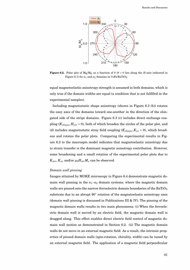
Results and Discussion
00.0
1.00
30
60
9
120
150180
210
240
270
300
330
1.0
MR/M
S
a1a2
Figure 6.2. Polar plot of MR/MS as a function of θ (θ = 0 lies along the H-axis indicated inFigure 6.1) for a1 and a2 domains in CoFe/BaTiO3.
equal magnetoelastic anisotropy strength is assumed in both domains, which is
only true if the domain widths are equal (a condition that is not fulfilled in the
experimental samples).
Including magnetostatic shape anisotropy (shown in Figure 6.3 (b)) rotates
the easy axes of the domains toward one-another in the direction of the elon-
gated side of the stripe domains. Figure 6.3 (c) includes direct exchange cou-
pling (Kshape,Hstr = 0), both of which broaden the circles of the polar plot, and
(d) includes magnetostatic stray field coupling (Kshape,Kex = 0), which broad-
ens and rotates the polar plots. Comparing the experimental results in Fig-
ure 6.2 to the macrospin model indicates that magnetoelastic anisotropy due
to strain transfer is the dominant magnetic anisotropy contribution. However,
some broadening and a small rotation of the experimental polar plots due to
Kms, Kex and/or μ0HstrMs can be observed.
Domain wall pinning
Images attained by MOKE microscopy in Figure 6.4 demonstrate magnetic do-
main wall pinning in the a1–a2 domain systems, where the magnetic domain
walls are pinned onto the narrow ferroelectric domain boundaries of the BaTiO3
substrate due to an abrupt 90◦ rotation of the magnetoelastic anisotropy axes
(domain wall pinning is discussed in Publications III & IV). The pinning of the
magnetic domain walls results in two main phenomena: (i) When the ferroele-
ctric domain wall is moved by an electric field, the magnetic domain wall is
dragged along. This effect enables direct electric field control of magnetic do-
main wall motion as demonstrated in Section 6.2. (ii) The magnetic domain
walls do not move in an external magnetic field. As a result, the intrinsic prop-
erties of pinned domain walls (spin-rotation, chirality, width) can be tuned by
an external magnetic field. The application of a magnetic field perpendicular
41

Results and Discussion
0
0.0
0.5
1.00
30
60
90
120
150180
210
240
270
300
330
0.5
1.0
�oHstrM
0.81.6
0.81.6
�oHstrMa1 a2
Kme = 1.0, Kms = 0, Kex = 0
0.0
0.5
1.00
30
60
90
120
150180
210
240
270
300
330
0.5
1.0
a1 a2Kms Kms
0.40.8
0.40.8
Kme = 1.0, Kex�������oHstrM = 0
0.0
0.5
1.00
30
60
9
120
150180
210
240
270
300
330
0.5
1.0
a1 a2Kme Kme
1.0 1.0
Kms = 0, Kex�������oHstrM = 0
Kme = 1.0, Kms�������oHstrM = 0
0.0
0.5
1.0
0.5
1.0
0.4
0.80.40.8
a1 a2Kex Kex
030
60
90
120
150180
210
240
270
300
330
(a) (b)
(c) (d)
MR/
MS
MR/
MS
MR/
MS
MR/
MS
Figure 6.3. Simulated polar plots of MR /MS as a function of θ for a1 and a2 domains usingEquations 5.1 and 5.2. The contribution of (a) Kme, (b) Kme and Kms, (c) Kme andKex and (d) Kme and μ0Hstr Ms are compared.
42

Results and Discussion
56 mT
10 mT
FM
FE 0 mT
-10 mT
-74 mT
H H
Figure 6.4. Ferroelectric (FE) domain image and magnetic (FM) domain images as a function ofmagnetic field strength for CoFe/BaTiO3. The magnetic domain walls do not movedue to strong pinning on to the ferroelectric domain boundaries.
to the domain walls results in the formation of narrow uncharged walls, while
broad charged domain walls form when a field is applied parallel to the walls.
Figure 6.5 shows the remanent magnetic spin structure after applying mag-
netic fields in these two field directions. The width of the domain wall is about
an order magnitude larger for the charged domain walls due to an additional
magnetostatic contribution to the domain wall energy (shown in Figure 6.5 (c)).
Besides the width, the spin rotation in domain walls can also be tuned by vari-
ation of the magnetic field strength (shown in Figure 6.5 (d)).
6.1.2 Fe/BaTiO3
The competition between magnetocrystalline and magnetoelastic anisotropies
with laterally modulating symmetry is studied in epitaxial Fe films grown onto
BaTiO3 substrates containing a–c domains, schematically illustrated in Fig-
ure 6.6 (a). Transmission electron microscopy measurements confirm growth
of epitaxial Fe films on top of BaTiO3 with Fe[110] ‖ BTO[100] [Publication IV].
Through strain transfer at the substrate–film interface the crystalline Fe film is
laterally compressed by the ferroelectric domains. The ferroelectric a–domains
compress the Fe lattice by 1.6% and 0.6% in the [110]Fe and [110]Fe directions
respectively, creating a local uniaxial magnetoelastic easy axis parallel to the
domain wall. The ferroelectric c–domains compress the Fe lattice biaxially
along [110]Fe and [110]Fe by 1.6%. The 1.6% compression is not sufficient to
overcome the magnetocrystalline anisotropy of Fe (see Section 2.3.1). Hence,
the magnetization easy axes in the c–domains lie along ⟨100⟩Fe which are fa-
43
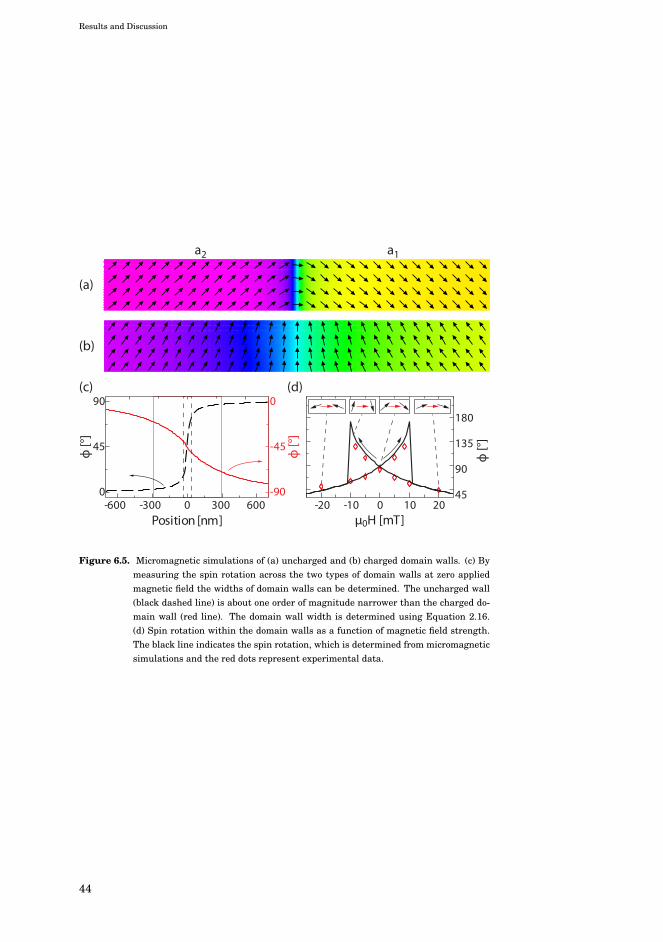
Results and Discussion
(a)
(b)
(c) (d)
a2 a1
-600 -300 0 300 6000
45
90
-90
-45
0
ф [°
]
ф [°
]
Position [nm] μ0H [mT]
ф [°
]
-20 -10 0 10 2045
90
135
180
Figure 6.5. Micromagnetic simulations of (a) uncharged and (b) charged domain walls. (c) Bymeasuring the spin rotation across the two types of domain walls at zero appliedmagnetic field the widths of domain walls can be determined. The uncharged wall(black dashed line) is about one order of magnitude narrower than the charged do-main wall (red line). The domain wall width is determined using Equation 2.16.(d) Spin rotation within the domain walls as a function of magnetic field strength.The black line indicates the spin rotation, which is determined from micromagneticsimulations and the red dots represent experimental data.
44
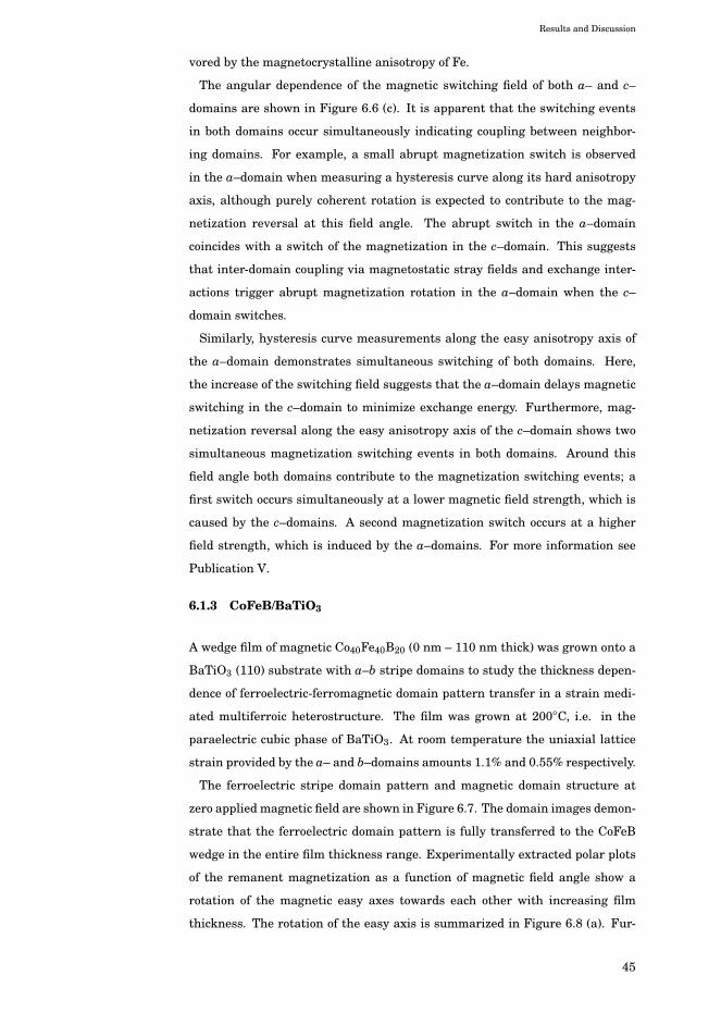
Results and Discussion
vored by the magnetocrystalline anisotropy of Fe.
The angular dependence of the magnetic switching field of both a– and c–
domains are shown in Figure 6.6 (c). It is apparent that the switching events
in both domains occur simultaneously indicating coupling between neighbor-
ing domains. For example, a small abrupt magnetization switch is observed
in the a–domain when measuring a hysteresis curve along its hard anisotropy
axis, although purely coherent rotation is expected to contribute to the mag-
netization reversal at this field angle. The abrupt switch in the a–domain
coincides with a switch of the magnetization in the c–domain. This suggests
that inter-domain coupling via magnetostatic stray fields and exchange inter-
actions trigger abrupt magnetization rotation in the a–domain when the c–
domain switches.
Similarly, hysteresis curve measurements along the easy anisotropy axis of
the a–domain demonstrates simultaneous switching of both domains. Here,
the increase of the switching field suggests that the a–domain delays magnetic
switching in the c–domain to minimize exchange energy. Furthermore, mag-
netization reversal along the easy anisotropy axis of the c–domain shows two
simultaneous magnetization switching events in both domains. Around this
field angle both domains contribute to the magnetization switching events; a
first switch occurs simultaneously at a lower magnetic field strength, which is
caused by the c–domains. A second magnetization switch occurs at a higher
field strength, which is induced by the a–domains. For more information see
Publication V.
6.1.3 CoFeB/BaTiO3
A wedge film of magnetic Co40Fe40B20 (0 nm – 110 nm thick) was grown onto a
BaTiO3 (110) substrate with a–b stripe domains to study the thickness depen-
dence of ferroelectric-ferromagnetic domain pattern transfer in a strain medi-
ated multiferroic heterostructure. The film was grown at 200◦C, i.e. in the
paraelectric cubic phase of BaTiO3. At room temperature the uniaxial lattice
strain provided by the a– and b–domains amounts 1.1% and 0.55% respectively.
The ferroelectric stripe domain pattern and magnetic domain structure at
zero applied magnetic field are shown in Figure 6.7. The domain images demon-
strate that the ferroelectric domain pattern is fully transferred to the CoFeB
wedge in the entire film thickness range. Experimentally extracted polar plots
of the remanent magnetization as a function of magnetic field angle show a
rotation of the magnetic easy axes towards each other with increasing film
thickness. The rotation of the easy axis is summarized in Figure 6.8 (a). Fur-
45
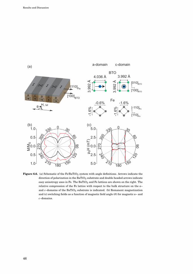
Results and Discussion
30
0.0
2.5
5.0 0 30
6090
120
150180
210
240
270
300
330
2.5
5.0
� 0H
(mT)
0.0
0.5
1.0 0
6090
120
150180
210
240
270
300
330
0.5
1.0
M/M
S
(b) (c)
a a ac c
H, ��
(a)
[110]Fe
[100]BTO
Fe
-1.6
%
-1.6%-0.6%
-1.6
%[110]Fe
[-110]Fe
a-domain c-domain
BTO
3.99
2 Å
4.036 Å 3.992 Å
3.99
2 Å
[100]BTO
[010]BTO
Figure 6.6. (a) Schematic of the Fe/BaTiO3 system with angle definitions. Arrows indicate thedirection of polarization in the BaTiO3 substrate and double headed arrows indicateeasy anisotropy axes in Fe. The BaTiO3 and Fe lattices are shown on the right. Therelative compression of the Fe lattice with respect to the bulk structure on the a–and c–domains of the BaTiO3 substrate is indicated. (b) Remanent magnetizationand (c) switching fields as a function of magnetic field angle (θ) for magnetic a– andc–domains.
46
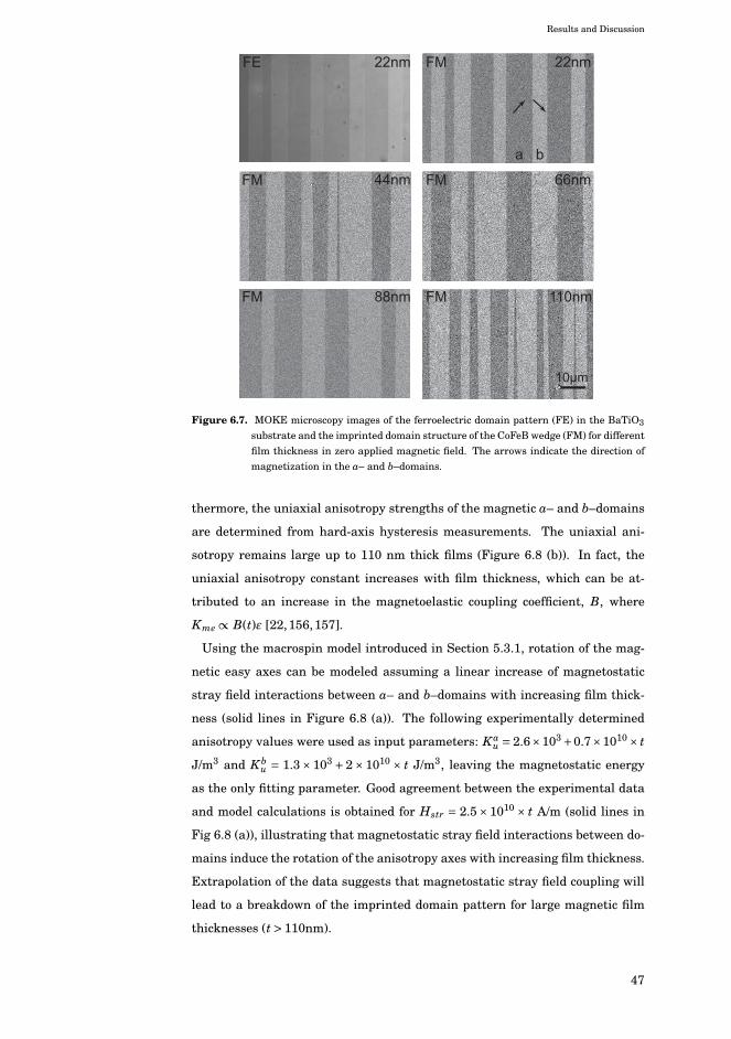
Results and Discussion
FE FM
FMFM
FMFM
22nm22nm
66nm44nm
88nm 110nm
10�m
a b
Figure 6.7. MOKE microscopy images of the ferroelectric domain pattern (FE) in the BaTiO3substrate and the imprinted domain structure of the CoFeB wedge (FM) for differentfilm thickness in zero applied magnetic field. The arrows indicate the direction ofmagnetization in the a– and b–domains.
thermore, the uniaxial anisotropy strengths of the magnetic a– and b–domains
are determined from hard-axis hysteresis measurements. The uniaxial ani-
sotropy remains large up to 110 nm thick films (Figure 6.8 (b)). In fact, the
uniaxial anisotropy constant increases with film thickness, which can be at-
tributed to an increase in the magnetoelastic coupling coefficient, B, where
Kme ∝ B(t)ε [22,156,157].
Using the macrospin model introduced in Section 5.3.1, rotation of the mag-
netic easy axes can be modeled assuming a linear increase of magnetostatic
stray field interactions between a– and b–domains with increasing film thick-
ness (solid lines in Figure 6.8 (a)). The following experimentally determined
anisotropy values were used as input parameters: Kau = 2.6×10³+0.7×10¹⁰× t
J/m3 and Kbu = 1.3×10³ +2×10¹⁰ × t J/m3, leaving the magnetostatic energy
as the only fitting parameter. Good agreement between the experimental data
and model calculations is obtained for Hstr = 2.5×10¹⁰ × t A/m (solid lines in
Fig 6.8 (a)), illustrating that magnetostatic stray field interactions between do-
mains induce the rotation of the anisotropy axes with increasing film thickness.
Extrapolation of the data suggests that magnetostatic stray field coupling will
lead to a breakdown of the imprinted domain pattern for large magnetic film
thicknesses (t > 110nm).
47

Results and Discussion
0 20 40 60 80 10040
60
80
100
120
Eas
y-ax
is a
ngle
(º)
t (nm)(b)
(a)
Ku (
kJ /
m3 )
t (nm)0 20 40 60 80 100
3
4
5
6
2
a-domain b-domain
a-domain b-domain
Figure 6.8. (a) Angle of the easy magnetization axis and (b) uniaxial magnetic anisotropy asa function of CoFeB film thickness. Solid lines in (a) are fits using the macrospinmodel (Equations 5.1 & 5.2). In this model, a linear increase of the magnetostaticstray field anisotropy with film thickness is assumed. The experimentally deter-mined values for Ku are used.
48
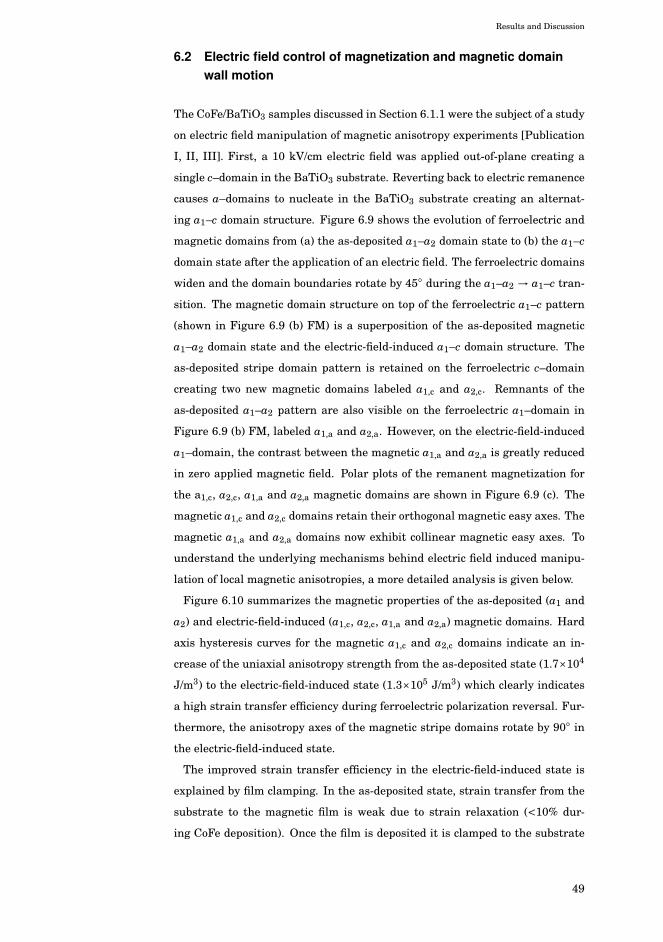
Results and Discussion
6.2 Electric field control of magnetization and magnetic domainwall motion
The CoFe/BaTiO3 samples discussed in Section 6.1.1 were the subject of a study
on electric field manipulation of magnetic anisotropy experiments [Publication
I, II, III]. First, a 10 kV/cm electric field was applied out-of-plane creating a
single c–domain in the BaTiO3 substrate. Reverting back to electric remanence
causes a–domains to nucleate in the BaTiO3 substrate creating an alternat-
ing a1–c domain structure. Figure 6.9 shows the evolution of ferroelectric and
magnetic domains from (a) the as-deposited a1–a2 domain state to (b) the a1–c
domain state after the application of an electric field. The ferroelectric domains
widen and the domain boundaries rotate by 45◦ during the a1–a2 → a1–c tran-
sition. The magnetic domain structure on top of the ferroelectric a1–c pattern
(shown in Figure 6.9 (b) FM) is a superposition of the as-deposited magnetic
a1–a2 domain state and the electric-field-induced a1–c domain structure. The
as-deposited stripe domain pattern is retained on the ferroelectric c–domain
creating two new magnetic domains labeled a1,c and a2,c. Remnants of the
as-deposited a1–a2 pattern are also visible on the ferroelectric a1–domain in
Figure 6.9 (b) FM, labeled a1,a and a2,a. However, on the electric-field-induced
a1–domain, the contrast between the magnetic a1,a and a2,a is greatly reduced
in zero applied magnetic field. Polar plots of the remanent magnetization for
the a1,c, a2,c, a1,a and a2,a magnetic domains are shown in Figure 6.9 (c). The
magnetic a1,c and a2,c domains retain their orthogonal magnetic easy axes. The
magnetic a1,a and a2,a domains now exhibit collinear magnetic easy axes. To
understand the underlying mechanisms behind electric field induced manipu-
lation of local magnetic anisotropies, a more detailed analysis is given below.
Figure 6.10 summarizes the magnetic properties of the as-deposited (a1 and
a2) and electric-field-induced (a1,c, a2,c, a1,a and a2,a) magnetic domains. Hard
axis hysteresis curves for the magnetic a1,c and a2,c domains indicate an in-
crease of the uniaxial anisotropy strength from the as-deposited state (1.7×10⁴
J/m3) to the electric-field-induced state (1.3×10⁵ J/m3) which clearly indicates
a high strain transfer efficiency during ferroelectric polarization reversal. Fur-
thermore, the anisotropy axes of the magnetic stripe domains rotate by 90◦ in
the electric-field-induced state.
The improved strain transfer efficiency in the electric-field-induced state is
explained by film clamping. In the as-deposited state, strain transfer from the
substrate to the magnetic film is weak due to strain relaxation (<10% dur-
ing CoFe deposition). Once the film is deposited it is clamped to the substrate
49
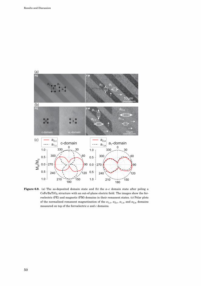
Results and Discussion
(a)
(b)FE
a1-domainc-domain
a2
a2,c
a1,c
a1,a
a2,a
a1
FM
FE FM
10�
10�
a2 a1
0.0
0.5
1.00
30
60
90
120
150180
210
240
270
300
330
0.5
1.0
0.0
0.5
1.0
0.5
1.0
030
60
90
120
150180
210
240
270
300
330
MR/M
S
(c) a2,ca1,c
a2,aa1,a
c-domain a1-domain
Figure 6.9. (a) The as-deposited domain state and (b) the a–c domain state after poling aCoFe/BaTiO3 structure with an out-of-plane electric field. The images show the fer-roelectric (FE) and magnetic (FM) domains in their remanent states. (c) Polar plotsof the normalized remanent magnetization of the a1,c, a2,c, a1,a and a2,a domainsmeasured on top of the ferroelectric a and c domains.
50
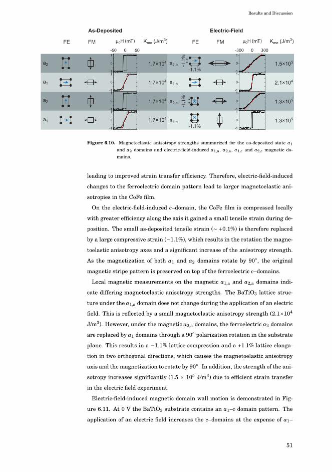
Results and Discussion
Electric-Field
FE FMFMFE
1.5×10⁵
2.1×10⁴
1.3×10⁵
Kme (J/m3)
1.7×10⁴
1.7×10⁴
1.7×10⁴
1.7×10⁴
As-Deposited
a1
a2
a1
a2
a1,a
a2,c
a1,c
a2,a
1.3×10⁵
-60 0 60
0
-1
1
0
-1
1
0
-1
1
0
-1
1
-300 0 300
0
-1
1
0
-1
1
0
-1
1
0
-1
1
μ0H (mT) Kme (J/m3)μ0H (mT)
-1.1
%-1
.1%
-1.1%
-1.1%
Figure 6.10. Magnetoelastic anisotropy strengths summarized for the as-deposited state a1and a2 domains and electric-field-induced a1,a, a2,a, a1,c and a2,c magnetic do-mains.
leading to improved strain transfer efficiency. Therefore, electric-field-induced
changes to the ferroelectric domain pattern lead to larger magnetoelastic ani-
sotropies in the CoFe film.
On the electric-field-induced c–domain, the CoFe film is compressed locally
with greater efficiency along the axis it gained a small tensile strain during de-
position. The small as-deposited tensile strain (∼ +0.1%) is therefore replaced
by a large compressive strain (−1.1%), which results in the rotation the magne-
toelastic anisotropy axes and a significant increase of the anisotropy strength.
As the magnetization of both a1 and a2 domains rotate by 90◦, the original
magnetic stripe pattern is preserved on top of the ferroelectric c–domains.
Local magnetic measurements on the magnetic a1,a and a2,a domains indi-
cate differing magnetoelastic anisotropy strengths. The BaTiO3 lattice struc-
ture under the a1,a domain does not change during the application of an electric
field. This is reflected by a small magnetoelastic anisotropy strength (2.1×10⁴
J/m3). However, under the magnetic a2,a domains, the ferroelectric a2 domains
are replaced by a1 domains through a 90◦ polarization rotation in the substrate
plane. This results in a −1.1% lattice compression and a +1.1% lattice elonga-
tion in two orthogonal directions, which causes the magnetoelastic anisotropy
axis and the magnetization to rotate by 90◦. In addition, the strength of the ani-
sotropy increases significantly (1.5 × 10⁵ J/m3) due to efficient strain transfer
in the electric field experiment.
Electric-field-induced magnetic domain wall motion is demonstrated in Fig-
ure 6.11. At 0 V the BaTiO3 substrate contains an a1–c domain pattern. The
application of an electric field increases the c–domains at the expense of a1–
51

Results and Discussion
0V
40V
FE
FM
80V
100V
120V
50�m
Figure 6.11. Magnetic domain wall motion induced by an electric field. Ferroelectric (FE) andmagnetic (FM) domain states at 0V−120V indicate the writing of magnetic stripepatterns by lateral magnetic domain wall motion. All images are acquired withHex = 0.
domains by lateral ferroelectric domain wall motion. The magnetic domain
walls, which are pinned onto the ferroelectric domain boundaries by abrupt
changes in the magnetoelastic anisotropy, are dragged along. Furthermore, the
magnetic a1,c and a2,c stripe domains are rewritten because the motion of the
ferroelectric boundary changes the local magnetic anisotropy of the CoFe film.
This is a reversible process, whereby the magnetic a1,c and a2,c domain pattern
is erased by the formation of ferroelectric a–domains once the electric field is
removed. The data in Figure 6.11 demonstrates for the first time that mag-
netic domain wall motion can be fully controlled by an electric field without the
need for an external magnetic field. Traditionally, magnetization rotation and
magnetic domain wall motion are induced by an external magnetic field or an
electric current through a magnetic nanowire. The ability to erase and rewrite
domain patterns and to move magnetic domain walls by purely electrical means
opens up routes towards electrically controllable low power magnetic devices.
6.3 Temperature control of magnetic anisotropy
Structural phase changes in BaTiO3 can also be used to locally strain a mag-
netic film (as described in Section 6.1.1). Temperature induced magnetic do-
main control is demonstrated in samples consisting of CoFe films grown onto
52
Results and Discussion
BaTiO3 substrates [Publication VI].
In the experiments, the magnetic domains are imaged using MOKE micro-
scopy while temperature cycling the BaTiO3 substrate through its rhombohe-
dral (R), orthorhombic (O), tetragonal (T) and cubic (C) phases. Figure 6.12
shows the magnetic domain structure in zero applied magnetic field and hys-
teresis curves before and after the temperature induced structural phase tran-
sitions. To begin, the CoFe/BaTiO3 sample with an a1–a2 domain pattern was
cooled from room temperature through the T → O phase transition. Magnetic
contrast images in Figure 6.12 show that the contrast in the magnetic domains
is reversed indicating a 90◦ rotation of the magnetization direction during cool-
ing (300K → 270K). Figure 3.2 shows that cooling BaTiO3 from room temper-
ature to the orhtorhombic phase compresses the CoFe lattice along the c–axis.
The direction of lattice compression is parallel to the small tensile strain that
was obtained during CoFe film growth on tetragonal BaTiO3. Furthermore, the
CoFe film is slightly elongated along the b–axis. Due to film clamping, strain
transfer during cooling is about one order of magnitude more efficient than
during growth. Hence, the strain in the magnetic domains evolves from a weak
tensile strain to a strong compressive strain, which causes the magnetoelastic
anisotropy axes to rotate by 90◦. Additionally to a rotation of the anisotropy
axes, the saturation field of the hard axis hysteresis curve increases from 20
mT in the tetragonal phase to 170 mT in the orthorhombic phase, increasing
the uniaxial anisotropy strength from 1.7×10⁴ J/m3 to 1.4×10⁵ J/m3, reaffirm-
ing the increase in strain transfer efficiency.
Cooling the sample through the O → R phase transition does not change the
magnetic contrast of the domain pattern (Figure 6.12 250K → 170K). As a re-
sult of this phase transition the rhombohedral phase locally compresses the
CoFe film along the c–axis, whilst decreasing the local tensile strain along the
b–axis. Hence, only a small increase in magnetic anisotropy strength is ob-
served (saturation field 170mT→ 200mT).
Upon heating the sample from the tetragonal phase to the cubic phase of the
BaTiO3 substrate, the magnetic contrast is again reversed (Figure 6.12, 300
K → 420 K). Similarly to the T → O phase transition, the BaTiO3 lattice com-
presses the CoFe film locally along the c–axis in the cubic phase. Futhermore,
the cubic phase of BaTiO3 induces a tensile strain along the b–axis in the CoFe
film. Due to film clamping this results in a 90◦ rotation of the magnetic anisot-
ropy axes. Unlike the abrupt T → O and O → R phase transitions, the T → C
transition is gradual taking place over a temperature range of 320 K to 420 K.
From 360 K to 390 K the growth-induced uniaxial tensile strain in the CoFe
53
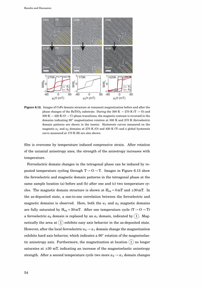
Results and Discussion
M/M
s
0
1
-1
270KM
/Ms
0
1
-1
M/M
s
0
1
-1
170K 420K
0 80-80�0H (mT)
0 80-80�0H (mT)
0 80-80�0H (mT)
a1a2
a1a2
FE
FE
20�m 20�m
Figure 6.12. Images of CoFe domain structure at remanent magnetization before and after thephase changes of the BaTiO3 substrate. During the 300 K → 270 K (T → O) and300 K → 420 K (O → C) phase transitions, the magnetic contrast is reversed in thedomains indicating 90◦ magnetization rotation at 300 K and 270 K (ferroelectricdomain patterns are shown in the insets). Hysteresis curves measured on themagnetic a1 and a2 domains at 270 K (O) and 420 K (T) and a global hysteresiscurve measured at 170 K (R) are also shown.
film is overcome by temperature induced compressive strain. After rotation
of the uniaxial anisotropy axes, the strength of the anisotropy increases with
temperature.
Ferroelectric domain changes in the tetragonal phase can be induced by re-
peated temperature cycling through T→O→T. Images in Figure 6.13 show
the ferroelectric and magnetic domain patterns in the tetragonal phase at the
same sample location (a) before and (b) after one and (c) two temperature cy-
cles. The magnetic domain structure is shown at Hex = 0mT and ±30mT. In
the as-deposited state, a one-to-one correlation between the ferroelectric and
magnetic domains is observed. Here, both the a1 and a2 magnetic domains
are fully saturated by Hex = 30mT. After one temperature cycle (T→O→T)
a ferroelectric a2 domain is replaced by an a1 domain, indicated by 1 . Mag-
netically the area at 1 exhibits easy axis behavior in the as-deposited state.
However, after the local ferroelectric a2 → a1 domain change the magnetization
exhibits hard axis behavior, which indicates a 90◦ rotation of the magnetoelas-
tic anisotropy axis. Furthermore, the magnetization at location 1 no longer
saturates at ±30 mT, indicating an increase of the magnetoelastic anisotropy
strength. After a second temperature cycle two more a2 → a1 domain changes
54

Results and Discussion
occur (indicated by 2 ). Again, rotations of the magnetoelastic anisotropy axes
are observed at these locations along with an increase in magnetoelastic ani-
sotropy strength. The saturation fields for the new stripe domains is 600 mT,
which gives Kme = 5.1×10⁵ J/m3, a value that is almost 2Kme,max (see Section
6.1.1). This is expected for full strain transfer as the CoFe film is compressed
by -1.1% and elongated by +1.1% in two orthogonal directions. Finally, an a2
domain grew in size leading to a rotation of the magnetoelastic anisotropy axis
from hard axis to easy axis at 3 . Again, a 90◦ rotation of magnetoelastic
anisotropy axis is observed with rotation of the underlying ferroelectric polar-
ization.
The underlying mechanism for the rotation and strengthening of the uniaxial
anisotropy axis has been discussed in detail in Section 6.2. During deposition,
strain transfer from the BaTiO3 substrate to the CoFe film is weak. If a ferro-
electric domain change (a1 → a2 or a2 → a1) is induced after deposition, much
larger strains are transferred to the magnetic film. The ferroelectric domain
change induces a −1.1% compression and a 1.1% elongation in two orthogonal
directions. This results in a 90◦ rotation of the magnetoelastic anisotropy axes
and an increase of the magnetoelastic anisotropy strength.
Although local changes to the ferroelectric domain pattern result in changes
of the magnetoelastic anisotropy strength, the magnetic domain pattern at zero
applied magnetic field always matches the underlying ferroelectric domains (if
the ferroelectric polarization is in-plane). This provides a direct link between
the direction of the polarization and magnetoelastic anisotropy, which can be
utilized in future electric field controlled magnetic structures.
55
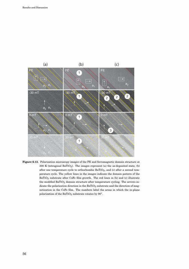
Results and Discussion
FE
-30 mT
0 mT 0 mT 0 mT
30 mT 30 mT 30 mT
-30 mT -30 mT
FE1
1
1
1
2
3
2 2
(a) (b) (c)
a1 a1a2 a1a2
a1a2
a1a2
a1a2
a2
FE
Figure 6.13. Polarization microscopy images of the FE and ferromagnetic domain structure at300 K (tetragonal BaTiO3). The images represent (a) the as-deposited state, (b)after one temperature cycle to orthorhombic BaTiO3, and (c) after a second tem-perature cycle. The yellow lines in the images indicate the domain pattern of theBaTiO3 substrate after CoFe film growth. The red lines in (b) and (c) illustratethe modified BaTiO3 domain structure after temperature cycling. The arrows in-dicate the polarization direction in the BaTiO3 substrate and the direction of mag-netization in the CoFe film. The numbers label the areas in which the in-planepolarization of the BaTiO3 substrate rotates by 90◦.
56
7. Conclusions
Ferroelectric-ferromagnetic domain coupling in multiferroic heterostructures
has been studied using optical polarization microscopy techniques. The results
presented in this thesis demonstrate three major developments in the control
of magnetic domains in strain-mediated multiferroic heterostructures: Firstly,
it was shown that non-180◦ ferroelectric domain patterns in BaTiO3 substrates
are fully transferable to several different types of magnetic films through in-
terfacial strain transfer and inverse magnetostiction. Secondly, electrical con-
trol of magnetization rotation and magnetic domain wall motion were achieved
due to strong coupling between the magnetic and ferroelectric domains. Fi-
nally, during temperature-induced structural phase transitions in the BaTiO3
substrate the magnetization of the magnetic film closely follows the in-plane
rotation of the ferroelectric polarization.
Ferroelectric pattern transfer was demonstrated in multiferroic heterostruc-
tures using three different magnetic films: Magnetic polycrystalline CoFe, epi-
taxial Fe and amorphous CoFeB films all exhibited domain imprinting from
ferroelectric BaTiO3 substrates. Strain transfer from the regular, non-180◦ fer-
roelectric domain structures creates a well-defined magnetic domain pattern in
the magnetic films. Abrupt in-plane rotations of the magnetoelastic anisotropy
axes at ferroelectric domain boundaries forms pinning sites for the magnetic
domain walls, immobilizing them during magnetization reversal. This well-
defined, controllable magnetic domain structure provides the ability to tune
magnetic domain properties, such as spin rotation and domain wall width, us-
ing an external magnetic field. Such magnetic domain patterns can be used
as a basis to study a variety of different magnetic phenomenon including mag-
netic domain wall resistance and magnon propagation through magnetic do-
main walls.
Strong coupling of the magnetic domains to their ferroelectric counterparts
was used to demonstrate electrical control of magnetization in CoFe/BaTiO3.
57
Conclusions
The motion of ferroelectric domain boundaries in an applied electric field caused
the pinned magnetic domain walls to be dragged along resulting in electric-
field-induced propagation of magnetic domain walls. For the first time, electric
field controlled magnetic domain wall motion and local magnetization rotations
have been demonstrated, providing a platform to study domain coupling and
magnetic domain wall motion in more intricate multiferroic heterostructures.
Understanding the microscopic phenomenon in multiferroic heterostructures
can pave the way towards low energy magnetic actuators and spintronic de-
vices. The in-depth analysis of magnetization reversal processes – including
domain coupling and the effects of inter-domain interactions – and electric-
field-induced magnetic domain wall motion have provided new insights into
the physics of electric field controlled magnetism. This provides a foundation
for studies on electric field control of local magnetization in multiferroics con-
sisting purely of thin film structures, miniaturized multiferroic systems and
electric field control of domain wall logic devices.
58
Bibliography
[1] N. A. SPALDIN and M. FIEBIG, Science 309, 391 (2005).
[2] J. STÖHR and H. C. SIEGMANN, Magnetism: From Fundamentals to NanoscaleDynamics, Springer, 2006.
[3] S. BLUNDELL, Magnetism in Condensed Matter, Oxford University Press, 2010.
[4] C. L. DENNIS, R. P. BORGES, L. D. BUDA, U. EBELS, J. F. GREGG, M. HEHN,E. JOUGUELET, K. OUNADJELA, I. PETEJ, I. L. PREJBEANU, and M. J. THORN-TON, Journal of Physics: Condensed Matter 14, R1175 (2002).
[5] C. A. F. VAZ, J. A. C. BLAND, and G. LAUHOFF, Reports on Progress in Physics71, 056501 (2008).
[6] R. O’HANDLEY, Modern Magnetic Materials: Principles and Applications, JohnWiley & Sons Inc., 2000.
[7] J. A. OSBORN, Physical Review 67, 351 (1945).
[8] J. DUBOWIK, Physical Review B 54, 1088 (1996).
[9] M. GRIMSDITCH, Y. JACCARD, and I. K. SCHULLER, Physical Review B 58,11539 (1998).
[10] M. DARBY and E. ISAAC, IEEE Transactions on Magnetics 10, 259 (1974).
[11] R. C. HALL, Journal of Applied Physics 30, 816 (1959).
[12] C. KITTEL, Physical Review Letters 3, 169 (1959).
[13] D.-S. WANG, R. WU, and A. J. FREEMAN, Physical Review B 47, 14932 (1993).
[14] E. CALLEN, Journal of Applied Physics 39, 519 (1968).
[15] E. CALLEN and H. B. CALLEN, Physical Review 139, A455 (1965).
[16] R. C. O’HANDLEY, Physical Review B 18, 930 (1978).
[17] C. ROBINSON, M. SAMANT, and E. MARINERO, Applied Physics A 49, 619(1989).
[18] X. YAN, M. HIRSCHER, T. EGAMI, and E. E. MARINERO, Physical Review B 43,9300 (1991).
[19] V. G. HARRIS, K. D. AYLESWORTH, B. N. DAS, W. T. ELAM, and N. C. KOON,Physical Review Letters 69, 1939 (1992).
59
Bibliography
[20] J. FURTHMULLER, M. FAHNLE, and G. HERZER, Journal of Physics F: MetalPhysics 16, L255 (1986).
[21] M. FÄHNLE and T. EGAMI, Journal of Applied Physics 53, 2319 (1982).
[22] D. SANDER, Reports on Progress in Physics 62, 809 (1999).
[23] J. P. JAKUBOVICS, Philosophical Magazine Part B 38, 401 (1978).
[24] B. D. CULLITY and C. D. GRAHAM, Introduntion to Magnetic Materials, SecondEdition, John Wiley & Sons Inc., 2009.
[25] A. HUBERT and R. SCHÄFER, Magnetic Domains: The Analytics of MagneticMicrostructures, Springer, New York, 1998.
[26] C. KITTEL, Reviews of Modern Physics 21, 541 (1949).
[27] S. S. P. PARKIN, M. HAYASHI, and L. THOMAS, Science 320, 190 (2008).
[28] L. K. BOGART, D. ATKINSON, K. O’SHEA, D. MCGROUTHER, and S. MCVITIE,Physical Review B 79, 054414 (2009).
[29] D. I. PAUL, Journal of Applied Physics 53, 1649 (1982).
[30] V. H. SCHMIDT, Ferroelectrics 72, 157 (1987).
[31] R. E. COHEN, Nature 358, 136 (1992).
[32] R. COHEN, Journal of Physics and Chemistry of Solids 61, 139 (2000).
[33] C. KITTEL, Introduction to Solid State Physics, John Wiley & Sons Inc., 2005.
[34] A. VON HIPPEL, Reviews of Modern Physics 22, 221 (1950).
[35] H. D. MEGAW, Proceedings of the Royal Society of London. Series A. Mathemat-ical and Physical Sciences 189, 261 (1947).
[36] G. H. KWEI, A. C. LAWSON, S. J. L. BILLINGE, and S. W. CHEONG, The Journalof Physical Chemistry 97, 2368 (1993).
[37] G. SHIRANE, H. DANNER, and R. PEPINSKY, Physical Review 105, 856 (1957).
[38] S. K. STREIFFER, J. A. EASTMAN, D. D. FONG, C. THOMPSON, A. MUNKHOLM,M. V. RAMANA MURTY, O. AUCIELLO, G. R. BAI, and G. B. STEPHENSON,Physical Review Letters 89, 067601 (2002).
[39] N. A. PERTSEV and A. G. ZEMBILGOTOV, Journal of Applied Physics 78, 6170(1995).
[40] S. PÖYKKÖ and D. J. CHADI, Applied Physics Letters 75, 2830 (1999).
[41] B. MEYER and D. VANDERBILT, Physical Review B 65, 104111 (2002).
[42] P. MARTON, I. RYCHETSKY, and J. HLINKA, Physical Review B 81, 144125(2010).
[43] X. ZHANG, T. HASHIMOTO, and D. C. JOY, Applied Physics Letters 60, 784(1992).
[44] J. HLINKA and P. MÁRTON, Physical Review B 74, 104104 (2006).
60
Bibliography
[45] Q. Z. W. A. GODDARD and III, Applied Physics Letters 89, 182903 (2006).
[46] M. FIEBIG, Journal of Physics D: Applied Physics 38, R123 (2005).
[47] W. EERENSTEIN, N. D. MATHUR, and J. F. SCOTT, Nature 442, 759 (2006).
[48] R. RAMESH and N. A. SPALDIN, Nature Materials 6, 21 (2007).
[49] C.-W. NAN, M. I. BICHURIN, S. DONG, D. VIEHLAND, and G. SRINIVASAN,Journal of Applied Physics 103, 031101 (2008).
[50] M. BIBES and A. BARTHELEMY, Nature Materials 7, 425 (2008).
[51] J. MA, J. HU, Z. LI, and C.-W. NAN, Advanced Materials 23, 1062 (2011).
[52] C. A. F. VAZ, Journal of Physics: Condensed Matter 24, 333201 (2012).
[53] J. WANG, J. B. NEATON, H. ZHENG, V. NAGARAJAN, S. B. OGALE, B. LIU,D. VIEHLAND, V. VAITHYANATHAN, D. G. SCHLOM, U. V. WAGHMARE, N. A.SPALDIN, K. M. RABE, M. WUTTIG, and R. RAMESH, Science 299, 1719 (2003).
[54] J. DHO, X. QI, H. KIM, J. L. MACMANUS-DRISCOLL, and M. G. BLAMIRE,Advanced Materials 18, 1445 (2006).
[55] C. EDERER and N. A. SPALDIN, Physical Review B 71, 060401 (2005).
[56] J. B. NEATON, C. EDERER, U. V. WAGHMARE, N. A. SPALDIN, and K. M. RABE,Physical Review B 71, 014113 (2005).
[57] H. BÁ, M. BIBES, A. BARTHÉLÉMY, K. BOUZEHOUANE, E. JACQUET, A. KHO-DAN, J.-P. CONTOUR, S. FUSIL, F. WYCZISK, A. FORGET, D. LEBEUGLE,D. COLSON, and M. VIRET, Applied Physics Letters 87, 072508 (2005).
[58] T. ZHAO, A. SCHOLL, F. ZAVALICHE, K. LEE, M. BARRY, A. DORAN, M. P.CRUZ, Y. H. CHU, C. EDERER, N. A. SPALDIN, R. R. DAS, D. M. KIM, S. H.BAEK, C. B. EOM, and R. RAMESH, Nature Materials 5, 823 (2006).
[59] T. KIMURA, T. GOTO, H. SHINTANI, K. ISHIZAKA, T. ARIMA, and Y. TOKURA,Nature 426, 55 (2003).
[60] N. HUR, S. PARK, P. A. SHARMA, J. S. AHN, S. GUHA, and S.-W. CHEONG,Nature 429, 392 (2004).
[61] Y. TOKURA and S. SEKI, Advanced Materials 22, 1554 (2010).
[62] H. ZHENG, J. WANG, S. E. LOFLAND, Z. MA, L. MOHADDES-ARDABILI,T. ZHAO, L. SALAMANCA-RIBA, S. R. SHINDE, S. B. OGALE, F. BAI,D. VIEHLAND, Y. JIA, D. G. SCHLOM, M. WUTTIG, A. ROYTBURD, andR. RAMESH, Science 303, 661 (2004).
[63] J. LI, I. LEVIN, J. SLUTSKER, V. PROVENZANO, P. K. SCHENCK, R. RAMESH,J. OUYANG, and A. L. ROYTBURD, Applied Physics Letters 87, 072909 (2005).
[64] F. ZAVALICHE, H. ZHENG, L. MOHADDES-ARDABILI, S. Y. YANG, Q. ZHAN,P. SHAFER, E. REILLY, R. CHOPDEKAR, Y. JIA, P. WRIGHT, D. G. SCHLOM,Y. SUZUKI, and R. RAMESH, Nano Letters 5, 1793 (2005).
[65] I. LEVIN, J. LI, J. SLUTSKER, and A. ROYTBURD, Advanced Materials 18, 2044(2006).
61
Bibliography
[66] H. ZHENG, F. STRAUB, Q. ZHAN, P.-L. YANG, W.-K. HSIEH, F. ZAVALICHE,Y.-H. CHU, U. DAHMEN, and R. RAMESH, Advanced Materials 18, 2747 (2006).
[67] Q. ZHAN, R. YU, S. P. CRANE, H. ZHENG, C. KISIELOWSKI, and R. RAMESH,Applied Physics Letters 89, 172902 (2006).
[68] J. SLUTSKER, I. LEVIN, J. LI, A. ARTEMEV, and A. L. ROYTBURD, PhysicalReview B 73, 184127 (2006).
[69] N. DIX, R. MURALIDHARAN, J. GUYONNET, B. WAROT-FONROSE, M. VARELA,P. PARUCH, F. SÁNCHEZ, and J. FONTCUBERTA, Applied Physics Letters 95,062907 (2009).
[70] E. WEAL, S. PATNAIK, Z. BI, H. WANG, T. FIX, A. KURSUMOVIC, and J. L. M.DRISCOLL, Applied Physics Letters 97, 153121 (2010).
[71] N. M. AIMON, D. HUN KIM, H. KYOON CHOI, and C. A. ROSS, Applied PhysicsLetters 100, 092901 (2012).
[72] C.-G. DUAN, S. S. JASWAL, and E. Y. TSYMBAL, Physical Review Letters 97,047201 (2006).
[73] M. WEISHEIT, S. FÄHLER, A. MARTY, Y. SOUCHE, C. POINSIGNON, andD. GIVORD, Science 315, 349 (2007).
[74] M. FECHNER, I. V. MAZNICHENKO, S. OSTANIN, A. ERNST, J. HENK,P. BRUNO, and I. MERTIG, Physical Review B 78, 212406 (2008).
[75] M. K. NIRANJAN, J. P. VELEV, C.-G. DUAN, S. S. JASWAL, and E. Y. TSYMBAL,Physical Review B 78, 104405 (2008).
[76] C.-G. DUAN, J. P. VELEV, R. F. SABIRIANOV, Z. ZHU, J. CHU, S. S. JASWAL,and E. Y. TSYMBAL, Physical Review Letters 101, 137201 (2008).
[77] K. NAKAMURA, R. SHIMABUKURO, Y. FUJIWARA, T. AKIYAMA, T. ITO, and A. J.FREEMAN, Physical Review Letters 102, 187201 (2009).
[78] X. HONG, A. POSADAS, A. LIN, and C. H. AHN, Physical Review B 68, 134415(2003).
[79] T. KANKI, H. TANAKA, and T. KAWAI, Applied Physics Letters 89, 242506 (2006).
[80] H. OHNO, D. CHIBA, F. MATSUKURA, T. OMIYA, E. ABE, T. DIETL, Y. OHNO,and K. OHTANI, Nature 408, 944 (2000).
[81] Y. D. PARK, A. T. HANBICKI, S. C. ERWIN, C. S. HELLBERG, J. M. SULLIVAN,J. E. MATTSON, T. F. AMBROSE, A. WILSON, G. SPANOS, and B. T. JONKER,Science 295, 651 (2002).
[82] D. CHIBA, M. YAMANOUCHI, F. MATSUKURA, and H. OHNO, Science 301, 943(2003).
[83] I. STOLICHNOV, S. W. E. RIESTER, H. J. TRODAHL, N. SETTER, A. W. RUSH-FORTH, K. W. EDMONDS, R. P. CAMPION, C. T. FOXON, B. L. GALLAGHER, andT. JUNGWIRTH, Nature Materials 7, 464 (2008).
[84] D. CHIBA, M. SAWICKI, Y. NISHITANI, Y. NAKATANI, F. MATSUKURA, andH. OHNO, Nature 455, 515 (2008).
62
Bibliography
[85] K. YAMAUCHI, B. SANYAL, and S. PICOZZI, Applied Physics Letters 91, 062506(2007).
[86] V. GARCIA, M. BIBES, L. BOCHER, S. VALENCIA, F. KRONAST, A. CRASSOUS,X. MOYA, S. ENOUZ-VEDRENNE, A. GLOTER, D. IMHOFF, C. DERANLOT, N. D.MATHUR, S. FUSIL, K. BOUZEHOUANE, and A. BARTHÉLÉMY, Science 327,1106 (2010).
[87] D. PANTEL, S. GOETZE, D. HESSE, and M. ALEXE, Nature Materials 11, 289(2012).
[88] L. BOCHER, A. GLOTER, A. CRASSOUS, V. GARCIA, K. MARCH, A. ZOBELLI,S. VALENCIA, S. ENOUZ-VEDRENNE, X. MOYA, N. D. MARTHUR, C. DERAN-LOT, S. FUSIL, K. BOUZEHOUANE, M. BIBES, A. BARTHÉLÉMY, C. COLLIEX,and O. STÉPHAN, Nano Letters 12, 376 (2012).
[89] L. W. MARTIN, Y.-H. CHU, M. B. HOLCOMB, M. HUIJBEN, P. YU, S.-J. HAN,D. LEE, S. X. WANG, and R. RAMESH, Nano Letters 8, 2050 (2008), PMID:18547121.
[90] V. LAUKHIN, V. SKUMRYEV, X. MARTÍ, D. HRABOVSKY, F. SÁNCHEZ, M. V.GARCÍA-CUENCA, C. FERRATER, M. VARELA, U. LÜDERS, J. F. BOBO, andJ. FONTCUBERTA, Physical Review Letters 97, 227201 (2006).
[91] V. SKUMRYEV, V. LAUKHIN, I. FINA, X. MARTÍ, F. SÁNCHEZ, M. GOSPODINOV,and J. FONTCUBERTA, Physical Review Letters 106, 057206 (2011).
[92] Y.-H. CHU, L. W. MARTIN, M. B. HOLCOMB, M. GAJEK, S.-J. HAN, Q. HE,N. BALKE, C.-H. YANG, D. LEE, W. HU, Q. ZHAN, P.-L. YANG, A. FRAILE-RODRIGUEZ, A. SCHOLL, S. X. WANG, and R. RAMESH, Nature Materials 7,478 (2008).
[93] H. BÉA, M. BIBES, F. OTT, B. DUPÉ, X.-H. ZHU, S. PETIT, S. FUSIL, C. DER-ANLOT, K. BOUZEHOUANE, and A. BARTHÉLÉMY, Physical Review Letters 100,017204 (2008).
[94] D. LEBEUGLE, A. MOUGIN, M. VIRET, D. COLSON, and L. RANNO, PhysicalReview Letters 103, 257601 (2009).
[95] S. M. WU, S. A. CYBART, P. YU, M. D. ROSSELL, J. X. ZHANG, R. RAMESH,and R. C. DYNES, Nature Materials 9, 756 (2010).
[96] D. LEBEUGLE, A. MOUGIN, M. VIRET, D. COLSON, J. ALLIBE, H. BÉA,E. JACQUET, C. DERANLOT, M. BIBES, and A. BARTHÉLÉMY, Physical ReviewB 81, 134411 (2010).
[97] J. T. HERON, M. TRASSIN, K. ASHRAF, M. GAJEK, Q. HE, S. Y. YANG, D. E.NIKONOV, Y.-H. CHU, S. SALAHUDDIN, and R. RAMESH, Physical Review Let-ters 107, 217202 (2011).
[98] C. THIELE, K. DÖRR, O. BILANI, J. RÖDEL, and L. SCHULTZ, Physical ReviewB 75, 054408 (2007).
[99] C. THIELE, K. DÖRR, S. FÄHLER, L. SCHULTZ, D. C. MEYER, A. A. LEVIN, andP. PAUFLER, Applied Physics Letters 87, 262502 (2005).
[100] J.-Y. KIM, L. YAO, and S. VAN DIJKEN, Journal of Physics: Condensed Matter25, 082205 (2013).
63
Bibliography
[101] Z. G. SHENG, J. GAO, and Y. P. SUN, Physical Review B 79, 174437 (2009).
[102] J. J. YANG, Y. G. ZHAO, H. F. TIAN, L. B. LUO, H. Y. ZHANG, Y. J. HE, andH. S. LUO, Applied Physics Letters 94, 212504 (2009).
[103] J. H. PARK, J.-H. LEE, M. G. KIM, Y. K. JEONG, M.-A. OAK, H. M. JANG, H. J.CHOI, and J. F. SCOTT, Physical Review B 81, 134401 (2010).
[104] J. H. PARK, Y. K. JEONG, S. RYU, J. Y. SON, and H. M. JANG, Applied PhysicsLetters 96, 192504 (2010).
[105] Y. YANG, Z. L. LUO, H. HUANG, Y. GAO, J. BAO, X. G. LI, S. ZHANG, Y. G.ZHAO, X. CHEN, G. PAN, and C. GAO, Applied Physics Letters 98, 153509 (2011).
[106] M. LIU, O. OBI, J. LOU, Y. CHEN, Z. CAI, S. STOUTE, M. ESPANOL, M. LEW,X. SITU, K. S. ZIEMER, V. G. HARRIS, and N. X. SUN, Advanced FunctionalMaterials 19, 1826 (2009).
[107] J.-H. KIM, K.-S. RYU, J.-W. JEONG, and S.-C. SHIN, Applied Physics Letters97, 252508 (2010).
[108] T. WU, A. BUR, K. WONG, P. ZHAO, C. S. LYNCH, P. K. AMIRI, K. L. WANG,and G. P. CARMAN, Applied Physics Letters 98, 262504 (2011).
[109] C.-J. HSU, J. L. HOCKEL, and G. P. CARMAN, Applied Physics Letters 100,092902 (2012).
[110] R. K. ZHENG, Y. WANG, H. L. W. CHAN, C. L. CHOY, and H. S. LUO, PhysicalReview B 75, 212102 (2007).
[111] J. WANG, F. X. HU, R. W. LI, J. R. SUN, and B. G. SHEN, Applied PhysicsLetters 96, 052501 (2010).
[112] A. D. RATA, A. HERKLOTZ, K. NENKOV, L. SCHULTZ, and K. DÖRR, PhysicalReview Letters 100, 076401 (2008).
[113] R. K. ZHENG, Y. JIANG, Y. WANG, H. L. W. CHAN, C. L. CHOY, and H. S. LUO,Physical Review B 79, 174420 (2009).
[114] Y. K. FETISOV and G. SRINIVASAN, Applied Physics Letters 93, 033508 (2008).
[115] Y. CHEN, J. WANG, M. LIU, J. LOU, N. X. SUN, C. VITTORIA, and V. G. HARRIS,Applied Physics Letters 93, 112502 (2008).
[116] J. DAS, M. LI, S. S. KALARICKAL, S. ALTMANNSHOFER, K. S. BUCHANAN, J. F.LI, and D. VIEHLAND, Applied Physics Letters 96, 222508 (2010).
[117] J. F. SCOTT, Advanced Materials 22, 5315 (2010).
[118] M. LIU, J. LOU, S. LI, and N. X. SUN, Advanced Functional Materials 21, 2593(2011).
[119] N. TIERCELIN, Y. DUSCH, A. KLIMOV, S. GIORDANO, V. PREOBRAZHENSKY,and P. PERNOD, Applied Physics Letters 99, 192507 (2011).
[120] D. E. PARKES, S. A. CAVILL, A. T. HINDMARCH, P. WADLEY, F. MCGEE, C. R.STADDON, K. W. EDMONDS, R. P. CAMPION, B. L. GALLAGHER, and A. W.RUSHFORTH, Applied Physics Letters 101, 072402 (2012).
64

Bibliography
[121] J.-M. HU, Z. LI, L.-Q. CHEN, and C.-W. NAN, Nature Communications 2 (2011).
[122] J.-M. HU, Z. LI, L.-Q. CHEN, and C.-W. NAN, Advanced Materials 24, 2869(2012).
[123] A. BRANDLMAIER, S. GEPRÄGS, G. WOLTERSDORF, R. GROSS, and S. T. B.GOENNENWEIN, Journal of Applied Physics 110, 043913 (2011).
[124] M. K. LEE, T. K. NATH, C. B. EOM, M. C. SMOAK, and F. TSUI, Applied PhysicsLetters 77, 3547 (2000).
[125] W. EERENSTEIN, M. WIORA, J. L. PRIETO, J. F. SCOTT, and N. D. MATHUR,Nature Materials 6, 348 (2007).
[126] H. F. TIAN, T. L. QU, L. B. LUO, J. J. YANG, S. M. GUO, H. Y. ZHANG, Y. G.ZHAO, and J. Q. LI, Applied Physics Letters 92, 063507 (2008).
[127] C. A. F. VAZ, J. HOFFMAN, A.-B. POSADAS, and C. H. AHN, Applied PhysicsLetters 94, 022504 (2009).
[128] G. E. STERBINSKY, B. W. WESSELS, J.-W. KIM, E. KARAPETROVA, P. J. RYAN,and D. J. KEAVNEY, Applied Physics Letters 96, 092510 (2010).
[129] S. SAHOO, S. POLISETTY, C.-G. DUAN, S. S. JASWAL, E. Y. TSYMBAL, andC. BINEK, Physical Review B 76, 092108 (2007).
[130] T. TANIYAMA, K. AKASAKA, D. FU, and M. ITOH, Journal of Applied Physics105, 07D901 (2009).
[131] S. BRIVIO, D. PETTI, R. BERTACCO, and J. C. CEZAR, Applied Physics Letters98, 092505 (2011).
[132] Y. SHIRAHATA, T. NOZAKI, G. VENKATAIAH, H. TANIGUCHI, M. ITOH, andT. TANIYAMA, Applied Physics Letters 99, 022501 (2011).
[133] G. VENKATAIAH, Y. SHIRAHATA, M. ITOH, and T. TANIYAMA, Applied PhysicsLetters 99, 102506 (2011).
[134] G. VENKATAIAH, Y. SHIRAHATA, I. SUZUKI, M. ITOH, and T. TANIYAMA, Jour-nal of Applied Physics 111, 033921 (2012).
[135] F. D. CZESCHKA, S. GEPRÄGS, M. OPEL, S. T. B. GOENNENWEIN, andR. GROSS, Applied Physics Letters 95, 062508 (2009).
[136] T. BRINTLINGER, S.-H. LIM, K. H. BALOCH, P. ALEXANDER, Y. QI, J. BARRY,J. MELNGAILIS, L. SALAMANCA-RIBA, I. TAKEUCHI, and J. CUMINGS, NanoLetters 10, 1219 (2010).
[137] S. GEPRÄGS, A. BRANDLMAIER, M. OPEL, R. GROSS, and S. T. B. GOENNEN-WEIN, Applied Physics Letters 96, 142509 (2010).
[138] A. T. HINDMARCH, C. J. KINANE, M. MACKENZIE, J. N. CHAPMAN,M. HENINI, D. TAYLOR, D. A. ARENA, J. DVORAK, B. J. HICKEY, and C. H.MARROWS, Physical Review Letters 100, 117201 (2008).
[139] R. C. HALL, Journal of Applied Physics 31, S157 (1960).
[140] D. E. WOLFE and J. SINGH, Surface and Coatings Technology 124, 142 (2000).
65
Bibliography
[141] C. HENRY, Analytical Chemistry 68, 625A (1996).
[142] J. L. VOSSEN and W. KERN, Thin film processes. 2, Gulf Professional Publishing,1991.
[143] J. J. KREBS, B. T. JONKER, and G. A. PRINZ, Journal of Applied Physics 61,2596 (1987).
[144] M. D. JOHNSON, C. ORME, A. W. HUNT, D. GRAFF, J. SUDIJONO, L. M.SANDER, and B. G. ORR, Physical Review Letters 72, 116 (1994).
[145] T. TANIYAMA, K. AKASAKA, D. FU, M. ITOH, H. TAKASHIMA, and B. PRIJAM-BOEDI, Journal of Applied Physics 101, 09F512 (2007).
[146] R. K. WAITS, Journal of Vacuum Science and Technology 15, 179 (1978).
[147] I. SAFI, Surface and Coatings Technology 127, 203 (2000).
[148] J. MUSIL, P. BAROCH, J. VLCEK, K. NAM, and J. HAN, Thin Solid Films 475,208 (2005).
[149] P. KELLY and R. ARNELL, Vacuum 56, 159 (2000).
[150] S. YUASA, Y. SUZUKI, T. KATAYAMA, and K. ANDO, Applied Physics Letters 87,242503 (2005).
[151] M. FREISER, IEEE Transactions on Magnetics 4, 152 (1968).
[152] Z. Q. QIU and S. D. BADER, Review of Scientific Instruments 71, 1243 (2000).
[153] M. J. DONAHUE and D. G. PORTER, OOMMF User’s Guide, Version 1.0, Tech-nical report, Interagency Report NISTIR 6376, 1999.
[154] W. WANG, C. MU, B. ZHANG, Q. LIU, J. WANG, and D. XUE, ComputationalMaterials Science 49, 84 (2010).
[155] V. VAS”KO, J. RANTSCHLER, and M. KIEF, IEEE Transactions on Magnetics 40,2335 (2004).
[156] S. W. SUN and R. C. O’HANDLEY, Physical Review Letters 66, 2798 (1991).
[157] G. BOCHI, O. SONG, and R. C. O’HANDLEY, Physical Review B 50, 2043 (1994).
66

9HSTFMG*afcdae+
ISBN 978-952-60-5230-4 ISBN 978-952-60-5231-1 (pdf) ISSN-L 1799-4934 ISSN 1799-4934 ISSN 1799-4942 (pdf) Aalto University School of Science Department of Applied Physics www.aalto.fi
BUSINESS + ECONOMY ART + DESIGN + ARCHITECTURE SCIENCE + TECHNOLOGY CROSSOVER DOCTORAL DISSERTATIONS
Aalto-D
D 10
6/2
013
Historically used for navigation; currently utilized in data storage, actuators and sensors—magnetic devices are an indispensible part of our daily lives. However, current magnetic technologies are too complex to incorporate into electronics as components continue to miniaturize. Using an electric field to control magnetism could lead to a new generation of simple, low power magnetic devices. This thesis focuses on domain coupling in multiferroic heterostructures, a group of hybrid materials that couple electric-field-sensitive ferroelectric materials and magnetic-field-sensitive ferromagnetic materials. As a key result, electric field controlled local magnetization rotation and magnetic domain wall motion are demonstrated.
Tuom
as Lahtinen
Ferrom
agnetic-Ferroelectric D
omain C
oupling in Multiferroic H
eterostructures A
alto U
nive
rsity
Department of Applied Physics
Ferromagnetic-Ferroelectric Domain Coupling in Multiferroic Heterostructures
Tuomas Lahtinen
DOCTORAL DISSERTATIONS


