CHAPTER 4 Fields and Waves In Material Media Thus far in our study of fields and waves, we have considered the medium to be free space. In this chapter, we extend our study to material media. Materials contain charged particles that respond to applied electric and magnetic fields to produce secondary fields. We will learn that there are three basic phenomena resulting from the interaction of the charged particles with the electric and mag- netic fields. These are conduction, polarization, and magnetization. Although a given material may exhibit all three properties, it is classified as a conductor (in- cluding semiconductor), a dielectric, or a magnetic material, depending on whether conduction, polarization, or magnetization is the predominant phe- nomenon. Thus, we introduce these materials one at a time and develop a set of constitutive relations for the material media that enable us to avoid the necessity of explicitly taking into account the interaction of the charged particles with the fields. We shall then use the constitutive relations together with Maxwell’s equa- tions to extend our study of uniform plane waves to material media, first for the general case and then for several special cases.To study problems involving two or more different media, we shall then derive boundary conditions, which are a set of conditions for the fields to satisfy at the boundaries between the different media. Finally, we shall use the boundary conditions to study the reflection and transmission of uniform plane waves at plane boundaries. 4.1 CONDUCTORS AND SEMICONDUCTORS Depending on their response to an applied electric field, materials may be clas- sified as conductors, semiconductors, or dielectrics. According to the classical model, an atom consists of a tightly bound, positively charged nucleus sur- rounded by a diffuse electron could having an equal and opposite charge to the nucleus. While the electrons for the most part are less tightly bound, the major- ity of them are associated with the nucleus and are known as bound electrons. These bound electrons can be displaced, but not removed from the influence of 207 Conduction
Transcript
C H A P T E R 4
Fields and Waves In MaterialMediaThus far in our study of fields and waves, we have considered the medium to befree space. In this chapter, we extend our study to material media. Materialscontain charged particles that respond to applied electric and magnetic fields toproduce secondary fields. We will learn that there are three basic phenomenaresulting from the interaction of the charged particles with the electric and mag-netic fields. These are conduction, polarization, and magnetization. Although agiven material may exhibit all three properties, it is classified as a conductor (in-cluding semiconductor), a dielectric, or a magnetic material, depending onwhether conduction, polarization, or magnetization is the predominant phe-nomenon. Thus, we introduce these materials one at a time and develop a set ofconstitutive relations for the material media that enable us to avoid the necessityof explicitly taking into account the interaction of the charged particles with thefields.
We shall then use the constitutive relations together with Maxwell’s equa-tions to extend our study of uniform plane waves to material media, first for thegeneral case and then for several special cases. To study problems involving twoor more different media, we shall then derive boundary conditions, which are aset of conditions for the fields to satisfy at the boundaries between the differentmedia. Finally, we shall use the boundary conditions to study the reflection andtransmission of uniform plane waves at plane boundaries.
4.1 CONDUCTORS AND SEMICONDUCTORS
Depending on their response to an applied electric field, materials may be clas-sified as conductors, semiconductors, or dielectrics. According to the classicalmodel, an atom consists of a tightly bound, positively charged nucleus sur-rounded by a diffuse electron could having an equal and opposite charge to thenucleus. While the electrons for the most part are less tightly bound, the major-ity of them are associated with the nucleus and are known as bound electrons.These bound electrons can be displaced, but not removed from the influence of
207
Conduction
RaoCh04v3.qxd 12/18/03 3:49 PM Page 207
208 Chapter 4 Fields and Waves In Material Media
AllowedEmpty
AllowedEmpty Allowed
Empty
AllowedEmpty
ForbiddenForbidden
Forbidden
Allowed
Allowed
PartiallyFilled
PartiallyFilled
AllowedFilled
AllowedFilled
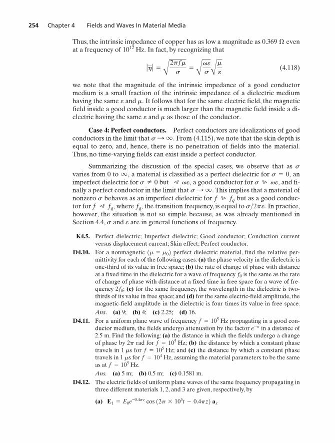
(a) (b) (c) (d)
FIGURE 4.1
Energy band diagrams for different cases: (a) and (d) conductor; (b) dielectric; and(c) semiconductor.
the nucleus upon the application of an electric field. Not taking part in thisbonding mechanism are the free, or conduction, electrons. These electrons areconstantly under thermal agitation, being released from the parent atom at onepoint and recaptured at another point. In the absence of an applied electricfield, their motion is completely random; that is, the average thermal velocity ona macroscopic scale is zero, so that there is no net current and the electron cloudmaintains a fixed position.When an electric field is applied, an additional veloc-ity is superimposed on the random velocities, thereby causing a drift of the av-erage position of the electrons along the direction opposite to that of theelectric field. This process is known as conduction. In certain materials, a largenumber of electrons may take part in this process.These materials are known asconductors. In certain other materials, only very few or a negligible number ofelectrons may participate in conduction. These materials are known asdielectrics, or insulators. A class of materials for which conduction occurs notonly by electrons but also by another type of carriers known as holes—vacan-cies created by detachment of electrons due to breaking of covalent bonds withother atoms—is intermediate to that of conductors and dielectrics. These mate-rials are called semiconductors.
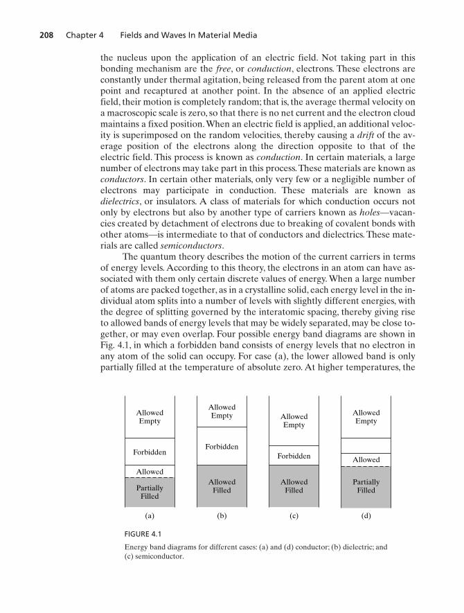
The quantum theory describes the motion of the current carriers in termsof energy levels. According to this theory, the electrons in an atom can have as-sociated with them only certain discrete values of energy. When a large numberof atoms are packed together, as in a crystalline solid, each energy level in the in-dividual atom splits into a number of levels with slightly different energies, withthe degree of splitting governed by the interatomic spacing, thereby giving riseto allowed bands of energy levels that may be widely separated, may be close to-gether, or may even overlap. Four possible energy band diagrams are shown inFig. 4.1, in which a forbidden band consists of energy levels that no electron inany atom of the solid can occupy. For case (a), the lower allowed band is onlypartially filled at the temperature of absolute zero. At higher temperatures, the
RaoCh04v3.qxd 12/18/03 3:49 PM Page 208
4.1 Conductors and Semiconductors 209
electron population in the band spreads out somewhat, but only very few elec-trons reach higher energy levels.Thus, since there are many unfilled levels in thesame band, it is possible to increase the energy of the system by moving the elec-trons to these unoccupied levels very easily by the application of an electricfield, thereby resulting in drift of the electrons. The material is then classified asa conductor. For cases (b) and (c), the lower band is completely filled, whereasthe next-higher band is completely empty at the temperature of absolute zero. Ifthe width of the forbidden band is very large as in (b), the situation at normaltemperatures is essentially the same as at absolute zero, and, hence, there are noneighboring empty energy levels for the electrons to move. The only way forconduction to take place is for the electrons in the filled band to get excited andmove to the next higher band. But this is very difficult to achieve with reason-able electric fields, and the material is then classified as a dielectric. Only by sup-plying a very large amount of energy can an electron be excited to move fromthe lower band to the higher band, where it has neighboring empty levels avail-able for causing conduction.The dielectric is said to break down under such con-ditions. If, on the other hand, the width of the forbidden band in which the Fermilevel lies is not too large, as in (c), some of the electrons in the lower band moveinto the upper band at normal temperatures, so that conduction can take placeunder the influence of an electric field, not only in the upper band, but also inthe lower band because of the vacancies (holes) left by the electrons that movedinto the upper band. The material is then classified as a semiconductor. A semi-conductor crystal in pure form is known as an intrinsic semiconductor.The prop-erties of an intrinsic crystal can be altered by introducing impurities into it. Thecrystal is then said to be an extrinsic semiconductor. For case (d), two allowedbands overlap; one or both of the bands is only partially filled and the situationcorresponds to a conductor.
In the foregoing discussion, we classified materials on the basis of theirability to permit conduction of electrons under the application of an externalelectric field. For conductors, we are interested in knowing about the relation-ship between the drift velocity of the electrons and the applied electric field,since the predominant process is conduction. But for collisions with the atomiclattice, the electric field continuously accelerates the electrons in the directionopposite to it as they move about at random. Collisions with the atomic lattice,however, provide the frictional mechanism by means of which the electrons losesome of the momentum gained between collisions. The net effect is as thoughthe electrons drift with an average drift velocity under the influence of theforce exerted by the applied electric field and an opposing force due to the fric-tional mechanism. This opposing force is proportional to the momentum of theelectron and inversely proportional to the average time between collisions.Thus, the equation of motion of an electron is given by
(4.1)
where e and m are the charge and mass of an electron.
m
dvd
dt= eE -
mvd
t
t
vd,
RaoCh04v3.qxd 12/18/03 3:49 PM Page 209
210 Chapter 4 Fields and Waves In Material Media
Rearranging (4.1), we have
(4.2)
For the sudden application of a constant electric field at the solutionfor (4.2) is given by
(4.3)
where we have evaluated the arbitrary constant of integration by using the ini-tial condition that at The values of for typical conductors such ascopper are of the order of so that the exponential term on the right sideof (4.3) decays to a negligible value in a time much shorter than that of practicalinterest. Thus, neglecting this term, we have
(4.4)
and the drift velocity is proportional in magnitude and opposite in direction tothe applied electric field, since the value of e is negative.
In fact, since we can represent a time-varying field as a superposition ofstep functions starting at appropriate times, the exponential term in (4.3) maybe neglected as long as the electric field varies slowly compared to For fieldsvarying sinusoidally with time, this means that as long as the period T of the si-nusoidal variation is several times the value of or the radian frequency
the drift velocity follows the variations in the electric field. Sincethis condition is satisfied even at frequencies up to several hundred
gigahertz (a gigahertz is ). Thus, for all practical purposes, we can assumethat
(4.5)
Now, we define the mobility, of the electron as the ratio of the magni-tudes of the drift velocity and the applied electric field. Then we have
(4.6)
and
(4.7a)
For values of typically of the order of we note by substituting for and m on the right side of (4.6) that the electron mobilities are of the order of
Alternative units for the mobility are square meters per volt-sec-ond. In semiconductors, conduction is due not only to the movement of elec-trons, but also to the movement of holes.We can define the mobility of a holemh
10-3 C-s>kg.
ƒe ƒ10-14 s,t
vd = -me E for electrons
me =ƒvd ƒƒE ƒ
=ƒe ƒtm
me,
vd =etm
E
109 Hz1>t L 1014,v � 2p>t, t,
t.
vd =etm
E0
10-14 s,tt = 0.vd = 0
vd =etm
E0 -etm
E0 e-t>t
t = 0,E0
m
dvd
dt+
mt
vd = eE
Mobility
RaoCh04v3.qxd 12/18/03 3:49 PM Page 210
4.1 Conductors and Semiconductors 211
Conductioncurrent
similarly to as the ratio of the drift velocity of the hole to the applied electricfield. Thus, we have
(4.7b)
Note from (4.7b) that conduction of a hole takes place along the direction ofthe applied electric field, since a hole is a vacancy created by the removal ofan electron and, hence, a hole movement is equivalent to the movement of apositive charge of value equal to the magnitude of the charge of an electron.In general, the mobility of holes is lower than the mobility of electrons fora particular semiconductor. For example, for silicon, the values of and are and respectively. Semiconductors are denotedn-type or p-type, depending on whether the conduction is predominantly due tothe movement of electrons or holes.
The drift of electrons in a conductor and that of electrons and holes in asemiconductor is equivalent to a current flow. This current is known as theconduction current. The conduction current density may be obtained in the fol-lowing manner. If there are free electrons per cubic meter of the material,then the amount of charge passing through an infinitesimal area normalto the drift velocity at a point in the material in a time is given by
(4.8)
The current flowing across is given by
(4.9)
The magnitude of the current density at the point is the ratio of to in thelimit tends to zero, and the direction is opposite to that of Thus, the con-duction current density resulting from the drift of electrons in the conductoris given by
(4.10)
Substituting for from (4.7a), we have
(4.11)
Defining a quantity as
(4.12)
we obtain the simple and important relationship between and E:
(4.13)
The quantity is known as the electrical conductivity of the material, and (4.13)is known as Ohm’s law valid at a point. We shall show later that the well-known
s
Jc = sE
Jc
s = me Ne ƒe ƒ
s
Jc = me Ne ƒe ƒE
vd
Jc = -Ne ƒe ƒvd
Jc
vd.¢S¢S¢I
¢I =ƒ ¢Q ƒ¢t
= Ne ƒe ƒvd ¢S
¢S¢I
¢Q = Ne e1¢S21vd ¢t2¢t
¢S¢QNe
0.048 m2>V-s,0.135 m2>V-smhme
vd = mh E for holes
me
Conductivity
RaoCh04v3.qxd 12/18/03 3:49 PM Page 211
212 Chapter 4 Fields and Waves In Material Media
Solid Dielectrics
SemiconductorsExtrinsic
Intrinsic
Metallic Conductors
0 5 10�5�10�15�20log10 s, S/m
FIGURE 4.2
Ranges of conductivities for conductors, semiconductors, and dielectrics.
Ohm’s law in circuit theory follows from it. In a semiconductor, the current den-sity is the sum of the contributions due to the drifts of electrons and holes. If thedensities of holes and electrons are and respectively, the conduction cur-rent density is given by
(4.14)
Thus, the conductivity of a semiconducting material is given by
(4.15a)
For an intrinsic semiconductor, so that (4.15a) reduces to
(4.15b)
The units of conductivity are orampere/volt-meter, also commonly known as siemens per meter (S/m), where asiemen is an ampere per volt. The ranges of conductivities for conductors, semi-conductors, and dielectrics are shown in Fig. 4.2. Values of conductivities for afew materials are listed in Table 4.1.The constant values of conductivities do notimply that the conduction current density is proportional to the applied electricfield intensity for all values of current density and field intensity. However, therange of current densities for which the material is linear, that is, for which theconductivity is a constant, is very large for conductors.
In considering electromagnetic wave propagation in conducting media,the conduction current density given by (4.13) must be employed for the cur-rent density term on the right side of Ampere’s circuital law. Thus, Maxwell’scurl equation for H for a conducting medium is given by
For illustrating the surface charge formation at the boundary of a conductor placedin a static electric field.
We shall use this equation in Sec. 4.4 to obtain the solution for sinusoidallytime-varying uniform plane waves in a material medium.
Let us now consider a conductor placed in a static electric field, as shownin Fig. 4.3(a).The free electrons in the conductor move opposite to the directionlines of the electric field. If there is a way in which the flow of electrons can becontinued to form a closed circuit, then a continuous flow of current takes place.Since the conductor is bounded by free space, the electrons are held at theboundary from moving further. Thus, a negative surface charge forms on theboundary, accompanied by an equal amount of positive surface charge, asshown in Fig. 4.3(b), since the conductor as a whole is neutral. The surfacecharge distribution formed in this manner produces a secondary electric fieldwhich, together with the applied electric field, makes the field inside the con-ductor zero. We shall illustrate the computation of the surface charge densitiesby means of a simple example.
Conductor ina staticelectric field
RaoCh04v3.qxd 12/18/03 3:49 PM Page 213
214 Chapter 4 Fields and Waves In Material Media
�
�
�
�
�
�
�
�
�
�
�
�
�
�
�
�
�
�
�
�
(c)
z � d
z � 0
rS � �e0E0
rS � �e0E0
rS � e0E0
rS � e0E0
�
�
�
�
�
�
�
�
�
�
(a)
z � d
z � 0
rS � �e0E0
rS � e0E0
E0az
�
�
�
�
�
�
�
�
�
�
(b)
z � d
z � 0
rS0
�rS0
rS0
e0azE � �
FIGURE 4.4
(a) Infinite plane slab conductor in a uniform applied field. (b) Induced surface charge at theboundaries of the conductor and the secondary field. (c) Sum of the applied and the secondary fields.
Example 4.1 Plane conducting slab in a uniform static electric field
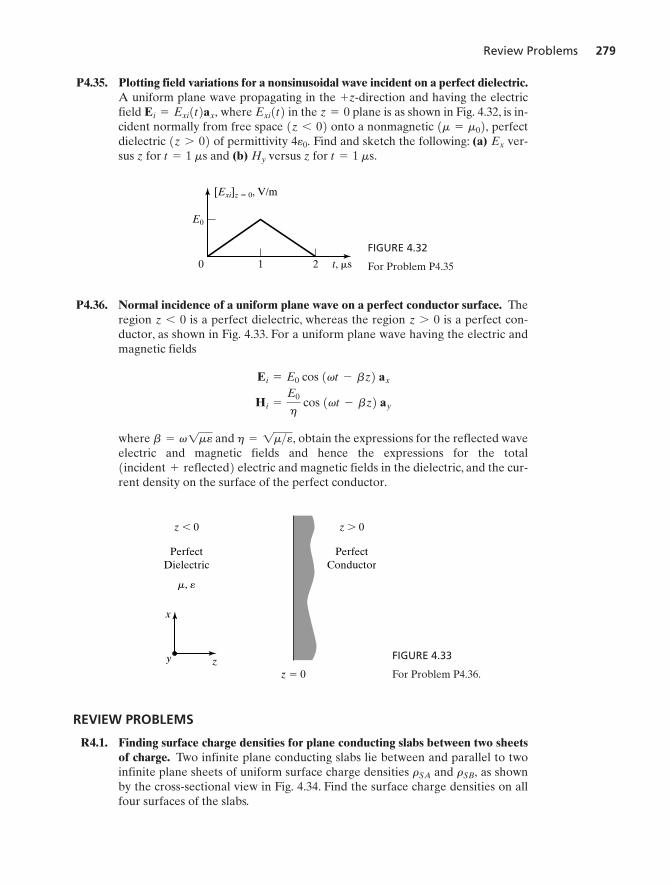
Let us consider an infinite plane conducting slab of thickness d occupying the region be-tween and and in a uniform electric field produced by two infiniteplane sheets of equal and opposite uniform charge densities on either side of the slab, asshown in Fig. 4.4(a).We wish to find the charge densities induced on the surfaces of the slab.
Since the applied electric field is uniform and is directed along the z-direction, anegative charge of uniform density forms on the surface due to the accumulationof free electrons at that surface. A positive charge of equal and opposite uniform densityforms on the surface due to a deficiency of electrons at that surface. Let these sur-face charge densities be and respectively. To satisfy the property that the fieldin the interior of the conductor is zero, the secondary field produced by the surfacecharges must be equal and opposite to the applied field; that is, it must be equal to
Now, each surface charge produces a field intensity directed normally from it andhaving a magnitude times the charge density so that the field due to the two sur-face charges together is equal to inside the conductor and zero outside theconductor, as shown in Fig. 4.4(b). Thus, for zero field inside the conductor,
or
The field outside the conductor remains the same as the applied field since the sec-ondary field in that region due to the surface charges is zero.The induced surface charge
rS0 = e0 E0
-
rS0
e0 az = -E0 az
-1rS0>e02az
1>2e0
-E0 az.
rS0,-rS0
z = d
z = 0
E = E0 azz = dz = 0
RaoCh04v3.qxd 12/18/03 3:49 PM Page 214
4.1 Conductors and Semiconductors 215
lA
I
V
E
FIGURE 4.5
For the derivation of Ohm’s law in circuittheory.
distribution and the fields inside and outside the conductor are shown in Fig. 4.4(c). Inthe general case, the induced surface charge produces a secondary field outside the con-ductor also, thereby changing the applied field.
Returning now to (4.13), we shall show that the well-known Ohm’s law incircuit theory follows from it. To do this, let us consider a bar of conducting ma-terial of conductivity length l, and uniform cross-sectional area A, betweenthe ends of which a voltage V is applied, as shown in Fig. 4.5.The voltage sets upan electric field directed along the length of the conductor, thereby giving riseto conduction current. Assuming, for simplicity, uniformity of the electric field,the voltage between the two ends of the conductor is given by the electric fieldintensity times the length of the conductor, that is,
(4.17)
Then from (4.13) and (4.17), the conduction current density magnitude is given by
(4.18)
Assuming uniformity of the field and hence of the conduction current density inthe cross-sectional area of the conductor, we then obtain the conduction currentto be
(4.19)
Upon rearrangement, we get
(4.20)
which is in the form of the familiar Ohm’s law,
(4.21)
From (4.20), the resistance R of the conducting bar can now be identified as
(4.22)
the units of R being ohms.
R =l
sA
V = IR
V = I l
sA
I = Jc A =sA
l V
Jc = sE =sV
l
V = El
s,
Ohm’s law,resistance
RaoCh04v3.qxd 12/18/03 3:49 PM Page 215
216 Chapter 4 Fields and Waves In Material Media
y
x
z
�Hole
EH
FHFm
v
B
I
I
FIGURE 4.6
For illustrating the Hall effectphenomenon.
We shall conclude this section with a discussion of the Hall effect, an im-portant phenomenon employed in the determination of charge densities in con-ducting and semiconducting materials, as well as in other techniques such as themeasurement of fluid flow using electromagnetic flow meters. Let us considerthe p-type semiconducting material in the form of a rectangular bar shown inFig. 4.6, in which holes drift in the x-direction with a velocity due to anapplied voltage between the two ends of the bar. If a magnetic field isapplied in a perpendicular direction, then the drifting holes will experience amagnetic force that deflects them in the or This de-flection of holes toward the establishes an electric field
in the material, resulting in the development of a voltage betweenthe two sides of the bar. This phenomenon is known as the Hall effect, and thevoltage developed is known as the Hall voltage. Were it not for the establish-ment of the Hall electric field, the holes would continually deflect toward the
as they drift in the x-direction. The Hall electric field exerts forceon the holes in the which in the steady-state balances exactly
the magnetic force in the so that the net y-directed force iszero. According to the Lorentz force equation (1.89), the Hall electric field thatachieves this balance is given by
(4.23)
or By using this result, the hole density can be computed from ameasurement of the Hall voltage for known values of the magnetic field the current I, and the cross-sectional dimensions of the bar. If the material isn-type instead of p-type, then the charge carriers are electrons, and v would bein the The deflection of the charge carriers will still be toward the
since the charge is negative. This results in an electric field in the-y-direction-x-direction.
Bz,Ey = vx Bz.
= q1Ey - vx Bz2ay = 0
q1EH + v � B2 = q1Ey ay + vx ax � Bz az2
-y-directionFm
+y-direction,FH
-y-direction
EH = Ey ay
-y-direction-ay-direction.ax � azFm
B = Bz az
v = vx ax
Hall effect
RaoCh04v3.qxd 12/18/03 3:49 PM Page 216
4.2 Dielectrics 217
rSA
rSB
1
2FIGURE 4.7
For Problem D4.2.
and hence in a Hall voltage of opposite polarity to that in the caseof the p-type material. Thus, the polarity of the Hall voltage can be used to de-termine if the charge carriers are holes or electrons.
K4.1. Conduction; Conduction current density; Conductivity; Ohm’s law; Conductorin a static electric field; Resistance; Hall effect.
D4.1. Find the magnitude of the electric field intensity required to establish the flowof a conduction current of 0.1 A across an area of normal to the field foreach of the following cases: (a) in copper; (b) in an intrinsic semiconductor ma-terial with electron and hole mobilities of and re-spectively, and electron and hole densities of and (c) in ametallic wire of circular cross section of radius 1 mm, length 1 m, and resistance1 ohm.Ans. (a) (b) 471.1 V/m; (c) 3.14 mV/m.
D4.2. An infinite plane conducting slab lies between, and parallel to, two infiniteplane sheets of charge of uniform surface charge densities and asshown by the cross-sectional view in Fig. 4.7. Find the surface charge densitieson the two surfaces of the slab: (a) and (b)Ans. (a) (b)
4.2 DIELECTRICS
In the preceding section, we learned that conductors are characterized by anabundance of conduction, or free, electrons that give rise to conduction currentunder the influence of an applied electric field. In this section, we turn our at-tention to dielectric materials in which the bound electrons are predominant.Under the application of an external electric field, the bound electrons of anatom are displaced such that the centroid of the electron cloud is separatedfrom the centroid of the nucleus. The atom is then said to be polarized, therebycreating an electric dipole, as shown in Fig. 4.8(a). This kind of polarization iscalled electronic polarization.The schematic representation of an electric dipoleis shown in Fig. 4.8(b). The strength of the dipole is defined by the electric di-pole moment p given by
(4.24)
where d is the vector displacement between the centroids of the positive andnegative charges, each of magnitude Q coulombs.
p = Qd
121rSA - rSB2.1
21rSB - rSA2;rS2.rS1
rSB,rSA
17.24 mV>m;
2.5 * 1013 cm-3;1700 cm2>V-s,3600 cm2>V-s
1 cm2
-y-direction
Polarization,electric dipole
RaoCh04v3.qxd 12/18/03 3:49 PM Page 217
218 Chapter 4 Fields and Waves In Material Media
(a) (b)
�
�
�
�
E d
Q
�QFIGURE 4.8
(a) Electric dipole. (b) Schematic representation of anelectric dipole.
�
�
Q
QE
�Q
�QE
E
FIGURE 4.9
Torque acting on an electric dipole in an externalelectric field.
In certain dielectric materials, polarization may exist in the molecularstructure of the material even under the application of no external electric field.The polarization of individual atoms and molecules, however, is randomly ori-ented, and hence the net polarization on a macroscopic scale is zero. The appli-cation of an external field results in torques acting on the microscopic dipoles,as shown in Fig. 4.9, to convert the initially random polarization into a partiallycoherent one along the field, on a macroscopic scale.This kind of polarization isknown as orientational polarization.A third kind of polarization, known as ionicpolarization, results from the separation of positive and negative ions in mole-cules formed by the transfer of electrons from one atom to another in the mole-cule. Certain materials exhibit permanent polarization, that is, polarization evenin the absence of an applied electric field. Electrets, when allowed to solidify inthe applied electric field, become permanently polarized, and ferroelectric ma-terials exhibit spontaneous, permanent polarization.
On a macroscopic scale, we define a vector P, called the polarization vec-tor, as the electric dipole moment per unit volume.Thus, if N denotes the numberof molecules per unit volume of the material, then there are molecules ina volume and
(4.25)P =1
¢v aN ¢v
j = 1pj = Np
¢vN ¢v
RaoCh04v3.qxd 12/18/03 3:49 PM Page 218
4.2 Dielectrics 219
where p is the average dipole moment per molecule. The units of P areor coulombs per square meter. It is found that for many
dielectric materials, the polarization vector is related to the electric field E inthe dielectric in the simple manner given by
(4.26)
where a dimensionless parameter, is known as the electric susceptibility. Thequantity is a measure of the ability of the material to become polarized anddiffers from one dielectric to another.
When a dielectric material is placed in an electric field, the induced dipolesproduce a secondary electric field such that the resultant field, that is, the sum ofthe originally applied field and the secondary field, and the polarization vectorsatisfy (4.26). We shall illustrate this by means of a simple example.
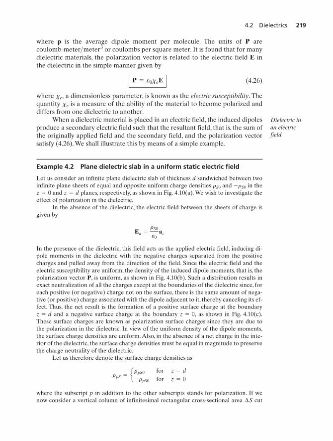
Example 4.2 Plane dielectric slab in a uniform static electric field
Let us consider an infinite plane dielectric slab of thickness d sandwiched between twoinfinite plane sheets of equal and opposite uniform charge densities and in the
and planes, respectively, as shown in Fig. 4.10(a). We wish to investigate theeffect of polarization in the dielectric.
In the absence of the dielectric, the electric field between the sheets of charge isgiven by
In the presence of the dielectric, this field acts as the applied electric field, inducing di-pole moments in the dielectric with the negative charges separated from the positivecharges and pulled away from the direction of the field. Since the electric field and theelectric susceptibility are uniform, the density of the induced dipole moments, that is, thepolarization vector P, is uniform, as shown in Fig. 4.10(b). Such a distribution results inexact neutralization of all the charges except at the boundaries of the dielectric since, foreach positive (or negative) charge not on the surface, there is the same amount of nega-tive (or positive) charge associated with the dipole adjacent to it, thereby canceling its ef-fect. Thus, the net result is the formation of a positive surface charge at the boundary
and a negative surface charge at the boundary as shown in Fig. 4.10(c).These surface charges are known as polarization surface charges since they are due tothe polarization in the dielectric. In view of the uniform density of the dipole moments,the surface charge densities are uniform. Also, in the absence of a net charge in the inte-rior of the dielectric, the surface charge densities must be equal in magnitude to preservethe charge neutrality of the dielectric.
Let us therefore denote the surface charge densities as
where the subscript p in addition to the other subscripts stands for polarization. If wenow consider a vertical column of infinitesimal rectangular cross-sectional area cut¢S
rpS = erpS0 for z = d
-rpS0 for z = 0
z = 0,z = d
Ea =rS0
e0 az
z = dz = 0-rS0rS0
xe
xe,
P = e0xe E
coulomb-meter>meter3
Dielectric inan electricfield
RaoCh04v3.qxd 12/18/03 3:49 PM Page 219
220 Chapter 4 Fields and Waves In Material Media
� �� �
(d)
rpS0 �S
�rpS0 �S
� �� �
d
(b)
�
�
�
�
�
�
�
�
�
�
�
�
�
�
�
�
�
�
�
�
�
�
�
�
�
�
�
�
�
�
�
�
�
�
�
�
�
�
(a)
z � d
z � 0
rS0
�rS0
xe � xe0
Ea
(c)
z � d
z � 0rpS � �rpS0
rpS � rpS0
� � � �
� � � �
(e)
�
�
�
�
�
�
�
�
�
�
�
�
�
� � � �
�
� � � �
Et
FIGURE 4.10
For investigating the effect of polarization induced in a dielectric material sandwiched between twoinfinite plane sheets of charge.
out from the dielectric, as shown in Fig. 4.10(d), the equal and opposite surface chargesmake the column appear as a dipole of moment On the other hand, writing
(4.27)
where is a constant in view of the uniformity of the induced polarization, the dipolemoment of the column is equal to P times the volume of the column, or Equating the dipole moments computed in the two different ways, we have
rpS0 = P0
P01d ¢S2az.P0
P = P0 az
1rpS0 ¢S2daz.
RaoCh04v3.qxd 12/18/03 3:49 PM Page 220
4.2 Dielectrics 221
Thus, we have related the surface charge density to the magnitude of the polariza-tion vector. Now, the surface charge distribution produces a secondary field given by
Denoting the total field in the dielectric to be we have
(4.28)
But from (4.26),
(4.29)
Substituting (4.27) and (4.28) into (4.29), we obtain
or
(4.30)
Thus, the polarization surface charge densities are given by
(4.31)
and the electric field intensity in the dielectric is
(4.32)
as shown in Fig. 4.10(e).
Let us now consider the case of the infinite plane current sheet of Fig. 3.14,radiating uniform plane waves, except that now the space on either side of thecurrent sheet is a dielectric material instead of free space. The electric field inthe medium induces polarization. The polarization in turn acts together withother factors to govern the behavior of the electromagnetic field. For the caseunder consideration, the electric field is entirely in the x-direction and uniformin x and y. Thus the induced dipoles are all oriented in the x-direction, on amacroscopic scale, with the dipole moment per unit volume given by
(4.33)
where is understood to be a function of z and t.Ex
P = Px ax = e0xe Ex ax
Et =rS0
e011 + xe02 az
rpS = d xe0rS0
1 + xe0for z = d
-
xe0rS0
1 + xe0for z = 0
P0 =xe0rS0
1 + xe0
P0 = xe01rS0 - P02
P = e0xe0 Et
Et = Ea + Es =rS0
e0 az -
P0
e0 az
Et,
Es = c -
rpS0
e0 az = -
P0
e0 az for 0 6 z 6 d
0 otherwise
Es
RaoCh04v3.qxd 12/18/03 3:49 PM Page 221
222 Chapter 4 Fields and Waves In Material Media
If we now consider an infinitesimal surface of area parallel to theyz plane, we can write associated with that infinitesimal area to be equal to
where is a constant.The time history of the induced dipoles associ-ated with that area can be sketched for one complete period of the currentsource, as shown in Fig. 4.11. In view of the cosinusoidal variation of the elec-tric field with time, the dipole moment of the individual dipoles varies in a cos-inusoidal manner with maximum strength in the positive x direction at decreasing sinusoidally to zero strength at and then reversing to thenegative x direction, increasing to maximum strength in that direction at and so on.
t = p>v,t = p>2v t = 0,
E0E0 cos vt,Ex
¢y ¢z
E
vt � 0
� ��
� ��
� �� �
��
���
�� �
���
� ��
E
vt � p
� ��
� ��
� �� �
��
���
�� �
vt � 2p
���
� ��
E
� �
� �� ���
��
� �
��
� �
vt � p4
E
� �
� �� ���
��
� �
��
� �
vt � 3p4
E
� �
� �� ���
��
� �
��
� �
vt � 7p4
vt � 3p2
vt � 5p4
vt � p2
�z
�y
E
� �
� �� ���
��
� �
��
� �
xz
y
E
� ��
� ��
� �� �
��
���
�� �
���
� ��
FIGURE 4.11
Time history of induced electric dipoles in a dielectric material under the influence of asinusoidally time-varying electric field.
RaoCh04v3.qxd 12/18/03 3:49 PM Page 222
4.2 Dielectrics 223
d
�z
�y
Q2 � �Q1
Q1 � e0xeE0 cos vt �y�z
FIGURE 4.12
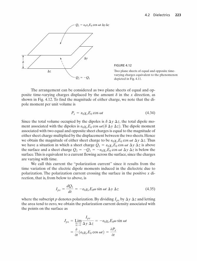
Two plane sheets of equal and opposite time-varying charges equivalent to the phenomenondepicted in Fig. 4.11.
The arrangement can be considered as two plane sheets of equal and op-posite time-varying charges displaced by the amount in the x direction, asshown in Fig. 4.12. To find the magnitude of either charge, we note that the di-pole moment per unit volume is
(4.34)
Since the total volume occupied by the dipoles is the total dipole mo-ment associated with the dipoles is The dipole momentassociated with two equal and opposite sheet charges is equal to the magnitude ofeither sheet charge multiplied by the displacement between the two sheets. Hencewe obtain the magnitude of either sheet charge to be Thuswe have a situation in which a sheet charge is abovethe surface and a sheet charge is below thesurface.This is equivalent to a current flowing across the surface, since the chargesare varying with time.
We call this current the “polarization current” since it results from thetime variation of the electric dipole moments induced in the dielectric due topolarization. The polarization current crossing the surface in the positive x di-rection, that is, from below to above, is
(4.35)
where the subscript p denotes polarization. By dividing by and lettingthe area tend to zero, we obtain the polarization current density associated withthe points on the surface as
=00t
1e0xe E0 cos vt2 =0Px
0t
Jpx = Lim¢y:0¢z:0
Ipx
¢y ¢z= -e0xe E0v sin vt
¢y ¢zIpx
Ipx =dQ1
dt= -e0xe E0v sin vt ¢y ¢z
Q2 = -Q1 = -e0xe E0 cos vt ¢y ¢zQ1 = e0xe E0 cos vt ¢y ¢z
e0xe E0 cos vt ¢y ¢z.
e0xe E0 cos vt1d ¢y ¢z2.d ¢y ¢z,
Px = e0xe E0 cos vt
d
RaoCh04v3.qxd 12/18/03 3:49 PM Page 223
224 Chapter 4 Fields and Waves In Material Media
or
(4.36)
Although we have deduced this result by considering the special case of the in-finite plane current sheet, it is valid in general.
In considering electromagnetic wave propagation in a dielectric medium,the polarization current density given by (4.36) must be included with the cur-rent density term on the right side of Ampere’s circuital law. Thus consideringAmpere’s circuital law in differential form for the general case given by (3.21),we have
(4.37)
In order to make (4.37) consistent with the corresponding equation for freespace given by (3.21), we now revise the definition of the displacement vector Dto read as
(4.38)
Substituting for P by using (4.26), we obtain
(4.39)
or
(4.40)
where we define
(4.41)
and
(4.42)
The quantity is known as the relative permittivity or dielectric constant of thedielectric, and is the permittivity of the dielectric. The permittivity takes intoaccount the effects of polarization, and there is no need to consider them whenwe use for for The relative permittivity is an experimentally measurableparameter. Its values for several dielectric materials are listed in Table 4.2.
e0!e
ee
er
e = e0er
er = 1 + xe
D = eE
= e0er E= e011 + xe2E
D = e0 E + e0xe E
D = e0 E + P
= J +00t
1e0 E + P2 = J +
0P0t
+00t
1e0 E2 � � H = J + Jp +
00t
1e0 E2
Jp =0P0t
RaoCh04v3.qxd 12/18/03 3:49 PM Page 224
4.2 Dielectrics 225
Table 4.2 Relative Permittivities of Some Materials
Relative RelativeMaterial Permittivity Material Permittivity
Returning now to Example 4.2, we observe that in the absence of the di-electric between the sheets of charge,
(4.43a)
(4.43b)
since P is equal to zero. In the presence of the dielectric between the sheets ofcharge,
(4.44a)
(4.44b)
Thus, the D fields are the same in both cases, independent of the permittivity ofthe medium, whereas the expressions for the E fields differ in the permittivities,that is, with replaced by The situation in general is, however, not so simplebecause the dielectric alters the original field distribution. In the case of Exam-ple 4.2, the geometry is such that the original field distribution is not altered bythe dielectric.Also in the general case, the situation is equivalent to having a po-larization volume charge inside the dielectric in addition to polarization surfacecharges on its boundaries.
The nature of (4.13), which is characteristic of conductors, and of (4.40),which is characteristic of dielectrics, implies that in the case of conductors andD in the case of dielectrics are in the same direction as that of E. Such materialsare said to be isotropic materials. For anisotropic materials, this is not necessari-ly the case. To explain, we shall consider anisotropic dielectric materials. Then Dis not in general in the same direction as that of E. This arises because the in-duced polarization is such that the polarization vector P is not necessarily in thesame direction as that of E. In fact, the angle between the directions of the ap-plied E and the resulting P depends on the direction of E. The relationship be-tween D and E is then expressed in the form of a matrix equation as
(4.45)CDx
Dy
Dz
S = C exx exy exz
eyx eyy eyz
ezx ezy ezz
S CEx
Ey
Ez
S
Jc
e.e0
D = eE = rS0 az
E = Et =rS0
e011 + xe02 az =rS0
e az
D = e0 Ea = rS0 az
E = Ea =rS0
e0 az
Anisotropicdielectricmaterials
RaoCh04v3.qxd 12/18/03 3:49 PM Page 225
226 Chapter 4 Fields and Waves In Material Media
Thus, each component of D is in general dependent on each component of E.The square matrix in (4.45) is known as the permittivity tensor of the anisotrop-ic dielectric.
Although D is not in general parallel to E for anisotropic dielectrics, thereare certain polarizations of E for which D is parallel to E. These are said to cor-respond to the characteristic polarizations, where the word polarization hererefers to the direction of the field, not to the creation of electric dipoles. Weshall consider an example to investigate the characteristic polarizations.
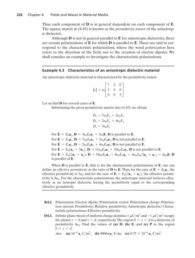
Example 4.3 Characteristics of an anisotropic dielectric material
An anisotropic dielectric material is characterized by the permittivity tensor
Let us find D for several cases of E.Substituting the given permittivity matrix into (4.45), we obtain
For D is parallel to E.For D is not parallel to E.For D is not parallel to E.For D is not parallel to E.For Dis parallel of E.
When D is parallel to E, that is, for the characteristic polarizations of E, one candefine an effective permittivity as the ratio of D to E. Thus, for the case of theeffective permittivity is and for the case of the effective permit-tivity is For the characteristic polarizations, the anisotropic material behaves effec-tively as an isotropic dielectric having the permittivity equal to the correspondingeffective permittivity.
D4.3. Infinite plane sheets of uniform charge densities and occupythe planes and respectively.The region is a dielectric ofpermittivity Find the values of (a) D, (b) E, and (c) P in the region
Ans. (a) (b) (c) 0.75 * 10-6 az C>m2.9000paz V>m;10-6 az C>m2;0 6 z 6 d.
4e0.0 6 z 6 dz = d,z = 0
-1 mC>m21 mC>m2
8e0.E = E012ax + ay2,3e0,
E = E0 az,
E = E012ax + ay2, D = 16e0 E0 ax + 8e0 E0 ay = 8e0 E012ax + ay2 = 8e0 E;
E = E01ax + 2ay2, D = 11e0 E0 ax + 10e0 E0 ay;E = E0 ay, D = 2e0 E0 ax + 4e0 E0 ay;E = E0 ax, D = 7e0 E0 ax + 2e0 E0 ay;E = E0 az, D = 3e0 E0 az = 3e0 E;
Dz = 3e0 Ez
Dy = 2e0 Ex + 4e0 Ey
Dx = 7e0 Ex + 2e0 Ey
[e] = e0C7 2 02 4 00 0 3
S
RaoCh04v3.qxd 12/18/03 3:49 PM Page 226
4.3 Magnetic Materials 227
(a)
an I
(b)
Iin Iout
FIGURE 4.13
Schematic representation of a magneticdipole as seen from (a) along its axis and(b) a point in its plane.
D4.4. For an anisotropic dielectric material characterized by the D to E relationship
find the value of the effective relative permittivity for each of the followingelectric field intensities corresponding to the characteristic polarizations:
(b) and (c)Ans. (a) 9; (b) 4; (c) 9.
4.3 MAGNETIC MATERIALS
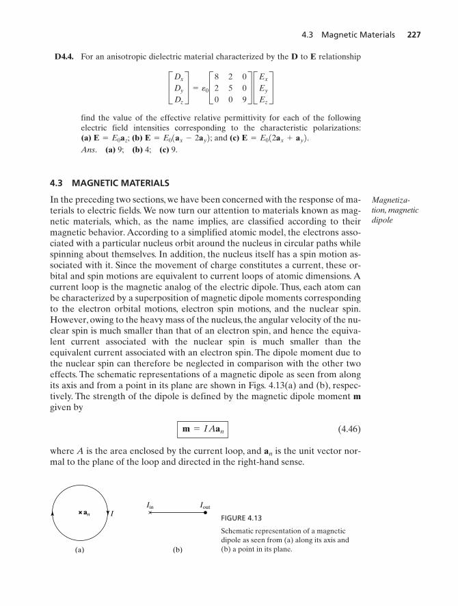
In the preceding two sections, we have been concerned with the response of ma-terials to electric fields. We now turn our attention to materials known as mag-netic materials, which, as the name implies, are classified according to theirmagnetic behavior. According to a simplified atomic model, the electrons asso-ciated with a particular nucleus orbit around the nucleus in circular paths whilespinning about themselves. In addition, the nucleus itself has a spin motion as-sociated with it. Since the movement of charge constitutes a current, these or-bital and spin motions are equivalent to current loops of atomic dimensions. Acurrent loop is the magnetic analog of the electric dipole. Thus, each atom canbe characterized by a superposition of magnetic dipole moments correspondingto the electron orbital motions, electron spin motions, and the nuclear spin.However, owing to the heavy mass of the nucleus, the angular velocity of the nu-clear spin is much smaller than that of an electron spin, and hence the equiva-lent current associated with the nuclear spin is much smaller than theequivalent current associated with an electron spin. The dipole moment due tothe nuclear spin can therefore be neglected in comparison with the other twoeffects. The schematic representations of a magnetic dipole as seen from alongits axis and from a point in its plane are shown in Figs. 4.13(a) and (b), respec-tively. The strength of the dipole is defined by the magnetic dipole moment mgiven by
(4.46)
where A is the area enclosed by the current loop, and is the unit vector nor-mal to the plane of the loop and directed in the right-hand sense.
an
m = IAan
E = E012ax + ay2.E = E01ax - 2ay2;(a) E = E0 az;
CDx
Dy
Dz
S = e0C8 2 02 5 00 0 9
S CEx
Ey
Ez
S
Magnetiza-tion, magneticdipole
RaoCh04v3.qxd 12/18/03 3:49 PM Page 227
228 Chapter 4 Fields and Waves In Material Media
I
I
I d l � B
B
I d l � B
FIGURE 4.14
Torque acting on a magnetic dipolein an external magnetic field.
In many materials, the net magnetic moment of each atom is zero; that is,on the average, the magnetic dipole moments corresponding to the various elec-tronic orbital and spin motions add up to zero. An external magnetic field hasthe effect of inducing a net dipole moment by changing the angular velocities ofthe electronic orbits, thereby magnetizing the material. This kind of magnetiza-tion, known as diamagnetism, is in fact prevalent in all materials. In certain ma-terials known as paramagnetic materials, the individual atoms possess netnonzero magnetic moments even in the absence of an external magnetic field.These permanent magnetic moments of the individual atoms are, however, ran-domly oriented so that the net magnetization on a macroscopic scale is zero.Anapplied magnetic field has the effect of exerting torques on the individual per-manent dipoles, as shown in Fig. 4.14, that convert, on a macroscopic scale, theinitially random alignment into a partially coherent one along the magneticfield, that is, with the normal to the current loop directed along the magneticfield. This kind of magnetization is known as paramagnetism. Certain materialsknown as ferromagnetic, antiferromagnetic, and ferrimagnetic materials exhibitpermanent magnetization, that is, magnetization even in the absence of an ap-plied magnetic field.
On a macroscopic scale, we define a vector M, called the magnetizationvector, as the magnetic dipole moment per unit volume. Thus, if N denotes thenumber of molecules per unit volume of the material, then there are mol-ecules in a volume and
(4.47)
where m is the average dipole moment per molecule. The units of M areor amperes per meter. It is found that for many magnet-
ic materials, the magnetization vector is related to the magnetic field B in thematerial in the simple manner given by
(4.48)
where a dimensionless parameter, is known as the magnetic susceptibility.The quantity is a measure of the ability of the material to become magne-tized and differs from one magnetic material to another.
xm
xm,
M =xm
1 + xm Bm0
ampere-meter2>meter3
M =1
¢v aN ¢v
j = 1mj = Nm
¢vN ¢v
RaoCh04v3.qxd 12/18/03 3:49 PM Page 228
4.3 Magnetic Materials 229
(c)
z � d
z � 0
JmS � �JmS0ay
JmS � JmS0ay
(e)
Bt
(b)(a)
z � d
z � 0
xm � xm0
Ba
�JS0ay
JS0ay
(d)
d
�x
�y
FIGURE 4.15
For investigating the effect of magnetization induced in a magnetic material sandwiched between twoinfinite plane sheets of current.
Magneticmaterial in amagnetic field
When a magnetic material is placed in a magnetic field, the induced dipolesproduce a secondary magnetic field such that the resultant field, that is, the sumof the originally applied field and the secondary field, and the magnetization vec-tor satisfy (4.48). We shall illustrate this by means of an example.
Example 4.4 Plane magnetic material slab in a uniform static magnetic field
Let us consider an infinite plane magnetic material slab of thickness d sandwiched be-tween two infinite plane sheets of equal and opposite uniform current densities and
in the and planes, respectively, as shown in Fig. 4.15(a). We wish toinvestigate the effect of magnetization in the magnetic material.
In the absence of the magnetic material, the magnetic field between the sheets ofcurrent is given by
= m0 JS0 ax
Ba = m0 JS0 ay � az
z = dz = 0-JS0 ay
JS0 ay
RaoCh04v3.qxd 12/18/03 3:49 PM Page 229
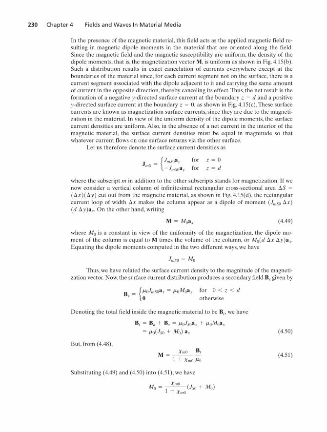
230 Chapter 4 Fields and Waves In Material Media
In the presence of the magnetic material, this field acts as the applied magnetic field re-sulting in magnetic dipole moments in the material that are oriented along the field.Since the magnetic field and the magnetic susceptibility are uniform, the density of thedipole moments, that is, the magnetization vector M, is uniform as shown in Fig. 4.15(b).Such a distribution results in exact cancelation of currents everywhere except at theboundaries of the material since, for each current segment not on the surface, there is acurrent segment associated with the dipole adjacent to it and carrying the same amountof current in the opposite direction, thereby canceling its effect.Thus, the net result is theformation of a negative y-directed surface current at the boundary and a positivey-directed surface current at the boundary as shown in Fig. 4.15(c). These surfacecurrents are known as magnetization surface currents, since they are due to the magneti-zation in the material. In view of the uniform density of the dipole moments, the surfacecurrent densities are uniform. Also, in the absence of a net current in the interior of themagnetic material, the surface current densities must be equal in magnitude so thatwhatever current flows on one surface returns via the other surface.
Let us therefore denote the surface current densities as
where the subscript m in addition to the other subscripts stands for magnetization. If wenow consider a vertical column of infinitesimal rectangular cross-sectional area
cut out from the magnetic material, as shown in Fig. 4.15(d), the rectangularcurrent loop of width makes the column appear as a dipole of moment
On the other hand, writing
(4.49)
where is a constant in view of the uniformity of the magnetization, the dipole mo-ment of the column is equal to M times the volume of the column, or Equating the dipole moments computed in the two different ways, we have
Thus, we have related the surface current density to the magnitude of the magneti-zation vector. Now, the surface current distribution produces a secondary field given by
Denoting the total field inside the magnetic material to be we have
(4.50)
But, from (4.48),
(4.51)
Substituting (4.49) and (4.50) into (4.51), we have
M0 =xm0
1 + xm0 1JS0 + M02
M =xm0
1 + xm0
Bt
m0
= m01JS0 + M02 ax
Bt = Ba + Bs = m0 JS0 ax + m0 M0 ax
Bt,
Bs = em0 JmS0 ax = m0 M0 ax for 0 6 z 6 d
0 otherwise
Bs
JmS0 = M0
M01d ¢x ¢y2ax.M0
M = M0 ax
1d ¢y2ax.1JmS0 ¢x2¢x
1¢x21¢y2¢S =
JmS = eJmS0 ay for z = 0-JmS0 ay for z = d
z = 0,z = d
RaoCh04v3.qxd 12/18/03 3:49 PM Page 230
4.3 Magnetic Materials 231
or
(4.52)
Thus, the magnetization surface current densities are given by
(4.53)
and the magnetic flux density in the magnetic material is
(4.54)
as shown in Fig. 4.15(e).
Let us now consider the case of the infinite plane current sheet of Fig. 3.14,radiating uniform plane waves, except that now the space on either side of thecurrent sheet possesses magnetic material properties in addition to dielectricproperties. The magnetic field in the medium induces magnetization. The mag-netization in turn acts together with other factors to govern the behavior of theelectromagnetic field. For the case under consideration, the magnetic field is en-tirely in the y-direction and uniform in x and y. Thus the induced dipoles are alloriented with their axes in the y-direction, on a macroscopic scale, with the di-pole moment per unit volume given by
(4.55)
where is understood to be a function of z and t.Let us now consider an infinitesimal surface of area parallel to the
yz plane and the magnetic dipoles associated with the two areas to theleft and to the right of the center of this area as shown in Fig. 4.16(a). Since isa function of z, we can assume the dipoles in the left area to have a different mo-ment than the dipoles in the right area for any given time. If the dimension of anindividual dipole is in the x direction, then the total dipole moment associatedwith the dipoles in the left area is and the total dipole mo-ment associated with the dipoles in the right area is
The arrangement of dipoles can be considered to be equivalent to two rec-tangular surface current loops as shown in Fig. 4.16 (b) with the left side currentloop having a dipole moment and the right side current loophaving a dipole moment Since the magnetic dipole momentof a rectangular surface current loop is simply equal to the product of the sur-face current and the cross-sectional area of the loop, the surface current associ-ated with the left loop is and the surface current associated withthe right loop is Thus we have a situation in which a currentequal to is crossing the area in the positive x direction, anda current equal to is crossing the same area in the negative x di-rection. This is equivalent to a net current flowing across the surface.
[My]z + ¢z>2 ¢y¢y ¢z[My]z - ¢z>2 ¢y
[My]z + ¢z>2 ¢y.[My]z - ¢z>2 ¢y
[My]z + ¢z>2 d ¢y ¢z.[My]z - ¢z>2 d ¢y ¢z
[My]z + ¢z>2 d ¢y ¢z.[My]z - ¢z>2 d ¢y ¢z
d
By
¢y ¢z¢y ¢z
By
M = Mx ay =xm
1 + xm
By
m0 ay
Bt = m011 + xm02JS0 ax
JmS = exm0 JS0 ay for z = 0-xm0 JS0 ay for z = d
M0 = xm0 JS0
RaoCh04v3.qxd 12/18/03 3:49 PM Page 231
232 Chapter 4 Fields and Waves In Material Media
B B
dd
x
z
y
x
z
y
�z2
z �
�z2
z � �z2
z � z
�z2
z � z
d
�y
d
�y
�z �z
(a)
(b)
FIGURE 4.16
(a) Induced magnetic dipoles in a magnetic material. (b) Equivalent surface current loops.
We call this current the “magnetization current,” since it results from thespace variation of the magnetic dipole moments induced in the magnetic mate-rial due to magnetization. The net magnetization current crossing the surface inthe positive x direction is
(4.56)
where the subscript m denotes magnetization. By dividing by and let-ting the area tend to zero, we obtain the magnetization current density associated
¢y ¢zImx
Imx = [My]z - ¢z>2 ¢y - [My]z + ¢z>2 ¢y
RaoCh04v3.qxd 12/19/03 12:32 PM Page 232
4.3 Magnetic Materials 233
with the points on the surface as
or
or
(4.57)
Although we have deduced this result by considering the special case of the in-finite plane current sheet, it is valid in general.
In considering electromagnetic wave propagation in a magnetic materialmedium, the magnetization current density given by (4.57) must be includedwith the current density term on the right side of Ampere’s circuital law. Thusconsidering Ampere’s circuital law in differential form for the general casegiven by (3.21), we have
(4.58)
or
(4.59)
In order to make (4.59) consistent with the corresponding equation for freespace given by (3.21), we now revise the definition of the magnetic field intensi-ty vector H to read as
(4.60)H =Bm0
- M
� � a Bm0
- Mb = J +0D0t
= J + � � M +0D0t
� �Bm0
= J + Jm +0D0t
Jm = � � M
Jmx ax = 4 ax ay az
00x
00y
00z
0 My 0
4
= -
0My
0z
Jmx = Lim¢y:0¢z:0
Imx
¢y ¢z= Lim
¢z:0
[My]z - ¢z>2 - [My]z + ¢z>2¢z
RaoCh04v3.qxd 12/18/03 3:49 PM Page 233
234 Chapter 4 Fields and Waves In Material Media
Substituting for M by using (4.48), we obtain
(4.61)
or
(4.62)
where we define
(4.63)
and
(4.64)
The quantity is known as the relative permeability of the magnetic materialand is the permeability of the magnetic material. The permeability takesinto account the effects of magnetization, and there is no need to consider themwhen we use for
Returning now to Example 4.4, we observe that in the absence of the mag-netic material between the sheets of current,
(4.65a)
(4.65b)
since M is equal to zero. In the presence of the magnetic material between thesheets of current,
(4.66a)
(4.66b)
Thus, the H fields are the same in both cases, independent of the permeability ofthe medium, whereas the expressions for the B fields differ in the permeabili-ties, that is, with replaced by The situation in general is, however, not sosimple because the magnetic material alters the original field distribution. In thecase of Example 4.4, the geometry is such that the original field distribution isnot altered by the magnetic material. Also, in the general case, the situation is
m.m0
H =Bm
= JS0 ax
B = Bt = m011 + xm2JS0 ax = mJS0 ax
H =Bm0
= JS0 ax
B = Ba = m0 JS0 ax
m0!m
mm
mr
m = m0mr
mr = 1 + xm
H =Bm
=Bm0mr
=B
m011 + xm2
H =Bm0
-xm
1 + xm Bm0
RaoCh04v3.qxd 12/18/03 3:49 PM Page 234
4.3 Magnetic Materials 235
(c)(b)(a)
Domain WallDomain
AppliedField
FIGURE 4.17
For illustrating the different steps in the magnetization of a ferromagneticspecimen: (a) unmagnetized state; (b) domain wall motion; and (c) domainrotation.
equivalent to having a magnetization volume current inside the material in ad-dition to the surface current at the boundaries. For anisotropic magnetic materi-als, H is not in general parallel to B and the relationship between the twoquantities is expressed in the form of a matrix equation, as given by
(4.67)
just as in the case of the relationship between D and E for anistropic dielectricmaterials.
For many materials for which the relationship between H and B is linear,the relative permeability does not differ appreciably from unity, unlike the case oflinear dielectric materials, for which the relative permittivity can be very large, asshown in Table 4.2. In fact, for diamagnetic materials, the magnetic susceptibility
is a small negative number of the order to whereas for para-magnetic materials, is a small positive number of the order to Fer-romagnetic materials, however, possess large values of relative permeability onthe order of several hundreds, thousands, or more. The relationship between Band H for these materials is nonlinear, resulting in a non-unique value of for agiven material. In fact, these materials are characterized by hysteresis, that is, therelationship between B and H dependent on the past history of the material.
Ferromagnetic materials possess strong dipole moments, owing to the pre-dominance of the electron spin moments over the electron orbital moments. Thetheory of ferromagnetism is based on the concept of magnetic domains, as formu-lated by Weiss in 1907. A magnetic domain is a small region in the material inwhich the atomic dipole moments are all aligned in one direction, due to stronginteraction fields arising from the neighboring dipoles. In the absence of an exter-nal magnetic field, although each domain is magnetized to saturation, the magne-tizations in various domains are randomly oriented, as shown in Fig. 4.17(a) for asingle crystal specimen. The random orientation results from minimization of the
mr,
10-7.10-3xm
-10-8,-10-4xm
CBx
By
Bz
S = Cmxx mxy mxz
myx myy myz
mzx mzy mzz
S CHx
Hy
Hz
S
Ferromagneticmaterials
RaoCh04v3.qxd 12/18/03 3:49 PM Page 235
236 Chapter 4 Fields and Waves In Material Media
b
c
a H
B
f
g
e3
2
221
2
3
3 3 3
2
d
FIGURE 4.18
Hysteresis curve for a ferromagneticmaterial.
associated energy.The net magnetization is therefore zero on a macroscopic scale.With the application of a weak external magnetic field, the volumes of the do-mains in which the original magnetizations are favorably oriented relative to theapplied field grow at the expense of the volumes of the other domains, as shownin Fig. 4.17(b).This feature is known as domain wall motion. Upon removal of theapplied field, the domain wall motion reverses, bringing the material close to itsoriginal state of magnetization. With the application of stronger external fields,the domain wall motion continues to such an extent that it becomes irreversible;that is, the material does not return to its original unmagnetized state on a macro-scopic scale upon removal of the field.With the application of still stronger fields,the domain wall motion is accompanied by domain rotation, that is, alignment ofthe magnetizations in the individual domains with the applied field, as shown inFig. 4.17(c), thereby magnetizing the material to saturation. The material retainssome magnetization along the direction of the applied field even after removal ofthe field. In fact, an external field opposite to the original direction has to be ap-plied to bring the net magnetization back to zero.
We may now discuss the relationship between B and H for a ferromag-netic material, which is depicted graphically as shown by a typical curve in Fig.4.17. This curve is known as the hysteresis curve, or the B–H curve. To trace thedevelopment of the hysteresis effect, we start with an unmagnetized sample offerromagnetic material in which both B and H are initially zero, correspondingto point a on the curve. As H is increased, the magnetization builds up, therebyincreasing B gradually along the curve ab and finally to saturation at b, accord-ing to the following sequence of events as discussed earlier: (1) reversible mo-tion of domain walls, (2) irreversible motion of domain walls, and (3) domainrotation. The regions corresponding to these events along the curve ab as wellas other portions of the hysteresis curve are shown marked 1, 2, and 3, respec-tively, in Fig. 4.18. If the value of H is now decreased to zero, the value of B
Hysteresiscurve
RaoCh04v3.qxd 12/18/03 3:49 PM Page 236
4.3 Magnetic Materials 237
Floppy disk
1See, for example, Robert M. White, “Disk-Storage Technology,” Scientific American, August 1980,pp. 138–148.
does not retrace the curve ab backward, but instead follows the curve bc, whichindicates that a certain amount of magnetization remains in the material evenafter the magnetizing field is completely removed. In fact, it requires a magnet-ic field intensity in the opposite direction to bring B back to zero, as shown bythe portion cd of the curve. The value of B at the point c is known as theremanence, or retentivity, whereas the value of H at d is known as the coercivityof the material. Further increase in H in this direction results in the saturationof B in the direction opposite to that corresponding to b, as shown by the por-tion de of the curve. If H is now decreased to zero, reversed in direction, and in-creased, the resulting variation of B occurs in accordance with the curve efgb,thereby completing the hysteresis loop.
The nature of the hysteresis curve suggests that the hysteresis phenomenoncan be used to distinguish between two states, for example,“1” and “0” in a bina-ry number magnetic memory system. There are several kinds of magnetic mem-ories.Although differing in details, all these are based on the principles of storingand retrieving information in regions on a magnetic medium. In disk, drum, andtape memories, the magnetic medium moves, whereas in bubble and core memo-ries, the medium is stationary. We shall briefly discuss here only the floppy disk,or diskette, used as secondary memory in personal computers.1
The floppy disk consists of a coating of ferrite material applied over a thinflexible nonmagnetic substrate for physical support. Ferrites are a class of mag-netic materials characterized by almost rectangular-shaped hysteresis loops sothat the two remanent states are well-defined.The disk is divided into many cir-cular tracks, and each track is subdivided into regions called sectors, as shown inFig. 4.19. To access a sector, an electromagnetic read/write head moves acrossthe spinning disk to the appropriate track and waits for the correct sector to ro-tate beneath it. The head consists of a ferrite core around which a coil is woundand with a gap at the bottom, as shown in Fig. 4.20. Writing data on the disk isdone by passing current through the coil.The current generates a magnetic fieldthat in the core confines essentially to the material, but in the air gap spreadsout into the magnetic medium below it, thereby magnetizing the region to rep-resent the 0 state. To store the 1 state in a region, the current in the coil is re-versed to magnetize the medium in the reverse direction. Reading of data fromthe disk is accomplished by the changing magnetic field from the magnetized
Track
Sector
FIGURE 4.19
Arrangement of sectors on a floppy disk.
RaoCh04v3.qxd 12/18/03 3:49 PM Page 237
238 Chapter 4 Fields and Waves In Material Media
Substrate
Magnetic Coating
Direction of
RotationGap
FerriteCore
Current
FIGURE 4.20
Writing of data on a floppy disk.
regions on the disk inducing a voltage in the coil of the head as the disk rotatesunder the head. The voltage is induced in accordance with Faraday’s law (whichwe covered in Section 2.3) whenever there is a change in magnetic flux linkedby the coil.We have here only discussed the basic principles behind storing dataon the disk and retrieving data from it.There are a number of ways in which bitscan be encoded on the disk. We shall, however, not pursue the topic here.
D4.5. Find the magnetic dipole moment for each of the following cases: (a) ofcharge in a circular orbit of radius in the xy-plane around the z-axisin the sense of increasing with angular velocity of 1 revolution per millisec-ond; (b) a square current loop having the vertices at the points
and with current 0.1 A flowing inthe sense ABCDA; and (c) an equilateral triangular current loop having verticesat the points and with current 0.1 Aflowing in the sense ABCA.Ans. (a) (b) (c)
D4.6. Infinite plane sheets of current densities and occupy theplanes and respectively.The region is a magnetic mate-rial of permeability Find (a) H, (b) B, and (c) M in the region Ans. (a) (b) (c) 9.9ax A>m.4p * 10-6 ax Wb>m2;0.1ax A>m;
0 6 z 6 d.100m0.0 6 z 6 dz = d,z = 0
-0.1ay A>m0.1ay A>m5 * 10-81ax + ay + az2 A-m2.2 * 10-7 az A-m2;10-9 az A-m2;
4.4 WAVE EQUATION AND SOLUTION FOR MATERIAL MEDIUM
In the previous three sections, we introduced conductors, dielectrics, and mag-netic materials, and developed the relationships (4.13), (4.40) and (4.62), whichtake into account the phenomena of conduction, polarization, and magnetiza-tion, respectively. In this section, we make use of these relationships, in conjunc-tion with Maxwell’s curl equations, to extend our discussion of uniform planewave propagation in free space in Sections 3.4 and 3.5 to a material medium.These relationships, known as the constitutive relations, are given by
(4.68a)(4.68b)
(4.68c)
so that the Maxwell’s equations for the material medium are
(4.69a)
(4.69b)
To discuss electromagnetic wave propagation in the material medium, let us con-sider the infinite plane current sheet of Fig. 3.14, except that now the medium oneither side of the sheet is a material instead of free space, as shown in Fig. 4.21.
The electric and magnetic fields for the simple case of the infinite planecurrent sheet in the plane and carrying uniformly distributed current inthe negative x-direction as given by
(4.70)
are of the form
(4.71a)(4.71b) H = Hy1z, t2ay
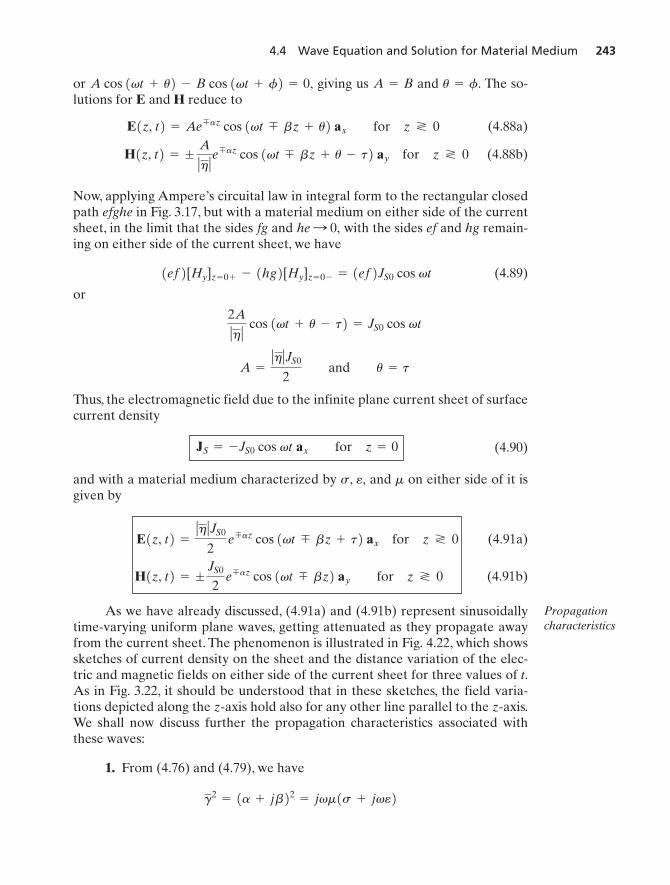
E = Ex1z, t2ax
JS = -JS0 cos vt ax
z = 0
� � H = J +0D0t
= Jc +0D0t
= sE + e 0E0t
� � E = - 0B0t
= -m 0H0t
H =Bm
D = eE Jc = sE
4.4 Wave Equation and Solution for Material Medium 239
z
y
x
JS
s, e, m s, e, m
FIGURE 4.21
Infinite plane current sheet embedded in a materialmedium.
RaoCh04v3.qxd 12/18/03 3:49 PM Page 239
240 Chapter 4 Fields and Waves In Material Media
The corresponding simplified forms of the Maxwell’s curl equations are
(4.72a)
(4.72b)
Without the term on the right side of (4.72b), these two equations would bethe same as (3.72a) and (3.72b) with replaced by and replaced by Theaddition of the term complicates the solution in time domain. Hence, it isconvenient to consider the solution for the sinusoidally time-varying case byusing the phasor technique. See Appendix A for phasor technique.
Thus, letting
(4.73a)
(4.73b)
and replacing and in (4.72a) and (4.72b) by their phasors and re-spectively, and by we obtain the corresponding differential equationsfor the phasors and as
(4.74a)
(4.74b)
Differentiating (4.74a) with respect to z and using (4.74b), we obtain
(4.75)
Defining
(4.76)
and substituting in (4.75), we have
(4.77)
which is the wave equation for in the material medium.The solution to the wave equation (4.77) is given by
(4.78)E –
x1z2 = A –
e-gqz + B –
egqz
E –
x
02E –
x
0z2 = g2E –
x
g = 1jvm1s + jve2
02E –
x
0z2 = -jvm
0H –
y
0z= jvm1s + jve2E –x
0H –
y
0z= -sE
–x - jveE
–x = -1s + jve2E –x
0E –
x
0z= -jvmH
–y
H –
yE –
x
jv,0>0tH –
y,E –
xHyEx
Hy1z, t2 = Re[H –
y1z2ejvt]
Ex1z, t2 = Re[E –
x1z2ejvt]
sEx
e.e0mm0
sEx
0Hy
0z= -sEx - e
0Ex
0t
0Ex
0z= -m
0Hy
0t
Waveequation
RaoCh04v3.qxd 12/18/03 3:49 PM Page 240
4.4 Wave Equation and Solution for Material Medium 241
where and are arbitrary constants. Noting that is a complex number and,hence, can be written as
(4.79)
and also writing and in exponential form as and respectively, wehave
or
(4.80)
We now recognize the two terms on the right side of (4.80) as representing uni-form plane waves propagating in the positive z- and negative z-directions, re-spectively, with phase constant in view of the factors and
respectively. They are, however, multiplied by the factorsand respectively. Hence, the amplitude of the field differs from one
constant phase surface to another. Since there cannot be a wave in the re-gion that is, to the left of the current sheet, and since there cannot be a
wave in the region that is, to the right of the current sheet, the solu-tion for the electric field is given by
(4.81)
To discuss how the amplitude of varies with z on either side of the cur-rent sheet, we note that since and are all positive, the phase angle of
lies between 90° and 180°, and hence the phase angle of liesbetween 45° and 90°, making and positive quantities. This means that decreases with increasing value of z, that is, in the positive z-direction, and decreases with decreasing value of z, that is, in the negative z-direction. Thus,the exponential factors and associated with the solutions for in(4.81) have the effect of decreasing the amplitude of the field, that is, attenu-ating it as it propagates away from the sheet to either side of it. For this rea-son, the quantity is known as the attenuation constant. The attenuation perunit length is equal to In terms of decibels, this is equal to or
The units of are nepers per meter. The quantity is known as thepropagation constant, since its real and imaginary parts, and together de-termine the propagation characteristics, that is, attenuation and phase shift ofthe wave.
Having found the solution for the electric field of the wave and dis-cussed its general properties, we now turn to the solution for the corresponding
b,a
ga8.686a dB.20 log10 e
a,ea.a
Exeaze-az
eaze-azba
gjvm1s + jve2 ms, e,Ex
E1z, t2 = eAe-az cos 1vt - bz + u2 ax for z 7 0Beaz cos 1vt + bz + f2 ax for z 6 0
z 7 0,1-2 z 6 0,1+2eaz,e-az
cos 1vt + bz + f2, cos 1vt - bz + u2b,
= Ae-az cos 1vt - bz + u2 + Beaz cos 1vt + bz + f2 = Re[Aejue-aze-jbzejvt + Bejfeazejbzejvt]
Ex1z, t2 = Re[E –
x1z2ejvt]
E –
x1z2 = Aejue-aze-jbz + Bejfeazejbz
Bejf,AejuB –
A –
g = a + jb
gB –
A –
Attenuationconstant
RaoCh04v3.qxd 12/18/03 3:49 PM Page 241
242 Chapter 4 Fields and Waves In Material Media
magnetic field by substituting for in (4.74a). Thus,
(4.82)
where
(4.83)
is the intrinsic impedance of the medium, which is now complex. Writing
(4.84)
we obtain the solution for as
(4.85)
Remembering that the first and second terms on the right side of (4.85) corre-spond to and waves, respectively, and, hence, represent the solutionsfor the magnetic field in the regions and respectively, we write
(4.86a)
(4.86b)
To complete the solution for the electromagnetic field due to the currentsheet embedded in the material medium, we need to find the values of the con-stants A, B, and To do this, we proceed in the same manner as in Sec. 3.4,using Fig. 3.17, except with a material medium on either side of the currentsheet. Thus, applying Faraday’s law in integral form to the rectangular closedpath abcda in the limit that the sides bc and with the sides ab and dc re-maining on either side of the current sheet, we have
(4.87)1ab2[Ex]z = 0 + - 1dc2[Ex]z = 0 - = 0
da : 0,
f.u,
H1z, t2 = d A
ƒh ƒ e-az cos 1vt - bz + u - t2 ay for z 7 0
- B
ƒh ƒ eaz cos 1vt + bz + f - t2 ay for z 6 0
z 6 0,z 7 01-21+2
=A
ƒh ƒ e-az cos 1vt - bz + u - t2 -
B
ƒh ƒ eaz cos 1vt + bz + f - t2
= Re c 1
ƒh ƒejt Aejue-aze-jbzejvt -1
ƒh ƒejt Bejfeazejbzejvt d Hy1z, t2 = Re[H
–y1z2ejvt]
Hy1z, t2h = ƒh ƒ ejt
h = A jvm
s + jve
=1h
1A –e-gq
z - B –
egqz2 = As + jve
jvm 1A –e-g
qz - B
–egqz2
H –
y = - 1
jvm
0E –
x
0z=g
jvm 1A –e-g
qz - B
–egqz2
E –
x
Electro-magnetic fielddue to thecurrent sheet
RaoCh04v3.qxd 12/18/03 3:49 PM Page 242
4.4 Wave Equation and Solution for Material Medium 243
or giving us and The so-lutions for E and H reduce to
(4.88a)
(4.88b)
Now, applying Ampere’s circuital law in integral form to the rectangular closedpath efghe in Fig. 3.17, but with a material medium on either side of the currentsheet, in the limit that the sides fg and with the sides ef and hg remain-ing on either side of the current sheet, we have
(4.89)
or
Thus, the electromagnetic field due to the infinite plane current sheet of surfacecurrent density
(4.90)
and with a material medium characterized by and on either side of it isgiven by
(4.91a)
(4.91b)
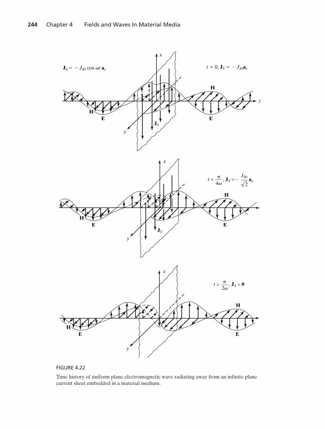
As we have already discussed, (4.91a) and (4.91b) represent sinusoidallytime-varying uniform plane waves, getting attenuated as they propagate awayfrom the current sheet. The phenomenon is illustrated in Fig. 4.22, which showssketches of current density on the sheet and the distance variation of the elec-tric and magnetic fields on either side of the current sheet for three values of t.As in Fig. 3.22, it should be understood that in these sketches, the field varia-tions depicted along the z-axis hold also for any other line parallel to the z-axis.We shall now discuss further the propagation characteristics associated withthese waves:
Time history of uniform plane electromagnetic wave radiating away from an infinite planecurrent sheet embedded in a material medium.
RaoCh04v3.qxd 12/18/03 3:49 PM Page 244
4.4 Wave Equation and Solution for Material Medium 245
or
(4.92a)(4.92b)
Squaring (4.92a) and (4.92b) and adding and then taking the square root, weobtain
(4.93)
From (4.92a) and (4.93), we then have
Since and are both positive, we finally get
(4.94)
(4.95)
We note from (4.94) and (4.95) that and are both dependent on throughthe factor This factor, known as the loss tangent, is the ratio of the magni-tude of the conduction current density to the magnitude of the displace-ment current density in the material medium. In practice, the loss tangentis, however, not simply inversely proportional to since both and are gen-erally functions of frequency. In fact, for many materials, the dependence of
on is more toward constant over wide frequency ranges.2. The phase velocity of the wave along the direction of propagation is
given by
(4.96)
We note that the phase velocity is dependent on the frequency of the wave. Thus,waves of different frequencies travel with different phase velocities. Consequent-ly, for a signal comprising a band of frequencies, the different frequency compo-nents do not maintain the same phase relationships as they propagate in themedium. This phenomenon is known as dispersion. We shall discuss dispersion indetail in Chapter 8.
vp =v
b=121me cB1 + a s
veb2
+ 1 d-1>2
vs>veesv,
jveE –
x
sE –
x
s>ve. sba
b =v1me12
cB1 + a sveb2
+ 1 d1>2 a =
v1me12 cB1 + a s
veb2
- 1 d1>2ba
b2 =12
cv2me + v2meB1 + a sveb2 d
a2 =12
c -v2me + v2meB1 + a sveb2 d
a2 + b2 = v2meB1 + a sveb2
2ab = vms a2 - b2 = -v2me
RaoCh04v3.qxd 12/18/03 3:49 PM Page 245
246 Chapter 4 Fields and Waves In Material Media
3. The wavelength in the medium is given by
(4.97)
In view of the attenuation of the wave with distance, the field variation with dis-tance is not sinusoidal. Hence, the wavelength is not exactly equal to the dis-tance between two consecutive positive maxima as in Fig. 3.23. It is, however,still exactly equal to the distance between two alternate zero crossings.
4. The ratio of the amplitude of the electric field to the amplitude of themagnetic field is equal to the magnitude of the complex intrinsic impedanceof the medium. The electric and magnetic fields are out of phase by the phaseangle of the intrinsic impedance. In terms of the phasor or complex field com-ponents, we have
(4.98)
5. From (4.76) and (4.83), we note that
(4.99a)
(4.99b)
so that
(4.100a)
(4.100b)
(4.100c)
Using (4.100a)–(4.100c), we can compute the material parameters and from a knowledge of the propagation parameters and at the frequency ofinterest.
6. To obtain the electromagnetic field due to a nonsinusoidal source, it isnecessary to consider its frequency components and apply superposition, sincewaves of different frequencies are attenuated by different amounts and travelwith different phase velocities. The nonsinusoidal signal changes shape as itpropagates in the material medium, unlike in the case of free space.
We shall now consider an example of the computation of and givenand f.s, e, m,
hg
hg
ms, e,
m =1
jv g h
e =1v
Imaghb
s = Reaghb
g
h= s + jve
g h = jvm
E –
x
H –
y= eh for the 1+2 wave
-h for the 1-2 wave
t,ƒh ƒ ,
l =2pb
=12
f1me cB1 + a sveb2
+ 1 d-1>2
RaoCh04v3.qxd 12/18/03 3:49 PM Page 246
4.4 Wave Equation and Solution for Material Medium 247
Example 4.5 Finding propagation parameters of a material mediumfrom its material parameters
The material parameters of a certain food item are given by andat the operating frequency of a microwave oven. We wish to find
the propagation parameters and Although explicit expressions for and in terms of and are given by
(4.94) and (4.95), it is instructive to compute their values by using complex algrebra inconjunction with the expression for given by (4.76). Thus, we have
so that
Proceeding in a similar manner with (4.83), we obtain
= 53.51l9.37°Æ
=54.9898
1.0276l -9.3685°
=120p147
111 - j0.3392
=h01er
111 - j1s>ve2
= A jvm
jve[1 - j1s>ve2]
h = A jvm
s + jve
vp =v
b= 0.4316 * 108 m>s
l =2pb
= 0.0176 m
b = 356.67 rad>m a = 58.85 Np>m
= 58.85 + j356.67
= 361.4912l80.6315°
= 351.782l90° * 1.0276l -9.3685°
= j351.78211.0560l -18.7369°
= j351.78211 - j0.3392
= j 2p * 2.45 * 109 * 147
3 * 108 A1 - j 2.17 * 36p
2p * 2.45 * 109 * 47 * 10-9
= j
v1er
c A1 - j s
vere0
= Bjvm – jvea1 - j s
veb
g = 1jvm1s + jve2g
mv, s, e,ba
h.a, b, l, vp,f = 2.45 GHzm = m0
s = 2.17 S>m, e = 47e0,
RaoCh04v3.qxd 12/18/03 3:49 PM Page 247
248 Chapter 4 Fields and Waves In Material Media
We shall conclude this section by generalizing the Poynting’s theorem(3.118), derived in Sec. 3.7, to a material medium.Thus, substituting so that and replacing by and by in (3.118), weobtain
(4.101)
where P is the instantaneous Poynting vector given by
(4.102)
We also recall that the time-average Poynting vector, is given by
(4.103)
In (4.101), the quantity is the power density associated with the work doneby the field, having to do with the conduction current in the material. Sincepower is dissipated in causing the conduction current to flow, it is the power dis-sipation density. Thus, it follows that the power dissipation density, the electricstored energy density, and the magnetic stored energy density, associated withelectric and magnetic fields in a material medium are given, respectively, by
(4.104a)
(4.104b)
(4.104c)
Example 4.6 Power flow for a uniform plane wave in seawater
Let us consider the electric field of a uniform plane wave propagating in seawater( and ) in the positive z-direction and having the electric field
at We wish to find the instantaneous power flow per unit area normal to the z-di-rection as a function of z and the time-average power flow per unit area normal to the z-direction as a function of z.
From the expression for E, we note that the frequency of the wave is 25 kHz. Atthis frequency in seawater, the propagation parameters can be computed to be
and The expressions for the instantaneous electric andmagnetic fields are therefore given by
H = 4.502e-0.628z cos 15 * 104pt - 0.628z - p>42 ay A>m E = 1e-0.628z cos 15 * 104pt - 0.628z2 ax V>m
h = 0.222l45°.a = b L 0.628
z = 0.
E = 1 cos 5 * 104 pt ax V>mm = m0s = 4 S>m, e = 80e0,
wm =12
mH2
we =12
eE2
pd = sE2
sE2
8P9 =12
Re [E � H*]
8P9,P = E � H
CSP # dS = -LV
1sE22 dv -00tLV
a12
eE2b
dv -00tLV
a12
mH2b
dv
m,m0ee0E # J = E # sE = sE2,J = Jc = sE
Poynting’stheorem for amaterialmedium
RaoCh04v3.qxd 12/18/03 3:49 PM Page 248
4.4 Wave Equation and Solution for Material Medium 249
The instantaneous Poynting vector is then given by
Thus, the instantaneous power flow per unit area normal to the z-direction, which is sim-ply the z-component of the instantaneous Poynting vector, is
Finally, the time-average power flow per unit area normal to the z-direction is
K4.4. Material medium; Sinusoidal waves; Material parameters; Propagation parame-ters;Attenuation and phase constants; Complex propagation constant; Complexintrinsic impedance; Poynting’s theorem for material medium; Power dissipa-tion density; Electric stored energy density; Magnetic stored energy density.
D4.7. Compute the propagation constant and intrinsic impedance for the followingcases: (a) and and (b)
and Ans. (a) (b)
D4.8. For a uniform plane wave of frequency propagating in a nonmagneticmaterial medium, the propagation constant is known to be Find the following: (a) the distance in which the fields are attenuated
by (b) the distance in which the fields undergo a change of phase by 1 rad;(c) the distance that a constant phase of the wave travels in (d) the ratio ofthe amplitudes of the electric and magnetic fields; and (e) the phase differencebetween the electric and magnetic fields.Ans. (a) 20 m; (b) 10 m; (c) 62.83 m; (d) (e)
D4.9. The magnetic field associated with a uniform plane wave propagating in thein a nonmagnetic material medium is given by
Find the following: (a) the instantaneous power flow across a surface of areain the plane at (b) the time-average power flow across a sur-
face of area in the plane; and (c) the time-average power flow acrossa surface of area in the plane.Ans. (a) (b) (c) 6.94H0
2 W.51.28H02 W;102.57H0
2 W;z = 1 m1 m2
z = 01 m2t = 0;z = 01 m2
H = H0 e-z cos 16p * 107t - 13z2 ay A>m1m = m02+z-direction
= 4.502e-1.256z cos 15 * 104pt - 0.628z2 P = E � H
RaoCh04v3.qxd 12/18/03 3:49 PM Page 249
250 Chapter 4 Fields and Waves In Material Media
4.5 UNIFORM PLANE WAVES IN DIELECTRICS AND CONDUCTORS
In the preceding section, we discussed uniform plane electromagnetic wavepropagation in a material medium for the general case. In this section, we con-sider special cases as follows:
Case 1: Perfect dielectrics. Perfect dielectrics are characterized by Then
(4.105)
is purely imaginary, so that
(4.106a)(4.106b)
(4.106c)
(4.106d)
Further,
(4.107)
is purely real. Thus, the waves propagate without attenuation and with the elec-tric and magnetic fields in phase, as in free space but with replaced by and
replaced by In terms of the relative permittivity and the relative perme-ability of the perfect dielectric medium, the propagation parameters are
(4.108a)
(4.108b)
(4.108c)
(4.108d)
where the quantities with subscripts “0” refer to free space.
Case 2: Imperfect dielectrics. Imperfect dielectrics are characterized bybut Recalling that is the conduction current density and
is the displacement current density, we note that this condition is equiva-lent to stating that the magnitude of the conduction current density is smallcompared to the magnitude of the displacement current density. Using the bi-nomial expansion
11 + x2n = 1 + nx +n1n - 12
2! x2 + Á
veE –
x
sE –
xs>ve � 1.s Z 0,
h = h0Amr
er
l =l01mrer
vp =c1mrer
b = b01mrer
mr
erm.m0
ee0
h = A jvm
jve= Ame
l =2pb
=1
f1me vp =v
b=
11me b = v1me a = 0
g = 1jvm –jve = jv1me s = 0.
RaoCh04v3.qxd 12/18/03 3:49 PM Page 250
4.5 Uniform Plane Waves in Dielectrics and Conductors 251
we can then write
(4.109)
so that
(4.110a)
(4.110b)
(4.110c)
(4.110d)
Further,
so that
(4.111)
In (4.109)–(4.111), we have retained all terms up to and including the secondpower in and have neglected all higher-order terms, since Fora value of equal to 0.1, the quantities and are different from thosefor the corresponding perfect dielectric case by a factor of only 1/800, whereasthe intrinsic impedance has a real part differing from the intrinsic impedance ofthe perfect dielectric medium by a factor of 3/800 and an imaginary part, whichis 1/20 of the intrinsic impedance of the perfect dielectric medium. Thus, for allpractical purposes, the only significant feature different from the perfect dielec-tric case is the attenuation.
Case 3: Good conductors. Good conductors are characterized byjust the opposite of imperfect dielectrics.This condition is equivalents>ve � 1,
lb, vp,s>ve s>ve � 1.s>ve
h L Ame c a1 -38
s3
v2e2 b + j s
2ved
= A jvm
jve a1 - j
s
veb-1>2
h = A jvm
s + jve
l =2pb
L1
f1me a1 -s2
8v2e2 b
vp =v
bL
11me a1 -s2
8v2e2 b
b L v1me a1 +s2
8v2e2 b
a Ls
2Ame a1 -s2
8v2e2 b
Ls
2Ame a1 -s2
8v2e2 b + jv1me a1 +s2
8v2e2 b
= Bjvm # jvea1 - j s
veb = jv1me a1 - j
s
veb1>2
g = 1jvm1s + jve2
RaoCh04v3.qxd 12/18/03 3:49 PM Page 251
252 Chapter 4 Fields and Waves In Material Media
to stating that the magnitude of the conduction current density is large com-pared to the magnitude of the displacement current density. Then
(4.112)
so that
(4.113a)(4.113b)
(4.113c)
(4.113d)
Further,
or
(4.114)
We note that and are proportional to provided that and areconstants. This behavior is much different from the imperfect dielectric case.
To discuss the propagation characteristics of a wave inside a good conduc-tor, let us consider the case of copper. The constants for copper are
and Hence, the frequency at which is equal to forcopper is equal to or Thus, at frequencies of evenseveral gigahertz, copper behaves like an excellent conductor. To obtain an ideaof the attenuation of the wave inside the conductor, we note that the attenuationundergone in a distance of one wavelength is equal to or In terms ofdecibels, this is equal to In fact, the field is attenuated bya factor or 0.368, in a distance equal to This distance is known as the skindepth and is denoted by the symbol From (4.113a), we obtain
4.5 Uniform Plane Waves in Dielectrics and Conductors 253
Underwatercommunica-tion
2F. Sterzer et al., “RF Therapy for Malignancy,” IEEE Spectrum, December 1980, pp. 32–37.
The skin depth for copper is equal to
Thus, in copper, the fields are attenuated by a factor in a distance of 0.066mm even at the low frequency of 1 MHz, thereby resulting in the concentrationof the fields near to the skin of the conductor.This phenomenon is known as theskin effect. It also explains shielding by conductors.
To discuss further the characteristics of wave propagation in a good con-ductor, we note that the ratio of the wavelength in the conducting medium tothe wavelength in a dielectric medium having the same and as those of theconductor is given by
(4.116)
Since For example, for seawater,and so that the ratio of the two wavelengths for
is equal to 0.00745. Thus, for the wavelength inseawater is 1/134 of the wavelength in a dielectric having the same and asthose of seawater and a still smaller fraction of the wavelength in free space.Furthermore, the lower the frequency, the smaller is this fraction. Since it is theelectrical length (i.e., the length in terms of the wavelength) instead of the physi-cal length that determines the radiation characteristics of an antenna, this meansthat antennas of much shorter length can be used in seawater than in free space.Together with the property that this illustrates that the lower the fre-quency, the more suitable it is for underwater communication.
For a given frequency, the higher the value of the greater is the value ofthe attenuation constant, the smaller is the value of the skin depth, and hence theless deep the waves can penetrate. For example, in the heating of malignant tis-sues (hyperthermia) by RF (radio-frequency) radiation, the waves penetratemuch deeper into fat (low water content) than into muscle (high water content).2
Equation (4.114) tells us that the intrinsic impedance of a good conductorhas a phase angle of 45°. Hence, the electric and magnetic fields in the mediumare out of phase by 45°. The magnitude of the intrinsic impedance is given by
(4.117)
As a numerical example, for copper, this quantity is equal toB2pf * 4p * 10-7
Thus, the intrinsic impedance of copper has as low a magnitude as evenat a frequency of In fact, by recognizing that
(4.118)
we note that the magnitude of the intrinsic impedance of a good conductormedium is a small fraction of the intrinsic impedance of a dielectric mediumhaving the same and It follows that for the same electric field, the magneticfield inside a good conductor is much larger than the magnetic field inside a di-electric having the same and as those of the conductor.
Case 4: Perfect conductors. Perfect conductors are idealizations of goodconductors in the limit that From (4.115), we note that the skin depth isequal to zero, and, hence, there is no penetration of fields into the material.Thus, no time-varying fields can exist inside a perfect conductor.
Summarizing the discussion of the special cases, we observe that as varies from 0 to a material is classified as a perfect dielectric for animperfect dielectric for but a good conductor for and fi-nally a perfect conductor in the limit that This implies that a material ofnonzero behaves as an imperfect dielectric for but as a good conduc-tor for where the transition frequency, is equal to In practice,however, the situation is not so simple because, as was already mentioned inSection 4.4, and are in general functions of frequency.
D4.10. For a nonmagnetic perfect dielectric material, find the relative per-mittivity for each of the following cases: (a) the phase velocity in the dielectric isone-third of its value in free space; (b) the rate of change of phase with distanceat a fixed time in the dielectric for a wave of frequency is the same as the rateof change of phase with distance at a fixed time in free space for a wave of fre-quency (c) for the same frequency, the wavelength in the dielectric is two-thirds of its value in free space; and (d) for the same electric-field amplitude, themagnetic-field amplitude in the dielectric is four times its value in free space.Ans. (a) 9; (b) 4; (c) 2.25; (d) 16.
D4.11. For a uniform plane wave of frequency propagating in a good con-ductor medium, the fields undergo attenuation by the factor in a distance of2.5 m. Find the following: (a) the distance in which the fields undergo a changeof phase by rad for (b) the distance by which a constant phasetravels in for and (c) the distance by which a constant phasetravels in for assuming the material parameters to be the sameas at Ans. (a) 5 m; (b) 0.5 m; (c) 0.1581 m.
D4.12. The electric fields of uniform plane waves of the same frequency propagating inthree different materials 1, 2, and 3 are given, respectively, by
(a) E1 = E0 e-0.4pz cos 12p * 105t - 0.4pz2 ax
f = 105 Hz.f = 104 Hz,1 msf = 105 Hz;1 ms
f = 105 Hz;2p
e-pf = 105 Hz
2f0;
f0
1m = m02
es
s>2pe.fq,f � fq,f � fqs
s: q .s � ve,� ve,s Z 0
s = 0,q ,s
s: q .
me
m.e
ƒh ƒ = A2pfms
= Aves Ame1012 Hz.0.369 Æ
RaoCh04v3.qxd 12/18/03 3:49 PM Page 254
4.6 Boundary Conditions 255
(b)(c)
For each material, determine if at the frequency of operation, it can be classifiedas an imperfect dielectric or a good conductor or neither of the two.Ans. (a) Good conductor; (b) Imperfect dielectric; (c) Neither.
4.6 BOUNDARY CONDITIONS
In our study of electromagnetics, we will be considering many problems involv-ing more than one medium. Examples are reflections of waves at an air–dielec-tric interface, determination of capacitance for a multiple-dielectric capacitor,and guiding of waves in a metallic waveguide. To solve a problem involving aboundary surface between different media, we need to know the conditions sat-isfied by the field components at the boundary.These are known as the boundaryconditions. They are a set of relationships relating the field components at apoint adjacent to and on one side of the boundary, to the field components at acorresponding point adjacent to and on the other side of the boundary.These re-lationships arise from the fact that Maxwell’s equations in integral form involveclosed paths and surfaces and they must be satisfied for all possible closed pathsand surfaces, whether they lie entirely in one medium or encompass a portion ofthe boundary between two different media. In the latter case, Maxwell’s equa-tions in integral form must be satisfied collectively by the fields on either side ofthe boundary, thereby resulting in the boundary conditions.
We shall derive the boundary conditions by considering the Maxwell’sequations
(4.119a)
(4.119b)
(4.119c)
(4.119d)
and applying them one at a time to a closed path or a closed surface encom-passing the boundary, and in the limit that the area enclosed by the closed pathor the volume bounded by the closed surface goes to zero. Thus, let us considertwo semi-infinite media separated by a plane boundary, as shown in Fig. 4.23.Let us denote the quantities pertinent to medium 1 by subscript 1 and the quan-tities pertinent to medium 2 by subscript 2. Let be the unit normal vector tothe surface and directed into medium 1, as shown in Fig. 4.23, and let all normalcomponents of fields at the boundary in both media denoted by an additionalsubscript n be directed along Let the surface charge density and the1C>m22an.
For deriving the boundaryconditions resulting from Faraday’slaw and Ampère’s circuital law.
surface current density (A/m) on the boundary be and respectively. Notethat, in general, the fields at the boundary in both media and the surface chargeand current densities are functions of position on the boundary.
First, we consider a rectangular closed path abcda of infinitesimal area inthe plane normal to the boundary and with its sides ab and cd parallel to and oneither side of the boundary, as shown in Fig. 4.23. Applying Faraday’s law(4.119a) to this path in the limit that ad and by making the area abcd tendto zero, but with ab and cd remaining on either side of the boundary, we have
(4.120)
In this limit, the contributions from ad and bc to the integral on the left side of(4.120) approach zero. Since ab and cd are infinitesimal, the sum of the contri-butions from ab and cd becomes where and arethe components of and along ab and cd, respectively. The right side of(4.120) is equal to zero, since the magnetic flux crossing the area abcd ap-proaches zero as the area abcd tends to zero. Thus, (4.120) gives
or, since ab and cd are equal and
(4.121)
Let us now define to be the unit vector normal to the area abcd and in the di-rection of advance of a right-hand screw as it is turned in the sense of the closedpath abcda. Noting then that is the unit vector along ab, we can write(4.121) as
Rearranging the order of the scalar triple product, we obtain
(4.122)as# an � 1E1 - E22 = 0
as � an# 1E1 - E22 = 0
as � an
as
Eab - Edc = 0
Edc = -Ecd,
Eab1ab2 + Ecd1cd2 = 0
E2E1
EcdEab[Eab1ab2 + Ecd1cd2],
limad : 0bc : 0Cabcda
E # dl = - limad : 0bc : 0
d
dt 3area
abcd
B # dS
bc : 0
JS,rS
Boundarycondition forEtangential
RaoCh04v3.qxd 12/18/03 3:49 PM Page 256
4.6 Boundary Conditions 257
Since we can choose the rectangle abcd to be in any plane normal to the bound-ary, (4.122) must be true for all orientations of It then follows that
(4.123a)
or, in scalar form,
(4.123b)
where and are the components of and respectively, tangential tothe boundary. In words, (4.123a) and (4.123b) state that at any point on theboundary, the components of and tangential to the boundary are equal.
Similarly, applying Ampère’s circuital law (4.119b) to the closed path inthe limit that ad and we have
(4.124)
Using the same argument as for the left side of (4.120), we obtain the quantityon the left side of (4.124) to be equal to where and
are the components of and along ab and cd, respectively. The secondintegral on the right side of (4.124) is zero since the displacement flux crossingthe area abcd approaches zero as the area abcd tends to zero. The first integralon the right side of (4.124) would also be equal to zero but for a contributionfrom the surface current on the boundary, because letting the area abcd tend tozero with ab and cd on either side of the boundary reduces only the volume cur-rent, if any, enclosed by it to zero, keeping the surface current still enclosed by it.This contribution is the surface current flowing normal to the line that abcd ap-proaches as it tends to zero, that is, Thus, (4.124) gives
or, since ab and cd are equal and
(4.125)
In terms of and we have
or
(4.126)
Since (4.126) must be true for all orientations of that is, for a rectangle abcdin any plane normal to the boundary, it follows that
(4.127a)an � 1H1 - H22 = JS
as,
as# an � 1H1 - H22 = as
# JS
as � an# 1H1 - H22 = JS
# as
H2,H1
Hab - Hdc = JS# as
Hdc = -Hcd,
Hab1ab2 + Hcd1cd2 = 1JS# as21ab2
[JS# as]1ab2.
H2H1Hcd
Hab[Hab1ab2 + Hcd1cd2],
limad : 0bc : 0Cabcda
H # dl = limad : 0bc : 0 3area
abcd
J # dS + limad : 0bc : 0
d
dt 3area
abcd
D # dS
bc : 0,
E2E1
E2,E1Et2Et1
Et1 - Et2 = 0
an � 1E1 - E22 = 0
as.
Boundarycondition forHtangential
RaoCh04v3.qxd 12/18/03 3:49 PM Page 257
258 Chapter 4 Fields and Waves In Material Media
or, in scalar form,
(4.127b)
where and are the components of and respectively, tangential tothe boundary. In words, (4.127a) and (4.127b) state that at any point on theboundary, the components of and tangential to the boundary are discon-tinuous by the amount equal to the surface current density at that point. It shouldbe noted that the information concerning the direction of relative to that of
which is contained in (4.127a), is not present in (4.127b). Thus, ingeneral, (4.127b) is not sufficient, and it is necessary to use (4.127a).
Now, we consider a rectangular box abcdefgh of infinitesimal volume en-closing an infinitesimal area of the boundary and parallel to it, as shown inFig. 4.24. Applying Gauss’ law for the electric field (4.119c) to this box in thelimit that the side surfaces (abbreviated ss) tend to zero by making the vol-ume of the box tend to zero but with the sides abcd and efgh remaining on ei-ther side of the boundary, we have
(4.128)
In this limit, the contributions from the side surfaces to the integral on the leftside of (4.128) approach zero. The sum of the contributions from the top andbottom surfaces becomes since abcd and efgh are in-finitesimal. The quantity on the right side of (4.128) would be zero but for thesurface charge on the boundary, since letting the volume of the box tend to zerowith the sides abcd and efgh on either side of it reduces only the volume charge,if any, enclosed by it to zero, keeping the surface charge still enclosed by it. Thissurface charge is equal to Thus, (4.128) gives
or, since abcd and efgh are equal,
(4.129a)Dn1 - Dn2 = rS
Dn11abcd2 - Dn21efgh2 = rS1abcd2rS1abcd2.
[Dn11abcd2 - Dn21efgh2]
limss:0 C
surfaceof the box
D # dS = limss:0 3
volumeof the box
r dv
1H1 - H22,JS
H2H1
H2,H1Ht2Ht1
Ht1 - Ht2 = JS
Boundarycondition forDnormal
a
d c
gb
an
Medium 1
Medium 2
h
e fFIGURE 4.24
For deriving the boundaryconditions resulting from thetwo Gauss’ laws.
RaoCh04v3.qxd 12/18/03 3:49 PM Page 258
4.6 Boundary Conditions 259
In terms of and (4.129a) is given by
(4.129b)
In words, (4.129a) and (4.129b) state that at any point on the boundary, the com-ponents of and normal to the boundary are discontinuous by the amountof the surface charge density at that point.
Similarly, applying Gauss’ law for the magnetic field (4.119d) to the boxabcdefgh in the limit that the side surfaces tend to zero, we have
(4.130)
Using the same argument as for the left side of (4.128), we obtain the quantity onthe left side of (4.130) to be equal to Thus, (4.130) gives
or, since abcd and efgh are equal
(4.131a)
In terms of and (4.131a) is given by
(4.131b)
In words, (4.131a) and (4.131b) state that at any point on the boundary, the com-ponents of and normal to the boundary are equal.
Summarizing the boundary conditions, we have
(4.132a)
(4.132b)
(4.132c)
(4.132d)
or, in scalar form,
(4.133a)
(4.133b)
(4.133c)
(4.133d)
as illustrated in Fig. 4.25. Although we have derived these boundary conditionsby considering a plane interface between the two media, it should be obviousthat we can consider any arbitrary-shaped boundary and obtain the same resultsby letting the sides ab and cd of the rectangle and the top and bottom surfaces of
Bn1 - Bn2 = 0
Dn1 - Dn2 = rS
Ht1 - Ht2 = JS
Et1 - Et2 = 0
an# 1B1 - B22 = 0
an# 1D1 - D22 = rS
an � 1H1 - H22 = JS
an � 1E1 - E22 = 0
B2B1
an# 1B1 - B22 = 0
B2,B1
Bn1 - Bn2 = 0
Bn11abcd2 - Bn21efgh2 = 0
[Bn11abcd2 - Bn21efgh2].
limss:0 C
surfaceof the box
B # dS = 0
D2D1
an# 1D1 - D22 = rS
D2,D1
Boundarycondition forBnormal
RaoCh04v3.qxd 12/18/03 3:49 PM Page 259
260 Chapter 4 Fields and Waves In Material Media
anMedium 1
Medium 2
�Et1
Et2
Ht1
Dn1
Bn1
Bn2Dn2
Ht2
rSJS
FIGURE 4.25
For illustrating the boundary conditions at an interface between two different media.
the box tend to zero, in addition to the limits that the sides ad and bc of the rec-tangle and the side surfaces of the box tend to zero.
The boundary conditions given by (4.132a) – (4.132d) are general. Whenthey are applied to particular cases, the special properties of the pertinentmedia come into play. Two such cases are important to be considered. They areas follows.
Interface between two perfect dielectric media: Since for a perfect di-electric, Thus, there cannot be any conduction current in aperfect dielectric, which in turn rules out any accumulation of free charge on thesurface of a perfect dielectric. Hence, in applying the boundary conditions(4.132a)–(4.132d) to an interface between two perfect dielectric media, we set
and equal to zero, thereby obtaining
(4.134a)(4.134b)(4.134c)(4.134d)
These boundary conditions tell us that the tangential components of E and Hand the normal components of D and B are continuous at the boundary.
Surface of a perfect conductor: No time-varying fields can exist in a per-fect conductor. In view of this, the boundary conditions on a perfect conductorsurface are obtained by setting the fields with subscript 2 in (4.132a) – (4.132d)equal to zero. Thus, we obtain
(4.135a)(4.135b)(4.135c)(4.135d) an
# B = 0 an
# D = rS
an � H = JS
an � E = 0
an# 1B1 - B22 = 0
an# 1D1 - D22 = 0
an � 1H1 - H22 = 0 an � 1E1 - E22 = 0
JSrS
s = 0, Jc = sE = 0.
Boundaryconditions ona perfectconductorsurface
RaoCh04v3.qxd 12/18/03 3:49 PM Page 260
4.6 Boundary Conditions 261
where we have also omitted subscripts 1, so that E, H, D, and B are the fields onthe perfect conductor surface. The boundary conditions (4.135a) and (4.135d)tell us that on a perfect conductor surface, the tangential component of the elec-tric field intensity and the normal component of the magnetic field intensity arezero. Hence, the electric field must be completely normal, and the magneticfield must be completely tangential to the surface. The remaining two boundaryconditions (4.135c) and (4.135b) tell us that the (normal) displacement flux den-sity is equal to the surface charge density and the (tangential) magnetic field in-tensity is equal in magnitude to the surface current density.
Example 4.7 Application of boundary conditions
In Fig. 4.26, the region is a perfect conductor, the region is a perfect di-electric of and and the region is free space. The electric and mag-netic fields in the region are given at a particular instant of time by
We wish to find (a) and on the surface and (b) E and H for that is, im-mediately adjacent to the and on the free-space side, at that instant of time.
(a) Denoting the perfect dielectric medium to be medium 1 and the per-fect conductor medium to be medium 2, we have and all fieldswith subscript 2 are equal to zero. Then from (4.132c) and (4.132b), we obtain
Note that the remaining two boundary conditions (4.132a) and (4.132d) are al-ready satisfied by the given fields, since and do not exist and for
Also note that what we have done here is equivalent to using (4.135a) –(4.135d), since the boundary is the surface of a perfect conductor.Ez = 0.
x = 0,BxEy
= H1 sin 2pz az
[JS]x = 0 = an � [H1]x = 0 = ax � H1 sin 2pz ay
= 2e0 E1 sin 2pz
[rS]x = 0 = an# [D1]x = 0 = ax
# 2e0 E1 sin 2pz ax
an = ax,1x 6 0210 6 x 6 d2
x = d planex = d+ ,x = 0JSrS
H = H1 cos px sin 2pz ay
E = E1 cos px sin 2pz ax + E2 sin px cos 2pz az
0 6 x 6 dx 7 dm = m0,e = 2e0
0 6 x 6 dx 6 0
zy
x � d
x � 0
x
Free Spacee0, m0
Perfect Dielectric2e0, m0
Perfect Conductor
FIGURE 4.26
For illustrating the application of boundary conditions.
RaoCh04v3.qxd 12/18/03 3:49 PM Page 261
262 Chapter 4 Fields and Waves In Material Media
(b) Denoting the perfect dielectric medium to be medium 1 and thefree-space medium to be medium 2 and setting we obtain from(4.133a) and (4.133c)
Thus
Setting and using (4.133b) and (4.133d), we obtain
Thus,
Note that what we have done here is equivalent to using (4.134a) – (4.134d), sincethe boundary is the interface between two perfect dielectrics.
K4.6. Boundary conditions; Tangential component of E; Tangential component of H;Normal component of D; Normal component of B.
D4.13. For each of the following values of the displacement flux density at a point on thesurface of a perfect conductor (no electric field inside and hence on the sur-face), find the surface charge density at that point: (a)and pointing away from the surface; (b) and pointing towardthe surface; and (c) and pointing away from the surface.Assume to be positive for all cases.Ans. (a) (b) (c)
D4.14. The region is a perfect dielectric of permittivity and the region is a perfect dielectric of permittivity Consider the field components at point1 on the of the boundary to be denoted by subscript 1 and the fieldcomponents at the adjacent point 2 on the of the boundary to be de-noted by subscript 2. If find the following: (a) (b)
and (c)Ans. (a) 1.5; (b) (c)
D4.15. The plane forms the boundary between free space and anothermedium. Find the following: (a) at if is a perfect conductorand (b) if is a magneticz 6 0H10, 0, 0+2H10, 0, 0+2 = H013ax - 4ay2 cos vt;
z 6 0t = 0JS10, 0, 021z 7 02z = 0
2>15.3>15;D1>D2.E1>E2;
Ex1>Ex2;E1 = E012ax + ay2,-x-side
+x-side3e0.
x 6 02e0x 7 0D0.-2D0;3D0;
D0
D = D010.8ax + 0.6ay2D = D01ax + 13az2
D = D01ax - 2ay + 2az2Et = 0
[H]x = d + = H1 cos pd sin 2pz ay
[Bx]x = d + = [Bx]x = d - = 0
[Hz]x = d + = [Hz]x = d - = 0
[Hy]x = d + = [Hy]x = d - = H1 cos pd sin 2pz
JS = 0
[E]x = d + = 2E1 cos pd sin 2pz ax + E2 sin pd cos 2pz az
= 2E1 cos pd sin 2pz
[Ex]x = d + =1e0
[Dx]x = d +
= 2e0 E1 cos pd sin 2pz
[Dx]x = d + = [Dx]x = d - = 2e0[Ex]x = d -
[Ez]x = d + = [Ez]x = d - = E2 sin pd cos 2pz
[Ey]x = d + = [Ey]x = d - = 0
rS = 0,1x 7 d210 6 x 6 d2
RaoCh04v3.qxd 12/18/03 3:49 PM Page 262
4.7 Reflection and Transmission of Uniform Plane Waves 263
material of and and (c) the ratio ofto for the case of (b).
Ans. (a) (b) (c) 8.989.
4.7 REFLECTION AND TRANSMISSION OF UNIFORM PLANE WAVES
Thus far, we have considered uniform plane wave propagation in unboundedmedia. Practical situations are characterized by propagation involving several dif-ferent media. When a wave is incident on a boundary between two differentmedia, a reflected wave is produced. In addition, if the second medium is not a per-fect conductor, a transmitted wave is set up. Together, these waves satisfy theboundary conditions at the interface between the two media. In this section, weshall consider these phenomena for waves incident normally on plane boundaries.
To do this, let us consider the situation shown in Fig. 4.27 in which steady-state conditions are established by uniform plane waves of radian frequency propagating normal to the plane interface between two media character-ized by two different sets of values of and where We shall as-sume that a wave is incident from medium onto the interface,thereby setting up a reflected wave in that medium, and a transmitted wave in medium For convenience, we shall work with the phasor orcomplex field components. Thus, considering the electric fields to be in the x-di-rection and the magnetic fields to be in the y-direction, we can write the solu-tion for the complex field components in medium 1 to be
(4.136a)
(4.136b)
where and are the incident and reflected wave electric andmagnetic field components, respectively, at in medium 1 and
(4.137a)
(4.137b) h1 = A jvm1
s1 + jve1
g1 = 1jvm11s1 + jve12z = 0-
H –
1-E
–1+, E
–1-, H
–1+,
=1h1
1E –1+e-g
q1 z - E –
1-egq1 z2
H –
1y1z2 = H –
1+e-g
q1 z + H –
1-egq1 z
E –
1x1z2 = E –
1+e-g
q1 z + E –
1-egq1 z
2 1z 7 02. 1+21-2 1 1z 6 021+2 s Z q .m,s, e,z = 0
Normal incidence of uniform planewaves on a plane interface betweentwo different media.
RaoCh04v3.qxd 12/18/03 3:49 PM Page 263
264 Chapter 4 Fields and Waves In Material Media
Recall that the real field corresponding to a complex field component is ob-tained by multiplying the complex field component by and taking the realpart of the product. The complex field components in medium 2 are given by
(4.138a)
(4.138b)
where and are the transmitted wave electric- and magnetic-field compo-nents at in medium 2 and
(4.139a)
(4.139b)
To satisfy the boundary conditions at we note that (1) the compo-nents of both electric and magnetic fields are entirely tangential to the interfaceand (2) in view of the finite conductivities of the media, no surface current existson the interface (currents flow in the volumes of the media). Hence, from thephasor forms of the boundary conditions (4.133a) and (4.133b), we have
(4.140a)
(4.140b)
Applying these to the solution pairs given by (4.136a, b) and (4.138a, b), we have
(4.141a)
(4.141b)
We now define the reflection coefficient at the boundary, denoted by the symbolto be the ratio of the reflected wave electric field at the boundary to the inci-
dent wave electric field at the boundary. From (4.141a) and (4.141b), we obtain
(4.142)
Note that the ratio of the reflected wave magnetic field at the boundary to theincident wave magnetic field at the boundary is given by
(4.143)
The ratio of the transmitted wave electric field at the boundary to the incidentwave electric field at the boundary, known as the transmission coefficient and
H –
1-
H –
1+ =
-E –
1->h1
E –
1+>h1
= -
E –
1-
E –
1+ = -≠
≠ =E –
1-
E –
1+ =
h2 - h1
h2 + h1
≠,
1h1
1E –1+ - E
–1-2 =
1h2
E –
2+
E –
1+ + E
–1- = E
–2+
[H –
1y]z = 0 = [H –
2y]z = 0
[E –
1x]z = 0 = [E –
2x]z = 0
z = 0,
h2 = A jvm2
s2 + jve2
g2 = 1jvm21s2 + jve22z = 0+
H –
2+E
–2+
=E –
2+
h2 e-qg2 z
H –
2y1z2 = H –
2+e-q
g2 z
E –
2x1z2 = E –
2+e-q
g2 z
ejvt
Reflectionandtransmissioncoefficients
RaoCh04v3.qxd 12/18/03 3:49 PM Page 264
4.7 Reflection and Transmission of Uniform Plane Waves 265
denoted by the symbol is given by
(4.144)
where we have used (4.141a). The ratio of the transmitted wave magnetic fieldat the boundary to the incident wave magnetic field at the boundary is given by
(4.145)
The reflection and transmission coefficients given by (4.142) and (4.144),respectively, enable us to find the reflected and transmitted wave fields for agiven incident wave field. We observe the following properties of and
1. For and The incident wave is entirely transmitted.The situation then corresponds to a “matched” condition.A trivial case oc-curs when the two media have identical values of the material parameters.
2. For that is, when both media are perfect dielectrics, andare real. Hence, and are real. In particular, if the two media have the
same permeability but different permittivities and then
(4.146)
(4.147)
3. For and Thus, if medium 2 is a perfectconductor, the incident wave is entirely reflected, as it should be since therecannot be any time-varying fields inside a perfect conductor.The superposi-tion of the reflected and incident waves would then give rise to the so-calledcomplete standing waves in medium 1. We shall discuss complete standingwaves as well as partial standing waves when we study the topic of sinu-soidal steady-state analysis of waves on transmission lines in Chapter 7.
Example 4.8 Normal incidence of a uniform plane wave onto a materialmedium
Region is free space, whereas region is a material medium charac-terized by and For a uniform plane wave having theelectric field
Ei = E0 cos 13p * 105t - 10-3pz2 ax V>m
m = m0.s = 10-4 S>m, e = 5e0,2 1z 7 021 1z 6 02
t: 0.s2 : q , h2 : 0, ≠ : -1,
t =2
1 + 1e2>e1
=1 - 1e2>e1
1 + 1e2>e1
≠ =1m>e2 - 1m>e11m>e2 + 1m>e1
e2,e1m
t≠h2
h1s1 = s2 = 0,
t = 1.h2 = h1, ≠ = 0
t:≠
H –
2+
H –
1+ =
H –
1+ + H
–1-
H –
1+ = 1 - ≠
t =E –
2+
E –
1+ =
E –
1+ + E
–1-
E –
1+ = 1 + ≠
t,
RaoCh04v3.qxd 12/18/03 3:49 PM Page 265
266 Chapter 4 Fields and Waves In Material Media
incident on the interface from region 1, we wish to obtain the expressions for thereflected and transmitted wave electric and magnetic fields.
From computation as in Example 4.5 for and
Then
Thus, the reflected and transmitted wave electric and magnetic fields are given by
Note that at the boundary conditions of and are sat-isfied, since
and
K4.7. Plane interface between two material media; Normal incidence of uniformplane waves; Reflection; Transmission; Reflection and transmission coefficients.
D4.16. For each of the following cases of uniform plane waves of frequency incident normally from medium onto the interface withmedium find the values of and (a) Medium 1 is free space andthe parameters of medium 2 are and and (b) them = m0;s = 10-3 S>m, e = 6e0,
t:≠2 1z 7 02,1z = 021 1z 6 02
f = 1 MHz
E0
377- 1.678 * 103E0 cos 0.8976p = 4.277 * 103E0 cos 1- 0.0396p2
E0 + 0.6325E0 cos 0.8976p = 0.4472E0 cos 0.1476p
Hi + Hr = HtEi + Er = Etz = 0,
– cos 13p * 105t - 9.425 * 10-3z - 0.0396p2 ay A>m = 4.277 * 10-3E0 e-
6.283 * 10-3z
– cos 13p * 105t - 9.425 * 10-3z + 0.1476p - 0.1872p2 ay A>m Ht =
0.4472E0
104.559 e-
6.283 * 10-3z
– cos 13p * 105t - 9.425 * 10-3z + 0.1476p2 ax V>m Et = 0.4472E0 e-
6.283 * 10-3z
= -1.678 * 10-3E0 cos 13p * 105t + 10-3pz + 0.8976p2 ay A>m Hr = -
0.6325E0
377 cos 13p * 105t + 10-3pz + 0.8976p2 ay A>m
Er = 0.6325E0 cos 13p * 105t + 10-3pz + 0.8976p2 ax V>m
= 0.4472l26.565° = 0.4472l0.1476p
t = 1 + ≠ = 1 + 0.6325l161.565°
= 0.6325l161.565° = 0.6325l0.8976p
≠ =h - h0
h + h0=
104.559l33.69° - 377
104.559l33.69° + 377
h = 104.559l33.69° = 104.559l0.1872p
g = 16.283 + j9.4252 * 10-3
f = 13p * 1052>2p = 1.5 * 105 Hz,s = 10-4 S>m, e = 5e0, m = m0,
z = 0
RaoCh04v3.qxd 12/18/03 3:49 PM Page 266
Summary 267
parameters of medium 1 are and and the parame-ters of medium 2 are and Ans. (a) (b)
D4.17. The regions and are nonmagnetic perfect dielectrics ofpermittivities and respectively. For a uniform plane wave incident from theregion normally onto the boundary find for each of the fol-lowing to hold at (a) the electric field of the reflected wave is timesthe electric field of the incident wave; (b) the electric field of the transmittedwave is 0.4 times the electric field of the incident wave; and (c) the electric fieldof the transmitted wave is six times the electric field of the reflected wave.Ans. (a) 4; (b) 16; (c) 4/9.
SUMMARY
In this Chapter, we introduced materials. We learned that materials can be clas-sified as (1) conductors, (2) semiconductors, (3) dielectrics, and (4) magneticmaterials, depending on the nature of the response of the charged particles inthe materials to applied fields. Conductors are characterized by conduction,which is the phenomenon of steady drift of free electrons under the influence ofan applied electric field, thereby resulting in a conduction current. In semicon-ductors, also characterized by conduction, the charge carriers are not only elec-trons, but also holes.We learned that the conduction current density is related tothe electric field intensity in the manner
(4.148)
where is the conductivity of the material. We discussed (1) the formation ofsurface charge at the boundaries of a conductor placed in a static electric field,(2) the derivation of Ohm’s law in circuit theory, and (3) the Hall effect.
Dielectrics are characterized by polarization, which is the phenomenonof the creation and net alignment of electric dipoles, formed by the displace-ment of the centroids of the electron clouds from the centroids of the nucleii ofthe atoms, along the direction of an applied electric field. Magnetic materialsare characterized by magnetization, which is the phenomenon of net alignmentof the axes of the magnetic dipoles, formed by the electron orbital and spin mo-tion around the nucleii of the atoms, along the direction of an applied magnet-ic field. To eliminate the need for explicitly taking into account the effects ofpolarization and magnetization, we revised the definitions of the displacementflux density vector and the magnetic field intensity vector, introduced in Sec.2.3 for free space, to be applicable for a material medium. The revised defini-tions are
H =Bm0
- M
D = e0 E + P
s
Jc = sE
-1>3z = 0:e2>e1z = 0,z 6 0
e2,e1
1m = m02z 7 0z 6 0
1.948l -1.177°.0.9486l-2.4155°,0.6909l64.177°, 0.3846l29.331°;m = m0.s = 10-3 S>m, e = 80e0,m = m0,s = 4 S>m, e = 80e0,
RaoCh04v3.qxd 12/18/03 3:49 PM Page 267
268 Chapter 4 Fields and Waves In Material Media
respectively, where P is the polarization vector, and M is the magnetization vec-tor. We learned that for isotropic materials, these expressions simplify to
(4.149)
(4.150)
where
are the permittivity and the permeability, respectively, of the material and thequantities and are the relative permittivity and the relative permeability,respectively, which take into account implicitly the effects of polarization andmagnetization, respectively. Equations (4.148), (4.149), and (4.150) are knownas the constitutive relations.We also discussed the hysteresis phenomenon asso-ciated with ferromagnetic materials and discussed an application based on theuse of the hysteresis curve.
Next, we extended the treatment of uniform plane waves to a materialmedium. Starting with Maxwell’s equations for a material medium given by
and using the phasor technique, we considered the infinite plane current sheetof uniform surface current density
in the xy-plane and embedded in the material medium, and obtained the elec-tromagnetic field due to it to be
(4.151a)
(4.151b)
In (4.151a, b), and are the attenuation and phase constants given, respec-tively, by the real and imaginary parts of the propagation constant, Thus,
The quantities and are the magnitude and phase angle, respectively, of theintrinsic impedance, of the medium. Thus,
h = ƒh ƒ ejt = A jvm
s + jve
h,tƒh ƒ
g = a + jb = 1jvm1s + jve2g.
ba
H = ;
JS0
2 e < az cos 1vt < bz2 ay for z � 0
E =ƒh ƒJS0
2 e < az cos 1vt < bz + t2 ax for z � 0
JS = -JS0 cos vt ax A>m
� � H = Jc +0D0t
= sE + e 0E0t
� � E = - 0B0t
= -m 0H0t
mrer
m = m0mr
e = e0er
H =Bm
D = eE
RaoCh04v3.qxd 12/18/03 3:49 PM Page 268
Summary 269
The solution given by (4.151a) and (4.151b) tells us that the wave propagationin the material medium is characterized by attenuation, as indicated by anda phase difference between E and H in the amount We also learned that theseproperties as well as the phase velocity are frequency-dependent.
We also generalized the Poynting’s theorem, introduced in Sec. 3.7 for freespace, to a material medium and learned that the power dissipation density as-sociated with the phenomenon of conduction, and the electric and magneticstored energy densities are given, respectively, by
The power flow out of a closed surface S, as given by the surface integral of thePoynting vector, P, over S, plus the power dissipated in the volume V boundedby S, is always equal to the sum of the time rates of decrease of the electric andmagnetic stored energies in the volume V, as given by the Poynting’s theorem
Having discussed uniform plane wave propagation for the general case ofa medium characterized by and we then considered several specialcases. These are summarized in the following:
Perfect dielectrics. For these materials, Wave propagation occurs with-out attenuation as in free space but with the propagation parameters governedby and instead of and respectively.
Imperfect dielectrics. A material is classified as an imperfect dielectric forthat is, conduction current density small in magnitude compared to
the displacement current density. The only significant feature of wave propaga-tion in an imperfect dielectric as compared to that in a perfect dielectric is theattenuation undergone by the wave.
Good conductors. A material is classified as a good conductor for that is, conduction current density large in magnitude compared to the displace-ment current density. Wave propagation in a good conductor medium is charac-terized by attenuation and phase constants both equal to Thus for largevalues of f and/or the fields do not penetrate very deep into the conductor.This phenomenon is known as the skin effect. From considerations of the fre-quency dependence of the attenuation and wavelength for a fixed we learnedthat low frequencies are more suitable for communication with underwater ob-jects. We also learned that the intrinsic impedance of a good conductor mediumis very low in magnitude compared to that of a dielectric medium having thesame and m.e
s,
s,1pfms.
s W ve,
s V ve,
m0,e0me
s = 0.
m,s, e,
CSP # dS = -LV
sE2 dv -00tLv
12
eE2 dv -00tLv
12
mH2 dv
wm = 12 mH2
we = 12 eE2
pd = sE2
t.e <az
RaoCh04v3.qxd 12/18/03 3:49 PM Page 269
270 Chapter 4 Fields and Waves In Material Media
Perfect conductors. These are idealizations of good conductors in the limitFor the skin depth, that is, the distance in which the fields in-
side a conductor are attenuated by a factor is zero. Hence, there can be nopenetration of fields into a perfect conductor.
As a prelude to the consideration of problems involving more than onemedium, we derived the boundary conditions resulting from the application ofMaxwell’s equations in integral form to closed paths and closed surfaces en-compassing the boundary between two media, and in the limits that the areasenclosed by the closed paths and the volumes bounded by the closed surfacesgo to zero. These boundary conditions are given by
where the subscripts 1 and 2 refer to media 1 and 2, respectively, and is unitvector normal to the boundary at the point under consideration and directedinto medium 1. In words, the boundary conditions state that at a point on theboundary, the tangential components of E and the normal components of B arecontinuous, whereas the tangential components of H are discontinuous by theamount equal to at that point, and the normal components of D are discon-tinuous by the amount equal to at that point.
Two important special cases of boundary conditions are as follows: (a) Atthe boundary between two perfect dielectrics, the tangential components of Eand H and the normal components of D and B are continuous. (b) On the sur-face of a perfect conductor, the tangential component of E and the normal com-ponent of B are zero, whereas the normal component of D is equal to thesurface charge density, and the tangential component of H is equal in magni-tude to the surface current density.
Finally, we considered uniform plane waves incident normally onto aplane boundary between two media, and we learned how to compute the re-flected and transmitted wave fields for a given incident wave field.
REVIEW QUESTIONS
Q4.1. Distinguish between bound electrons and free electrons in an atom and brieflydescribe the phenomenon of conduction.
Q4.2. Discuss the classification of a material as a conductor, semiconductor, or dielec-tric with the aid of energy band diagrams.
Q4.3. What is mobility? Give typical values of mobilities for electrons and holes.Q4.4. State Ohm’s law valid at a point, defining the conductivities for conductors and
semiconductors.Q4.5. Explain how conduction current in a material is taken into consideration in
Maxwell’s equations.Q4.6. Discuss the formation of surface charge at the boundaries of a conductor placed
in a static electric field.
rS
JS
an
an# 1B1 - B22 = 0
an# 1D1 - D22 = rS
an � 1H1 - H22 = JS
an � 1E1 - E22 = 0
e-1,s = q ,s: q .
RaoCh04v3.qxd 12/18/03 3:49 PM Page 270
Review Questions 271
Q4.7. Discuss the derivation of Ohm’s law in circuit theory from the Ohm’s law validat a point.
Q4.8. Discuss the Hall effect.
Q4.9. Briefly describe the phenomenon of polarization in a dielectric material. Whatare the different kinds of polarization?
Q4.10. What is an electric dipole? How is its strength defined?
Q4.11. What is a polarization vector? How is it related to the electric field intensity?
Q4.12. Discuss the effect of polarization in a dielectric material using the example ofpolarization surface charge.
Q4.13. Discuss how polarization current arises in a dielectric material. How is it takeninto account in Maxwell’s equations?
Q4.14. Discuss the revised definition of displacement flux density and the permittivityconcept.
Q4.15. What is an anisotropic dielectric material? When can an effective permittivitybe defined for an anisotropic dielectric material?
Q4.16. Briefly describe the phenomenon of magnetization in a magnetic material.What are the different kinds of magnetic materials?
Q4.17. What is a magnetic dipole? How is its strength defined?
Q4.18. What is a magnetization vector? How is it related to the magnetic flux density?
Q4.19. Discuss the effect of magnetization in a magnetic material using the example ofmagnetization surface current.
Q4.20. Discuss how magnetization current arises in a magnetic material. How is ittaken into account in Maxwell’s equations?
Q4.21. Discuss the revised definition of magnetic field intensity and the permeabilityconcept.
Q4.22. Discuss the phenomenon of hysteresis associated with ferromagnetic materials.
Q4.23. Discuss the principles behind storing data on a floppy disk and retrieving thedata from it.
Q4.24. State the constitutive relations for a material medium.
Q4.25. Discuss the determination of the electromagnetic field due to an infinite planecurrent sheet of sinusoidally time-varying current density embedded in a materialmedium, explaining how it is made convenient by using the phasor technique.
Q4.26. What is the propagation constant for a material medium? Discuss the signifi-cance of its real and imaginary parts.
Q4.27. What is the intrinsic impedance for a material medium? What is the conse-quence of its complex nature?
Q4.28. What is loss tangent? Discuss its significance.
Q4.29. Discuss the consequence of the frequency dependence of the phase velocity of awave in a material medium.
Q4.30. How would you obtain the electromagnetic field due to a current sheet of non-sinusoidally time-varying current density embedded in a material medium?
Q4.31. State Poynting’s theorem for a material medium.
Q4.32. What are the power dissipation density, the electric stored energy density, andthe magnetic stored energy density associated with an electromagnetic field in amaterial medium?
RaoCh04v3.qxd 12/18/03 3:49 PM Page 271
272 Chapter 4 Fields and Waves In Material Media
Q4.33. What is the condition for a medium to be a perfect dielectric? How do the char-acteristics of wave propagation in a perfect dielectric medium differ from thoseof wave propagation in free space?
Q4.34. What is the criterion for a material to be an imperfect dielectric? What is thesignificant feature of wave propagation in an imperfect dielectric as comparedto that in a perfect dielectric?
Q4.35. What is the criterion for a material to be a good conductor? Give two exam-ples of materials that behave as good conductors for frequencies of up to sev-eral gigahertz.
Q4.36. What is skin effect? Discuss skin depth, giving some numerical values.Q4.37. Why are low-frequency waves more suitable than high-frequency waves for
communication with underwater objects?Q4.38. Discuss the consequence of the low intrinsic impedance of a good conductor as
compared to that of a dielectric medium having the same and Q4.39. Why can there be no fields inside a perfect conductor?Q4.40. What is a boundary condition? How do boundary conditions arise and how are
they derived?Q4.41. Summarize the boundary conditions for the general case of a boundary between
two arbitrary media, indicating correspondingly the Maxwell’s equations in in-tegral form from which they are derived.
Q4.42. Discuss the boundary conditions on the surface of a perfect conductor.Q4.43. Discuss the boundary conditions at the interface between two perfect dielectric
media.Q4.44. Discuss the determination of the reflected and transitted wave fields from the
fields of a wave incident normally onto a plane boundary between two materialmedia.
Q4.45. What is the consequence of a wave incident on a perfect conductor?
PROBLEMS
Section 4.1
P4.1. Kinetic energy of electron motion under thermal agitation. Consider two elec-trons moving under thermal agitation with velocities equal in magnitude andopposite in direction. A uniform electric field is applied along the direction ofmotion of one of the electrons. Show that the gain in kinetic energy by the ac-celerating electron is greater than the loss in kinetic energy by the deceleratingelectron.
P4.2. Drift velocity of electron motion in a conductor for a sinusoidal electric field.(a) For a sinusoidally time-varying electric field where is aconstant, show that the steady-state solution to (4.2) is given by
(b) Based on the assumption of one free electron per atom, the free electrondensity in silver is Using the conductivity for silver given inTable 4.1, find the frequency at which the drift velocity lags the applied field by
5.86 * 1028 m-3.Ne
vd =te
m41 + v2t2 E0 cos 1vt - tan-1 vt2
E0E = E0 cos vt,
m.e
RaoCh04v3.qxd 12/18/03 3:49 PM Page 272
Problems 273
What is the ratio of the mobility at this frequency to the mobility at zerofrequency?
P4.3. Surface charge densities for plane conducting slabs with net surface charge den-sities. (a) An infinite plane conducting slab carries uniformly distributed surfacecharges on both of its surfaces. If the net surface charge density, that is, the sum ofthe surface charge densities on the two surfaces, is find the surfacecharge densities on the two surfaces. (b) Two infinite plane parallel conductingslabs 1 and 2 carry uniformly distributed surface charges on all four of their sur-faces. If the net surface charge densities are and respectively, for theslabs 1 and 2, find the surface charge densities on all four surfaces.
P4.4. Line charge in the presence of a plane conductor. The region is occupiedby a conductor. An infinitely long line charge of uniform density is situatedalong the line passing through (d, 0, 0) and parallel to the z-axis, where From the secondary field required to make the total electric field inside the con-ductor equal to zero and from symmetry considerations, as shown by the cross-sectional view in Fig. 4.28, show that the field outside the conductor is the sameas the field due to the line charge passing through (d, 0, 0) and a parallel“image” line charge of uniform density along the line passing through
Find the expression for the electric field outside the conductor. Hint:Use the expression for the electric field intensity due to an infinitely long linecharge of uniform density along the z-axis given by 1rL0>2pe0 r2ar.rL0
1-d, 0, 02.-rL0
d 7 0.rL0
x 6 0
rS2 C>m2,rS1
rS0 C>m2,
p>4.
Charge
� � � � � � � � � x � 0
InducedCharge
Applied Field
Secondary Field
FIGURE 4.28
For Problem P4.4.
Section 4.2
P4.5. Torque on an electric dipole in an applied electric field. Show that the torqueacting on an electric dipole of moment p due to an applied electric field E is
Compute the torque for a dipole consisting of of charge atand of charge at in an electric field
P4.6. Point charge surrounded by a spherical dielectric shell. A point charge Q is sit-uated at the origin surrounded by a spherical dielectric shell of uniform permit-tivity and having inner and outer radii a and b, respectively. Find thefollowing: (a) the D and E fields in the three regions and
and (b) the polarization vector inside the dielectric shell.P4.7. Characteristics of an anisotropic dielectric material. An anisotropic dielectric
material is characterized by the D to E relationship
(a) Find D for (b) Find D for (c) Find E forComment on your result for each case.
P4.8. Characteristic polarizations and effective permittivities for an anisotropic dielec-tric. An anisotropic dielectric material is characterized by the D to E relationship
For find the value(s) of for which D is parallel to E.Find the effective permittivity for each case.
Section 4.3
P4.9. Magnetic dipole moment of a charged rotating disk of uniform charge density.Charge Q is distributed with uniform density on a circular disk of radius a lyingin the xy-plane and rotating around the z-axis with angular velocity in thesense of increasing Find the magnetic dipole moment of the rotating charge.
P4.10. Torque on a magnetic dipole in an applied magnetic field. Considering for sim-plicity a rectangular current loop in the xy-plane, show that the torque acting ona magnetic dipole of moment m due to an applied magnetic field B is Then find the torque acting on a circular current loop of radius 1 mm, in the xy-plane, centered at the origin and with current 0.1 A flowing in the sense of in-creasing in a magnetic field
P4.11. Finding the parameters of a ferromagnetic material. A portion of the B–H curvefor a ferromagnetic material can be approximated by the analytical expression
where k is a constant having units of meter per ampere. Find and M.P4.12. Finding effective permeability for an anisotropic magnetic material. An
anisotropic magnetic material is characterized by the B to H relationship
where k is a constant. Find the effective permeability for H = H013ax - 2ay2.
CBx
By
Bz
S = km0 C7 6 06 12 00 0 3
S CHx
Hy
Hz
S
m, mr, xm,
B = m0 kHH
B = 10-512ax - 2ay + az2 Wb>m2.f
m � B.
f.v
Ey>ExE = Ex ax + Ey ay,
CDx
Dy
Dz
S = C exx exy 0eyx eyy 00 0 ezz
S CEx
Ey
Ez
S
D = D01ax + ay - 2az2.E = E01ax - ay2.E = E01ax + ay2.
CDx
Dy
Dz
S = e0 C3 1 11 3 11 1 3
S CEx
Ey
Ez
S
r 7 ba 6 r 6 b,0 6 r 6 a,
4e0
RaoCh04v3.qxd 12/18/03 3:49 PM Page 274
Problems 275
Section 4.4
P4.13. Finding fields for a plane-sheet sinusoidal current source in a material medium.An infinite plane sheet in the plane carries a surface current of density
The medium on either side of the sheet is characterized by and Find E and H on either side of the current sheet.
P4.14. An array of two infinite plane current sheets in a material medium. Consider anarray of two infinite plane, parallel, current sheets of uniform densities given by
situated in a medium characterized by and (a) Find the minimum value of and the corresponding value of k forwhich the fields in the region are zero. (b) For the values of d and kfound in (a), obtain the electric-field intensity in the region
P4.15. Finding material parameters of a medium from propagation characteristics. Auniform plane wave of frequency propagating in a material mediumhas the following characteristics. (i) The fields are attenuated by the factor ina distance of 28.65 m. (ii) The fields undergo a change in phase by in a dis-tance of 111.2 m. (iii) The ratio of the amplitudes of the electric- and magnetic-field intensities at a point in the medium is 59.4. (a) What is the value of (b) What is the value of (c) Find and of the medium.
P4.16. Finding fields for a plane-sheet nonsinusoidal current source in a materialmedium. Repeat Problem P4.13 for the surface current of density
P4.17. Power flow and dissipation in a material medium. The magnetic field of a uniformplane wave propagating in a nonmagnetic material medium is given by
Find: (a) the time-average power flow per unit area normal to the z-directionand (b) the time-average power dissipated in the volume bounded by the planes
and
Section 4.5
P4.18. Finding parameters for a uniform plane-wave electric field in a perfect dielec-tric. The electric field of a uniform plane wave propagating in a perfect dielec-tric medium having is given by
Find: (a) the frequency; (b) the wavelength; (c) the phase velocity; (d) the rela-tive permittivity of the medium; and (e) the associated magnetic-field vector H.
P4.19. Plotting field variations for a nonsinusoidal current source in a perfect dielectric.An infinite plane sheet lying in the plane carries a surface current of den-sity where is as shown in Fig. 4.29. The medium on ei-ther side of the current sheet is a perfect dielectric of and m = m0.e = 2.25e0
JS1t2JS = -JS1t2ax A>m,z = 0
E = 10 cos 13p * 107t - 0.2px2 az
m = m0
z = 1.x = 0, x = 1, y = 0, y = 1, z = 0,
H = H0 e-z cos 12p * 106t - 2z2 ax A>m1m = m02
Js = -0.2 cos 2p * 106t cos 4p * 106t ax A>m
ms, e,h?g?
2pe-1
5 * 105 Hz
z 7 d.z 6 0
d17 02m = m0.s = 10-3 S>m, e = 6e0,
JS2 = -kJS0 sin 2p * 106t ax in the z = d plane
JS1 = -JS0 cos 2p * 106t ax in the z = 0 plane
m = m0.s = 10-3 S>m, e = 6e0,
Js = -0.2 cos 2p * 106t ax A>mz = 0
RaoCh04v3.qxd 12/18/03 3:49 PM Page 275
276 Chapter 4 Fields and Waves In Material Media
Find and sketch (a) versus t for (b) versus t for (c) versus z for and (d) versus z for
P4.20. Finding the parameters of a perfect dielectric from propagation characteristics.For a uniform plane wave having and and prop-agating in the in a perfect dielectric medium, the time variation of
in a constant z-plane and the distance variation of for a fixed time are ob-served to be periodic, as shown in Figs. 4.30(a) and (b), respectively, for twocomplete cycles. Find the relative permittivity and the relative permeability ofthe medium.
HyEx
+z-directionH = Hy1z, t2ayE = Ex1z, t2ax
t = 3 ms.Hyt = 2 ms;Ex
z = -300 m;Hyz = 200 m;Ex
(a)
t
9p V/m
10 ns
Ex(t)
(b)
z
0.2 A/m
50 cm
Hy(t)
FIGURE 4.30
For Problem P4.20.
P4.21. Computing propagation parameters for a uniform plane wave in ice. For uni-form plane wave propagation in ice com-pute and for What is the distance in which the fieldsare attenuated by the factor
P4.22. Computing propagation parameters for a uniform plane wave in seawater.For uniform plane wave propagation in seawater
compute and for two frequencies: (a)and (b)
P4.23. Finding the electric field for a nonsinusoidal-wave magnetic field in a materialmedium. For a uniform plane wave propagating in the in a materi-al medium, the magnetic field intensity in the plane is given by
Find E(z, t) for each of the following cases: (a) the medium is characterized byand (b) the medium is characterized by
and and (c) the medium is characterized by and m = m0.e = 9e0,
s = 10 S>m,m = m0;e = 9e0,s = 10-3 S>m,m = m0;s = 0, e = 9e0,
[H]z = 0 = 0.1 cos3 2p * 108t ay A>mz = 0
+z-direction
f = 100 kHz.f = 10 GHzha, d, b, l, vp,m = m02,
1s = 4 S>m, e = 80e0, and
e-1?f = 1 MHz.ha, b, np, l,
m02,1s L 10-6 S>m, e = 3e0, and m =
t, �s0
JS, A/m
0.2
21 3FIGURE 4.29
For Problem P4.19
RaoCh04v3.qxd 12/18/03 3:49 PM Page 276
Problems 277
Section 4.6
P4.24. Verifying consistency of results with boundary conditions. Show that the resultsobtained for the electric field due to the sheet of charge in Example 1.9 and forthe magnetic field due to the sheet of current in Example 1.12 are consistentwith the boundary conditions.
P4.25. Applying boundary conditions at interface between dielectric and free space.Medium 1, consisting of the region in spherical coordinates, is a perfectdielectric of permittivity whereas medium 2, consisting of the region inspherical coordinates, is free space.The electric field intensities in the two mediaare given by
respectively. Find P4.26. Applying boundary conditions at interface between dielectric and free space.
A boundary separates free space from a perfect dielectric medium. At a pointon the boundary, the electric field intensity on the free space side is
whereas on the dielectric side, it is where is a constant. Find the permittivity of the dielectric medium.
P4.27. Applying boundary conditions at interface between magnetic material and freespace. Medium 1, consisting of the region in spherical coordinates, is amagnetic material of permeability whereas medium 2, consisting of the re-gion in spherical coordinates, is free space. The magnetic flux densities inthe two media are given by
respectively. Find P4.28. Verification and application of boundary conditions on a perfect conductor sur-
face. In Problem P4.4, show that the applied and secondary fields together sat-isfy the boundary condition of zero tangential component of electric field on theconductor surface. From the boundary condition for the normal component ofD, find the charge density on the conductor surface and show that the total in-duced surface charge per unit width in the z-direction is
P4.29. Applying boundary conditions for a rectangular cavity resonator. The rectan-gular cavity resonator is a box consisting of the region and and bounded by perfectly conducting walls on all of its six sides.The time-varying electric and magnetic fields inside the resonator are given by
where and are constants. Find and on all six walls, assumingthe medium inside the box to be a perfect dielectric of e = 4e0.
JSrSH02E0, H01,
H = H01 sin px
a cos pz
d sin vt ax - H02 cos
px
a sin pz
d sin vt az
E = E0 sin px
a sin pz
d cos vt ay
0 6 z 6 d,0 6 x 6 a, 0 6 y 6 b,
-rL0.
m1.
B2 = B02 c a1 + 1.94 a3
r3 b cos u ar - a1 - 0.97 a3
r3 b sin u au d B1 = B011cos u ar - sin u au2
r 7 am1,
r 6 a
E0
E2 = 3E01ax + az2,E014ax + 2ay + 5az2,E1 =
e1.
E2 = E02 c a1 +a3
2r3 b cos u ar - a1 -a3
4r3 b sin u au d E1 = E011cos u ar - sin u au2
r 7 ae1,r 6 a
RaoCh04v3.qxd 12/18/03 3:49 PM Page 277
278 Chapter 4 Fields and Waves In Material Media
P4.30. Finding fields for a plane-sheet current source with different media on eitherside. In Problem P4.13, assume that the region is free space, whereas theregion is a material medium characterized by and
Find E and H on either side of the current sheet. (Hint: Make use of thecomplex electric and magnetic fields to satisfy the boundary conditions at )
P4.31. Finding fields for a plane-sheet current source with different dielectrics on ei-ther side. An infinite plane sheet lying in the plane carries a surface currentof density
The region is a perfect dielectric of and whereas theregion is a perfect dielectric of and Find E and H onboth sides of the sheet.
Section 4.7
P4.32. Normal incidence of a sinusoidal uniform plane wave onto a material medium.Region is free space, whereas region is a material mediumcharacterized by and For a uniform plane wavehaving the electric field
incident on the interface from region 1, obtain the expression for the re-flected and transmitted wave electric fields.
P4.33. Normal incidence of a nonsinusoidal uniform plane wave onto a material medi-um. Repeat Problem P4.32 for the incident wave electric field given by
P4.34. Uniform plane wave reflection and transmission involving three media in cas-cade. In Fig. 4.31, medium 3 extends to infinity so that no reflected waveexists in that medium. For a uniform plane wave having the electric field
incident from medium 1 onto the interface obtain the expressions for thephasor electric- and magnetic-field components in all three media.
z = 0,
Ei = E0 cos 13 * 108pt - pz2 ax V>m
1-2
Ei = E0 cos3 13p * 105t - 10-3pz2 ax V>m
z = 0
Ei = E0 cos 13p * 105t - 10-3pz2 ax V>m
m = m0.s = 10-4 S>m, e = 5e0,2 1z 7 021 1z 6 02
m = m0.e = 4e0z 6 0m = m0,e = 2.25e0z 7 0
Js = -0.2 cos 6p * 108t ax A>m
z = 0
z = 0.m = m0.
s = 10-3 S>m, e = 6e0,z 6 0z 7 0
z
x
y
Medium 1
(�)
(�)
z � 0
m0, e0
Medium 2
(�)
(�)
m0, 9e0
Medium 3
(�)
m0, 4e0
z � m13
FIGURE 4.31
For Problem P4.34.
RaoCh04v3.qxd 12/18/03 3:49 PM Page 278
Review Problems 279
P4.35. Plotting field variations for a nonsinusoidal wave incident on a perfect dielectric.A uniform plane wave propagating in the and having the electricfield where in the plane is as shown in Fig. 4.32, is in-cident normally from free space onto a nonmagnetic perfectdielectric of permittivity Find and sketch the following: (a) ver-sus z for and (b) versus z for t = 1 ms.Hyt = 1 ms
Ex4e0.1z 7 021m = m02,1z 6 02
z = 0Exi1t2Ei = Exi1t2ax,+z-direction
z
x
y
PerfectDielectric
z � 0
z 0
PerfectConductor
z 0
m, e
FIGURE 4.33
For Problem P4.36.
t, �s0
[Exi]z � 0, V/m
E0
1 2
FIGURE 4.32
For Problem P4.35
P4.36. Normal incidence of a uniform plane wave on a perfect conductor surface. Theregion is a perfect dielectric, whereas the region is a perfect con-ductor, as shown in Fig. 4.33. For a uniform plane wave having the electric andmagnetic fields
where and obtain the expressions for the reflected waveelectric and magnetic fields and hence the expressions for the total
electric and magnetic fields in the dielectric, and the cur-rent density on the surface of the perfect conductor.1incident + reflected2
h = 1m>e,b = v1me Hi =E0
h cos 1vt - bz2 ay
Ei = E0 cos 1vt - bz2 ax
z 7 0z 6 0
REVIEW PROBLEMS
R4.1. Finding surface charge densities for plane conducting slabs between two sheetsof charge. Two infinite plane conducting slabs lie between and parallel to twoinfinite plane sheets of uniform surface charge densities and as shownby the cross-sectional view in Fig. 4.34. Find the surface charge densities on allfour surfaces of the slabs.
rSB,rSA
RaoCh04v3.qxd 12/18/03 3:49 PM Page 279
280 Chapter 4 Fields and Waves In Material Media
R4.2. Characteristic polarizations for an anisotropic dielectric. An anisotropic dielec-tric material is characterized by the D to E relationship
Express as the linear combination of and which corre-spond to two of the characteristic polarizations of the material.
R4.3. Magnetic dipole moment of a charged rotating disk of nonuniform charge den-sity. Charge Q is distributed with density proportional to r on a circular disk ofradius a lying on the xy-plane with its center at the origin and rotating aroundthe z-axis with angular velocity in the sense of increasing Find the magnet-ic dipole moment.
R4.4. Finding H and the material parameters of a nonmagnetic medium from E in themedium. The electric field of a uniform plane wave propagating in the
in a nonmagnetic material medium is given by
Find the magnetic field of the wave. Further, find the values of and of themedium.
R4.5. Infinite plane current sheet sandwiched between two different perfect dielectricmedia. An infinite plane current sheet of uniform density issandwiched between two perfect dielectric media, as shown in Fig. 4.35(a). If
is a triangular pulse of duration the plots of at some value of zequal to and for some value of t equal to are given byFigs. 4.35(b) and (c), respectively. If instead ofbeing a pulse, find E and H on both sides of the sheet, and the time-averagepower radiated by the sheet for unit area of the sheet.
R4.6. Application of boundary conditions on a perfect conductor surface. The regionis occupied by a perfect conductor. If at a point on the
perfect conductor surface, the surface charge and current densities at a particu-lar instant of time are and find D and H at thatpoint at that instant of time.
R4.7. Application of boundary conditions at interface between dielectric and freespace. Medium 1, consisting of the region in spherical coordinates, is aperfect dielectric of permittivity whereas medium 2, consisting of thee1 = 2e0,
E = 8.4e- 0.0432z cos 14p * 106t - 0.1829z2 ax V>m1m = m02+z-direction
f.v
E2,E1E = E01ax - ay2
CDx
Dy
Dz
S = e0C6.5 1.5 01.5 2.5 00 0 2
S CEx
Ey
Ez
S
rSA
rSB
1
2
3
4FIGURE 4.34
For Problem R4.1.
RaoCh04v3.qxd 12/18/03 3:49 PM Page 280
Review Problems 281
(a)
Medium 1
z � 0 z
m1, e1
Medium 2m2, e2
(b)
0
[Ex]z � z0
t
E0
3 �s
(c)
[Ex]t � t0
z225 m
150 m
0
E0
60p
E0
80p�
FIGURE 4.35
For Problem R4.5.
region is free space. The electric field intensity in medium 1 is given byFind the electric field intensity at the points (a) (0, 0, a), (b) (0, a, 0),
and (c) in Cartesian coordinates, in medium 2.R4.8. Normal incidence of a uniform plane wave onto a slab of perfect dielectric. For
a sinusoidally time-varying uniform plane wave incident normally from medium1 on to the interface in Fig. 4.36, show that there is a minimum value ofthe frequency for which a wave at that frequency or any integer multiple of thatfrequency undergoes no reflection at the interface. Further, find the maximumvalue of the period of a nonsinusoidal periodic wave for which no reflection oc-curs at the interface. Note that medium 1 and medium 3 are both free space.