Document reference: AT35/T/2009/09/233 Page 1 Proposal No. IST-034183 Opto-electronic Integration for 100 Gigabit Ethernet Optical Networks Instrument type: STREP Priority name: Information Society Technologies Final Activity Report (D24) Period covered: from 01/05/08 to 31/07/09 Due date of Deliverable: September 15th, 2009 Start date of project: May 1 st , 2006 Duration: 39 months Project Coordinator Organisation: Alcatel-Thales III-V Lab (ATL) André Scavennec Revision V4
Transcript
Document reference: AT35/T/2009/09/233 Page 1
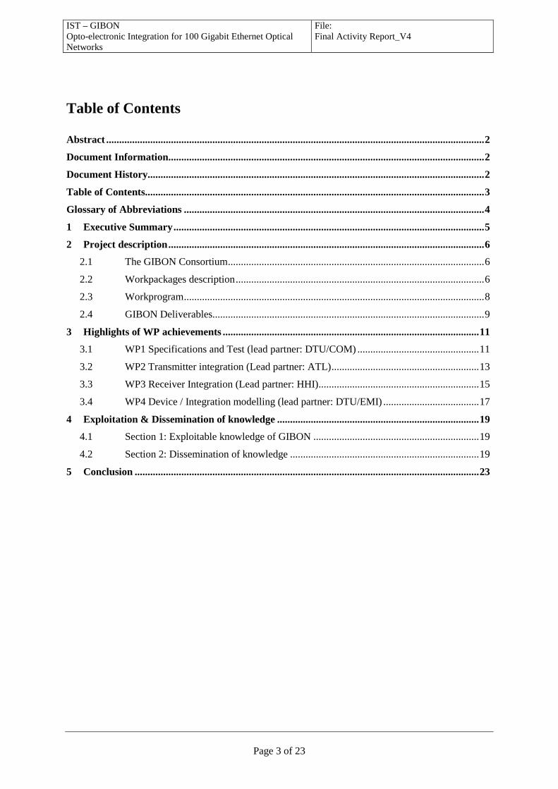
Proposal No. IST-034183
Opto-electronic Integration for 100 Gigabit Ethernet Optical Networks
Instrument type: STREP Priority name: Information Society Technologies
Final Activity Report (D24)
Period covered: from 01/05/08 to 31/07/09 Due date of Deliverable: September 15th, 2009 Start date of project: May 1st, 2006 Duration: 39 months Project Coordinator Organisation: Alcatel-Thales III-V Lab (ATL) André Scavennec Revision V4
IST – GIBON Opto-electronic Integration for 100 Gigabit Ethernet Optical Networks
File: Final Activity Report_V4
Page 2 of 23
Abstract
This Deliverable is the Final Activity Report for project GIBON, giving an overview of the objectives and achievements of GIBON.
Document Information
Status and Version: V4 Date of Issue: Dissemination level: Programme Participants Author(s): All partners GIBON Checked by: André Scavennec ATL
Document History
Version Date Authors Comment V1 September 8th, 2009 AS V2 AS, JS, TKJ, H-G.B VF September 14th 2009 Review version V4 November 3rd 2009 AS Revised version
Project co-funded by the European Commission within the Sixth Framework Programme (2002-2006)
Dissemination Level PU Public X
PP Restricted to other programme participants (including the Commission Services)
RE Restricted to a group specified by the consortium (including the Commission Services) CO Confidential, only for members of the consortium (including the Commission Services)
IST – GIBON Opto-electronic Integration for 100 Gigabit Ethernet Optical Networks
IST – GIBON Opto-electronic Integration for 100 Gigabit Ethernet Optical Networks
File: Final Activity Report_V4
Page 4 of 23
Glossary of Abbreviations
BER Bit Error Rate BERT Bit Error Rate Test set-up BCB Benzo-chloro-butene CPM Clock Phase Margin CPW CoPlanar Waveguide DC Direct Current DCF Dispersion Compensating Fibre DFB Distributed FeedBack laser DFF D-Flip-Flop DEMUX Demultiplexor DER Dynamic Extinction Ratio DUT Device Under Test EAM ElectroAbsorption Modulator EML Electroabsorption Modulated Laser ESD ElectroStatic Discharge FWHM Full Width at Half Maximum HBT Heterojunction Bipolar Transistor HEMT High Electron Mobility Transistor IC Integrated Circuit MBE Molecular Beam Epitaxy MOVPE Metal Organic Vapour Phase Deposition MZM Mach Zehnder Modulator NRZ Non Return to Zero OEIC OptoElectronic Integrated Circuit OOK On Off Keying OSNR Optical Signal to Noise Ratio OTDM Optical Time Division Multiplexing PD PhotoDiode PDL Polarisation Dispersion Loss PMD Polarisation Mode Dispersion PMMA Poly Methyl Metacrylate PRBS Pseudo Random Bit Sequence QCSE Quantum Confined Stark Effect QPSK (DP-) Quadrature Phase Shift Keying (Dual Polarization) QW Quantum Well RMS Root Mean Square RX Receiver RZ Return to Zero SDH Synchronous Digital Hierarchy SMF Single Mode Fibre SIBH Semi Insulating Buried Heterostructure TX Transmitter TWA Travelling Wave Amplifier WDM Wavelength Division Multiplexing 3R Reamplifying, Retiming, Reshaping regenerator
IST – GIBON Opto-electronic Integration for 100 Gigabit Ethernet Optical Networks
File: Final Activity Report_V4
Page 5 of 23
1 Executive Summary
GIBON was launched in the frame of IST FP6 on May 1st 2006 and was completed on July 31st 2009. The project addresses the topic of opto-electronic front ends suitable for On-Off Keying optical fibre transmission at 100 Gbit/s, as a solution to fulfil the needs of the emerging 100G Ethernet technology. During the 39 months of the project, GIBON partners have been collaborating, bringing together their broad and complementary expertise to demonstrate the viability of the proposed technical solutions: compact, Multi-Chip Modules associating very large bandwidth integrated optoelectronics devices (Electro-absorption modulated laser and pin photodiode / Travelling-Wave-Amplifier for transmitter and receiver respectively) and their driving electronics (MUX and DEMUX). While standards bodies are favouring solutions relying on -almost- available technologies for future 100G Ethernet deployments, GIBON results show that a single lane 100G OOK solution is able to ful-fil the transmission requirements.
GIBON Partners
Alcatel Thales III-V Lab France
Fraunhofer Institute for Telecommunication
Heinrich-Hertz Institute Germany
Denmark Technical University COM
Denmark
Denmark Technical University EMI
Denmark
GIBON website: www.ist-gibon.eu
IST – GIBON Opto-electronic Integration for 100 Gigabit Ethernet Optical Networks
File: Final Activity Report_V4
Page 6 of 23
2 Project description
GIBON was addressing the demonstration of very high bit rate opto-electronic transceivers suitable for 100G Ethernet applications, with the objective of demonstrating the highest speed components inte-grating the optoelectronic transducers (light modulator and photodiode) with their driving electronics (driver and preamplifier respectively). New optoelectronics components were developed based on de-signs experienced at lower bit rates and their characteristics were optimised in order to match specifi-cations derived from systems considerations. In order to reach the 100 Gbit/s objective, the integration technology for the transceivers was as impor-tant as the optoelectronic devices characteristics. Two parallel paths toward integration were followed in this project for the transmitter and receiver: monolithic integration of the laser and modulator for the transmitter, of the photodiode and electronic preamplifier for the receiver. Moreover a multi-chip inte-gration approach was then retained for the close association with the higher-speed electronic circuits, namely the selector driver and demux stage respectively. Guidelines for the design of integrated de-vices as well as for the components packaging were given by a supporting Electro-Magnetic simula-tion activity. This project was completed by an assessment of the fabricated components with respect to the projected application. To demonstrate the feasibility of transmitters and photoreceivers able to support a 100 Gbit/s OOK modulation, 4 main objectives were identified.
- Objective 1: extended bandwidth transmitting and receiving opto-electronic components, compatible with a 100G Ethernet ETDM application
- Objective 3: electro-magnetic modelling of the integration approach and large signal model-ling of HBTs for driver applications
- Objective 4: 100 Gbit/s test bench for transceivers assessment with respect to the 100G Ethernet applications
2.1 The GIBON Consortium In order to address the above objectives, complementary competences were gathered in a 4-partner Consortium:
- 1 Industrial Lab: Alcatel-Thales III-V lab, acting as prime contractor, - 1 Public Research Center: FhG Heinrich Hertz Institute, - 1 University: Denmark Technical U. contributing through 2 Departments:
o DTU-Fotonik (COM) o DTU-Elektro (EMI)
2.2 Workpackages description The different tasks identified for GIBON were carried out in 4 technical Work Packages:
• Work Package 1: Specification & test
o Based on current 10G Ethernet specifications, a first set of specifications for the transmitter and receiver was defined. These specifications were further refined, based on the measurements of experimental EML and photodiode samples.
o Modelling of single mode fibre transmission was performed in order to assess the ap-plication area for the components developed in GIBON.
o A test set-up was assembled and successfully operated for 100G characterization of the transmitter and receiver, using an optical clock transmission.
IST – GIBON Opto-electronic Integration for 100 Gigabit Ethernet Optical Networks
File: Final Activity Report_V4
Page 7 of 23
• Work Package 2: Transmitter integration o An Electro-absorption Modulated Laser was developed, based on a high modulation
efficiency AlGaInAs QW and using a short modulation section so as to allow its op-eration as a lumped device at 100 Gbit/s.
o Based on a newly available 0.7 µm InP HBT process, a specific driver, providing a 1V output swing voltage with a negative bias offset (-2.5 V) was designed and fabricated. Other high-speed mixed-signal circuits were designed including 2:1 selector and DFF acting as multiplexor and demultiplexor for their integration within Tx and Rx mod-ules.
o A Tx module was successfully designed and assembled allowing very close integra-tion of a selector/driver chip with an EML. A 2dB Dynamic Extinction Ratio was measured at 86 Gbit/s, for a -3.5 dBm average power coupled in fibre.
• Work Package 3: Receiver integration
o A very high-speed pin photodiode module was designed, exhibiting a bandwidth lar-ger than 100 GHz.
o A Receiver OEIC integrating a pin photodiode and a large bandwidth Travelling Wave Amplifier based on an InP HEMT technology was designed. Following an op-timization of the HEMT process, pin-TWA chips were successfully fabricated and packaged.
o Packaged pin and pin-TWA were also developed, with very limited bandwidth degra-dation when compared to bare dies. Moreover both devices were assembled with de-multiplexing ICs in compact Rx packages and characterized up to 107 Gbit/s, exhibit-ing a record sensitivity of 1.7 dBm.
• Work Package 4: Device / integration modelling
o 3D electromagnetic modelling was developed for characterization and optimization of the photodiode chip/output connector transition.
o DC characteristics and S-parameters of various emitter length HBTs (0.7 µm emitter width) provided inputs for the development of a scalable HBT model, used by WP2 in their driver design.
O/E Integration & Packaging
WP1
WP2
WP4
WP3Packages & (DE)MUX
Specifications & O/E models
Samples &models
Graph of interactions between WPs
IST – GIBON Opto-electronic Integration for 100 Gigabit Ethernet Optical Networks
File: Final Activity Report_V4
Page 8 of 23
The above graphic explains the main interaction between partners: While the main technological developments for the Tx and Rx were done in WP2 and WP3, with in-teractions on packaging and integration of MUX/DEMUX functions, specifications and optoelectronic characterization and testing were provided by WP1, with WP4 developing an Electromagnetic simula-tion activity for the modelling of packaging. In WP4 another activity was devoted to the large-signal scalable models of InP HBT, for the design of drivers.
2.3 Workprogram
The following graph shows the original time breakdown of the different tasks carried out in the 4 tech-nical Work Packages.
Implementation plan at the start of the project Actually the technological developments intended during the first two years of GIBON prove more difficult to master than projected, so that a 3 months extension was requested to complete the Tx and Rx chips development, their packaging and the testing of the produced modules.
GIBON Leader Semester
1 Semester
2 Semester
3 Semester
4 Semester
5 Semester
6
WP1 Specifications & Test COM
1.1 Specifications for Transcei-vers
1.2 EML with short EAM charac-teristics
1.3 pin & pin / TWA characteri-zation
1.4 100 Gb/s TX / RX assess-ment.
WP2 Transmitter Integration ATL
2.1 EML for 100 Gb/s applica-tions
2.2 HBT driver for EML
2.3 EML / Driver IC integration
WP3 Receiver Integration HHI
3.1 pin photodiode module
3.2 pin / TWA module
3.3 Receiver with DEMUX func-tion
WP4 Device / Integration Model-ling EMI
4.1 EM modelling of integration
4.2 Scalable large signal HBT model
IST – GIBON Opto-electronic Integration for 100 Gigabit Ethernet Optical Networks
File: Final Activity Report_V4
Page 9 of 23
2.4 GIBON Deliverables
Del. Deliverable name WP Nature Dissem. Delivery Date
D0 Project presentation 0 R PU 3
D1 EML with short EAM in standard module 2 P CO 4
D2 Preliminary specifications 1 R PP 6
D3 EML flip-chip process and characterization (BW>50 GHz)
2 R RE 12
D4 100 Gb/s photodiode module 3 P CO 12
D5 1st annual report 0 R PP 12
D6 Driver chip (1st design) 2 P CO 15
D7 E/O characteristics of short EAM & pin photodi-ode
1 R RE 16
D8 EML with 3 dBm output (SAG taper) 2 R RE 18
D9 Receiver comprising photodiode & DEMUX 3 P CO 18
D10 EM simulation of interconnects & device para-sitics
4 R PP 18
D11 Scalable HBT large-signal model for circuit simu-lation
4 O RE 21
D12 Pin-TWA photoreceiver module 3 P CO 24
D13 Transceivers final specifications 1 R PP 24
D14 2nd annual report 0 R PP 24
D15 Demonstration of the first TX assembly 2 P CO 27
D16 EM simulation based model of interconnects & packaging
4 O RE 30
D17 Driver chip (2nd design) 2 P RE 30
D18 Model & characteristics of EML & pin-TWA 1 R PP 30
D19 100 Gb/s EML 2 P CO 30
D20a RX module including DEMUX 3 P CO 30
IST – GIBON Opto-electronic Integration for 100 Gigabit Ethernet Optical Networks
File: Final Activity Report_V4
Page 10 of 23
D20b TX module including MUX 2 P CO 33
D21 Final report on 100 G TX / RX operation 1 R PP 36
D22 Final report: technological approach for TX & RX integration
3,2 R PP 36
D23 Third Annual Report 0 R PP 36
D24 Final Report 0 R PU 36
D25 Final Report on dissemination and raising public awareness
0 R PP 36
IST – GIBON Opto-electronic Integration for 100 Gigabit Ethernet Optical Networks
File: Final Activity Report_V4
Page 11 of 23
3 Highlights of WP achievements
This section gives the highlights of the achievements in the various Work-Packages.
3.1 WP1 Specifications and Test (lead partner: DTU/COM)
• A comprehensive simulation model has been implemented in order to investigate the transmission performance of the intended transmitter (based on an electro-absorption modulation laser, EML) and photo receiver (based on standard and travelling wave to-pologies), both for direct and optically pre-amplified receiver. Effects include:
o EML’s frequency response, absorption curve and frequency chirp o Expected 100 Gbit/s integrated driver response o Dispersion, dispersion slope, PMD and non-linear effects in fibres o Optically pre-amplified receiver, including noise, saturation and dynamic gain o Photo detector (PD) response based on module measurements o Forward-error correction (7%) emulation o Simulated results compare with reasonable accuracy to measurements, so the
model is believed to offer a high confidence level in the predictions
Expected compensated transmission and optically pre-amplified receiver for 100 (left) and FEC’ed 107 Gbit/s (right). Line shows 10-12 BER limit.
IST – GIBON Opto-electronic Integration for 100 Gigabit Ethernet Optical Networks
File: Final Activity Report_V4
Page 12 of 23
• Based on the simulations a set of tentative specifications has been proposed depending
on the intended transmission systems, e.g. compensated, uncompensated, w/ and w/o optical amplification
• Implementation of a 100 Gbit/s test-bed o MUX-EML based transmitter o PD-DEMUX based receiver o Optical clock co-propagated with modulated data o Clock recovery scheme for BER measurements at receiver
Clock recovery scheme and PD-DEMUX set-up
MUX-EML 86 Gbit/s modulated data output 86 and 43 Gbit/s demultiplexed channels af-ter 170 km SMF transmission
IST – GIBON Opto-electronic Integration for 100 Gigabit Ethernet Optical Networks
File: Final Activity Report_V4
Page 13 of 23
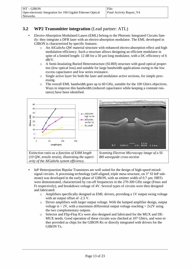
3.2 WP2 Transmitter integration (Lead partner: ATL) • Electro-Absorption Modulated Lasers (EML) belong to the Photonic Integrated Circuits fam-
ily: they integrate a DFB laser with an electro-absorption modulator. The EML developed in GIBON is characterized by specific features:
o An AlGaInAs QW material structure with enhanced electro-absorption effect and high modulation efficiency. Such a structure allows designing an efficient modulator in spite of a limited length: 12 dB for a 50 µm long modulator, with a DC efficiency of 6 dB/V.
o A Semi-Insulating Buried Heterostructure (SI-BH) structure with good optical proper-ties (low optical loss) and suitable for large bandwidth applications owing to the low excess capacitance and low series resistance.
o Single active layer for both the laser and modulator active sections, for simple proc-essing.
o The overall EML bandwidth goes up to 60 GHz, suitable for the 100 Gbit/s objectives. Ways to improve this bandwidth (reduced capacitance while keeping a constant rsis-tance) have been identified.
Extinction ratio as a function of EAM length (10 QW, tensile strain), illustrating the superi-ority of the AlGaInAs system efficiency.
Scanning Electron Microscopy image of a SI-BH waveguide cross-section
• InP Heterojunction Bipolar Transistors are well suited for the design of high-speed mixed-
signal circuits. A processing technology (self-aligned, triple mesa structure, on 3” SI InP sub-strate) was developed in the early phase of GIBON, with an emitter width of 0.7 µm. HBTs were demonstrated, characterized by cut-off frequencies in the 270-300 GHz range (Fmax and Ft respectively), and breakdown voltage of 4V. Several types of circuits were then designed and fabricated:
o Amplifiers specifically designed as EML drivers, providing a 1V output swing voltage with an output offset of -2.5 V.
o Driver amplifiers with larger output voltage. With the lumped amplifier design, output voltage is > 2V, with a maximum differential output voltage reaching > 2x2V using the two complementary outputs.
o Selector and Flip-Flop ICs were also designed and fabricated for the MUX and DE-MUX needs. Good operation of these circuits was checked at 107 Gbit/s, and were ei-ther provided as chips for the GIBON Rx or directly integrated with drivers for the GIBON Tx.
IST – GIBON Opto-electronic Integration for 100 Gigabit Ethernet Optical Networks
File: Final Activity Report_V4
Page 14 of 23
Microphotograph of the selector-driver chip. Input data and clock are coming from the pads at the top; the output signal is generated at the pad in the lower right, to ease the EML pigtail-ing. The eye diagram above is measured at 86 Gbit/s.
• Different schemes for the integration of the EML and the associated selector-driver in the
transmitter module were investigated: o In a first integration scheme, a bias T is inserted between the driver and the EML to
provide the requested bias voltage to the EML. This scheme was used for the 100 Gbit/s demonstration reported at OFC’09. However this approach is prone to possible impairments related to the 100 Gbit/s signal propagation through connectors and lines (losses and jitter).
o In the retained design, the specific driver (with output voltage offset and output pads in a corner of the die), is mounted next to the EML with a direct wire connection. This assembling approach was checked to introduce minimal losses, and a 2dB Extinction Ratio was measured at 86 Gbit/s.
Carrier with interconnected driver, EML and load resistance (above). On the right is the completed module with the 3 input con-nectors and output fiber pigtail
IST – GIBON Opto-electronic Integration for 100 Gigabit Ethernet Optical Networks
File: Final Activity Report_V4
Page 15 of 23
3.3 WP3 Receiver Integration (Lead partner: HHI) • Large bandwidth photodiodes of the waveguide type can be integrated within Photonic Inte-
grated Circuits owing to their waveguide structure; they can also be integrated with electronic preamplifiers owing to the Semi-Insulating InP substrate on which they are grown. In GIBON, such photodiodes have first been optimized for their operation at 100Gbit/s (pin mesa size, steering from the the input waveguide, input taper, electrical termination …).
Passivated waveguide-integrated photodetector with spot-size converter, termination resistor and biasing network. For 5x20 µm2 sized, AR-coated photodiodes, responsivity >0.6 A/W, bandwidth > 100GHz and
polarization loss dispersion < 0.25 dB were achieved. • pin-TWA OEIC ( OptoElectronic Integrated Circuit) photoreceivers were designed and fabri-
cated, associating a waveguide type photodiode and a 5-stage travelling wave preamplifier made in the InP HEMT technology. Specific developments were necessary to produce work-ing devices.
o Tuning the HEMT process, usually performed on the HEMT layer stack directly grown onto the SI substrate, to fit the situation of having the MOVPE grown SI wave-guide layers in between.
-0.8 -0.6 -0.4 -0.2 -0.0-1.0 0.2
100
200
300
400
500
0
600
Vgs (V)
Gm (mS/mm)
100
7550
Vds=2V
HEMT transconductance for various gate width & SEM view of the 130nm gate (upper left & right); view of the pigtailed pin-TWA OEIC & packaged photoreceiver (lower left & right)
IST – GIBON Opto-electronic Integration for 100 Gigabit Ethernet Optical Networks
File: Final Activity Report_V4
Page 16 of 23
o Defining a process suited to the non planar OEIC, in particular for the e-beam writing of the short gate (≈ 100 nm length).
o Owing to the high transconductance obtained (750mS/mm intrinsic gain before BCB passivation) the gain provided by the TWA amounted to 4.7 dB.
• By combining a high-speed photodiode and a decision Flip-Flop in a same package, a high
sensitivity demultiplexing receiver was assembled. The InP-based 1.55 µm high-speed photodiode is of the waveguide-integrated type exceeding 105 GHz bandwidth. The de-multiplexing circuit is a Decision Flip-Flop fabricated in the InP Double heterojunction process. Co-packaging the two devices in a same module greatly reduces electrical losses due to separate housings and interconnections, by roughly 6 dB. World-leading sensitivity can then be obtained (see figure below). A same approach was followed with the co-packaging of a pin-TWA OEIC and decision Flip-Flop; preliminary characterization has shown full functionality, and a 4.7 dBm sensitivity at 10-9 BER.
Co-packaging the photodetector chip and the DEMUX chip in one module housing with very short bonding wires (upper left and right) allows recovery of the tributaries without any error floor for the longest sequences, illustrating the good performance of the devices and the quality of the inte-gration process (lower graph and eye diagram). Worth noting are the record sensitivities of +1.7
dBm and + 4.7 dBm at 107 Gbit/s for PRBS of 27-1 and 231-1 respectively.
IST – GIBON Opto-electronic Integration for 100 Gigabit Ethernet Optical Networks
File: Final Activity Report_V4
Page 17 of 23
3.4 WP4 Device / Integration modelling (lead partner: DTU/EMI) • EM modelling was used to investigate the performance of packaged photodetector modules
for the Rx. Potential bandwidth limiting mechanisms have been identified and suggestions for package optimization have been proposed:
o The transition from 1mm connector to conductor backed CPW was optimized. Guide-lines for via placement for low loss, resonance free transmission to 100 GHz was given.
o A full 3D electromagnetic model of a photodetector chip, including transit-time ef-fects was developed. The EM model precisely predicts the measured characteristics of photodiode chips with different p-i-n junctions.
o A new packaged PD module with a thick CPW structure was proposed. The new module exhibits improvement in the measured bandwidth up to 100 GHz and higher relative response over 80 GHz.
• EM modelling was also used to investigate the performance of EML for the Tx. Methods were
established for the EM simulation of electrical to optical transmission properties of EMLs, both on component level and within high-frequency assemblies:
o Different EML electrode structure options were investigated and suggestions for the best one was given.
o The cause of the unwanted wave-like effect observed in the measurements of the EML in a microstrip assembly was explained using an EM/circuit co-simulation approach.
o The wirebond transition from microstrip lines to EML chip on InP was investigated. A step in ground plane height was shown to introduce little additional losses. Equivalent circuit models for wirebond transitions valid to 100 GHz were developed.
Top figure shows EM model of packaged PD module. Right figure shows the experimental re-sults for the new module exhibiting higher rela-tive response over 80 GHz.
20 40 60 80 100-7
-6
-5
-4
-3
-2
-1
0
1
Rel
ativ
e re
spon
se [d
B]
Frequency [GHz]
Original moduleNew moduleChip
IST – GIBON Opto-electronic Integration for 100 Gigabit Ethernet Optical Networks
File: Final Activity Report_V4
Page 18 of 23
• A scalable large-signal model for 0.7µm InP DHBT devices has been developed within the
GIBON project. The scalable large-signal model includes thermal effects and predicts the RF performance over bias and geometry:
o The large-signal model is based on a modified UCSD HBT model. The scalable model has been made available for both the Agilent ADS and Cadence Spectre simu-lators with slightly different features.
o In order to arrive at an accurate scalable large-signal model novel parameter extrac-tion strategies for the small-signal model of HBT devices have been developed. In particular the fixed base resistance of sub-micron InP DHBT devices proved to be er-roneously extracted using traditional methods. A novel extraction technique for the external base resistance developed within the project made the scalability of the mod-els possible.
Microphotograph of EML wirebonded onto mi-crostrip lines on ceramic substrate. The EML load is 35 Ohm.
EM-circuit co-simulation of EML u-strip assem-bly. The wave-like behaviour observed in the measurements is caused by the reflection from the load due to the excessive length of the connecting microstrip line.
Top figure shows small-signal model fitting to 110 GHz (emitter length: 10µm; Vce=1.6V, Ic=20.5mA).Right figures show the frequency performance versus current for three 0.7µm InP DHBT device geometries (emitter lengths: 5µm, 7µm, 10µm).
IST – GIBON Opto-electronic Integration for 100 Gigabit Ethernet Optical Networks
File: Final Activity Report_V4
Page 19 of 23
4 Exploitation & Dissemination of knowledge
4.1 Section 1: Exploitable knowledge of GIBON GIBON has generated a substantial amount of knowledge, which the partners are willing to exploit to a large extent in future R&D activities and projects: technological integration platforms for EAM-based Photonic Integrated Circuits and Photoreceivers for spectral-efficient transmission, but also large bandwidth packaging know-how and high bit rate transmission concepts. Another path for exploitation of GIBON results is by teaching courses benefiting from activities car-ried out in GIBON; this holds in particular for DTU partners. A third path for exploitation is through providing access to the achievements of GIBON to interested parties. - Parameters for the scalable HBT model have been determined by DTU-EMI associated with the 1.5 and 0.7 µm HBT process developed by ATL. The methodology to determine the parameters is avail-able at DTU-EMI to interested parties (contact T.K. Johansen). - The EML process has been developed at ATL for several years. During GIBON, this process was further enhanced to provide structures suitable for very high-speed operation. In the frame of the CELTIC project 100GET, EML operating at 100Gbit/s (On-Off-Keying) and packaged with a matched driver will be delivered to Alcatel-Lucent Bell Labs in Stuttgart for assessment of their 100Gbit/s NRZ transmission potential. - During GIBON, HHI happened to develop a passivation process for their very high-speed pin photo-diodes. This process has been made available to u2t, as a GIBON result. - Several 100Gbit/s mixed signal ICs (selector, full 2:1 MUX, driver, decision circuit, full DEMUX) have been developed in the course of GIBON. Ways to turn some of these ICs into commercial pack-aged prototypes is now under discussion, with one SME; other interested parties are welcome and should contact ATL (contact J. Godin). - The demultiplexing pin photodiode (or demultiplexing pin-TWA) was a notable GIBON success. Both ATL and HHI are willing to turn this achievement into commercially available prototypes. As an extension to GIBON, more sensitive demultiplexing ICs and a full 1:2 DEMUX have been designed and fabricated. Following the currently done evaluation process, prototypes will be advertised on the HHI website (contact H-G. Bach). - During the whole project, packaging of 100 Gbit/s O/E modules has been a topic of interest for ATL, HHI and DTU-EMI. I particular the later has developed a broad expertise which is now available to interested parties (contact T.K. Johansen). Finally, GIBON partners have developed a broad knowledge about 100GBit/s opto-electronic and electronic technologies; the project is now over, but each partner is working on new developments in the same technical area, and each partner is open to further enquiries from interested parties.
4.2 Section 2: Dissemination of knowledge Knowledge gained through GIBON has been disseminated by three channels: the first one is the vari-ous lessons, courses or presentations given to academic audiences by GIBON partners, using the know-how developed during the project; a second one is associated to publications or presentations during international conferences (see the following list); a third one is the GIBON website reporting on the main achievements.
IST – GIBON Opto-electronic Integration for 100 Gigabit Ethernet Optical Networks
File: Final Activity Report_V4
Page 20 of 23
1. “High-speed Miniaturized Photodiode and Parallel-fed Travelling-Wave Photodetectors Based on InP” A.Beling, H-G. Bach, G.G. Mekonnen, R.Kunkel, D. Schmidt, IEEE J. Sel.Topics in QE, Vol.13 (2007) pp 15-21.
2. “Ultra-fast Efficient Photodiodes Exceeding 100 GHz Bandwidth” H-G. Bach, Invited pa-per, Int’l Conf. on Indium Phosphide & Related Materials, May 14-18 (2007), Matsue, Japan (Proc. pp. 71-76).
3. “Wide temperature Range Operation at 43 Gbit/s of 1550 µm InGaAlAs Electroabsorp-tion Modulated Laser with Single Active Layer” A.Garreau, M-C. Cuizin, J-G. Provost, F. Jorge, A. Konczykowska, C. Jany, J. Décobert, O. Drisse, F. Blache, D. Carpentier, E. Der-ouin, F. Martin, N. Lagay, J. Landreau, C. Kazmierski, Int’l Conf. on Indium Phosphide & Re-lated Materials, May 14-18 (2007), Matsue, Japan (Proc. pp. 358-360).
4. “Performances and Self-Heating Reduction of Submicron InP/InGaAs/InP heterojunc-tion Bipolar Transistors” V. Nodjiadjim, M. Riet, P. Berdaguer, O. Drisse, E. Derouin, A. Scavennec, J. Godin, Workshop On Compound Semiconductor Devices and Circuits in Europe (WOCSDICE), May 20-23 (2007), Venice, Italy.
5. “ Photoreceivers for 100 Gbit/s applications” A. Umbach, G. Unterbörsch, H-G. Bach, C. Schubert, R. Derks, J. Sinsky, IEEE/LEOS Summer Topical Meeting on Ultra-High Data-Rate Transmission, TuE4.2, 23-25 July 2007, Portland, Oregon (USA).
6. “ High-speed Integrated Modulators and Receivers” Karl-Otto Velthaus, Heinz-Gunter Bach, invited paper, IPNRA, Salt Lake City, 2007.
7. “ Ultrafast Waveguide-integrated pin-Photodiodes and Photonic Mixers from GHz to THz Range” H-G. Bach, invited paper, paper 5.5.1, 33rd ECOC 2007 (Berlin, Germany).
8. “Semi-insulating buried heterostructure 1.55 µm InGaAlAs electro-absorption modu-lated laser with 60GHz bandwidth” Ch. Jany, Ch. Kazmierski, J. Decobert, F. Alexandre, F. Blache, O. Drisse, D. Carpentier, N. Lagay, F. Martin, E. Deroin, T. Johansen, Ch. Jiang, post deadline paper, 33rd ECOC 2007 (Berlin).
9. “EM Simulation Accuracy Enhancement for Broadband Modeling of On-Wafer Passive Components” T. Johansen, C. Jiang, D. Hadziabdic, V. Krozer, EuMIC, October 8-10, 2007, Munich, (Germany).
10. “ Optimization of Integrated Electro-Absorption Modul ated Laser Structures for 100 Gbit/s Ethernet Using Electromagnetic Simulation” T. Johansen, C. Kazmierski, C. Jany, C. Jiang, V. Krozer, IMOC 2007, November, Salvador, Brazil.
12. “Optimization of Packaging PIN Photodiode Modules for 100 Gbit/s Ethernet Applica-tions” C. Jiang, G.G. Mekonnen, T. Johansen, V. Krozer, H-G. Bach, APMC 2007, December, Bangkok, Thailand.
13. “Parallel-fed Traveling Wave Photodetector for > 100 GHz Applications” A. Beling, J.C. Campbell, H-G. Bach, G.G. Mekonnen, and D. Schmidt, IEEE J. Lightwave Techn. Vol.26 (2008) pp 16-20.
14. “ A 107-Gbit/s Opto-Electronic Receiver Utilizing Hybrid Integration of a Photodetector and Demultiplexer” J.H. Sinsky, A. Adamiecki, L. Buhl, G. Raybon, P. Winzer, O. Wohlgemuth, M. Duelk, C.R. Doerr, A. Umbach, H-G. Bach, D. Schmidt, IEEE J. Lightwave Techn. Vol.26 (2008) pp 114-120.
15. “ A high conversion gain Q-band InP DHBT sub-harmonic mixer using LO frequency dou-bler” T.K.Johansen, J.Vikjaer, V.Krozer, A.Konczykowska, M.Riet, F.Jorge, T.Djurhuus, IEEE Trans. Microwave Theory and Techn. Vol56 (2008) pp 613-619.
IST – GIBON Opto-electronic Integration for 100 Gigabit Ethernet Optical Networks
File: Final Activity Report_V4
Page 21 of 23
16. “ Integration potential of Waveguide-integrated Photodiodes: self-powered Photodetectors and sub-THz pin-Antennas” H-G.Bach, R.Kunkel, G.G.Mekonnen, D.Pech, T.Rosin, D.Schmidt, T.Gaertner, R.Zhang, OFC/NFOEC, Feb 24-28, 2008, San Diego (USA).
17. “ 43 Gb/s operation of a directly connected driver and electro-absorption modulated la-ser for low-cost packages” A.Konczykowska, M.Riet, F.Jorge, F.Blache, C.Jany, J.Décobert, F.Alexandre, C.Kazmierski, OFC/NFOEC, Feb 24-28, 2008, San Diego (USA).
18. “ Improved Extrinsic Base Resistance Extraction for InP DHBT devices” T. Johansen, V. Krozer, V. Nodjiadjim, A. Konczykowska, J.-Y. Dupuy, German Microwave Conference, Ham-burg, Germany, March 2008.
19. “ Wireless and photonic high-speed communication technologies for over 100-G applications” A. Konczykowska, V.Krozer, MIKON, 19-23 May (2008) Wroclaw, Invited plenary presenta-tion.
20. “ Millimeter-wave and High-speed MMIC design, interconnects and packaging” T.K. Johansen, C. Jiang, D. Hadziabdic, V. Krozer, Session WMK on High-speed electronic tech-nologies for 100-G communications, Int’l Microwave Conference, Atlanta (USA), June 15-20 (2008).
21. “ Preliminary specifications for 100Gigabit Optical Ethernet” M. Berger, J. Seoane, C. Jespersen, L. Dittman, Proceedings of Applied Electromagnetics, Wireless and Optical Com-munications (Electroscience’08) Trondheim (Norway), July 2-4 (2008).
22. “ High-speed AlGaInAs Electroabsorption Modulated Laser with Optically Equalized Error-Free Operation at 86 Gb/s” C. Kazmierski, C. Jany, J. Décobert, F. Alexandre, F. Blache, A. Scavennec, P.J. Winzer, C.R. Doerr, G. Raybon, A. Adamiecki, T. Johansen, Euro-pean Conference on Optical Communications, Brussels (Belgium) Sept. 21-25 (2008).
23. “ InP Waveguide-integrated pin-Photodiode Hybrid Packaged with an HBT-DEMUX-Chip for Receiver Modules of 80-100 Gb/s Data Rates” G.G. Mekonnen, B. Hüttl, H-G. Bach, D. Pech, T. Rosin, C. Schubert, A. Konczykowska, F. Jorge, M. Riet, European Confer-ence on Optical Communications, Brussels (Belgium) Sept. 21-25 (2008)
24. “ Submicron InP DHBT technology for high-speed, high-swing mixed signal ICs” J.Godin, V. Nodjiadjim, M. Riet, P. Berdaguer, O. Drisse, E. Derouin, A. Konczykowska, J. Moulu, J-Y. Dupuy, F. Jorge, J-L. Gentner, A. Scavennec, T. Johansen, V. Krozer, Compound Semiconductors IC Symposium, Monterey (USA) October 12-15 (2008).
25. “ High speed Photodetectors: Self-Biasing and High-Power Behaviour” , H.-G. Bach, invited talk at the 214th Meeting of The Electrochemical Society”, Honolulu (Hawaii) October 12-17 (2008).
26. “ A technological platform for 10-100G photonic sources” Ch. Kazmierski, Invited talk at the OSA Annual meeting, Frontiers in Optics, Rochester (USA) October 19-23 (2008)
27. “ Packaging aspects of Photodetector Modules for 100 Gbit/s Ethernet Applications” C. Jiang, G.G. Mekonnen, V. Krozer, T.K. Johansen, H-G. Bach, EuMiC, Amsterdam, The Neth-erlands, Oct. 27-31 (2008).
28. “Analysis of Hybrid-Integrated High-Speed Electro-Absorption Modulated Lasers Based on EM/Circuit Co-simulation” , T. K. Johansen, V. Krozer, C. Kazmierski, C. Jany, F. Bla-che and C. Jiang, accepted for oral presentation at IEEE MTT-S International Microwave Workshop on Signal Integrity and High-Speed Interconnects, Guadalajara, Mexico, Feb. 2009.
29. “100Gb/s Operation of an AlGaInAs Semi-Insulating Buried Heterojunction EML” C. Kazmierski, A. Konczykowska, F. Jorge, F. Blache, C. Jany, A. Scavennec, OFC/NFOEC March 22-26, 2009, San Diego (USA).
30. “Demultiplexing Photoreceivers Comprising pin- and pin TWA Frontends for 107 Gbit/s ETDM” H-G. Bach, G.G. Mekonnen, R. Kunkel, C. Schubert, D. Pech, T. Rosin, A. Konc-zykowska, F. Jorge, A. Scavennec, M. Riet, OFC/NFOEC, March 22-26, 2009, San Diego (USA).
IST – GIBON Opto-electronic Integration for 100 Gigabit Ethernet Optical Networks
File: Final Activity Report_V4
Page 22 of 23
31. “Large Bandwidth Detectors and Receivers for Telecom and Wireless” H-G. Bach, invited paper, European Workshop on Photonic Solutions for Wireless, Access and in-House Net-works, Duisburg 18-20 May 2009
32. “Demultiplexing Photoreceivers Comprising pin- and pinTWA Frontends for 107 Gbit/s ETDM” H-G. Bach, G.G. Mekonnen, R. Kunkel, C. Schubert, D. Pech, T. Rosin, A. Konc-zykowska, F. Jorge, A. Scavennec, M. Riet, European Workshop on Photonic Solutions for Wireless, Access and in-House Networks, Duisburg 18-20 May 2009
33. “IST-GIBON” C. Kazmierski, A. Konczykowska, F. Jorge, F. Blache, C. Jany, J. Godin, A. Scavennec, H-G. Bach, G.G. Mekonnen, R. Kunkel, D. Schmidt, A. Seeger, D. Pech, M. Ber-ger, J. Seoane, C. Jespersen, V. Krozer, T.K. Johansen, C-H. Jiang, oral & poster presenta-tions, European Workshop on Photonic Solutions for Wireless, Access and in-House Net-works, Duisburg 18-20 May 2009
34. “Hybrid Co-Packaged Receiver Module with pin-Photodiode Chip and DEMUX-IC for 107 Gb/s Data rates” G.G. Mekonnen, H-G. Bach, R. Kunkel, C. Schubert, D. Pech, T. Rosin, A. Konczykowska, F. Jorge, A. Scavennec, M. Riet, ECOC, Vienna, Septembre 2009
35. “Packaging of Photodetector Modules for 100Gbit/s Applications Using Electromagnetic Simulations ” C. Jiang, , V. Krozer, H-G. Bach, G.G. Mekonnen, T.K. Johansen, EuMC, Rome, Italy, Septembre 2009.
36. “Electro-absorption modulator laser for cost-effective 40 Gb/s networks with low drive voltage, chirp and temperature dependence” G. Aubin, J. Seoane, K. Merghem, M.S. Ber-ger, C.F. Jespersen, A. Garreau, F. Blache, C. Jany, J-G. Provost, C. Kazmierski, P. Jeppe-sen, Electron. Letters (accepted for publication).
37. “ InP DHBT selector-driver with 2x2.7 V swing for 100Gbit/s operation” A. Konc-zykowska, J-Y. Dupuy, F. Jorge, M. Riet, J. Moulu, J. Godin, Electron. Letters (accepted for publication)
IST – GIBON Opto-electronic Integration for 100 Gigabit Ethernet Optical Networks
File: Final Activity Report_V4
Page 23 of 23
5 Conclusion
In the last three years, significant achievements were reported by GIBON, in the area of packaged opto-electronic components for 100 Gbit/s NRZ transmission.
- High-speed optoelectronic transmitters: beyond the first report by GIBON of an EML operat-ing at 100 Gbit/s at last OFC, a major achievement was the demonstration of a suitable pack-aging technology. The performance achieved (2dB extinction ratio) was limited by the mis-match between the DC characteristics of EML and driver.
- High-speed optoelectronic receivers: very high-speed packaged photodiodes with suitable bandwidth and responsivity have been developed, as well as photodetectors with internal gain provided by an integrated TWA. Moreover demultiplexing photoreceivers were developed, and error-free operation demonstrated at 107 Gbit/s.
- Associated microelectronics: GIBON achievements in high-voltage driver amplifiers based on the InP HBT are also world-leading results.
These achievements are resulting from the close collaboration of partners within GIBON, and the pro-ject was instrumental in reaching such results. While first standards are expected soon, regarding 100G Ethernet and related technologies, trends are towards using available technologies for client interfaces: 10x10 Gbit/s or more likely 4x25 Gbit/s in a multilane approach, or high spectral efficiency coding (e.g. DP-QPSK) for line transport (OIF recently retained DP-QPSK for long haul DWDM transmission). However it was shown through the GIBON project, that 100 Gbit/s OOK transmission has a real potential for transmission over spans of several tens of km. The inherent simplicity of the OOK modulation scheme is still a strong and actual reason to further develop this technology for future standardisation and deployment.