Jong Hyeok Park,†,‡ Tae-Woo Lee,⊥ and Jeong Ho Cho*,†,‡
†SKKU Advanced Institute of Nanotechnology (SAINT), ‡School of Chemical Engineering, §School of Advanced Materials Scienceand Engineering, Sungkyunkwan University, Suwon 440-746, Republic of Korea∥Materials Research Center, Samsung Advanced Institute of Technology (SAIT), Suwon 443-803, Republic of Korea⊥Department of Materials Science and Engineering, Pohang University of Science and Technology (POSTECH), Pohang 790-784,Republic of Korea
*S Supporting Information
ABSTRACT: We propose a novel approach to fabricatingflexible transparent metallic grid electrodes via evaporativedeposition involving flow-coating. A transparent flexible metalgrid electrode was fabricated through four essential stepsincluding: (i) polymer line pattern formation on the thermallyevaporated metal layer onto a plastic substrate; (ii) rotation ofthe stage by 90° and the formation of the second polymer linepattern; (iii) etching of the unprotected metal region; and (iv)removal of the residual polymer from the metal grid pattern.Both the metal grid width and the spacing were systematicallycontrolled by varying the concentration of the polymer solution and the moving distance between intermittent stop times of thepolymer blade. The optimized Au grid electrodes exhibited an optical transmittance of 92% at 550 nm and a sheet resistance of97 Ω/sq. The resulting metallic grid electrodes were successfully applied to various organic electronic devices, such as organicfield-effect transistors (OFETs), organic light-emitting diodes (OLEDs), and organic solar cells (OSCs).
Transparent conductors are a key component in a variety ofoptoelectronic devices, including liquid crystal displays(LCDs),1,2 organic light emitting diodes (OLEDs),3,4 organicsolar cells (OSCs),5,6 and touch screens.7,8 Indium tin oxides(ITOs) are the most widely used transparent conductingmaterials due to their excellent optical transparency and highelectrical conductivity; however, the high cost of ITO, thescarcity of indium, and the fragility of the material presentsignificant drawbacks to the use of ITO in next-generationelectronic applications.7,9 Recent efforts have focused on thedevelopment of alternative transparent carbon-based conduc-tors based on carbon nanotubes (CNTs),10,11 graphene,7,12−14
or conducting polymers;15,16 however, the conductivity of suchalternative conductors is highly sensitive to the samplefabrication process and is insufficient for many optoelectronicapplications. Another class of transparent conductor is derivedfrom metallic nanowires.9,17−20 Silver nanowire net-works,17,21−23 in particular, have been extensively explored fortheir potential utility in optoelectronic devices because of theirlow fabrication costs, high conductivity, transparency, andflexibility; however, silver nanowire networks suffer fromseveral problems, such as the difficulty of developing a uniformnanowire distribution on a substrate, the significant roughness
of the networks, inferior electrical contact among thenanowires, and delamination of the nanowires from a substrate.Recently, metallic mesh-type electrodes have also beenexplored as promising alternatives because both their sheetresistance and their optical transmittance are easily controlledby varying the grid width, spacing, and thickness.24−29 Anotheradvantage is the reduced junction resistance of the mesh-typestructure, which results from the formation of continuouselectrical pathway based on the metal grid lines crossing oneanother. In addition, the work function of the electrode can besimply tuned by changing the metallic materials.To form metallic grid electrodes, typical methods involve
vacuum deposition of metal films followed by the photo-lithography, nanoimprint lithography (NIL), or transferprinting.29−31 As an alternative, using of evaporative self-assembly of nanomaterials through flow-coating can be a simpleroute to form patterns. This method relies on controlling thestick−slip motion at a three-phase (atmosphere−liquidsolution−substrate) contact line. Based on the method, theLin group has demonstrated a wide variety of patterns of
polymers, nanocrystals, nanoparticles, nanorods, and evenDNA.32−34 Also, the Crosby group has recently demonstratedwell-aligned patterns of nanoparticles (metallic or semi-conducting) by controlling evaporation using a polymericblade.35−37 Accordingly, formation of highly uniform metallicgrid patterns should be possible through the method. Inprinciple, this method should be readily applied to large areasubstrates and allow tuning the line width and the spacing ofthe grid electrodes precisely, despite the avoidance ofphotolithographic processes but only through careful materialselection and tuning processing parameters.In these lines, we herein demonstrate the fabrication of
flexible transparent metallic grid electrodes via evaporativedeposition involving flow-coating applicable to the productionof various high-performance organic electronic devices. Theprocess included establishing a cross-line pattern of polymerson a metallic film via flow-coating, followed by the removal ofboth the unprotected metal and residual polymer on themetallic pattern. Metallic grid patterns were prepared withdifferent grid widths and spacings by controlling theconcentration of the polymer solution and the moving distancebetween intermittent stop times of the polymer blade. Theoptimized Au grid electrodes exhibited an optical transmittance
of 92% at 550 nm and a sheet resistance of 97 Ω/sq. Themetallic grid electrodes exhibited excellent mechanical flexibilitycompared to the flexibilities of metallic films and ITO. Themetallic grid electrodes were successfully used as electrodematerials in various organic electronic devices, such as organicfield-effect transistors (OFETs), organic light-emitting diodes(OLEDs), and organic solar cells (OSCs).
2. EXPERIMENTAL SECTIONFabrication of Metallic Grid Electrode. Polystyrene (PS)
solutions having a range of concentrations (1.5−10 mg/mL) wereprepared by dissolving PS (Mw = 192 000) in toluene. The solutionwas stirred for 24 h. All PS solutions were filtered through apolytetrafluoroethylene (PTFE) membrane with a pore size of 0.5 μmprior to flow-coating. A 200 μm thick polyethylene terephthalate(PET) film was cleaned with acetone, isopropanol, and deionizedwater sequentially, followed by drying under a nitrogen stream. A 90nm thick Au layer was thermally deposited onto the cleaned PET film.
The flow-coating setup consisted of an angled polymer bladeattached to a vertical translation stage and linear translation stageattached to a piezo nanopositioner (Physik Instrumente (PI) GmbH &Co. KG) as shown in Figure 1a. The metal-deposited PET films werefixed on the linear translation stage. A 75 μm thick PET blade that wasscored 1.2 mm from the edge was attached rigidly at a 60° angle
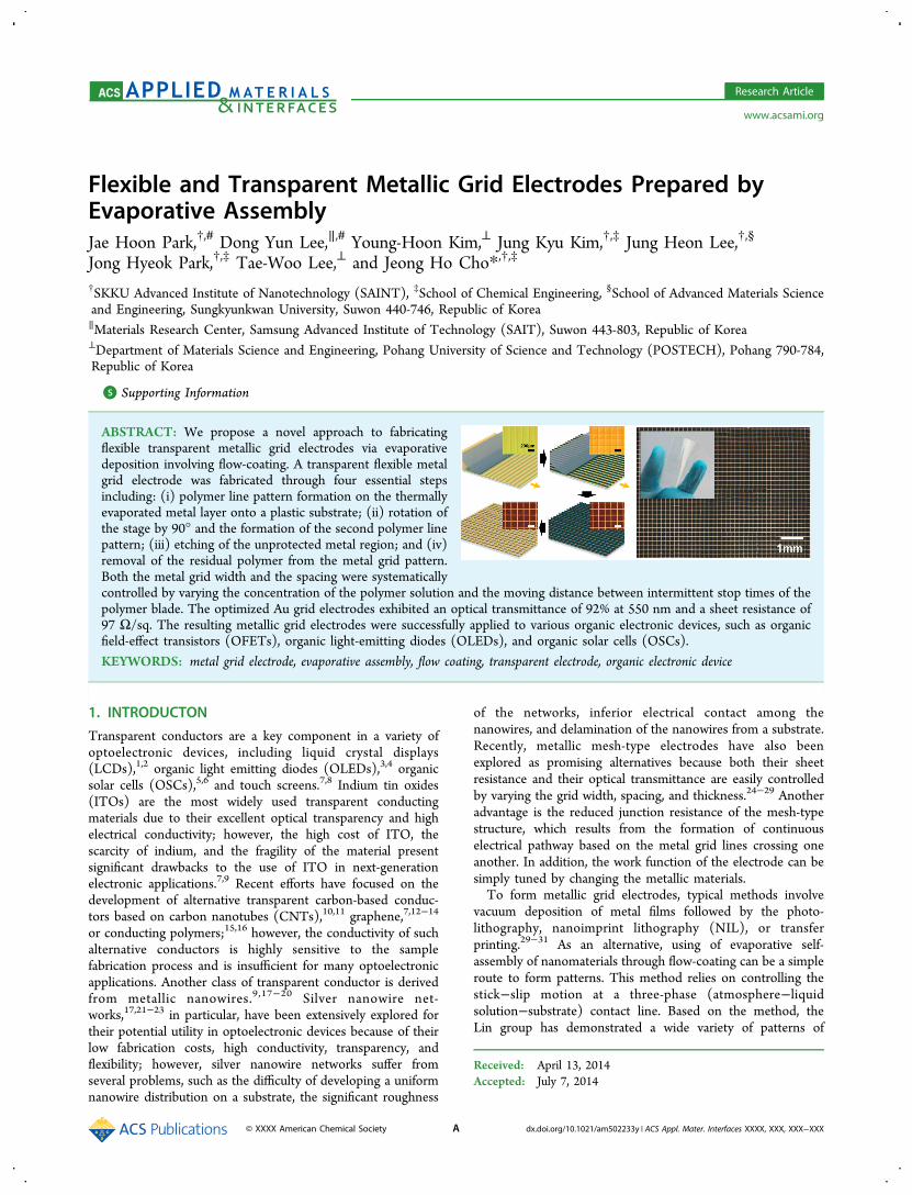
Figure 1. (a) Photographic image of the home-built flow-coating setup. The machine included a lateral translation stage attached to a piezonanopositioner and a polymer blade attached to a vertical translation stage. The inset shows an enlarged image of the polymer solution trapped bycapillary forces between the polymer blade and the substrate. The yellow arrow indicates the direction of motion of the lateral translation stage. (b)Schematic illustration of the formation of the PS line pattern. Lower panel shows the velocity of the linear translation stage as a function of time. (c)Schematic procedure for fabricating the metallic grid electrodes. The process includes (i) forming polymer line patterns on a thermally evaporatedmetal substrate and exposing the polymer patterns to UV illumination to cross-link the patterned polymer; (ii) polymer line pattern formation on thetwisted substrate; (iii) etching away the unprotected metal; (iv) removing the polymer pattern. (d) Photographic and OM images of the flexibletransparent Au grid electrodes with a grid width of 4.5 μm and a grid spacing of 200 μm (Au thickness ∼90 nm). (e) Optical transmittance as afunction of the wavelength. The inset shows an optical image of the Au grid electrodes.
ACS Applied Materials & Interfaces Research Article
relative to the vertical translation stage. The mounting configurationpermitted rotational alignment. The PET blade was then brought intocontact with the substrate. A PS solution in toluene was then injectedbetween the PET blade and substrate. Due to the capillary forces, theinjected solution became trapped at the thinnest regime between theblade and substrate, as shown in Figure 1b. Over a period of timethrough which the linear translation stage beneath the substrateremained stationary, evaporation of toluene (red arrow in the figure)led migration of nonvolatile PS molecules to the air/solution/substratecontact edge (blue arrow in the figure) and subsequent line depositionof the molecules. As the underneath stage was moved by a certaindistance after a given period of time, the meniscus at the air/liquidinterface was stretched and the contact angle at this interface wasreduced. When the contact angle fell below the critical receding angle,the capillary force exceeded the pinning force and dragged the air/solution/substrate contact edge to a new position. Consequently, thecontact angle was recovered to initial value and a new PS line patternwas formed upon subsequent evaporation of toluene. The stop andmoving of the linear translation stage were controlled through ahomemade software program with variable moving distance, movingvelocity, and intermittent stop time.The transparent and flexible metal grid electrode was fabricated as
follows: (i) the PS line patterns were formed on the thermallyevaporated Au layer on the PET surface, and UV exposure (254 nm,28 mW/cm2, 5 min) cross-linked the PS; (ii) the stage was rotated by90°, and a second PS line pattern was formed; (iii) the unprotected Auregions were etched with KI (28 Å/s, 20 s); and (iv) the PS gridpattern was removed using reactive ion etching (100 W, 20 sccm, and60 s). The transmittance and sheet resistance of the Au grid films werecharacterized by UV−visible spectrophotometry (Agilent 8453) andthe four-point probe technique using Keithley 2182A and 6221 units,respectively.Both sheet resistance (Rs) and optical transmittance (TAu‑grid) of the
metallic grid electrodes could be estimated from the followingequations:38,39
ξρ
= −
−R
t f1
sAu grid
Au grid F
= −−T f100(1 )Au grid F2
Here, ξ is a correction factor that can be obtained by fitting theexperimental data. ρAu‑grid is the resistivity of the Au grid. tAu‑grid is thethickness of the Au grid. f F is the filling factor defined as f F = W/(D+W), where D and W are grid spacing and width of the electrodes,respectively.Fabrication of OFETs. Polyethylene terephthalate (PET) coated
with indium tin oxide (ITO) (Fine Chemical Industry Inc., Korea) wasused as a plastic substrate for fabricating bottom-contact, bottom-gatepentacene FETs. The ITO surface was then cleaned with UV-ozonetreatment (254 nm, 28 mW/cm2) for 30 min. A dimethylformamidesolution comprising 10 wt % poly-4-vinylphenol (PVP, Mw = 20,000 gmol−1) and 5 wt % poly(melamine-co-formaldehyde) (PMF, Mw = 511g mol−1) was spin-cast onto an ITO/PET substrate. The substrate wasthen annealed thermally for 12 h at 80 °C in a vacuum oven to cross-link the polymer. The specific capacitance of the cross-linked PVP(cPVP) gate dielectric (thickness = 503 nm) was 7.1 nFcm−2. A Aulayer (thickness = 50 nm) was then thermally deposited onto the cPVPsurface through a shadow mask, followed by the aforementionedpatterning steps. The channel length and width were 50 and 1000 μm,respectively. Finally, 50 nm thick pentacene (Aldrich Chemical Co., nopurification) films were deposited onto the channel region from aquartz crucible onto the cPVP substrates at a rate of 0.2 Ås−1 using anorganic molecular beam deposition (OMBD) system. The electricalcharacteristics of the OFETs were measured at room temperatureunder ambient conditions in a dark environment using Keithley 2400equipment and 236 source/measure units.Fabrication of OLEDs. Au grids electrodes with a grid width of 4.5
μm and a grid length of 150 μm were prepared onto polyethylenenaphthalate [PEN (thickness = 125 μm), Plastic Films Co., Ltd.]. A
PEN substrate coated with ITO (13 Ω/sq) was purchased by PeccellTechnologies, Inc. Onto the Au grids electrde, CVD-grown singlelayer graphene was transferred. Experimental details of the graphenesynthesis and transfer was described in Supporting Information. Ontothe prepared Au grids, Au grids/graphene, and ITO electrodes, 22 nmthick ZnO were deposited by sputtering. After UV-ozone treatment(254 nm, 28 mW/cm2) for 10 min, a polyethylene imine (PEI, Sigma-Aldrich) dissolved in 2-methoxyethanol was spin-cast onto ZnO toform 10 nm film and then was dried at 100 °C for 10 min in ambientcondition. The substrates were then transferred into a N2 glovebox,and Super Yellow (Merck OLED Materials. GmbH, catalog numberPDY-132) dissolved in toluene (0.9 wt %) was spin-cast onto the PEIlayer (thickness of Super Yellow = 230 nm). The structure was thenbaked at 80 °C for 20 min. The specimen was transferred into a high-vacuum chamber (<10−7 Torr). Finally, 5 nm thick MoO3 (powder,99.99%, Sigma-Aldrich) and 80 nm thick Ag were deposited bythermal evaporation. The current−voltage−luminance characteristicswere measured using a Keithley 236 source measurement unit and aMinolta CS2000 Spectroradiometer.
Fabrication of OSCs. The prepared Au grids, Au grids/graphene,and ITO electrodes were cleaned with acetone, 2-propanol, acetone,and 2-propanol in a sonic bath. UV−ozone treatment was thenperformed for 10 min. A 200 nm thick PEDOT:PSS (AI4083, OssilaLtd.) hole conducting layer was spin-cast onto the UV-ozone-treatedAu grids, Au grids/graphene, and ITO electrodes (2000 rpm, 1 min).The samples were then baked at 115 °C for 15 min on a hot plate. Abulk heterojunction (BHJ) layer was spin-cast onto the PEDOT:PSSlayer. The solution was prepared by dissolving poly({4,8-bis[(2-ethylhexyl)oxy]benzo[1,2-b:4,5-b′]dithiophene-2,6-diyl}{3-fluoro-2-[(2-ethylhexyl)carbonyl]thieno[3,4-b]thiophenediyl}) (PTB7) and[6,6]-phenyl C71 butyric acid methyl ester (PC71BM) in a 1:1.5weight ratio in 3% diiodooctane-containing chlorobenzene solvent. A 6nm thick TiOx layer was coated onto the BHJ layer. The TiOx solutionwas prepared by adding titanium isopropoxide (TIP) (80 g) intomethanol (80 g). Glacial acetic acid (16 g) was then added to thesolution. After vigorous stirring for 30 min, 5 mL of water was droppedinto the solution. The TiOx solution was stored at room temperaturefor over 12 h prior to the spin-coating. Finally, a 100 nm thick Alcathode was thermally evaporated under 10−7 Torr. The J−Vperformances of the OSCs were measured using an Oriel 91193 (1kW lamp, 100 mW/cm2) device, an NREL-calibrated Si solar cell, andKeithley 2400 source meters. A 11.43 mm2 aperture was used todetermine the cell area. The incident photon-to-current efficiency(IPCE) measurements were conducted using a Solar Cell QE/IPCE(Zolix Solar Cell Scan 100).
3. RESULTS AND DISCUSSION
Figure 1a shows photographic images of the flow-coating setup,in which an angled polymer blade is attached to a verticaltranslation stage and a linear translation stage is attached to apiezo nanopositioner.36,37 The polyethylene terephthalate(PET) blade was brought into contact with the thermallydeposited Au layer (90 nm thick) on a PET substrate. The PETblade was scored 1.2 mm from the edge, which preventedhinging and increased the conformal contact with the substrate,as shown in the inset of Figure 1a and b. A polystyrene (PS)solution was introduced between the PET blade and thesubstrate and was trapped by capillary forces. When the lineartranslation stage was stationary over a period of stopping time,the evaporation of toluene (red arrow) induced migration (bluearrow) and deposition of PS near the contact line (upper panelof Figure 1b).40 Subsequently, the linear translation stage wasmoved by a certain distance. The movement of the lineartranslation stage stretched the meniscus until the contact anglefell below the critical receding angle, at which point thecapillary force exceeded the pinning force and the contact lineslipped to a new position. As a result, the contact angle was
ACS Applied Materials & Interfaces Research Article
recovered to initial value, leaving behind a new PS line. Thelinear translation stage was moved through a programmedmoving distance between intermittent stop times (1 s) at afixed velocity (1.5 mm/s), as shown in the lower panel ofFigure 1b. The line width and spacing could be controlled byvarying the stop time and the moving distance, respectively.A transparent flexible metal grid electrode was fabricated
through four essential steps, including (i) PS line patternformation on the thermally evaporated Au layer mounted on aPET substrate, followed by UV exposure to enable PS cross-linking; (ii) rotation of the stage by 90° and the formation ofthe second PS line pattern; (iii) etching of the unprotected Auregion with KI; and (iv) removal of the residual PS from the Augrid pattern using reactive ion etching (RIE). A schematicdiagram and the optical microscopy (OM) images of each stepare shown in Figure 1c. Figure 1d shows photographic and OMimages of the flexible transparent Au grid electrodes with a gridwidth of 4.5 and a grid spacing of 200 μm, produced by flow-coating. The optical transmittance of the resulting Au gridelectrodes remained nearly constant over the entire visiblewavelength range covering 400−800 nm (Figure 1e). Theoptical transmittance at 550 nm and the sheet resistance werefound to be 95% and 128 Ω/sq, respectively.Both the optical transmittance and the sheet resistance could
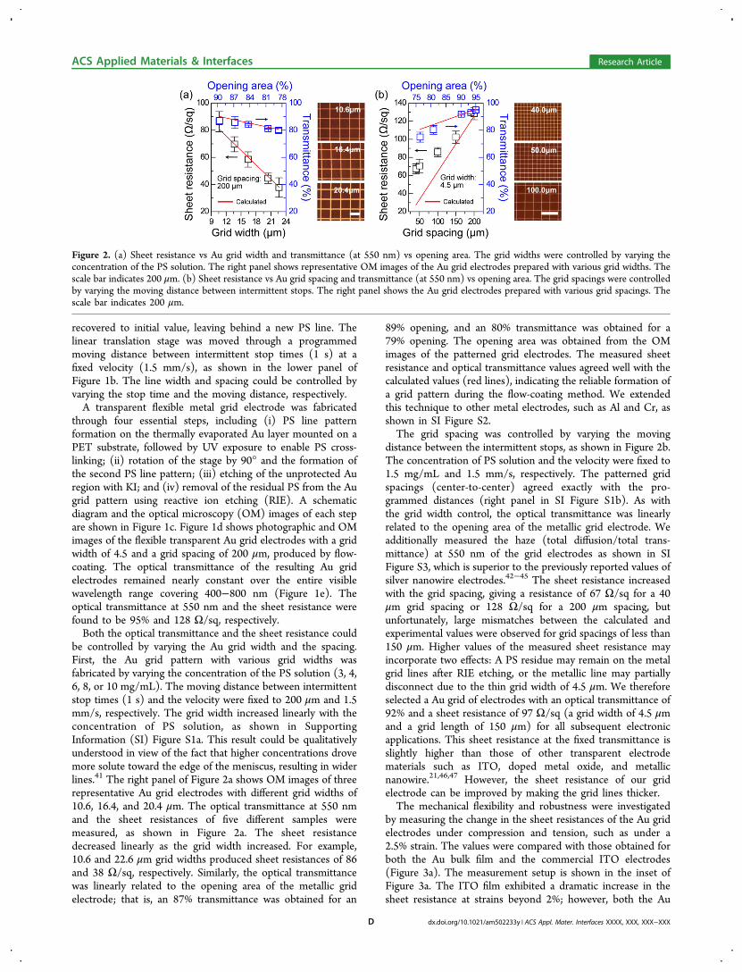
be controlled by varying the Au grid width and the spacing.First, the Au grid pattern with various grid widths wasfabricated by varying the concentration of the PS solution (3, 4,6, 8, or 10 mg/mL). The moving distance between intermittentstop times (1 s) and the velocity were fixed to 200 μm and 1.5mm/s, respectively. The grid width increased linearly with theconcentration of PS solution, as shown in SupportingInformation (SI) Figure S1a. This result could be qualitativelyunderstood in view of the fact that higher concentrations drovemore solute toward the edge of the meniscus, resulting in widerlines.41 The right panel of Figure 2a shows OM images of threerepresentative Au grid electrodes with different grid widths of10.6, 16.4, and 20.4 μm. The optical transmittance at 550 nmand the sheet resistances of five different samples weremeasured, as shown in Figure 2a. The sheet resistancedecreased linearly as the grid width increased. For example,10.6 and 22.6 μm grid widths produced sheet resistances of 86and 38 Ω/sq, respectively. Similarly, the optical transmittancewas linearly related to the opening area of the metallic gridelectrode; that is, an 87% transmittance was obtained for an
89% opening, and an 80% transmittance was obtained for a79% opening. The opening area was obtained from the OMimages of the patterned grid electrodes. The measured sheetresistance and optical transmittance values agreed well with thecalculated values (red lines), indicating the reliable formation ofa grid pattern during the flow-coating method. We extendedthis technique to other metal electrodes, such as Al and Cr, asshown in SI Figure S2.The grid spacing was controlled by varying the moving
distance between the intermittent stops, as shown in Figure 2b.The concentration of PS solution and the velocity were fixed to1.5 mg/mL and 1.5 mm/s, respectively. The patterned gridspacings (center-to-center) agreed exactly with the pro-grammed distances (right panel in SI Figure S1b). As withthe grid width control, the optical transmittance was linearlyrelated to the opening area of the metallic grid electrode. Weadditionally measured the haze (total diffusion/total trans-mittance) at 550 nm of the grid electrodes as shown in SIFigure S3, which is superior to the previously reported values ofsilver nanowire electrodes.42−45 The sheet resistance increasedwith the grid spacing, giving a resistance of 67 Ω/sq for a 40μm grid spacing or 128 Ω/sq for a 200 μm spacing, butunfortunately, large mismatches between the calculated andexperimental values were observed for grid spacings of less than150 μm. Higher values of the measured sheet resistance mayincorporate two effects: A PS residue may remain on the metalgrid lines after RIE etching, or the metallic line may partiallydisconnect due to the thin grid width of 4.5 μm. We thereforeselected a Au grid of electrodes with an optical transmittance of92% and a sheet resistance of 97 Ω/sq (a grid width of 4.5 μmand a grid length of 150 μm) for all subsequent electronicapplications. This sheet resistance at the fixed transmittance isslightly higher than those of other transparent electrodematerials such as ITO, doped metal oxide, and metallicnanowire.21,46,47 However, the sheet resistance of our gridelectrode can be improved by making the grid lines thicker.The mechanical flexibility and robustness were investigated
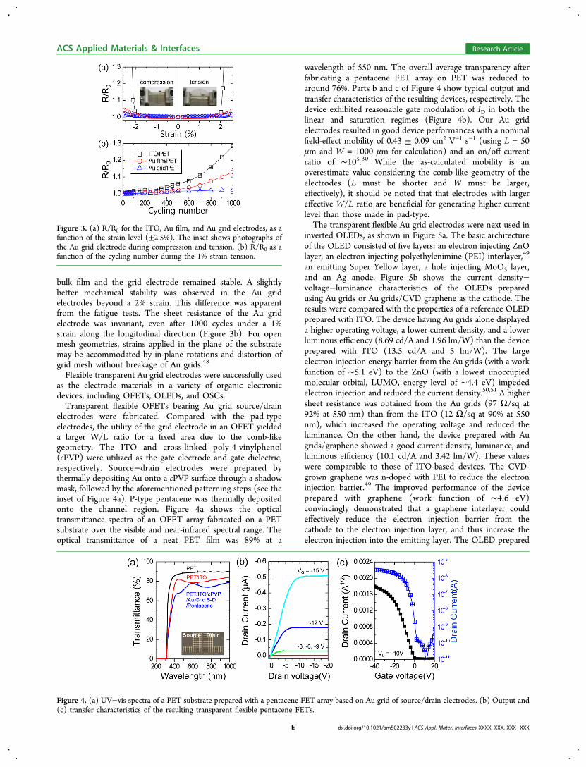
by measuring the change in the sheet resistances of the Au gridelectrodes under compression and tension, such as under a2.5% strain. The values were compared with those obtained forboth the Au bulk film and the commercial ITO electrodes(Figure 3a). The measurement setup is shown in the inset ofFigure 3a. The ITO film exhibited a dramatic increase in thesheet resistance at strains beyond 2%; however, both the Au
Figure 2. (a) Sheet resistance vs Au grid width and transmittance (at 550 nm) vs opening area. The grid widths were controlled by varying theconcentration of the PS solution. The right panel shows representative OM images of the Au grid electrodes prepared with various grid widths. Thescale bar indicates 200 μm. (b) Sheet resistance vs Au grid spacing and transmittance (at 550 nm) vs opening area. The grid spacings were controlledby varying the moving distance between intermittent stops. The right panel shows the Au grid electrodes prepared with various grid spacings. Thescale bar indicates 200 μm.
ACS Applied Materials & Interfaces Research Article
bulk film and the grid electrode remained stable. A slightlybetter mechanical stability was observed in the Au gridelectrodes beyond a 2% strain. This difference was apparentfrom the fatigue tests. The sheet resistance of the Au gridelectrode was invariant, even after 1000 cycles under a 1%strain along the longitudinal direction (Figure 3b). For openmesh geometries, strains applied in the plane of the substratemay be accommodated by in-plane rotations and distortion ofgrid mesh without breakage of Au grids.48
Flexible transparent Au grid electrodes were successfully usedas the electrode materials in a variety of organic electronicdevices, including OFETs, OLEDs, and OSCs.Transparent flexible OFETs bearing Au grid source/drain
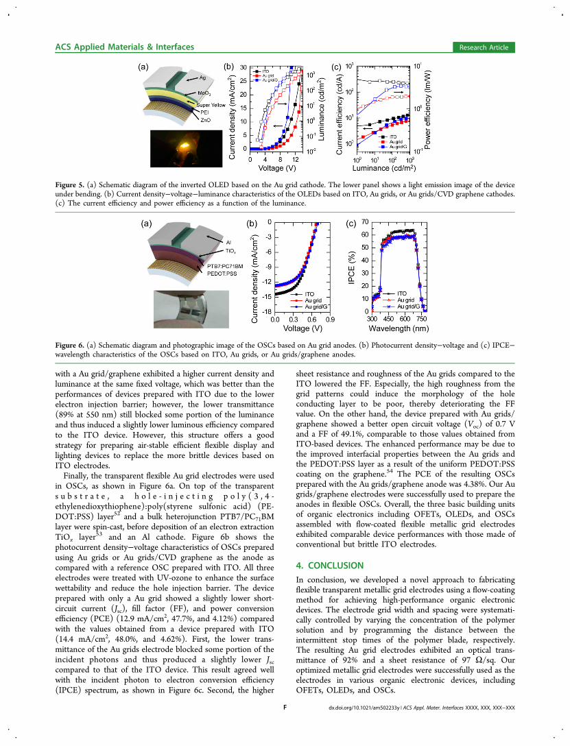
electrodes were fabricated. Compared with the pad-typeelectrodes, the utility of the grid electrode in an OFET yieldeda larger W/L ratio for a fixed area due to the comb-likegeometry. The ITO and cross-linked poly-4-vinylphenol(cPVP) were utilized as the gate electrode and gate dielectric,respectively. Source−drain electrodes were prepared bythermally depositing Au onto a cPVP surface through a shadowmask, followed by the aforementioned patterning steps (see theinset of Figure 4a). P-type pentacene was thermally depositedonto the channel region. Figure 4a shows the opticaltransmittance spectra of an OFET array fabricated on a PETsubstrate over the visible and near-infrared spectral range. Theoptical transmittance of a neat PET film was 89% at a
wavelength of 550 nm. The overall average transparency afterfabricating a pentacene FET array on PET was reduced toaround 76%. Parts b and c of Figure 4 show typical output andtransfer characteristics of the resulting devices, respectively. Thedevice exhibited reasonable gate modulation of ID in both thelinear and saturation regimes (Figure 4b). Our Au gridelectrodes resulted in good device performances with a nominalfield-effect mobility of 0.43 ± 0.09 cm2 V−1 s−1 (using L = 50μm and W = 1000 μm for calculation) and an on/off currentratio of ∼105.30 While the as-calculated mobility is anoverestimate value considering the comb-like geometry of theelectrodes (L must be shorter and W must be larger,effectively), it should be noted that that electrodes with largereffective W/L ratio are beneficial for generating higher currentlevel than those made in pad-type.The transparent flexible Au grid electrodes were next used in
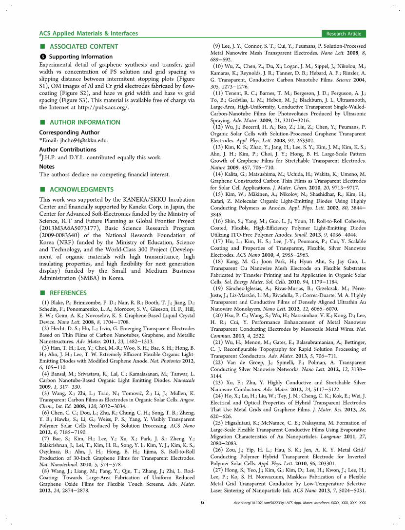
inverted OLEDs, as shown in Figure 5a. The basic architectureof the OLED consisted of five layers: an electron injecting ZnOlayer, an electron injecting polyethylenimine (PEI) interlayer,49
an emitting Super Yellow layer, a hole injecting MoO3 layer,and an Ag anode. Figure 5b shows the current density−voltage−luminance characteristics of the OLEDs preparedusing Au grids or Au grids/CVD graphene as the cathode. Theresults were compared with the properties of a reference OLEDprepared with ITO. The device having Au grids alone displayeda higher operating voltage, a lower current density, and a lowerluminous efficiency (8.69 cd/A and 1.96 lm/W) than the deviceprepared with ITO (13.5 cd/A and 5 lm/W). The largeelectron injection energy barrier from the Au grids (with a workfunction of ∼5.1 eV) to the ZnO (with a lowest unoccupiedmolecular orbital, LUMO, energy level of ∼4.4 eV) impededelectron injection and reduced the current density.50,51 A highersheet resistance was obtained from the Au grids (97 Ω/sq at92% at 550 nm) than from the ITO (12 Ω/sq at 90% at 550nm), which increased the operating voltage and reduced theluminance. On the other hand, the device prepared with Augrids/graphene showed a good current density, luminance, andluminous efficiency (10.1 cd/A and 3.42 lm/W). These valueswere comparable to those of ITO-based devices. The CVD-grown graphene was n-doped with PEI to reduce the electroninjection barrier.49 The improved performance of the deviceprepared with graphene (work function of ∼4.6 eV)convincingly demonstrated that a graphene interlayer couldeffectively reduce the electron injection barrier from thecathode to the electron injection layer, and thus increase theelectron injection into the emitting layer. The OLED prepared
Figure 3. (a) R/R0 for the ITO, Au film, and Au grid electrodes, as afunction of the strain level (±2.5%). The inset shows photographs ofthe Au grid electrode during compression and tension. (b) R/R0 as afunction of the cycling number during the 1% strain tension.
Figure 4. (a) UV−vis spectra of a PET substrate prepared with a pentacene FET array based on Au grid of source/drain electrodes. (b) Output and(c) transfer characteristics of the resulting transparent flexible pentacene FETs.
ACS Applied Materials & Interfaces Research Article
with a Au grid/graphene exhibited a higher current density andluminance at the same fixed voltage, which was better than theperformances of devices prepared with ITO due to the lowerelectron injection barrier; however, the lower transmittance(89% at 550 nm) still blocked some portion of the luminanceand thus induced a slightly lower luminous efficiency comparedto the ITO device. However, this structure offers a goodstrategy for preparing air-stable efficient flexible display andlighting devices to replace the more brittle devices based onITO electrodes.Finally, the transparent flexible Au grid electrodes were used
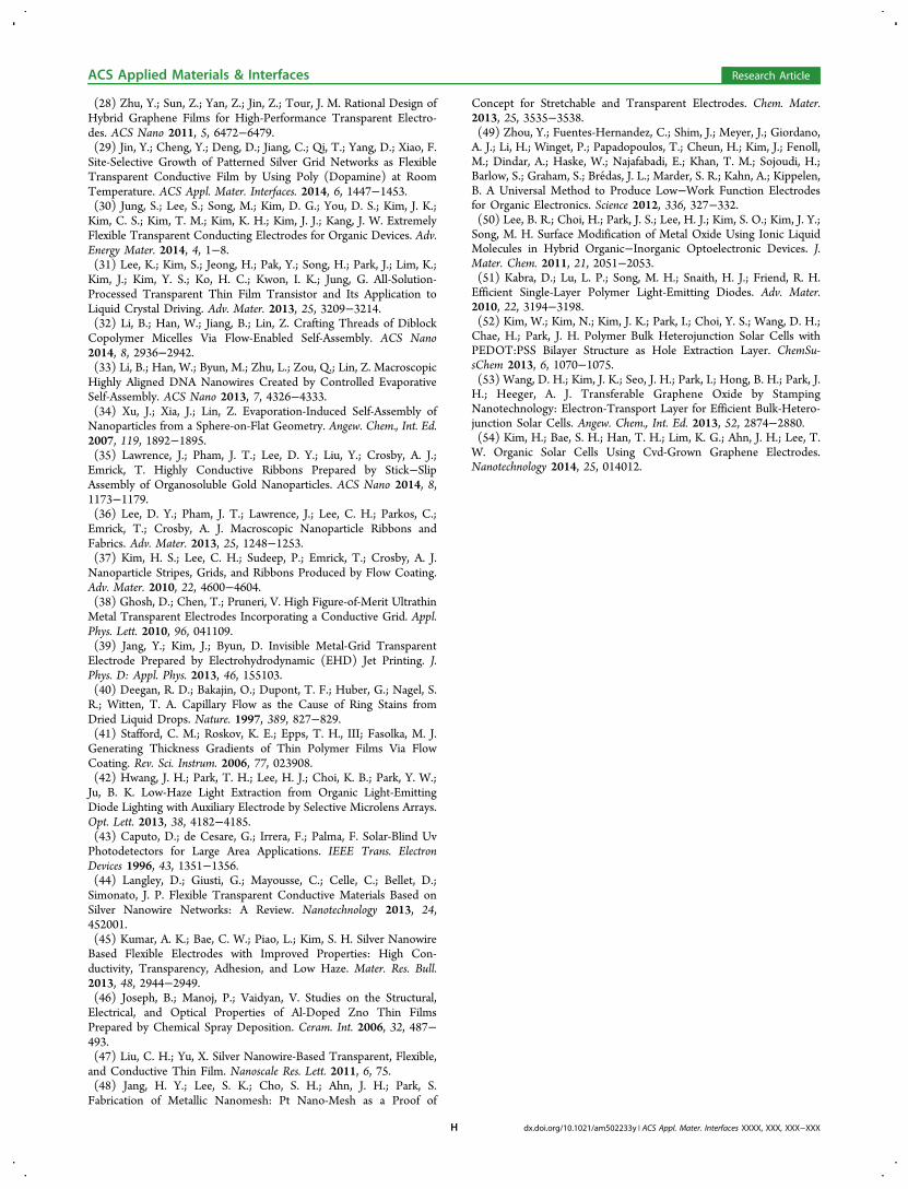
in OSCs, as shown in Figure 6a. On top of the transparents u b s t r a t e , a h o l e - i n j e c t i n g p o l y ( 3 , 4 -ethylenedioxythiophene):poly(styrene sulfonic acid) (PE-DOT:PSS) layer52 and a bulk heterojunction PTB7/PC71BMlayer were spin-cast, before deposition of an electron extractionTiOx layer53 and an Al cathode. Figure 6b shows thephotocurrent density−voltage characteristics of OSCs preparedusing Au grids or Au grids/CVD graphene as the anode ascompared with a reference OSC prepared with ITO. All threeelectrodes were treated with UV-ozone to enhance the surfacewettability and reduce the hole injection barrier. The deviceprepared with only a Au grid showed a slightly lower short-circuit current (Jsc), fill factor (FF), and power conversionefficiency (PCE) (12.9 mA/cm2, 47.7%, and 4.12%) comparedwith the values obtained from a device prepared with ITO(14.4 mA/cm2, 48.0%, and 4.62%). First, the lower trans-mittance of the Au grids electrode blocked some portion of theincident photons and thus produced a slightly lower Jsccompared to that of the ITO device. This result agreed wellwith the incident photon to electron conversion efficiency(IPCE) spectrum, as shown in Figure 6c. Second, the higher
sheet resistance and roughness of the Au grids compared to theITO lowered the FF. Especially, the high roughness from thegrid patterns could induce the morphology of the holeconducting layer to be poor, thereby deteriorating the FFvalue. On the other hand, the device prepared with Au grids/graphene showed a better open circuit voltage (Voc) of 0.7 Vand a FF of 49.1%, comparable to those values obtained fromITO-based devices. The enhanced performance may be due tothe improved interfacial properties between the Au grids andthe PEDOT:PSS layer as a result of the uniform PEDOT:PSScoating on the graphene.54 The PCE of the resulting OSCsprepared with the Au grids/graphene anode was 4.38%. Our Augrids/graphene electrodes were successfully used to prepare theanodes in flexible OSCs. Overall, the three basic building unitsof organic electronics including OFETs, OLEDs, and OSCsassembled with flow-coated flexible metallic grid electrodesexhibited comparable device performances with those made ofconventional but brittle ITO electrodes.
4. CONCLUSION
In conclusion, we developed a novel approach to fabricatingflexible transparent metallic grid electrodes using a flow-coatingmethod for achieving high-performance organic electronicdevices. The electrode grid width and spacing were systemati-cally controlled by varying the concentration of the polymersolution and by programming the distance between theintermittent stop times of the polymer blade, respectively.The resulting Au grid electrodes exhibited an optical trans-mittance of 92% and a sheet resistance of 97 Ω/sq. Ouroptimized metallic grid electrodes were successfully used as theelectrodes in various organic electronic devices, includingOFETs, OLEDs, and OSCs.
Figure 5. (a) Schematic diagram of the inverted OLED based on the Au grid cathode. The lower panel shows a light emission image of the deviceunder bending. (b) Current density−voltage−luminance characteristics of the OLEDs based on ITO, Au grids, or Au grids/CVD graphene cathodes.(c) The current efficiency and power efficiency as a function of the luminance.
Figure 6. (a) Schematic diagram and photographic image of the OSCs based on Au grid anodes. (b) Photocurrent density−voltage and (c) IPCE−wavelength characteristics of the OSCs based on ITO, Au grids, or Au grids/graphene anodes.
ACS Applied Materials & Interfaces Research Article
*S Supporting InformationExperimental detail of graphene synthesis and transfer, gridwidth vs concentration of PS solution and grid spacing vsslipping distance between intermitent stopping plots (FigureS1), OM images of Al and Cr grid electrodes fabricaed by flow-coating (Figure S2), and haze vs grid width and haze vs gridspacing (Figure S3). This material is available free of charge viathe Internet at http://pubs.acs.org/.
Author Contributions#J.H.P. and D.Y.L. contributed equally this work.
NotesThe authors declare no competing financial interest.
■ ACKNOWLEDGMENTS
This work was supported by the KANEKA/SKKU IncubationCenter and financially supported by Kaneka Corp. in Japan, theCenter for Advanced Soft-Electronics funded by the Ministry ofScience, ICT and Future Planning as Global Frontier Project(2013M3A6A5073177), Basic Science Research Program(2009-0083540) of the National Research Foundation ofKorea (NRF) funded by the Ministry of Education, Scienceand Technology, and the World-Class 300 Project (Develop-ment of organic materials with high transmittance, highinsulating properties, and high flexibility for next generationdisplay) funded by the Small and Medium BusinessAdministration (SMBA) in Korea.
■ REFERENCES(1) Blake, P.; Brimicombe, P. D.; Nair, R. R.; Booth, T. J.; Jiang, D.;Schedin, F.; Ponomarenko, L. A.; Morozov, S. V.; Gleeson, H. F.; Hill,E. W.; Geim, A. K.; Novoselov, K. S. Graphene-Based Liquid CrystalDevice. Nano Lett. 2008, 8, 1704−1708.(2) Hecht, D. S.; Hu, L.; Irvin, G. Emerging Transparent ElectrodesBased on Thin Films of Carbon Nanotubes, Graphene, and MetallicNanostructures. Adv. Mater. 2011, 23, 1482−1513.(3) Han, T. H.; Lee, Y.; Choi, M.-R.; Woo, S. H.; Bae, S. H.; Hong, B.H.; Ahn, J. H.; Lee, T. W. Extremely Efficient Flexible Organic Light-Emitting Diodes with Modified Graphene Anode. Nat. Photonics 2012,6, 105−110.(4) Bansal, M.; Srivastava, R.; Lal, C.; Kamalasanan, M.; Tanwar, L.Carbon Nanotube-Based Organic Light Emitting Diodes. Nanoscale2009, 1, 317−330.(5) Wang, X.; Zhi, L.; Tsao, N.; Tomovic, Z.; Li, J.; Mullen, K.Transparent Carbon Films as Electrodes in Organic Solar Cells. Angew.Chem., Int. Ed. 2008, 120, 3032−3034.(6) Chen, C. C.; Dou, L.; Zhu, R.; Chung, C. H.; Song, T. B.; Zheng,Y. B.; Hawks, S.; Li, G.; Weiss, P. S.; Yang, Y. Visibly TransparentPolymer Solar Cells Produced by Solution Processing. ACS Nano2012, 6, 7185−7190.(7) Bae, S.; Kim, H.; Lee, Y.; Xu, X.; Park, J. S.; Zheng, Y.;Balakrishnan, J.; Lei, T.; Kim, H. R.; Song, Y. I.; Kim, Y. J.; Kim, K. S.;Ozyilmaz, B.; Ahn, J. H.; Hong, B. H.; Iijima, S. Roll-to-RollProduction of 30-Inch Graphene Films for Transparent Electrodes.Nat. Nanotechnol. 2010, 5, 574−578.(8) Wang, J.; Liang, M.; Fang, Y.; Qiu, T.; Zhang, J.; Zhi, L. Rod-Coating: Towards Large-Area Fabrication of Uniform ReducedGraphene Oxide Films for Flexible Touch Screens. Adv. Mater.2012, 24, 2874−2878.
(9) Lee, J. Y.; Connor, S. T.; Cui, Y.; Peumans, P. Solution-ProcessedMetal Nanowire Mesh Transparent Electrodes. Nano Lett. 2008, 8,689−692.(10) Wu, Z.; Chen, Z.; Du, X.; Logan, J. M.; Sippel, J.; Nikolou, M.;Kamaras, K.; Reynolds, J. R.; Tanner, D. B.; Hebard, A. F.; Rinzler, A.G. Transparent, Conductive Carbon Nanotube Films. Science 2004,305, 1273−1276.(11) Tenent, R. C.; Barnes, T. M.; Bergeson, J. D.; Ferguson, A. J.;To, B.; Gedvilas, L. M.; Heben, M. J.; Blackburn, J. L. Ultrasmooth,Large-Area, High-Uniformity, Conductive Transparent Single-Walled-Carbon-Nanotube Films for Photovoltaics Produced by UltrasonicSpraying. Adv. Mater. 2009, 21, 3210−3216.(12) Wu, J.; Becerril, H. A.; Bao, Z.; Liu, Z.; Chen, Y.; Peumans, P.Organic Solar Cells with Solution-Processed Graphene TransparentElectrodes. Appl. Phys. Lett. 2008, 92, 263302.(13) Kim, K. S.; Zhao, Y.; Jang, H.; Lee, S. Y.; Kim, J. M.; Kim, K. S.;Ahn, J. H.; Kim, P.; Choi, J. Y.; Hong, B. H. Large-Scale PatternGrowth of Graphene Films for Stretchable Transparent Electrodes.Nature 2009, 457, 706−710.(14) Kalita, G.; Matsushima, M.; Uchida, H.; Wakita, K.; Umeno, M.Graphene Constructed Carbon Thin Films as Transparent Electrodesfor Solar Cell Applications. J. Mater. Chem. 2010, 20, 9713−9717.(15) Kim, W.; Makinen, A.; Nikolov, N.; Shashidhar, R.; Kim, H.;Kafafi, Z. Molecular Organic Light-Emitting Diodes Using HighlyConducting Polymers as Anodes. Appl. Phys. Lett. 2002, 80, 3844−3846.(16) Shin, S.; Yang, M.; Guo, L. J.; Youn, H. Roll-to-Roll Cohesive,Coated, Flexible, High-Efficiency Polymer Light-Emitting DiodesUtilizing ITO-Free Polymer Anodes. Small. 2013, 9, 4036−4044.(17) Hu, L.; Kim, H. S.; Lee, J.-Y.; Peumans, P.; Cui, Y. ScalableCoating and Properties of Transparent, Flexible, Silver NanowireElectrodes. ACS Nano 2010, 4, 2955−2963.(18) Kang, M. G.; Joon Park, H.; Hyun Ahn, S.; Jay Guo, L.Transparent Cu Nanowire Mesh Electrode on Flexible SubstratesFabricated by Transfer Printing and Its Application in Organic SolarCells. Sol. Energy Mater. Sol. Cells. 2010, 94, 1179−1184.(19) Sanchez-Iglesias, A.; Rivas-Murias, B.; Grzelczak, M.; Perez-Juste, J.; Liz-Marzan, L. M.; Rivadulla, F.; Correa-Duarte, M. A. HighlyTransparent and Conductive Films of Densely Aligned Ultrathin AuNanowire Monolayers. Nano Lett. 2012, 12, 6066−6070.(20) Hsu, P. C.; Wang, S.; Wu, H.; Narasimhan, V. K.; Kong, D.; Lee,H. R.; Cui, Y. Performance Enhancement of Metal NanowireTransparent Conducting Electrodes by Mesoscale Metal Wires. Nat.Commun. 2013, 4, 2522.(21) Wu, H.; Menon, M.; Gates, E.; Balasubramanian, A.; Bettinger,C. J. Reconfigurable Topography for Rapid Solution Processing ofTransparent Conductors. Adv. Mater. 2013, 5, 706−711.(22) Van de Groep, J.; Spinelli, P.; Polman, A. TransparentConducting Silver Nanowire Networks. Nano Lett. 2012, 12, 3138−3144.(23) Xu, F.; Zhu, Y. Highly Conductive and Stretchable SilverNanowire Conductors. Adv. Mater. 2012, 24, 5117−5122.(24) Ho, X.; Lu, H.; Liu, W.; Tey, J. N.; Cheng, C. K.; Kok, E.; Wei, J.Electrical and Optical Properties of Hybrid Transparent ElectrodesThat Use Metal Grids and Graphene Films. J. Mater. Res. 2013, 28,620−626.(25) Higashitani, K.; McNamee, C. E.; Nakayama, M. Formation ofLarge-Scale Flexible Transparent Conductive Films Using EvaporativeMigration Characteristics of Au Nanoparticles. Langmuir 2011, 27,2080−2083.(26) Zou, J.; Yip, H. L.; Hau, S. K.; Jen, A. K. Y. Metal Grid/Conducting Polymer Hybrid Transparent Electrode for InvertedPolymer Solar Cells. Appl. Phys. Lett. 2010, 96, 203301.(27) Hong, S.; Yeo, J.; Kim, G.; Kim, D.; Lee, H.; Kwon, J.; Lee, H.;Lee, P.; Ko, S. H. Nonvacuum, Maskless Fabrication of a FlexibleMetal Grid Transparent Conductor by Low-Temperature SelectiveLaser Sintering of Nanoparticle Ink. ACS Nano 2013, 7, 5024−5031.
ACS Applied Materials & Interfaces Research Article
(28) Zhu, Y.; Sun, Z.; Yan, Z.; Jin, Z.; Tour, J. M. Rational Design ofHybrid Graphene Films for High-Performance Transparent Electro-des. ACS Nano 2011, 5, 6472−6479.(29) Jin, Y.; Cheng, Y.; Deng, D.; Jiang, C.; Qi, T.; Yang, D.; Xiao, F.Site-Selective Growth of Patterned Silver Grid Networks as FlexibleTransparent Conductive Film by Using Poly (Dopamine) at RoomTemperature. ACS Appl. Mater. Interfaces. 2014, 6, 1447−1453.(30) Jung, S.; Lee, S.; Song, M.; Kim, D. G.; You, D. S.; Kim, J. K.;Kim, C. S.; Kim, T. M.; Kim, K. H.; Kim, J. J.; Kang, J. W. ExtremelyFlexible Transparent Conducting Electrodes for Organic Devices. Adv.Energy Mater. 2014, 4, 1−8.(31) Lee, K.; Kim, S.; Jeong, H.; Pak, Y.; Song, H.; Park, J.; Lim, K.;Kim, J.; Kim, Y. S.; Ko, H. C.; Kwon, I. K.; Jung, G. All-Solution-Processed Transparent Thin Film Transistor and Its Application toLiquid Crystal Driving. Adv. Mater. 2013, 25, 3209−3214.(32) Li, B.; Han, W.; Jiang, B.; Lin, Z. Crafting Threads of DiblockCopolymer Micelles Via Flow-Enabled Self-Assembly. ACS Nano2014, 8, 2936−2942.(33) Li, B.; Han, W.; Byun, M.; Zhu, L.; Zou, Q.; Lin, Z. MacroscopicHighly Aligned DNA Nanowires Created by Controlled EvaporativeSelf-Assembly. ACS Nano 2013, 7, 4326−4333.(34) Xu, J.; Xia, J.; Lin, Z. Evaporation-Induced Self-Assembly ofNanoparticles from a Sphere-on-Flat Geometry. Angew. Chem., Int. Ed.2007, 119, 1892−1895.(35) Lawrence, J.; Pham, J. T.; Lee, D. Y.; Liu, Y.; Crosby, A. J.;Emrick, T. Highly Conductive Ribbons Prepared by Stick−SlipAssembly of Organosoluble Gold Nanoparticles. ACS Nano 2014, 8,1173−1179.(36) Lee, D. Y.; Pham, J. T.; Lawrence, J.; Lee, C. H.; Parkos, C.;Emrick, T.; Crosby, A. J. Macroscopic Nanoparticle Ribbons andFabrics. Adv. Mater. 2013, 25, 1248−1253.(37) Kim, H. S.; Lee, C. H.; Sudeep, P.; Emrick, T.; Crosby, A. J.Nanoparticle Stripes, Grids, and Ribbons Produced by Flow Coating.Adv. Mater. 2010, 22, 4600−4604.(38) Ghosh, D.; Chen, T.; Pruneri, V. High Figure-of-Merit UltrathinMetal Transparent Electrodes Incorporating a Conductive Grid. Appl.Phys. Lett. 2010, 96, 041109.(39) Jang, Y.; Kim, J.; Byun, D. Invisible Metal-Grid TransparentElectrode Prepared by Electrohydrodynamic (EHD) Jet Printing. J.Phys. D: Appl. Phys. 2013, 46, 155103.(40) Deegan, R. D.; Bakajin, O.; Dupont, T. F.; Huber, G.; Nagel, S.R.; Witten, T. A. Capillary Flow as the Cause of Ring Stains fromDried Liquid Drops. Nature. 1997, 389, 827−829.(41) Stafford, C. M.; Roskov, K. E.; Epps, T. H., III; Fasolka, M. J.Generating Thickness Gradients of Thin Polymer Films Via FlowCoating. Rev. Sci. Instrum. 2006, 77, 023908.(42) Hwang, J. H.; Park, T. H.; Lee, H. J.; Choi, K. B.; Park, Y. W.;Ju, B. K. Low-Haze Light Extraction from Organic Light-EmittingDiode Lighting with Auxiliary Electrode by Selective Microlens Arrays.Opt. Lett. 2013, 38, 4182−4185.(43) Caputo, D.; de Cesare, G.; Irrera, F.; Palma, F. Solar-Blind UvPhotodetectors for Large Area Applications. IEEE Trans. ElectronDevices 1996, 43, 1351−1356.(44) Langley, D.; Giusti, G.; Mayousse, C.; Celle, C.; Bellet, D.;Simonato, J. P. Flexible Transparent Conductive Materials Based onSilver Nanowire Networks: A Review. Nanotechnology 2013, 24,452001.(45) Kumar, A. K.; Bae, C. W.; Piao, L.; Kim, S. H. Silver NanowireBased Flexible Electrodes with Improved Properties: High Con-ductivity, Transparency, Adhesion, and Low Haze. Mater. Res. Bull.2013, 48, 2944−2949.(46) Joseph, B.; Manoj, P.; Vaidyan, V. Studies on the Structural,Electrical, and Optical Properties of Al-Doped Zno Thin FilmsPrepared by Chemical Spray Deposition. Ceram. Int. 2006, 32, 487−493.(47) Liu, C. H.; Yu, X. Silver Nanowire-Based Transparent, Flexible,and Conductive Thin Film. Nanoscale Res. Lett. 2011, 6, 75.(48) Jang, H. Y.; Lee, S. K.; Cho, S. H.; Ahn, J. H.; Park, S.Fabrication of Metallic Nanomesh: Pt Nano-Mesh as a Proof of
Concept for Stretchable and Transparent Electrodes. Chem. Mater.2013, 25, 3535−3538.(49) Zhou, Y.; Fuentes-Hernandez, C.; Shim, J.; Meyer, J.; Giordano,A. J.; Li, H.; Winget, P.; Papadopoulos, T.; Cheun, H.; Kim, J.; Fenoll,M.; Dindar, A.; Haske, W.; Najafabadi, E.; Khan, T. M.; Sojoudi, H.;Barlow, S.; Graham, S.; Bredas, J. L.; Marder, S. R.; Kahn, A.; Kippelen,B. A Universal Method to Produce Low−Work Function Electrodesfor Organic Electronics. Science 2012, 336, 327−332.(50) Lee, B. R.; Choi, H.; Park, J. S.; Lee, H. J.; Kim, S. O.; Kim, J. Y.;Song, M. H. Surface Modification of Metal Oxide Using Ionic LiquidMolecules in Hybrid Organic−Inorganic Optoelectronic Devices. J.Mater. Chem. 2011, 21, 2051−2053.(51) Kabra, D.; Lu, L. P.; Song, M. H.; Snaith, H. J.; Friend, R. H.Efficient Single-Layer Polymer Light-Emitting Diodes. Adv. Mater.2010, 22, 3194−3198.(52) Kim, W.; Kim, N.; Kim, J. K.; Park, I.; Choi, Y. S.; Wang, D. H.;Chae, H.; Park, J. H. Polymer Bulk Heterojunction Solar Cells withPEDOT:PSS Bilayer Structure as Hole Extraction Layer. ChemSu-sChem 2013, 6, 1070−1075.(53) Wang, D. H.; Kim, J. K.; Seo, J. H.; Park, I.; Hong, B. H.; Park, J.H.; Heeger, A. J. Transferable Graphene Oxide by StampingNanotechnology: Electron-Transport Layer for Efficient Bulk-Hetero-junction Solar Cells. Angew. Chem., Int. Ed. 2013, 52, 2874−2880.(54) Kim, H.; Bae, S. H.; Han, T. H.; Lim, K. G.; Ahn, J. H.; Lee, T.W. Organic Solar Cells Using Cvd-Grown Graphene Electrodes.Nanotechnology 2014, 25, 014012.
ACS Applied Materials & Interfaces Research Article