20
1/20 FoCal-E pad readout Olivier Bourrion CNRS/IN2P3/LPSC 30 th march 2021
1/20
FoCal-E pad readout
Olivier BourrionCNRS/IN2P3/LPSC
30th march 2021

2/20
Outline● System overview● Review of each electronic part● Demonstrator● Summary

3/20
Detector overview and front-end
● Each cell will be equipped with a SiPad of 72 pixels● Each SiPad will be read-out with an HGCROC ASIC● 18 of the 20 layers will use SiPad, that is :
– 18*11*2=396 five-pad-layer boards– 1980 HGCROC V2 ASICs– 142,560 channels
11 modules
20 layers
(18 SiPad+ 2 m
aps)
Width of 2x 5 cells
One 5-pad-layer board
See N. N
ovitzk
y’s prese
ntation
(29/03 @ 10am)

4/20
Reading the pad-layers
● Aggregator :– host the FPGA that reads out the
HGCROC – Communicates with the Common Readout
Unit (CRU) through an optical fiber– Optionally communicate with a SUM-
board for self-trigger (see next slide)
● 5 aggregators + interface board per tower– 5*11*2=110 boards required– 5 CRUs with 24 optical links required to
readout the whole detector
Interface board « Final »
Aggregator Board for 4 layers
MAPs layer
5-Pad Layer board
BEAM direction
Last aggregator board for 2 layers only
Vertical stacking allows for coincidences searches between layers at the aggregator stage

5/20
Trigger option
● Energy deposit higher at mid-depth => better sensitivity for a trigger– => If we were to consider to possibility to self trigger, we should limit the trigger
input to the aggregators sitting at mid-depth.
● 22 inputs to a dedicated SUM board– => difficulty here : guarantee a constant latency between any physic interaction
and candidate trigger (tuning!)
● The SUM board would communicate with CTP through a single connection
Interaction is far from detectorArrival angle is ~ perpendicular
interaction
FOCAL
Interaction is far from detectorArrival angle is ~ perpendicular
Interacting particle
What happens in one tower
aggregators
SUMBOARD22 inputs
« Crown » of candidate at mid-depth => 22 sources
To Central Trigger Processor
Are
as a
bove
thre sh
olds
Decision = OR, multiplicity
One aggregator only per tower

6/20
Electronics architecture in summary
● 396 five-pad-layer boards● 110 aggregators● 110 interface boards● 1 sum board ?
SUMBOARD
aggregator
Inte
rfac
ebo
ard
5-pad-layer board
5-pad-layer board5-pad-layer board
5-pad-layer board
4 times
aggregator
Inte
rfac
ebo
ard
5-pad-layer board
5-pad-layer board
1 time
11 times
2 times (one per side)5 CRU boards
(in 2 or 3 FLPs)
22 fibers
CTP
DAQ
110 fibers
Trigger candidate
10G-PON network
Trigger decisions and messages
11 modules
Width of 2x 5 cells
Interface board « Final »
Aggregator Board for 4 layers
MAPs layer
5-Pad Layer board
BEAM direction
Last aggregator board for 2 layers only

7/20
Outline● System overview● Review of each electronic part● Demonstrator● Summary
8/20
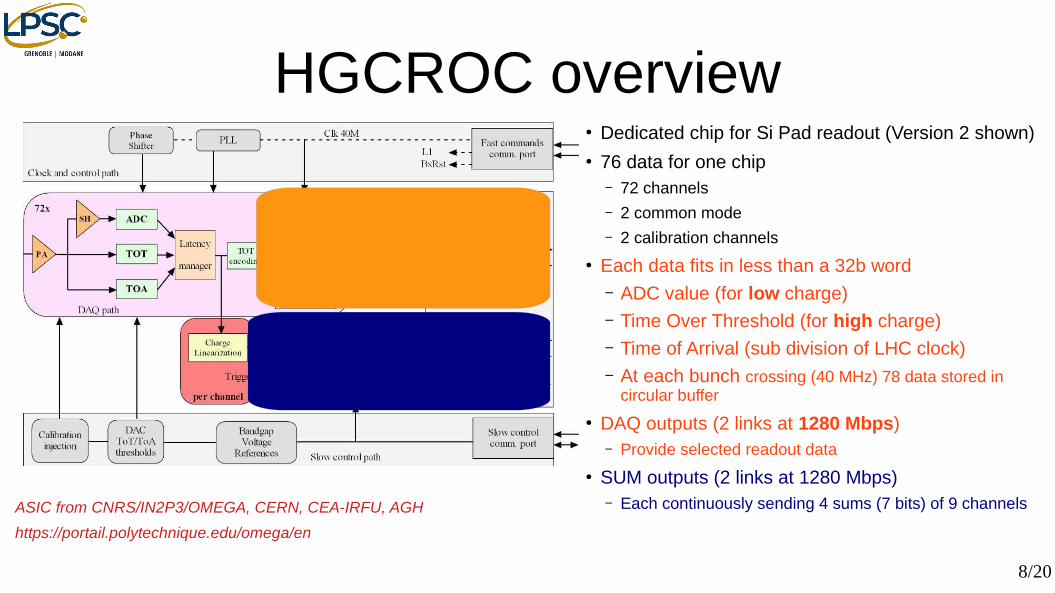
HGCROC overview● Dedicated chip for Si Pad readout (Version 2 shown)● 76 data for one chip
– 72 channels– 2 common mode– 2 calibration channels
● Each data fits in less than a 32b word– ADC value (for low charge)– Time Over Threshold (for high charge)– Time of Arrival (sub division of LHC clock)– At each bunch crossing (40 MHz) 78 data stored in
circular buffer
● DAQ outputs (2 links at 1280 Mbps)– Provide selected readout data
● SUM outputs (2 links at 1280 Mbps)– Each continuously sending 4 sums (7 bits) of 9 channels ASIC from CNRS/IN2P3/OMEGA, CERN, CEA-IRFU, AGH
https://portail.polytechnique.edu/omega/en

9/20
Channel/sum mapping● 72 channels
– Upon readout command via the DAQ links
● 8 SUM regions of 9 pixels– Continuously via the SUM links
1 3 2 0 8 36 38 39 37
5 7 6 4 44 40 42 43 41
9 11 10 12 48 50 46 47 45
17 13 15 14 16 52 51 49 53
18 20 21 19 23 55 57 56 54
26 22 24 25 59 61 60 58 62
30 28 29 27 67 63 65 64 66
34 32 33 31 35 71 69 68 70
Reading-out 1376b at 1280Mbps takes 1.075 µs (≈930kHz)

10/20
Challenges around the 5-pad-layer board
● Radiations– Use qualified components
● Limited available height (8.5mm)– Impact on the cooling strategy (copper plate)– Connector pitch on interface boards !
● One side with no components● Holes and cavities for bounding the Si Pad● Heat dissipation (~10W per 5-pad-layer)● Validation before mounting
– Test PCB before bounding Si Pads
Tungsten plate
Si-PAD sensor (t=0.32 [mm])
Spacerbar
HGCROC (t=1.2 [mm])
Power supply(t=2.82 [mm])
FPC Connector t=2 [mm]
3.5 mm
Up to5 mm
8 mm
BGA Front-End Wire bonding Adhesive sheets
Spacerbar
PCB PAD-1 (t = 1.3 [mm])
Glue PaddingRadhard comp.
Power Supply D
Power Supply A
Power Supply D
Power Supply A
Power Supply D
Power Supply A
Power Supply D
Power Supply A
Power Supply D
Power Supply A
1
HGCROC
Probes Probes Probes Probes Probes
HGCROCHGCROCHGCROCHGCROC
8 cm
9 cm
45 cmTop view (from the beam)
Side view (from the detector left and right)

11/20
Toward 5-pad-layer, gaining experience● Single-pad board
– designed with final dielectric material– actual PCB thickness – holes positioning and cavities were inserted
=> compatible with bounding machine
● A dedicated interface board (single-pad ↔ KCU105) was designed

12/20
Single pad board test setup
Single pad board connected to the KCU105 via the test interface board

13/20
Mechanical issue found● Constraints related to
bounding were to stringent (mechanical constraints with large cavities)
● Some mistakes in the PCB (design and production)
New design with● Smaller cavity● Larger thickness (1.6mm instead of
1.3mm● Smaller holes and cavity
15.4
mm
3.1
mm
4 m
m
5 mm
4.35
mm
5 m
m
9 mm
4 m
m4.
5 m
m5.
2 m
m
New proposal: all components are on TOP and small cavity for wire bonding
CMS Res. 1206
« TOP »
Inner Layer
CMS Cap. 1206
Non-plated Hole
0.5mm square contactENEPIG PCB Finishes
Pad connection position

14/20
Challenges around the interface board● Vertical stacking to allow
trigger option● Limited height for
connectors (8.5 mm pitch )– Large number of signals– Critical signals (supplies,
serial lines, high voltage)
● Keep an access for cooling– 5-pad-layer will stick-out a
bit from the detector to make room for cold reference
Interface board « Final »
Aggregator Board for 4 layers
MAPs layer
5-Pad Layer board
BEAM direction
Last aggregator board for 2 layers only
Connector(to interface PCB)
HGCROC (1,2mm)
Si-PAD (0,32mm)Adhesive sheet (0,1mm)Tungsten plate (3,5mm)
PCB (1,3mm)
Cooling copper plate (1,7mm)
8,5
mm
Cooling fluid
5-pad layer
Connector :● Dark gray : SAMTEC ERM8-070-01-L-D-RA● Dark blue : SAMTEC ERF8-070-05.0-L-DV● Dark red : 2x SAMTEC SEAM8-30-S02.0-L-10-2● Orange : 2x SAMTEC SEAF8-30-1-L-10-2-RA
interface
Agregator

15/20
Aggregator overview5-pad layer
interface
Agregator
FPGA<25 W
SFP GBT_DAQ
4 S
MA
(cop
per
trig
)
SFP GBT_SPA
SFP ETH
SFP OPT_TRIG
PWR
4x8.5mm
80
mm
Unknown yet (probably more than 100 mm)
SFP :● Width : 14 mm● Length : 50 mm
12V @ 6.5A1kV for polarizationHV
xVDD_rawPOWER
xVDD_rawPOWER
POWERS
POWERS
POWERS
SFP = 50 mmFPGA = 35 mm
● Interfaces – 4 pads layers per aggregator)
● 80 differential pairs @1280Mbps in input● 40 differential pairs @320Mbps in output
– Up to 2 GBT links (future use)– One SFP cage for Ethernet (1G, 10G either optical or copper)– Triggers in/out : copper and optical
● GBT link– Allows machine clock recovery
(40.08MHz)– Upstream : for DAQ (expected mean
rate 1.89Gb/s => fit in one GBT link)– Downstream : for trigger messages

16/20
Injector board overview● Tool
– for characterizing the pad-layers (single and five)
– Production testing (before SiPad bonding)
● Signal injected on capacitor pads with spring contacts from the top side– Mechanical structure needed too manage
loading and positioning– 72 contacts => 28 Newtons
● Can inject on any pattern of pixels● Within each SUM group (9 pixels), bias
can tuned independently● Controlled either by the KCU105 or the
aggregator– External clock input for synchronicity with
HGCROC clock– Trigger input
XC7A35T-2FGG484
SYSCLK50
POWERS
TRIG_OUT_copperLVCMOS33
DAC0 (SPI bus)
serial_flash(s25FL256SAGNFI001)
TRIG_IN
LVCMOS33 com
p TRIG_IN_SMA
VTH1_COMP
GATE_P x74 (diff)72 channels
2 calibrations
DAC1 (SPI bus)
AD5668(8 channels DAC)
VB(4..0)VTH1_comp
VB(10..5)VTH2_comp
ETH PHY(88E1111)
CLK125
RJ45
AD5668(8 channels DAC)
GROUP0VB(8..0)
GATE_P(08..00)
GROUP1VB(8..0)
GATE_P(17..09)
GROUP2VB(8..0)
GATE_P(26..18)
GROUP3VB(8..0)
GATE_P(35..27)
GROUP4VB(8..0)
GATE_P(44..36)
GROUP5VB(8..0)
GATE_P(53..45)
GROUP6VB(8..0)
GATE_P(62..54)
GROUP7VB(8..0)
GATE_P(71..63)
CALIB0VB(9)
GATE_P(72)
CALIB1VB(10)
GATE_P(73)
Front-end
Each group contains 9
pixels, each with a different
bias
JTAG
CLK40_IN
LVCMOS33 com
p CLOCK_IN_SMA
VTH2_COMP
0.39N per pin
https://cdn.harwin.com/pdfs/P70-600.pdf
1 3 2 0 8 36 38 39 37
5 7 6 4 44 40 42 43 41
9 11 10 12 48 50 46 47 45
17 13 15 14 16 52 51 49 53
18 20 21 19 23 55 57 56 54
26 22 24 25 59 61 60 58 62
30 28 29 27 67 63 65 64 66
34 32 33 31 35 71 69 68 70

17/20
Outline● System overview● Review of each electronic part● Demonstrator● Summary
18/20
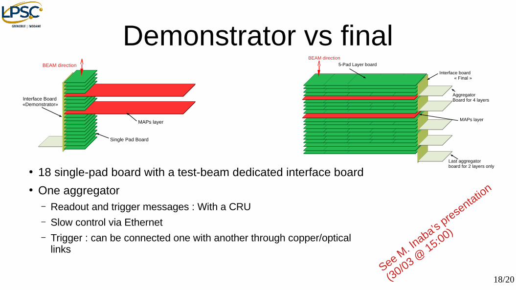
Demonstrator vs final
● 18 single-pad board with a test-beam dedicated interface board ● One aggregator
– Readout and trigger messages : With a CRU – Slow control via Ethernet– Trigger : can be connected one with another through copper/optical
links
Interface board « Final »
Aggregator Board for 4 layers
MAPs layer
5-Pad Layer board
BEAM direction
Last aggregator board for 2 layers only
Interface Board «Demonstrator»
Single Pad Board
MAPs layer
BEAM direction
See M. In
aba’s prese
ntation
(30/03 @ 15:00)

19/20
Outline● System overview● Review of each electronic part● Demonstrator● Summary

20/20
Summary of our progress and plans● Single-pad-board
– Qualify functionally the current design– PCB redesign in progress– A lot of interactions with mechanics for best integration
● Injector board– Firmware ready– In cabling
● Aggregator– In layout (part placed)– Power Distribution Network routed and simulated– Firmware will reuse many parts from KCU105 test bed, need to add CRU interface (trigger and DAQ)
● Demonstrator interface board– Layout to start right after aggregator is shipped to fabrication


