Page 1
Folded Waveguide Resonator Filter for
Communication and Radar Systems
Sultan K. Alotaibi
A dissertation submitted for the degree of Doctor of Philosophy
Heriot-Watt University
School of Engineering and Physical Sciences
April 2009
This copy of the thesis has been supplied on condition that anyone who consults it is
understood to recognise that the copyright rests with its author and that no quotation
from the thesis and no information derived from it may be published without the prior
written consent of the author or of the University (as may be appropriate).
Page 2
I
Abstract
In this thesis, a primary investigation into developing a compact and low-loss bandpass
filter, using novel folded waveguide resonators with a footprint reduction, has been
addressed. A slot coupling between adjacent resonators is introduced, which is
characterized by using full-wave EM simulations and verified experimentally. Two
designs of 2-pole folded waveguide resonator filters of this type have been considered,
fabricated and tested. In this thesis, an even more compact FWG resonator filter using a
novel slot technique is reported. The attainable size reduction is about 50%, and the
filter design is based on theoretical and full-wave electromagnetic (EM) simulations.
Based on FWG structure, two types of folded waveguide resonators have been studied
and considered the half-wavelength resonator and the quarter-wavelength resonator.
Moreover, both structures for the realization of microwave cavities with high-Q, with
the result of a high spurious free range and reduced footprint, have been evaluated.
Furthermore, a novel folded waveguide resonator with about a 75 % reduction of the
volume from the conventional size has been described. For comparison, two types of
folded waveguide resonators have been studied, i.e. the quarter-wavelength resonator of
square shape and the newly proposed triangular shape. In addition, a demonstration of a
filter application for miniature triangular folded waveguide resonators has been
designed and simulated using an EM simulator.
In addition, numbers of experiments have been conducted to develop cavity FWG and
Substrate Integrated folded waveguide SIFW resonator filters using a folded structure,
which is the main aim of this thesis. Furthermore, this thesis deals with the simulation
and implementation for many designs and topologies of FWG and SIFW resonator
filters and their frequency response. Simulation and experimental results were presented
to validate the design and to show the advantages of these types of filters. In addition, a
new type of filter with a compact multi-layer structure and low loss is attractive for
implementation with advanced device technologies, such as micromachining, LTCC
and LCP technologies.
Page 3
II
Dedication
To
My father Khalid for his love, encouragement and patience.
My mother, Mariam, for her love, support and sacrifice. She continues to
be a source of inspiration to me throughout my life.
My sisters and brothers, who are always there to offer a moment of clarity.
&
I must keep special thanks for my wife Badriah and my children Moath,
Omar and Maraim for their support and unconditional love, without which
I would never have completed this work.
Page 4
III
Acknowledgements
I would like to express my gratitude for the guidance provided by my supervisor Dr Jia-
Sheng Hong and for his excellent supervision, concern and endless support from the first
day. He has always been a great source of encouragement. Throughout my doctoral work,
he has kept me motivated and given me guidance to develop my research skills.
I would also like to thank Dr. Young-Hoon Chun who gave assistance in compiling the
test set-up with instructions on the operation of the equipment.
Special thanks go to Dr. Farid Almalol, Dr. Srikanth Lavu, Dr. Hazem Fayad and all
the Microwave Research Group at Heriot-Watt University for their support,
encouragement and assistance along the way.
I would like to extend my gratitude to the mechanical workshop staff, who have been
prompt in helping me with my PhD. Thanks are also due to all friends who have
encouraged me during my studying, and special thanks are given to Dr. Fasial AL-Shrif,
Dr. Abdullrahman Bagais, Dr. Abdullrahman Alghamdi who assisted and supported me
along the way.
I am grateful for the funding provided for my studies by the Saudi Interior Ministry,
represented by the Border Guard, as well as the support from Heriot-Watt University.
Most of all, I thank ALLAH for giving me everything.
Sultan K. AL-otaibi.
Page 5
IV
ACADEMIC REGISTRY
Research Thesis Submission
Name: Sultan K. Alotaibi
School/PGI: School of Engineering and Physical Sciences/Electrical
Electronics and Computer Department
Version: (i.e. First,
Resubmission, Final) Final Degree Sought: PhD
Declaration
In accordance with the appropriate regulations I hereby submit my thesis and I declare that:
1) the thesis embodies the results of my own work and has been composed by myself
2) where appropriate, I have made acknowledgement of the work of others and have made reference
to work carried out in collaboration with other persons
3) the thesis is the correct version of the thesis for submission and is the same version as any
electronic versions submitted*.
4) my thesis for the award referred to, deposited in the Heriot-Watt University Library, should be
made available for loan or photocopying and be available via the Institutional Repository, subject
to such conditions as the Librarian may require
5) I understand that as a student of the University I am required to abide by the Regulations of the
University and to conform to its discipline.
* Please note that it is the responsibility of the candidate to ensure that the correct version of the
thesis is submitted.
Signature of
Candidate:
Date:
Submission
Submitted By (name in capitals):
Page 6
V
Signature of Individual Submitting:
Date Submitted:
For Completion in Academic Registry
Received in the Academic Registry
by (name in capitals):
1.1 Method of Submission
(Handed in to Academic Registry; posted
through internal/external mail):
1.2 E-thesis Submitted
Signature:
Date:
Page 7
VI
Table of Contents
ABSTRACT..................................................................................................................... I
DEDICATION................................................................................................................II
ACKNOWLEDGEMENTS......................................................................................... III
TABLE OF CONTENTS............................................................................................. VI
LISTS OF FIGURES .....................................................................................................X
LISTS OF TABLES .................................................................................................... XV
GLOSSARY................................................................................................................XVI
LIST OF PUBLICATIONS BY THE CANDIDATE ......................................... XVIII
CHAPTER 1 ....................................................................................................................1
1.1 Motivations ..........................................................................................................1
1.2 Aims and Objective .............................................................................................2
1.3 Thesis structure guide ..........................................................................................2
CHAPTER 2 ....................................................................................................................5
2.1 Introduction: ........................................................................................................5
2.2 Microwave filter’s history: ..................................................................................6
2.3 Filter Classification:.............................................................................................8
2.4 Filter parameters:-................................................................................................9
2.5 RF and microwave resonators: ..........................................................................10
2.5.1 RF Resonator:- ............................................................................................10
2.5.1.1 Cavity Shapes ..........................................................................................11
2.5.1.2 Rectangular cavity: ..................................................................................11
2.5.1.3 A cylindrical cavity: ................................................................................12
2.5.1.4 Other cavity shapes:.................................................................................13
2.5.1.5 Microstrip resonator:- ..............................................................................13
Page 8
VII
2.5.1.6 Dielectric resonators: ...............................................................................13
2.6 Cavity Resonators ..............................................................................................15
2.6.1 Advantages of the cavity resonator:-...........................................................16
2.6.2 Resonant frequency of the cavity................................................................16
2.6.3 Quality Factor of the cavity resonator:........................................................17
2.6.4 Tuning of the cavity resonator: ...................................................................19
2.7 Rectangular cavity & Modelling of FWG resonator: ........................................21
2.7.1 Folded waveguide resonator concept ..........................................................24
2.7.2 Novel Realizations of FWG resonator. .......................................................26
2.7.3 Experimental Demonstration of FWG resonator. .......................................27
2.7.4 Folded waveguide FWG resonator filter:....................................................29
2.7.5 Folded waveguide FWG and coupling method: .........................................30
2.8 Substrate Integrated Waveguide SIFW Filter....................................................31
2.8.1 Microstrip Filters with Cross-Couplings: ...................................................32
2.9 Dual-Band Filter ................................................................................................34
2.10 Summary............................................................................................................35
CHAPTER 3 ..................................................................................................................36
3.1 Introduction: ......................................................................................................36
3.2 Design method ...................................................................................................36
3.2.1 Periodic Structures: .....................................................................................36
3.2.2 Image Parameter Method: ...........................................................................37
3.2.3 Insertion Loss Method ................................................................................37
3.2.3.1 Low-pass Prototype Filters: .....................................................................38
3.2.3.2 Low-pass Converted to a Bandpass:- ......................................................39
3.3 Summary............................................................................................................40
CHAPTER 4 ..................................................................................................................40
4.1 Introduction........................................................................................................41
4.2 Miniature Folded Waveguide FWG Resonators Realization ............................41
4.3 Fabrication and Experimental Results of Miniature FWG ...............................44
4.4 Filter Realization and Simulation of Miniature FWG Resonator ......................47
4.5 Summary............................................................................................................49
Page 9
VIII
CHAPTER 5 ..................................................................................................................50
5.1 Introduction........................................................................................................50
5.2 FWG FILTER USING A SLOT TECHNIQUE .............................................................51
5.2.1 Theoretical analysis.....................................................................................52
5.2.1.1 TZ from the High side: ............................................................................53
5.2.1.2 TZ from the Low side: .............................................................................54
5.2.2 Modelling of the FWG filter using a slot technique ...................................55
5.2.2.1 Design and modelling of the FWG filter using a slot technique: ............56
5.2.2.2 Design (1) TZ in the high side band ........................................................57
5.2.2.3 Design (2) TZ from low side band ..........................................................58
5.2.3 Fabrication of the filter ...............................................................................59
5.2.3.1 Implementation of a 2-pole cavity resonator filter: .................................60
5.2.3.2 Experiment Results ..................................................................................62
5.3 FWG Dual-band filter........................................................................................65
5.3.1 External and unloaded quality factor and coupling coefficients.................66
5.3.1.1 External Quality factor (Qe) ....................................................................66
5.3.1.2 Unloaded Quality factor (Qu) ..................................................................68
5.3.1.3 Coupling coefficient ................................................................................69
5.3.2 Dual-band operation Demonstration ...........................................................78
5.3.3 4-pole multilayer substrate integrated SIFW dual-band filter.....................82
5.4 Summary............................................................................................................83
CHAPTER 6 ..................................................................................................................84
6.1 Introduction........................................................................................................84
6.2 Novel coupled folded waveguide (FWG) resonator filter .................................85
6.2.1 1-pole resonator:..........................................................................................87
6.2.2 2-pole and 4-pole resonator filters: .............................................................88
6.2.2.1 Approach of extracting the coupling coefficient (K)...............................89
6.2.2.2 Extracting the coupling coefficient (K) ...................................................91
6.2.3 Simulation results for coupling coefficients (K).........................................93
6.2.3.2 Conclusions from the simulation results K12, K34 and K23 ......................96
6.3 Implementation of a 4-pole cavity resonator (Design 1): ..................................97
6.3.1 Verification approach..................................................................................99
6.3.2 Results:......................................................................................................100
Page 10
IX
6.4 Implementation of a 4-Pole cavity resonator (Design 2):................................102
6.4.1 Filter Design..............................................................................................102
6.4.1.1 Extracting external quality factor (Qe) ..................................................104
6.4.1.2 Extracting coupling coefficients ............................................................106
6.4.1.3 Filter demonstration...............................................................................109
6.5 Summary:.........................................................................................................113
CHAPTER 7 ................................................................................................................114
7.1 Introduction......................................................................................................114
7.2 SIFW resonators filter (Design 1): ..................................................................115
7.2.1 Cavity Size ................................................................................................116
7.2.2 1- pole SIFW resonator .............................................................................116
7.2.3 Simulation results of the single SIFW resonator: .....................................117
7.2.3.1 Diameter of via d at 0.2 mm .................................................................117
7.2.3.2 Diameter of via d at 0.5 mm ..................................................................118
7.2.3.3 Diameter of via d at 0.8 mm ..................................................................119
7.2.4 2-Pole of SIFW resonator .........................................................................120
7.2.4.1 Simulated loss effects in SIFW..............................................................121
7.2.5 Demonstration of the (SIFW) resonator filter (Design 1):........................124
7.3 A substrate integrated folded waveguide (SIFW) resonator filter (Design 2): 128
7.3.1 Demonstration of the (SIFW) resonator filter (Design 2):........................129
7.4 Summary..........................................................................................................133
CHAPTER 8 ................................................................................................................135
8.1 Introduction: ....................................................................................................135
8.2 Progress of the work ........................................................................................135
8.3 Contributions of the thesis ...............................................................................137
8.4 Suggestions for Further Work .........................................................................139
APPENDIX A ..............................................................................................................141
APPENDIX B ..............................................................................................................163
REFERENCE:.............................................................................................................168
Page 11
X
Lists of Figures
Figure 2-1: Frequency allocations ....................................................................................5
Figure 2-2: The response of an ideal filter . ......................................................................9
Figure 2-3: Typical resonant circuit; (a) series and (b) shunt resonator. ........................10
Figure 2-4 Rectangular Cavity Resonator.......................................................................11
Figure 2-5: Rectangular waveguide cavity resonator .....................................................12
Figure 2-6: Development of a cylindrical resonant cavity..............................................12
Figure 2-7: Several types of cavities...............................................................................13
Figure 2-8: Fundamental mode fields for three dielectric-resonator configurations. .....14
Figure 2-9: Rectangular cavity resonator........................................................................17
Figure 2-10: Conventional TE101 waveguide resonator with standing waves. ...............17
Figure 2-11: Cavity tuning by volume . ..........................................................................20
Figure 2-12: Methods of changing the resonant frequency of a cavity...........................21
Figure 2-13: Methods of changing the resonant frequency of a cavity...........................21
Figure 2-14: Rectangular Waveguide Resonator.. .........................................................22
Figure 2-15: A Schematic view of the folded waveguide resonator...............................23
Figure 2-16: Conventional TE 101 waveguide resonator ..............................................25
Figure 2-17: Folded waveguide half-wavelength resonator ...........................................26
Figure 2-18: FWG quarter-wavelength resonator with standing waves resonator . .......26
Figure 2-19: Realization and Standing wave pattern of FWG quarter- wavelength.......27
Figure 2-20: The distribution of field for the FWG cavity.(a) mode 1 and (b)mode 2...27
Figure 2-21: Simulated and Measured resonant frequency response..............................28
Figure 2-22: Fabricated filter before and after assembly. ...............................................29
Figure 2-23: 3-D model of 2-pole coupled folded waveguide resonator filter . ............30
Figure 2-24: Measured performance of the fabricated 2-pole folded waveguide . .........30
Figure 2-25: A 4th order folded waveguide filter with a cross-coupling........................31
Figure 2-26: Some cross-coupled planar microwave bandpass filters comprised ..........33
Figure 2-27: Mixed coupling structure . ........................................................................33
Figure 2-28: Typical resonant mode splitting phenomena of a mixed-coupled..............34
Figure 3-1: Periodic diaphragms in a waveguide............................................................37
Figure 3-2: A block diagram showing the steps of filter design. ....................................38
Figure 3-3: Elements of the low-pass prototype filter . ..................................................39
Figure 4-1: Square and Triangular FWG quarter-wavelength resonator. ......................42
Figure 4-2 Field distribution of the square and triangular FWG quarter-wavelength ....44
Page 12
XI
Figure 4-3 A fabricated single square FWG resonator before and after assembly. ........45
Figure 4-4 A fabricated single triangular FWG resonator before and after assembly ..45
Figure 4-5 Measured resonant frequency response of the FWG resonator....................47
Figure 4-6: Measured wideband frequency response of the fabricated FWG. ...............47
Figure 4-7 3D model of a 2-pole filter with coupled triangular FWG resonators. ........48
Figure 4-8. Simulated frequency response of the coupled triangular FWG resonators. 48
Figure 4-9 Performance of the compact and low-loss filter using miniature FWG........49
Figure 5-1 :Configuration and Coupling of a 2-pole FWG resonator filter....................51
Figure 5-2: Theoretical Responses of the filter with TZ in the High side band..............53
Figure 5-3: Phase Response of the filter with TZ in the High side band. .......................54
Figure 5-4: Theoretical Responses of the filter with TZ in the Low side band. .............54
Figure 5-5: Phase Response of the filter with TZ in the Low side band.........................55
Figure 5-6: Layout for bandpass filter design (a) Side View, (b) top View. ..................56
Figure 5-7 1-pole resonator filter. ...................................................................................57
Figure 5-8: Frequency response for a 1-pole resonator. .................................................57
Figure 5-9: Layout of 2-pole resonator filter with TZ in the high side band . ...............58
Figure 5-10 : The response of the best design of a 2-pole resonator filter......................58
Figure 5-11: Layout of 2-pole resonator filter with TZ in the low side band. ...............59
Figure 5-12: The responses of 2-pole resonator filter with TZ in the low side. ............59
Figure 5-13: 2-pole cavity resonator filter. .....................................................................60
Figure 5-14: Coupling characteristics against the slot length SL . .................................61
Figure 5-15:Fabricated 2-pole slotted FWG resonator filter before and after assembly.62
Figure 5-16: Frequency response of 2-pole FWG resonator filter with a TZ (Low) ......63
Figure 5-17: Frequency response of 2-pole FWG resonator filter with a TZ.(High) .....63
Figure 5-18:Wideband frequency response of fabricated 2-pole FWG (TZ high side)..64
Figure 5-19: Wideband frequency response of fabricated 2-pole FWG (TZ Low side). 64
Figure 5-20: Proposed FWG dual-band filter structure. ................................................65
Figure 5-21: Coupling scheme for the proposed dual-band filter. .................................66
Figure 5-22: The proposed technique to extract quality factor .......................................67
Figure 5-23: Design curves to extract the external quality factor. ..................................68
Figure 5-24: Resonant frequency characteristics of the scattering parameters...............69
Figure 5-25: Dual-band frequency characteristic against the couplings K12 and K34 for
the other parameters fixed. (a) K12 = K34 = 2.0. (b) K12 = K34 = 1.3. ............................70
Figure 5-26:Dual-band frequency characteristic against the couplings for K12 and K34
fixed. (a)Ks1=K3L=1.05 and K23=K14=0.6. (b)Ks1=K3L=0.75 and K23=K14= 0.3. ...........71
Page 13
XII
Figure 5-27: Configuration of dual passband filter to extract the direct coupling..........72
Figure 5-28: Typical frequency response simulated for extracting the coupling............73
Figure 5-29: Design curves for the proposed slot length (SL)........................................73
Figure 5-30:Configuration of dual passband filter to extract the direct coupling...........74
Figure 5-31: Configuration of dual passband filter to extract the direct coupling..........75
Figure 5-32: Top view of the common cavity middle plate between two FWGs. ..........75
Figure 5-33: Design curves for aperture on the common cavity plate............................76
Figure 5-34: a) E-field distributions of the proposed dual band bandpass filter at 4.9
GHz, (b) H-field distributions of the proposed dual band bandpass filter at 4.9 GHz,..77
Figure 5-35: Final dimensions of the coupling aperture. ................................................77
Figure 5-36: Typical coupling characteristics. (a)Slot coupling. (b)Aperture coupling. 78
Figure 5-37: Fabricated dual-band FWG filter before and after assembly. ....................80
Figure 5-38: Simulated, theoretical and measured frequency response..........................80
Figure 5-39: Measured wideband frequency response of the fabricated 4-pole. ............81
Figure 5-40 : Simulation wideband frequency response of 4-pole FWG filter..............81
Figure 5-41: Proposed SIFW dual-band filter.................................................................82
Figure 5-42: The side view of the proposed SIFW dual-band filter. ..............................82
Figure 5-43: Simulated frequency response of a dual passband 4-pole SIFW filter. ....83
Figure 6-1: 4-pole cavity resonator filter (design 1). ......................................................84
Figure 6-2: 4-pole cavity resonator filter (design 2). ......................................................84
Figure 6-3: Configuration and Coupling of a 4-pole FWG resonator filter....................86
Figure 6-4: An equivalent circuit of the 4-pole resonator filter. .....................................86
Figure 6-5: 3D Layout of 1-pole design..........................................................................87
Figure 6-6: Typical frequency response simulated for extracting the external Q...........88
Figure 6-7: 3D Layout of a 2 -pole design .....................................................................89
Figure 6-8: Top View of the coupling gap length (G) and coupling wall width (W) .....90
Figure 6-9: Top View of corner cutting (C)....................................................................90
Figure 6-10:Configuration and of a 4-pole FWG resonator filter ..................................91
Figure 6-11: Frequency response of the 2-pole resonator...............................................92
Figure 6-12: The coupling coefficient at various cuttings from both corners.................97
Figure 6-13: Layout of the 4-pole resonator filter (Design 1). .......................................97
Figure 6-14: Fabricated 4-pole cavity resonator before and after assembly...................98
Figure 6-15: Dimensions (mm) of the 4-pole cavity resonator.......................................99
Figure 6-16: Cavity is connected to the HP network analyzer........................................99
Figure 6-17: Simulated, theoretical and measured frequency response........................101
Page 14
XIII
Figure 6-18: Measured wide-band frequency response of the fabricated 4-Pole..........101
Figure 6-19: 4-Pole cavity resonator filter (design 2)...................................................102
Figure 6-20:Configuration and coupling of 4-Pole folded waveguide resonator filter.104
Figure 6-21: 3D Layout of a single-pole design while C and L1 are clear...................105
Figure 6-22: Simulation responses to obtain Qe and C.................................................105
Figure 6-23: The values of f0 and Qe for different C ....................................................106
Figure 6-24: 3D Layout of the two -pole design while G is clear.................................107
Figure 6-25:Typical frequency response simulated for extracting the coupling...........107
Figure 6-26:The coupling coefficient varying when increasing G for fixed C.............108
Figure 6-27:Typical frequency response of coupled resonators ...................................109
Figure 6-28: Typical frequency response of a 4-pole filter...........................................109
Figure 6-29: Fabricated 4-pole FWG resonator filter before and after assembly .........110
Figure 6-30:Dimensions (mm) of a separation plate between the two halves. .............111
Figure 6-31: Measured and simulated responses of the 4-pole FWG...........................112
Figure 6-32: Measured wide-band frequency response of the fabricated 4-pole..........113
Figure 7-1: 3D image of the proposed SIFW filter Design (1). ....................................114
Figure 7-2: 3D image of the proposed SIFW filter Design (2). ....................................115
Figure 7-3: Top view of a 1-pole resonator layout .......................................................117
Figure 7-4: (a) Distance between the via holes. (b) Via hole Diameter.......................117
Figure 7-5: Relation between f0 and Qu when d =0.2mm and p is varied ....................118
Figure 7-6: Relation between f0 and Qu when d =0.5mm and p is varied ....................119
Figure 7-7: Relation between f0 and Qu when d =0.8mm and p is varied ....................120
Figure 7-8: 3D view of the proposed SIFW filter Design (1). ......................................120
Figure 7-9: Configuration of the proposed SIFW filter. ...............................................121
Figure 7-10: Simulated loss effects when conductor losses are considered. ................122
Figure 7-11: Simulated loss effects when dielectric losses are considered. .................122
Figure 7-12: Simulated loss effects when radiation losses are considered. ..................123
Figure 7-13: Simulated loss effects of different losses .................................................123
Figure 7-14: Typical coupling response between two resonators.................................124
Figure 7-15: Fabricated 2-pole SIFW resonator filter before and after assembly.. ......126
Figure 7-16: Comparison of the simulation and measurement of the proposed SIFW.127
Figure 7-17: Measured wideband frequency response of the fabricated 2-Pole filter. .127
Figure 7-18: 3D view of the second proposed SIFW (design 2) ..................................128
Figure 7-19: The coupling structure of a 2-pole SIFW resonator filter configuration..128
Figure 7-20: Typical coupling response between two resonators.................................130
Page 15
XIV
Figure 7-21: Fabricated 2-pole SIFW resonator filter with TZ from high side band. ..131
Figure 7-22: Comparison of the simulation and measurement of SIFW filter. ............133
Figure 7-23: Measured wideband frequency response of the fabricated 2-Pole FWG. 133
Page 16
XV
Lists of Tables
Table 4-1: The experiment with a difference in cavity. ..................................................46
Table 4-2: The experiment with different thicknesses of common plate........................46
Table 6-1: Resonant frequency and coupling coefficient simulation results at a coupling
gap length G =3mm.........................................................................................................93
Table 6-2: Resonant frequency and coupling coefficient simulation results at a coupling
gap length G =3.5mm......................................................................................................94
Table 6-3: Resonant frequency and coupling coefficient simulation..............................94
Table 6-4: Resonant frequency and coupling coefficient simulation results at a coupling
gap length G= 3mm.........................................................................................................94
Table 6-5: Resonant frequency and coupling coefficient simulation results at a coupling
gap length G= 2.6mm......................................................................................................95
Table 6-6: Resonant frequency and coupling coefficient simulation results at a coupling
gap length G =3mm.........................................................................................................95
Table 6-7: Comparison of theoretical, simulated and measured results. ......................102
Table 6-8: The extracted parameters for the filter design. ............................................108
Table 6-9: Comparison of theoretical, simulated and measured results. ......................110
Table 7-1: Simulation results for d=0.2 mm. ................................................................118
Table 7-2: Simulation results for d=0.5mm. .................................................................118
Table 7-3: Simulation results for d=0.8 mm. ................................................................119
Table 7-4: A difference comparison of losses...............................................................121
Page 17
XVI
Glossary
dB Decibel
W Width of coupling gab wall
G Coupling gab length
G2 Coupling gab length between the second and third resonators.
G1 Coupling gab length between the first and the second resonators.
A Area.
f0 Resonant Frequency
F1 First cut-off frequency
F2 Second cut-off frequency
K Coupling coefficient
K12 Coupling coefficient between resonators 1 and 2
K23 Coupling coefficient between resonators 2 and 3
K34 Coupling coefficient between resonators 3 and 4
λγ Guide wavelength
λ Wavelength
Q Quality factor.
Qe External quality factor.
σ Conductivity (Sm-1)
DR Dielectric Resonator
MHz Mega Hertz (106 Hz)
GHz Gega Hertz (109 Hz)
d distance
C Cutting from the separation plate corner
C1 Cutting from left corner of the separation plate
Page 18
XVII
C2 Cutting from right corner of the separation plate
L1 Position of the input port
L2 Position of the output port
g Conductance
FBW Fractional band width
R Resistance
c Capacitance
L Inductance
mm millimetre
I/O ports Input/Output ports
Page 19
XVIII
List of Publications by the Candidate
During the period of study for his PhD, the author received the 2nd year prize (for
students who have completed approximately 2 years of study). This prize is awarded to
those who have made excellent progress in their research; judging criteria include:
quality, originality, quantity, awareness of wider literature, and visibility (e.g.
publications, talks). Moreover, he is a reviewer of journal and conferences. In addition,
paper no 10 in the following list has been chosen as an IMS 2008 Student Paper
Competition Finalist. Furthermore, he has written 12 research papers:
1- Al-otaibi, S. and J. -S. Hong, “Novel coupled folded waveguide resonator
filter”, Microwave and Optical Technology Letters, Volume 48, Issue 9 , (2006)
pp.1846-1850. (Journal)
2- Al-otaibi, S. and J. -S. Hong, “Folded-Waveguide Resonator Filter With
Asymmetric Frequency Response”, in 36th European Microwave Conference
Proceedings, Manchester, 2006, pp. 646-648.
3- S. Alotaibi and J. -S. Hong, "Electromagnetic design of folded-waveguide
resonator filter with single finite-frequency transmission zero,"
INTERNATIONAL JOURNAL OF RF AND MICROWAVE COMPUTER
AIDED ENGINEERING, vol. 18, pp. 1, 2008. (Journal)
4- S. K. Alotaibi and J. -S. Hong, "Miniature folded waveguide resonators,"
presented at Microwave Conference, 2007. European, 2007.
5- S. K. Alotaibi and J. -S. Hong, "DESIGN METHODOLOGY OF
ELECTROMAGNETIC COUPLED FOLDED-WAVEGUIDE RESONATOR
FILTER," Published at Saudi Innovation Conference SIC proceeding , 2007.
Newcastle, May 2007.
6- S. K. Alotaibi and J. -S. Hong, "Novel Folded Waveguide Resonator Filter
Using Slot Technique," Microwave and Wireless Components Letters, IEEE,
vol. 18, pp. 182-184, 2008. (Journal)
Page 20
XIX
7- Sultan K. Alotaibi and J.-S. Hong, "Novel substrate integrated folded
waveguide filter," Microwave and Optical Technology Letters, vol. 50, pp.
1111-1114, 2008, (Journal)
8- S. K. Alotaibi and J. -S. Hong, " Substrate Integrated Folded-Waveguide
Filter with Asymmetrical Frequency Response," Accepted to be published at the
38th European Microwave Conference proceeding in 2008, sponsored by IEEE.
9- Z. Hao, J. -S. Hong, and S. K. Alotaibi, " A novel Ultra Wideband Bandpass
Filter using Broadside Coupled Structures on Multilayer Organic Liquid Crystal
Polymer Substrate," Accepted to be published at the 38th European Microwave
Conference proceeding in 2008, sponsored by IEEE.
10- S. K. Alotaibi, J. -S. Hong and Zhang-Cheng Hao, " Multilayer Folded-
Waveguide Dual-Band Filter," Published at The IEEE MTT-S International
Microwave Symposium 2008 (IMS2008) in the USA.
11- S. K. Alotaibi and J. -S. Hong, "Substrate Integrated Folded-Waveguide
Filter with Asymmetrical Frequency Response," Publish at Saudi Innovation
Conference proceeding SIIC, 2008. Leeds, June 2008.
12 - Zhang-Cheng Hao, Jia-Sheng Hong, Sultan K. Alotaibi, Jonathan P. Parry,
and Duncan Hand " Ultra-Wideband Bandpass Filter with Multi Notch-Bands on
Multilayer Liquid Crystal Polymer Substrate," Accepted to be published at the
IET Microwave & AP journal. (Journal).
Page 21
1
Chapter 1
Introduction and Thesis Outline
1.1 Motivations
Cavity resonator filters of various types are essential components in wireless
communication and radar systems. These filters are used to separate and combine, or
select and reject, signals from RF/Microwave systems and applications. Increasing
consumer demand for convenience and flexibility, miniaturisation and a small footprint
with low cost have had a significant impact on the development of a new cavity
resonator filter. For many applications, such as multipole and multilayer filters, it would
be desirable to reduce the footprint of this type of resonator because the height of the
micromachined cavity is usually quite small.
Thus, the microwave engineering community has recently increased interest in
exploring the development of cavity resonators. However, there are several challenges
that a filter designer may face. The most challenging is that it is still large in size,
particularly its footprint as compared with that of microstrip resonators. For this
purpose, several topologies of folded waveguide FWG resonators have been introduced
and investigated in this thesis. The development of the so-called folded waveguide
(FWG) resonator has been reported in [1], which stems from the concept of folding
standing waves of a conventional TE101 mode waveguide resonator. The cavity folded
waveguide FWG resonator is a metallic enclosure that confines the electromagnetic
energy. The stored electrical and magnetic energies inside the cavity determine its
equivalent inductance and capacitance. The energy dissipated by the finite conductivity
of the cavity walls determines its equivalent resistance. In order to reach the point where
investigation is feasible, a fast and accurate simulation tool for the structures under
investigation is required. Hence, a major initial objective of this work is to deal with the
design, simulation and fabrication of a folded waveguide FWG resonator filter.
Page 22
2
1.2 Aims and Objective
The aim is to develop a cavity resonator for the design of RF/microwave filters, which
can be found in wide applications in wireless communication, radar and other
RF/microwave systems. Furthermore is to design technique for a “cavity folded
waveguide FWG resonator filter” in microwave filter applications and assemble the
required resonator for the given specifications. In order to reach the aim, a cavity folded
waveguide resonator that was introduced by J. S Hong [1, 2] for X-band applications
has been used for development. In this thesis, numbers of designs and topologies for a
folded waveguide FWG resonator filter with high Q and low losses are characterised for
filter application. This thesis is constructed around the following objectives:
• To reduce the footprint of the cavity resonator, since the height of the
micromachined cavity is usually quite small, with a quality factor similar to that
of the conventional design.
• To propose a topology for cavity and substrate resonator filter.
• To propose improvement configurations by exploring the advantages and
developing a compact dual passband filter using folded-waveguide resonators
with a multilayer structure.
• A Substrate Integrated folded waveguide SIFW resonator filter using a folded
structure has been addressed in this thesis to be designed using the same
structure of the FWG.
1.3 Thesis structure guide
This thesis is divided into eight chapters. These chapters give the reader a background
to the history of the microwave filter, resonators, resonator types, folded waveguide
resonator filters, cavity filters, substrate integrated filters, coupling structure and the
design method of the microwave filter.
Chapter 1 is a brief introduction about the motivation of the project, the aims and
objectives, and the thesis outline.
Page 23
3
Chapter 2 presents an overview of the microwave filter’s history. It introduces the basic
concepts of resonators, resonator types, and the advantages of cavity resonators,
applications, drawbacks, and geometries. The fundamental filter parameters present an
overview of what should be taken into consideration when building a folded waveguide
FWG resonator filter. The second section of this chapter covers a review of some
articles which show the benefits of using a cavity resonator.
Chapter 3 The design methods of a filter are covered in this chapter.
Chapter 4 is where the main contribution of the research and the proposed model is to
be found. In this chapter, we will be concerned with the design of the implementation of
a folded waveguide FWG resonator. Moreover, in this chapter a novel folded waveguide
resonator with about a 75 % reduction of the volume from the conventional size has
been described. For comparison, two types of folded waveguide resonators have been
studied, i.e. the quarter-wavelength resonator of square shape and the newly proposed
triangular shape. In addition, a demonstration of a filter application for miniature
triangular folded waveguide resonators has been designed and simulated using an EM
simulator.
Chapter 5 will be concerned with the design of coupled folded waveguide resonator
FWG filters. This includes a primary investigation into developing a compact and low-
loss bandpass filter using novel folded waveguide resonators with a footprint reduction.
A slot coupling between adjacent resonators is introduced, which is characterized using
full-wave EM simulations and verified experimentally. Two designs of 2-pole folded
waveguide resonator filters of this type have been considered, fabricated and tested.
Simulation and measurement results are presented in this chapter to validate the design
and to show the advantages of this type of filter.
Chapter 6 In this chapter design and develop of a cavity resonator filter using a folded
structure has been describes, furthermore, this chapter deals with the simulation and
implementation for two designs of coupled folded waveguide (FWG) resonator filters
and their frequency responses. The design procedure for both is almost the same; hence,
the plan was divided into three stages. In the first stage, the dimensions and the
excitation port location were obtained from the 1-pole cavity resonator for the optimum
external quality factor (Qe) that is required. In the second stage, the same dimensions
Page 24
4
obtained from the 1-pole resonator were used; varying the gap length (G), the wall
width (W) and a corner of the separation plate cutting (C) to attain the required coupling
coefficients (K12, K23 and K34) to get an approximate design for the 2-pole resonators that
could be used in the 4-pole resonator. After obtaining these results, the 4-pole resonator
was simulated with the dimensions obtained by readjusting the values of G, W and C
until the specified resonator requirements were obtained. The implementation of these
designs and their experimental results are the core contents of this chapter, with certain
specifications.
Chapter 7 outlines numbers of experiments conducted to develop a Substrate Integrated
folded-waveguide SIFW resonator filter using a folded structure. This chapter deals
with the simulation and implementation for two designs of SIFW resonator filter and
their frequency response.
Chapter 8 concludes the work described in the previous chapters and gives an outlook
on the proposed future work in this field of research.
Page 25
5
Chapter 2
Literature survey
2.1 Introduction:
Microwave and millimetre-wave components for wireless communication systems and
radars are traditionally built with waveguide technology that offers low-loss and high
quality factors (Q). Realization of these components in planar form is generally avoided,
owing to the low quality factor and higher losses of those circuits that are caused by the
presence of the substrate material. However, with the recent developments in microwave
micromachining, it is now possible to make microstrips or CPW line resonators
suspended on a membrane [3], cavity propagating or evanescent mode resonators [4, 5],
and dielectric resonators [6]. These offer low-loss and high-Q, which can be
monolithically integrated with other passive components and active devices on a single
chip. Microwave resonator filters are essential to microwave engineering and constitute
one of the most significant group of circuits and therein.
Figure 2-1: Frequency allocations [8]
Microwave filters are two-port networks that are used to separate and combine or select
and reject signals at various frequency in a wide range of RF/Microwave system and tools
[7] . While filters may differ in physical realiztion, the general structure of the circuit
network is common to all filters. Microwave filters are used to control frequencies from
300 MHz to 300 GHz within the electromagnetic spectrum. Most microwave technology
Page 26
6
applications nowadays are used for communications systems, radar systems and
environmental remote sensing systems. Figure 2-1 shows the frequency allocations [8].
RF and microwave communications systems are pervasive, especially today when
wireless connectivity promises to provide voice and data access to "everyone, anywhere,
at any time''. A microwave communication system normally consists of a transmitter
subsystem, including a microwave oscillator, waveguides, and a transmitting antenna, and a
receiver subsystem that includes a receiving antenna, transmission line or waveguide, a
microwave amplifier, and a receiver. The object of this chapter is to provide an overview of
the microwave filter’s history and to capture the essence of past research and the present
trends in microwave filter applications in modern communication systems. To understand
the design ideas and the problems that must be overcome during the filter designs for
filter applications, the necessary knowledge is explained for the realization of this thesis.
2.2 Microwave filter’s history:
From the early times of telecommunication systems, filters in electrical circuits have
played a significant role and have progressed steadily with the advance of communication
technology. In 1910, the introduction of the delivery service telephony system a novel
transmission system of multiplex communication considerably reformed the technological
landscape surrounding telecommunications and introduced a new generation into
telecommunications [9]. It became necessary to develop new technology to extract and
identify signals contained within a specific frequency band, and this technological
advance further accelerated the research and development of filter technology [9]. The
development of passive electrical wave filters and the theory behind them in 1915 are
attributed to Wagner and Campbell. Since then, the theory and practice of filter design has
advanced with a consequent broadening of the term “filter”. A filter is defined as a
network, which requires having a prescribed response for a given excitation. The response
requirement may be either in time or frequency; in the latter case, characteristic selectivity
is implied [9].
Prior to the Second World War, a microwave filter had been designed, and W. P. Mason
and R. A. Sykes [10] published a significant early paper in 1937. They used A, B, C, and
D parameters although not in matrix form to trace the image impedance, image phase and
attenuation functions of a large variety of useful filter sections. During the Second World
War years of 1941 to 1945, the most important advances and applications, using mainly
Page 27
7
image parameters, were made at various laboratories in the United States (e.g. at the
M.I.T. Radiation Laboratory, the Harvard Radio Research Laboratory, and Bell
Laboratories, NRL). At the Radiation Laboratory, the emphasis was on waveguide cavity
filters, while at the Radio Research Laboratory, broad-band low-pass, bandpass work
concentrated on high-pass coaxial filters for ECM applications and narrow-band tuneable
coaxial resonator filters for search receivers. Much of this work was described in the
M.I.T. Radiation Laboratory Series by Fano and Lawson [11]. Network theory was the
most advanced theory in engineering in that case; S. Darlington having published his
famous cascade synthesis theory in 1939 [12]. He succeeded in writing a clear and
concise summary of Arlington’s theory by Fano and Lawson [11]. Chapter 10 of [13] on
the design of microwave filters contains some surprisingly modern designs, e.g.
describing filters with finite frequency attenuation poles and dual mode cavities. Filters
are among the most widely used components for radio frequency as well as for microwave
communications. Lumped element inductors and capacitors can be used at lower
frequencies to design filters, while at microwave frequencies, transmission line sections
and waveguide elements are typically used.
Microwave filters are basically frequency selective elements. The filtering performance
results in frequency dependent reactance provided by inductors and capacitors. In
microwave frequencies, lumped element inductors and capacitors cannot be used and thus
transmission line sections that behave as inductors and capacitors are used. Minimizing
the losses in the passband of a filter is important, since it not only reduces the overall
losses for a transmitter but also improves the noise figure when used with a receiver.
Filters can be designed using the periodic structures, the image parameter or the insertion
loss methods. In the image parameter, the method design is simple. However, the
response in the passband and the stopband cannot be precisely controlled. In the insertion
loss method, design starts with a low-pass prototype based on the maximally flat, or
Chebyshev, response and the insertion loss in the passband as well as in the stopband can
be defined and controlled, based on the number of sections chosen and the components
used. The design methods has been describes in the following chapter. Filters play
important roles in many RF/microwave applications as they are used to separate or
combine different frequencies. The main filter roles reject undesirable signal frequencies
outside the filter passband. The electromagnetic spectrum is limited and shared; filters are
used to select or confine the RF/ microwave signals within assigned spectral limits.
Emerging applications such as wireless communications continue to challenge
Page 28
8
RF/microwave signals with ever more stringent needs higher performance, smaller size
and lower cost. This requirement causes rapid expansion towards microwave and
millimetre wave frequencies. Resonators are a basic part of microwave communication
circuits and these microwave resonators are used in a variety of applications including
filters, oscillators, frequency meters, tuned amplifiers and other applications. The
resonators will be discussed in more detail in section 2.5.
In particular, the revolution in information technology and mobile communication
demands more and more channel bandwidth. This requirement causes rapid expansion
towards microwave and millimetre wave frequencies [14]. Microwave and millimetre
wave components for wireless communication systems and radars are traditionally built
with waveguide technology that offers low-loss and high quality factor (Q) circuits. This
technology, however, produces circuits that are large in size and weight, high in cost,
incompatible with monolithic circuits and have an increased fabrication complexity,
especially at higher frequencies [15]. Realization of these components in planar form is
generally avoided because of the low quality factor and higher losses of those circuits that
are caused by the presence of the substrate material. However, with the recent
developments in microwave micromachining it is now possible to make microstrip or
CPW line resonators suspended on membranes [3], cavity propagating or evanescent
mode resonators[4]-[16], and dielectric resonators [6] that offer low-loss, high-Q and
narrow bandwidth; these can be monolithically integrated with other passive components
and active devices on a single chip. Microwave resonators, such as bandpass filters with
stringent requirements, are finding an increasing range of applications in modern
communication systems. The concept of folded waveguide resonators was introduced by
J. S Hong [1] for X-band applications. In this report, a cvity folded waveguide FWG
resonators are characterized for filter applications. The cavity resonator is a metallic
enclosure that confines the electromagnetic energy. The stored electric and magnetic
energies inside the cavity determine its equivalent inductance and capacitance. The energy
dissipated by the finite conductivity of the cavity walls determines its equivalent
resistance.
2.3 Filter Classification:
Filters may be classified, according to frequency response, into four basic types:
Page 29
9
I. Low-pass filters (LPFs): transmit all signals between zero frequency and some
upper limit ωc and attenuate all frequencies above the cut off value.
II. High-pass filters (HPFs): pass all frequencies above a lower cut off value ωc and
reject all frequencies below ωc.
III. Bandpass filters (BPFs): pass all frequencies in a range ω1 to ω2 and reject
frequencies outside this range.
IV. Bandstop filters (BSFs): attenuate frequencies in the range of ω1 to ω2.
In most applications, only bandpass filters are desirable. Depending on the requirements
and specifications, RF/microwave filters are designed as lumped or distributed element
circuits; they may be realized in various transmission line structures such as waveguide,
coaxial line, and microstrip.
2.4 Filter parameters:-
There are two main areas of interest for a filter: the passband where it accepts signals
and allows them through and the stopband where it rejects them. An ideal filter would
have a response something like that shown in Figure 2-2. Here, it can be seen that there is
an immediate transition between the passband and the stopband. Moreover, in the
passband the filter does not introduce any loss and in the stopband no signal has been
allowed through.
Figure 2-2: The response of an ideal filter[17].
Page 30
10
In reality, it is not possible to realize a filter with these characteristics, so a typical
response would be more like that shown in Figure 2-2. It is obvious from the diagram that
there are several differences. The first is that there is some loss in the passband. Secondly,
the response does not fall away infinitely fast. Thirdly, the stopband attenuation is not
infinite, even though it is large. Finally, it will be noticed that there is some in-band ripple
[17].
2.5 RF and microwave resonators:
Any structure that is able to contain at least one oscillating in electromagnetic (EM)
field at RF frequency can be used as an RF resonator. RF and microwave resonators are
lumped element networks, or distributed circuit structures, that exhibit minimum or
maximum real impedance at a single frequency or at multiple frequencies. The resonant
frequency f0 is the frequency at which the input impedance or admittance is real. The
resonant frequency may be further defined in terms of a series, or shunt mode, of
resonance; the series mode is associated with small values of input resistance at the
resonant frequency, while the shunt mode is associated with large values of resistance
at the resonant frequency [18]. Some typical lumped and distributed resonators are
shown in Figure 2-3.
Figure 2-3: Typical resonant circuit; (a) series and (b) shunt resonator[18].
2.5.1 RF Resonator:-
A resonator is the basic building block of a transmitter or receiver subsystem. In this
section, an explanation of the resonators, with a special focus on the cavity resonator, is
given.
Page 31
11
2.5.1.1 Cavity Shapes
Cavity shapes have been studied deeply and in this section the most shapes that are used
to design a cavity resonator or a filter are presented.
2.5.1.2 Rectangular cavity:
A rectangular cavity is shown in . In addition, the electric filed distributions for the
TE101 and TE102 resonant mode can clearly be seen. Electric and magnetic energy is
stored within the cavity, and power can be dissipated in the metallic walls of the cavity,
as well as in the dialectic filling the cavity [19].
Figure 2-4 Rectangular Cavity Resonator.
The main advantages associated with using a cavity resonator are low-loss
characteristics and practical application feasibility up to 100 GHz. However, the
greatest drawback of the waveguide resonator is its size, which is significantly larger
than other resonators available in the microwave sector. When both ends of a waveguide
with conducting plates are closed, the closed structure forms a cavity and is referred to
as a cavity resonator. Waveguide resonators have long been used in the high frequency
range. Resonators can also be constructed from a closed section of the waveguide,
which should not be surprising since waveguides are a type of transmission line.
Because of radiation loss from open-ended waveguides, waveguide resonators are
usually short circuited at both ends, thus forming a closed box or cavity. It may be
thought of as a section of a rectangular waveguide closed at both ends by conducting
plates, as shown in Figure 2-5. The rectangular cavity is only one of many cavity
Page 32
12
devices that are useful as high-frequency resonators. The author has been concentrating
on this type of the resonator filter and more details will be presented later in this
chapter.
Figure 2-5: Rectangular waveguide cavity resonator [20].
2.5.1.3 A cylindrical cavity:
A cylindrical cavity may be a hollow, metallic pipe enclosed at both ends by
conducting plates, as shown in Figure 2-6.
Figure 2-6: Development of a cylindrical resonant cavity [20].
Page 33
13
2.5.1.4 Other cavity shapes:
Figure 2-7 illustrates several cavity shapes that are commonly used. It should be
remembered from the previously stated definition of a resonant cavity that perhaps any
completely enclosed conductive surface, regardless of its shape, can act as a cavity
resonator [20].
Figure 2-7: Several types of cavities [20].
2.5.1.5 Microstrip resonator:-
A microstrip resonator is any structure that is able to contain at least one oscillating
electromagnetic field, and they come in numerous forms. In general, microstrip
resonators for filter design may be classified as [21]:
1.) Lumped-element or quasi lumped-element resonators
2.) Distributed or patch resonators
A microstrip resonator is a general loss transmission line, using a microstrip at odd
multiple lengths of half a wavelength of the guided wave at various terminations to
control an oscillator output of nominal frequency with frequency stability. It can open
or shorten sections of line that provide the right impedance for instability, rectangular
λ/2 resonating line sections, circular disks, circular rings, and triangular microstrip etc.
[21].
2.5.1.6 Dielectric resonators:
A small cube or disc of low loss, high dielectric constant material can be used as a
microwave resonator. Such a resonator is generally smaller in cost, size and weight than
Page 34
14
the equivalent metallic cavity, and can be very easily incorporated into microwave
integrated circuits and coupled to planar transmission lines. Materials with dielectric
constants between 10 and 100 are commonly used, with barium tetratitanate and
titanium dioxide being typical examples. Conductor losses are absent but dielectric
losses usually increase with dielectric constant. Qs up to several thousand can be
achieved, however. By using an adjustable metal plate above the resonator, the resonant
frequency can be mechanically tuned. Dielectric resonators are integrable and provide
all the advantages of an integrated circuit in terms of space, weight, etc., and offer
higher Qs as well as better temperature stability over conventional waveguide
resonators. Cohn in [22] reported compact bandpass filters using dielectric resonators
made of TiO2 and since then, the ease of using high Q temperature compensated
dielectric resonators has been advancing tremendously. The dielectric filter technology
based on high-Q ceramic materials has been contributing to the great reduction in size
of mobile telecommunication equipment, particularly cellular handsets and base
stations. Moreover, it has a low cost and extensive mass productivity. Since the end of
the 1960s, significant development efforts have been made and great progress achieved
in DR filter technology, in [23-25].
Figure 2-8: Fundamental mode fields for three dielectric-resonator configurations.
Page 35
15
(a) Rectangular resonator, a and b > c. (b) Cylindrical resonator, L < D. This case is preferable for
most filter applications. (c) Cylindrical resonator, L > D.
There are various possible operating modes for dielectric resonator filters. The list
includes single transverse magnetic TM modes, single transverse electric TE modes,
dual hybrid electromagnetic (HEM) modes, triple (TM) modes and triple TE modes.
These modes have an impact on the filter size, unloaded Q and spurious performance.
DR filters are the most commonly used; a single mode filter operating in the TE01
mode, provides low loss and good spurious-free performance. Furthermore, an elliptic
function response can be realized by this type of filter to reduce further the loss and
volume. Three convenient shapes for a dielectric resonator are shown in Figure 2-8.
The most practical is usually a cylindrical disk whose length L is less than its diameter
D. With this shape, the lowest-frequency resonant mode has a circular electric-field
distribution, as shown in Figure 2-8(b). The magnetic field is strongest on the axis of the
disk and at a sufficient distance outside the disk the field resembles that of an axial
magnetic dipole. For the L greater than D Figure 2-8 (c), the fundamental mode has an
equivalent magnetic dipole moment transverse to the axis [26].
2.6 Cavity Resonators
By definition, a resonant cavity is any space completely enclosed by conducting walls
that contain oscillating electromagnetic fields and possess resonant properties. The
stored electric and magnetic energies inside the cavity determine its equivalent
inductance and capacitance, and the energy dissipated by the finite conductivity of the
cavity walls determines its equivalent resistance. In theory, a given resonator has an
infinite number of resonant modes, and each mode corresponds to a definite resonant
frequency. When the frequency of an impressed signal is equal to a resonant frequency,
maximum amplitude of the standing wave occurs, and the peak energies stored in the
electric and magnetic fields are equal. The mode having the lowest resonant frequency
is known as the dominant mode [14]. When both ends of a waveguide with conducting
plates are closed, the closed structure forms a cavity and is referred to as a cavity
resonator. In a resonator, it is expected that the wave will yield a standing wave
because of its reflection at the closed ends. Simply put, those standing wave patterns
(modes) that satisfy the boundary conditions at each of the six walls will exist. When a
Page 36
16
mode is able to exist at a certain frequency called the resonant frequency it traps energy
at that frequency. In this case, one wall, say at z = 0, is fixed, whereas the opposite wall
is moved back and forth. The movable wall changes the length of the cavity in the z
direction which, in turn, changes its resonant frequency [14].
The cavity has many advantages and uses at microwave frequencies. Resonant cavities
have a very high Q and can be built to handle relatively large amounts of power.
Cavities with a Q value in excess of 30,000 are not uncommon. The high Q gives these
devices a narrow bandpass and allows very accurate tuning. Simple, rugged
construction is an additional advantage. Although cavity resonators built for different
frequency ranges and applications have a variety of shapes, the basic principle of
operation is the same for all. In practice, the rectangular-cavity resonator, circular-cavity
resonator, and re-entrant cavity resonator are commonly used in many microwave
applications [20]. Some advantages of the cavity resonator include the following.
2.6.1 Advantages of the cavity resonator:-
• Combination of compact size and high quality factor
• Reliability and ruggedness
• Potential for manufacture in large volumes at low cost
• Power handling capacity
• Lower losses (resistive and dielectric)
• Frequency and bandpass response stability
• No dielectric, so non-linearities in high fields are less
• Allows very accurate tuning
• Dimensional stability against vibration, changes in temperature, and
pressure.
2.6.2 Resonant frequency of the cavity
Two variables determine the primary frequency of any resonant cavity. The first
variable is PHYSICAL SIZE: in general, the smaller the cavity, the higher its resonant
Page 37
17
frequency. The second controlling factor is the SHAPE of the cavity. Cavity resonators
are energized in basically the same manner as waveguides and have a similar field
distribution [20]. If the cavity shown in Figure 2-9 were energized in the TE mode, the
electromagnetic wave would reflect back and forth along the Z axis and form standing
waves, as shown in Figure 2-10. These standing waves would form a field configuration
within the cavity that would have to satisfy the same boundary conditions as those in a
waveguide.
Figure 2-9: Rectangular cavity resonator [20].
Figure 2-10: Conventional TE101 waveguide resonator with standing waves. [5]
2.6.3 Quality Factor of the cavity resonator:
A definition of Q is, "Energy stored in the cavity divided by energy dissipated per
radian of oscillation". The energy Ed dissipated per radian is related to the dissipated
power Pd by the relationship Ed times angular frequency = Pd. Clearly, if there are
Page 38
18
more radians per second (the frequency is higher) there are more dissipated Joules per
second (Watts). The energy stored rises with the volume, but the power dissipated rises
with the surface area of the cavity’s inside-walls. The energy dissipated per radian rises
proportional to volume, since frequency is inversely proportional to the cavity’s linear
dimensions. Given constant skin depth, then all cavities would have the same intrinsic Q
factor. Because the skin depth falls with frequency to the half power, the Q factors
achievable falls as the square root of the frequency [1]. The effective use of a loss
estimation tool requires knowledge of resonator unloaded Q. In general, resonator Qu is
a function of resonator geometry, material resistivity, surface finish, dielectric loss
tangent, and method of construction. The effect of dielectric losses in the resonator is
that the conductor surfaces. If losses in the conductors give a Qc and dielectric losses
give a δtan
1=dQ , then the unloaded quality factor resonator Qu obeys the relationship:
dcu QQQ111
+= ( 2-1)
The quality factor Q of the resonator cavity is defined by:
system in the secondper lossenergy
) system in the storedenergy of average (time Q ω= ( 2-2)
Now 2
Qωδ
ωo= ( 2-3)
Q = 33 12
0
dbdb -fff
( 2-4)
bygiven isfacot quality unloaded eFinally th
S-1Q Q
21u = ( 2-5)
It is now possible to make miniature silicon micromachined high-Q waveguide
resonators [4, 16, 27-29] as building blocks for the development of high performance
microwave filters. The quality factor and the power handling that can be achieved with
Page 39
19
this type of resonator is much higher than that attainable with traditional microstrip
resonators, either printed on a dielectric substrate or suspended in air with the support of
a thin dielectric membrane. However, as compared with the membrane-supported
microstrip resonator, the micromachined cavity resonator is large in size, particularly its
footprint. For many applications, such as for the development of multi-pole filters, it
would be desirable to reduce the footprint of this type of resonator since the height of
the micromachined cavity is usually quite small [5].
The analytical method of designing the folded waveguide seems to be difficult for
complex structures, so the Sonnet ‘em’ [30] and Ansoft’s High Frequency Structure
Simulator (HFSS) package software programs have been adopted for the ‘em’ design of
the waveguide. The output values from the Sonnet ‘em’ modelling have been compared
with those of the analytical equations that were presented. The folded waveguide
resonator is designed using the Sonnet and HFSS tools to obtain the optimum
dimensions for the device. In order to achieve this, the S-parameters and more
specifically, the transmission coefficient parameters have been investigated. The
important parameters that are to be varied in order to obtain the optimum desired
frequency as well as for the optimum Q-factor are given as follows [32]:
• The dimensions of the device specify the resonating frequency. It should be
noted that the resonator should resonate at around λ/4
• The height of each cavity of the resonator determines the energy losses in the
resonator, thus affecting the Q-factor of the resonator as well as the transmission
coefficients.
It is also of prime interest that the S21 parameters should lie around 0 dB and should be
at least below -35 dB in order to test them using the network analyser.
2.6.4 Tuning of the cavity resonator:
Energy can be inserted into, or taken from, a cavity by the same methods that are used
to couple energy into and out of waveguides. The operating principles of probes, loops
and slots are the same, whether used in a cavity or in a waveguide. Therefore, any of the
following three methods can be used with cavities to inject or remove energy. The
resonant frequency of a cavity can be varied by changing any one of three parameters:
Page 40
20
1. Cavity volume
2. Cavity capacitance
3. Cavity inductance.
Changing the frequencies of a cavity is known as TUNING. The mechanical methods of
tuning a cavity may vary with the application, but all methods use the same electrical
principles. A mechanical method of tuning a cavity by changing the volume (VOLUME
TUNING) is illustrated in Figure 2-11. Varying the distance ‘d’ will result in a new
resonant frequency because the inductance and the capacitance of the cavity are
changed by different amounts. If the volume is decreased, the resonant frequency will
be increased. The resonant frequency will be lower if the volume of the cavity is made
larger [20].
Figure 2-11: Cavity tuning by volume [20].
CAPACITIVE TUNING of a cavity is shown in Figure 2-12. An adjustable slug or
screw is placed in the area of maximum E lines. The distance ‘d’ represents the distance
between two capacitor plates. As the slug is moved in, the distance between the two
plates becomes smaller and the capacitance increases. The increase in capacitance
causes a decrease in the resonant frequency. As the slug is moved out, the resonant
frequency of the cavity increases [20].
Page 41
21
Figure 2-12: Methods of changing the resonant frequency of a cavity.
CHANGING THE CAPACITANCE [20].
Figure 2-13: Methods of changing the resonant frequency of a cavity.
CHANGING THE INDUCTANCE [20].
Inductive tuning is accomplished by placing a non-magnetic slug in the area of
maximum H lines, as shown in Figure 2-13. The changing H lines induce a current in
the slug that sets up an opposing H field. The opposing field reduces the total H field in
the cavity, and therefore reduces the total inductance. Reducing the inductance by
moving the slug in raises the resonant frequency. Increasing the inductance by moving
the slug out lowers the resonant frequency [20]. This is applicable in the wavelength
rang ,2 aa ⟩⟩ λ and for the centred cylinder ( 2/ax= ) in the wider range 3/22 aa ⟩⟩ λ
[74].
2.7 Rectangular cavity & Modelling of the folded waveguide FWG resonator:
The rectangular cavity and the electric field distribution for the TE101 and TE102
resonant modes are shown in Figure 2-14. It consists of a length d of rectangular
Page 42
22
waveguide shorted at both ends (z =0,d). To solve for the electric and magnetic fields
that satisfy the boundary conditions of the cavity, we might begin with the wave
equations and use the method of separation of variables. It is easier to start with TE and
TM waveguide fields, that already satisfy the necessary boundary conditions on side
walls (x = 0,a and y = 0,b ) of the cavity. Then it is only necessary to enforce the
boundary conditions that Ex = Ey = 0 on the end walls at z = 0, d [19]. The transverse
electric fields (Ex, Ey ) of the TEmn or TEmn rectangular waveguide mode can be written
as [19] :
])[,(),,( zjzjt
mnmn eAeAyxzyx eE ββ −−−+−−
+= ( 2-6 )
Figure 2-14: Rectangular Waveguide Resonator.[19].
The rectangular cavity is a waveguide version of the short-circuit 2λ transmission line
resonator. A resonant wave number for the rectangular cavity can be defined as [19]:
Page 43
23
21
222
⎥⎥⎦
⎤
⎢⎢⎣
⎡⎟⎠⎞
⎜⎝⎛+⎟
⎠⎞
⎜⎝⎛+⎟
⎠⎞
⎜⎝⎛=
dl
bn
am kmnl
πππ ( 2-7 )
Referring to the TEmnl or TMmnl resonant mode of the cavity, where m,n,l represent
variation in the standing wave in x,y,z directions. Then the resonant frequency of the
TEmnl or TMmnl mode is given as [19] :
21
222
22
⎥⎥⎦
⎤
⎢⎢⎣
⎡⎟⎠⎞
⎜⎝⎛+⎟
⎠⎞
⎜⎝⎛+⎟
⎠⎞
⎜⎝⎛==
dl
bn
am ck
frrrr
mnlmnl
πππεµπεµπ
( 2-8)
A schematic view of the folded waveguide resonator is shown in Figure 2-15.
Figure 2-15: A Schematic view of the folded waveguide resonator.
In general, the solutions for the fields in a normal waveguide resonator can be expressed
as follows [33]:
sin sin2-
0 d
zaxaZkA
E nmly
πππ
+
= ( 2-9)
Page 44
24
cos sin2 d
zax
dajAH x
ππ+
= ( 2-10)
sin cos2 d
zaxjAH z
ππ+−= ( 2-11)
The approximated solutions for the electro magnetic fields in the folded waveguide
resonator can be expressed as
dπ z
aπ x
πaZkA-
E nmly 2
sin2
sin2
0
+
= ( 2-12)
2
cos2
sin2 dπ z
aπ x
dajAH x
+
= ( 2-13)
dπ z
aπ xjAH z 2
sin2
cos2 +−= ( 2-14)
gpropagatin modes for the constants amplitude therepresents and .directions , in the ionssinovariat half ofnumber therepresents ,,
+Ay,zxl mn
The frequency of the folded cavity can be estimated by the following general equation:
44
21
222
101⎥⎥⎦
⎤
⎢⎢⎣
⎡⎟⎠⎞
⎜⎝⎛+⎟
⎠⎞
⎜⎝⎛+⎟
⎠⎞
⎜⎝⎛==
dn
bm
alc
πck
f nml ( 2-15)
modes. therepresents ., and .direction zin cavity theofDimension
direction y in cavity theofDimension direction.in x cavity theofDimension
m/s).10(3light ofVelocity c where 8
nmld
. b a
===
×=
2.7.1 Folded waveguide resonator concept
The concept of folded standing waves of a TE101 mode was introduced by Jason Hong
[1]. The novel realizations of half-wavelength and quarter-wavelength resonators of this
type are described in [1]. Full-wave EM simulations were carried out to verify the
operation mode, and the test structure of a folded waveguide quarter-wavelength
Page 45
25
resonator was designed, fabricated and tested in [1]. Experimental results are presented
to validate the simulation and to show some interesting and useful characteristics. With
the advent of micromachining techniques in fabricating microwave circuits, it is now
possible to make miniature silicon micromachined high-Q waveguide resonators as
building blocks for the development of high performance microwave filters. The quality
factor and the power handling that can he achieved with this type of resonator is much
higher than that attainable with traditional microstrip resonators, either printed on a
dielectric substrate or suspended in air with the support of a thin dielectric membrane.
However, compared with the membrane-supported microstrip resonator, the
micromachined cavity resonator is large in size, particularly its footprint. For many
applications, such as for the development of multi-pole filters, it would be desirable to
reduce the footprint of this type of resonator since the height of a micromachined cavity
is usually quite small. Almost all the reported micromachined cavity resonators are
constructed based on the conventional TE101-mode waveguide resonator of Figure 2-16.
However, if we fold this conventional TE101 waveguide resonator along its x-axis while
maintaining its standing waves, a so-called folded waveguide half-wavelength resonator
can be obtained, as illustrated in Figure 2-17, which occupies only a half of the footprint
of the conventional TE101 waveguide resonator. If we can now further remove the half
of the fold-waveguide half-wavelength resonator while maintaining the standing waves
on the other half, we have the so-called folded waveguide quarter-wavelength resonator
of Figure 2-18, which has only a quarter of the footprint of the conventional TE101
waveguide resonator.
Figure 2-16: Conventional TE 101 waveguide resonator [5]
Page 46
26
Figure 2-17: Folded waveguide half-wavelength resonator [5].
Figure 2-18: Folded waveguide quarter-wavelength resonator with standing waves resonator [5].
2.7.2 Novel Realizations of FWG resonator.
The proposed folded waveguide resonator concept is attractive for constructing compact
cavity resonators with small footprints. The full-wave EM simulations were performed
out using commercially available software [40]. Figure 2-19 illustrates a conceptual
folded waveguide quarter-wavelength resonator that has two orthogonal slots on the
common metal plate, on which the EM simulated electric standing wave pattern is
shown in Figure 2-19 (a). It can be observed from Figure 2-19 (b) that this standing
wave pattern is a quarter of that of the conventional TE101 waveguide resonator. Since
the proposed folded waveguide resonators can maintain the resonant modes resembling
to the TE101 mode in a conventional cavity resonator, they will have a similar high-Q
property. Figure 2-20 shows field distributions for (a) the fundamental mode and (b) the
second mode for the FWG cavity resonator.
Page 47
27
Figure 2-19: (a) Realization of the folded waveguide quarter-wavelength resonator. (b) Standing
wave pattern of the folded waveguide quarter- wavelength resonator [5].
a)
b) Figure 2-20: The distribution of field for the FWG cavity. (a) mode 1 and (b) mode 2
2.7.3 Experimental Demonstration of FWG resonator.
It is obvious that the proposed folded waveguide resonators would be suitable not only
for the micromachined devices, but also for the waveguide devices fabricated using
conventional techniques. For the demonstration, a folded waveguide quarter-wavelength
resonator is presented, shown in Figure 2-16, Figure 2-17 and Figure 2-18. This
designed resonator is comprised of two halves of a cavity with a metal plate inserted
between them. The cavity has a size of 21 x 21 x 7 mm. The metal plate has a thickness
of 1 mm and the two orthogonal slots are 1 mm wide. A novel excitation scheme is also
implemented, and for the two-excitation port measurement the input/output (I/O)
Page 48
28
excitation ports are located in an orthogonal manner. The demonstrator is fabricated on
an industrial brass material.
Figure 2-21: (a) Simulated resonant frequency response. (b) Measured resonant frequency
response. (c) Measured wideband frequency response of the fabricated folded waveguide quarter-
wavelength resonator [5].
The full-wave EM simulation shows that the designed demonstrator has a fundamental
resonant frequency of 4.841 GHz and an unloaded Q of 736 where the conductivity of
brass is taken as 1.57 x 10⁷ S/m. The simulated resonant frequency response is plotted
in Figure 2-21. The fabricated demonstrator was measured using an HP network
analyzer and the measured performance is given in Figure 2-21. The measured resonant
frequency was 4.881 GHz, which is in good agreement with the simulated one and the
slightly higher frequency is due to the rounded corners of the fabricated cavity. The
measured unloaded Q is 539, which is lower than the simulated result and can be
attributed to the surface roughness of the fabricated cavity. Nevertheless, the
experimental results have verified the operation of this new type of compact waveguide
resonator. The experiment was also carried out to measure the wideband frequency
response of the demonstrator, and the measured results are plotted in Figure 2-21 (c). It
is interesting to observe that the spurious resonant modes appear only above 10 GHz
and there is a wide stop band between the fundamental and the first spurious resonant
mode. This is a desired characteristic for designing bandpass filters based on the
fundamental mode. Another interesting characteristic is that there are two spurious
resonant modes that are much closer to each other at around 10.5 GHz, and that need to
be more investigated in the future.
Page 49
29
2.7.4 Folded waveguide FWG resonator filter:
In, a primary investigation was conducted into developing compact waveguide filters
using novel folded waveguide (FWG) quarter-wavelength resonators. The coupling
between two folded waveguide quarter-wavelength resonators is described in [2]. For
the demonstration of filter applications, a 2-pole folded waveguide resonator filter was
designed. This designed filter is comprised of two coupled folded waveguide resonators,
as described in the previous section and shown in Figure 2-22.
Figure 2-22: Fabricated filter before and after assembly [2].
The tapped-line input and output have been investigated in [2] and employed for
realization of this type of filter, as indicated in Figure 2-23.
Page 50
30
Figure 2-23: 3-D model of 2-pole coupled folded waveguide resonator filter [2].
The fabricated filter was measured using an HP microwave network analyzer, and the
measured results are plotted in Figure 2-24. The filter responses shown in that Figure
were measured without any tuning. In general, the measured responses are in good
agreement with the simulated ones. Very low insertion loss across the passband has
been obtained, with a midband insertion loss of 0.25 dB. This is due to the high Q of
this type of resonator. The measured Q is about 650, which is slightly lower than the
simulated result which is 736 and can be attributed to the surface roughness of the
fabricated folded waveguide resonators.
Figure 2-24: Measured performance of the fabricated 2-pole folded waveguide [2].
2.7.5 Folded waveguide FWG and coupling method:
Coupled resonator circuits are of significant importance in the design of RF microwave
filters, in particular the narrow bandpass filters that feature in many applications. There
Page 51
31
is a general technique for designing coupled resonator filters in the sense that it can be
applied to any type of resonator regardless of its physical structure. It has been applied
to the design of the waveguide filters [34, 35] , dielectric resonator filters [36], ceramic
combine filters [37], microstrip filters superconducting filters and micromachined filters
[3]. This design method is based on coupling coefficients of inter-coupled resonators
and the external quality factors of the input and output resonators.
Figure 2-25: A 4th order folded waveguide filter with a cross-coupling between cavity 1 and cavity 4.
The filter is symmetric around the mid-plane [38].
2.8 Substrate Integrated Waveguide SIFW Filter
The substrate integrated waveguide synthesized on a planar substrate with linear
periodic arrays of metallic vias or metallic slots by standard printed circuit board (PCB)
or other planar circuit processes has provided a very attractive platform on which to
design low-cost and highly integrated waveguide filters [39, 40]. Rectangular
waveguides (RWG) are a common method of low loss propagation of electromagnetic
waves. The research into compact and efficient waveguides has been considerable in the
last few decades, allowing a large number of devices to come into use in the mm-wave
spectrum. The most fundamental of these the rectangular waveguide (RWG) is today
present in a wide range of applications from wireless local area networks to airborne
radar and intelligent transportation systems. Unfortunately, rectangular waveguides and
many other commonly used devices are by nature three-dimensional, and can be
difficult to integrate with planar circuitry. Moreover, at the lower part of the mm-wave
sector, RWGs have large dimensions and a considerable weight. To overcome these
problems, several novel techniques relying on existing circuit fabrication have been
proposed for the fabrication of waveguides. These have included low temperature co-
Page 52
32
fired ceramics (LTCC) [40, 41], microwave laminates [42] and photoimageable thick
films [43]. However, their 3-D nature can cause difficulties in manufacturing accuracy
and planar circuitry integration.
There is an increasing need for microwave systems which use smaller sizes devices and
enhance performance. Both resonator filter topology and dielectric substrate are
important determiners of microwave volume and some of these filters’ topologies
require tight coupling. Recently, several techniques have been used to form substrate
integrated waveguides (SIW) [44, 45]. These guides are dielectric filled and are formed
from the substrate material. This has the benefit of simple integration with planar
devices and a size reduction of rε1 . These structures can be easily integrated with
planar circuits and devices, and, furthermore, because they form dielectric filled
waveguide, both the width and guided wavelength are reduced by a factor of rε1 ,
where εr is the relative dielectric constant of the substrate material. Since these guides
are formed from the substrate material, they are referred to as substrate integrated
waveguides (SIW). Substrate integrated waveguides have clear advantages over RWGs
including low cost, simple integration with planar devices, and a size reduction of a
factor. However, even with this size reduction SIW are large at RF frequencies. In [46,
47] the authors demonstrated a substrate integrated folded waveguide (SIFW) that
resulted in a further reduction in the size of SIWs.
In this thesis, we propose a substrate integrated folded waveguide (SIFW) based on the
concept of the folded waveguide [1, 2].
2.8.1 Microstrip Filters with Cross-Couplings:
In this section, microwave filters realized with cross coupling structures are described
briefly. New, cross-coupled planar filter structures have been proposed recently,
including the microstrip dual mode [48] filter, the dual-plane multi-coupled line filters
[49] and the microstrip square open-loop resonator filters [1], as shown in Figure 2-26.
Page 53
33
Figure 2-26: Some cross-coupled planar microwave bandpass filters comprised
of coupled microstrip square open-loop resonators [32].
For the coupling structure of Figure 2-27, the electric and magnetic field distributions
on the coupled arms of two resonators are comparative so that neither the electric
coupling nor the magnetic coupling can be ignored. Hence, in this case the coupling
may be referred to as the mixed coupling.
Figure 2-27: Mixed coupling structure .
Shown in Figure 2-28 are the typical resonant frequency responses of the mixed-
coupled open-loop resonators. It can be seen that as the coupling spacing ‘s’ decreases,
the two resonant peaks move outwards and the trough in the middle deepens, which
implies an increase in the coupling [32].
Page 54
34
Figure 2-28: Typical resonant mode splitting phenomena of a mixed-coupled microstrip square
open-loop resonator [32].
2.9 Dual-Band Filter
Recent developments in wireless communication and radar systems have presented new
challenges to design and produce high quality miniature components with a dual-band
operation. Advances in wireless systems have created a need for dual-band operation for
microwave filters. Bandpass filters are important components of wireless systems as
they enable band selection in RF transceivers; separating the different receiver functions
of interest and isolating a specific band from interferers in dense wireless traffic. As
wireless systems converge into common devices, it will be increasingly important to
have miniaturized filters that can select more than one band at a time. One fabrication
technology that has been demonstrated to be suitable for extremely compact filtering is
low-temperature, co-fired ceramic (LTCC) [50, 51]. The synthesis method of a self-
equalized dual-passband filter has also been presented [31, 52-54]. The coupling
between two modified open-loop resonators is used to create a dual-band filter in
microstrip technology [55]. Polynomial approaches and coupling matrices are applied to
the design of dual-band bandpass [36, 56, 57] and bandstop filters [58] in waveguide
technology. Other forms of dual-band bandpass filters have also been reported in [59-
61].
Page 55
35
2.10 Summary
From this background literature, the author learned about microwave resonators and
their applications as filters in modern communications systems. In particular, he gained
knowledge about cavity resonators and coupled waveguide resonators for filter
applications. The developments, design trends and their aspects were surveyed during
the background reading. In this chapter a review of some articles which show the
benefits of using a cavity resonator were presented. The smaller size is being almost
exclusively the improving factor in this stage that will be covered in further chapters.
Once the background reading was completed, a thorough investigation of several
configurations or improving the FWG resonator was made. It was deduced that the
FWG performance improves with a smaller quality factor or similar of 736 with a
smaller footprint. As a next step, the design method was very important stage of the
author’s that needed to be understood. In the next chapter the major design methods are
discussed briefly and the conversion of a lowpass prototype filter to a bandpass filter is
explained.
Page 56
36
Chapter 3
Filter Design Methodologies
3.1 Introduction:
Once the background reading was completed, a thorough investigation of several
configurations or improving the FWG resonator was made. The design method is very
important stage to the author’s to achieve his aim in the right and quickest way. In this
chapter, the major design methods are discussed briefly.
3.2 Design method
Microwave filter design usually starts with a lowpass prototype filter with normalized
impedance and frequency values. Based on a given specifaction, the filter approximation,
i.e., Butterworth (maximally flat), Chebyshev (equal ripple), elliptic and generalised
Chebyshev (pseudo-elliptic), are applied to approximate the ideal response and satisfy the
design requirements. The lowpass prototype filter network can be transformed to practical
microwave filter with one of the filter classifications that explained in section 2.3 in the
previous chapter which are designed by system requirement. In order to derive these
frequency characteristics, frequency and impedance transformations are used to convert
the lowpass prototype design to the desired impedance level and frequency range. After
the frequency transformations and the impedance scaling, the resultant networks are
called lumped element filters. That method will be discussed in more details in section
3.2.3. Moreover the major design methods are discussed briefly.
3.2.1 Periodic Structures:
An infinite transmission line, or waveguide periodically loaded with reactive elements, is
referred to as a periodic structure. As shown in Figure 3-1, periodic structures can take
various forms, depending on the transmission line media being used. Often, the loading
elements are formed as discontinuities in the line, but in any case they can be modelled as
lumped reactance across a transmission line. Periodic structures support slow-wave
propagation (slower than the phase velocity of the unloaded line), and have passband and
Page 57
37
stopband characteristics similar to those of filters; their application may be found in
travelling-wave tubes, masers, phase shifters, and antennas [7].
Figure 3-1: Periodic diaphragms in a waveguide [7].
3.2.2 Image Parameter Method:
The image parameter method of filter design involves the specification of passband and
stopband characteristics for a cascade of two-port networks, and so is similar to the
periodic structures that were studied in the previous section 3.2.1. The method is
relatively simple but has the disadvantage that an arbitrary frequency response cannot be
incorporated into the design. This is in contrast to the insertion loss method, which is the
subject of the following section 3.2.3. Nevertheless, the image parameter method is useful
for simple filters and provides a link between infinite periodic structures and practical
filter design. The image parameter method also finds an application in solid-state
travelling-wave amplifier design [7].
3.2.3 Insertion Loss Method
The perfect filter would have zero insertion loss in the passband, infinite attenuation in the
stopband, and a linear phase response (to avoid signal distortion) in the passband. Of
course, such filters do not exist in practice, so compromises must be made; herein lies the
art of filter design. The image parameter method of the previous section 3.2.2 may yield a
usable filter response, but not if there is no clear-cut way to improve the design. The
insertion loss method, however, allows a high degree of control over the passband and
stopband amplitude and phase characteristics, with a systematic way to synthesize a
Page 58
38
desired response. The necessary design trade-offs can be evaluated to best meet the
application requirements. If, for example, a minimum insertion loss is most important, a
binomial response could be used; a Chebyshev response would satisfy a requirement for
the sharpest cut off. If it is possible to sacrifice the attenuation rate, a better phase
response can be obtained by using a 1inear phase filter design. And in all cases, the
insertion loss method allows filter performance to be improved in a straightforward
manner, at the expense of a higher order filter. The design process is illustrated in Figure
3-2. For the prototypes discussed in 3.2.3.2, the order of the filter is equal to the number
of reactive elements [7].
Figure 3-2: A block diagram showing the steps of filter design (insertion loss method) [7].
3.2.3.1 Low-pass Prototype Filters:
Bandpass filters serve a variety of functions in communication, radar and instrumentation
subsystems. Of the techniques available for the design of bandpass filters, those
techniques based upon the low-pass elements of a prototype filter have yielded successful
results in a wide range of applications. Low-pass prototype elements are the normalized
values of the circuit components of a filter that have been synthesized for a unique
passband response and, in some cases, a unique out-of-band response [62]. Low-pass
prototype filters are lumped element networks that have been synthesized to provide a
Page 59
39
desired filter transfer function. The element values have been normalized with respect to
one or more filter design parameters to offer the greatest flexibility, ease of use and
tabulation. The elements of the low-pass prototype filter are the capacitors and inductors
of the ladder networks of the synthesized filter networks, as shown in Figure 3-3.
Figure 3-3: Elements of the low-pass prototype filter [62].
Usually, microwave filter design starts with a low-pass prototype filter. This is
because:-
• The synthesis of a low-pass filter is easier
• Tabulated elements for low-pass prototype filters are available
• A low-pass prototype filter can easily be transformed to a practical filter, such
as low-pass, high-pass, bandpass and bandstop filters [62].
3.2.3.2 Low-pass Converted to a Bandpass:-
A low-pass filter may be converted to a bandpass filter by employing a suitable mapping
function. A mapping function is simply a mathematical change of variables such that a
transfer function may be shifted in frequency [62]. The mapping function may be
intuitively or mathematically derived. A known low-pass to bandpass mapping function
may be illustrated mathematically, where:
Page 60
40
⎟⎟⎠
⎞⎜⎜⎝
⎛−
∆=
ff
ff
ff
f 0
0
0' ( 3-1)
12 fff −=∆ 3-2)
where:
12210 , ffffff −=∆= and f0, f1 and f2 represent the centre, lower cut off and higher
cut off frequencies of the corresponding bandpass filter, respectively.
3.3 Summary
This chapter summarizes the three designed methods. The first design method is image
parameter method that involves the specification of passband and stopband
characteristics for a cascade of two-port networks, and so is similar to the second design
method which is the periodic structures that relatively simple but have the disadvantage
that an arbitrary frequency response cannot be incorporated into the design. The third
design method is the insertion loss method that could let the engineers to has zero
insertion, infinite attenuation in the stopband, and a linear phase response in the
passband. Thus, the insertion loss method is the convenient method to design a filter
that will be used in this thesis. Filter specifications were then set to design and fabricate
a filter, in order to validate the maximum improvement. Designed and discussed of
folded cavity resonator FWG can be found in more details in the following chapter.
Page 61
41
Chapter 4
Folded Waveguide (FWG) Resonator
4.1 Introduction
Once the analysis of the convenient design method has been chosen from the previous
chapter in section 3.2. In this chapter, we will be concerned with improvement and
implementation of folded waveguide FWG resonator, as presented in [1] in different
manner. Moreover, we will evaluate different structures for the realization of
microwave cavities with high-Q, the result of which will be a high spurious free range
and a reduced footprint. The most important, in this chapter a novel folded waveguide
resonator with about a 75 % reduction of the volume from conventional size will be
described. For comparison, two types of folded waveguide resonators have been
studied, i.e. the square-shaped quarter-wavelength resonator and the newly proposed
triangular shape. In addition, demonstrators of a filter application of miniature triangular
folded waveguide resonators have been designed and simulated using an EM simulator.
4.2 Miniature Folded Waveguide FWG Resonators Realization
In this section, we propose a new miniature triangular folded waveguide resonator,
which has only a half of the footprint of the square folded waveguide resonator [1]. A
comparison study is carried out for these two different shapes of FWG resonators, and
they are evaluated by full-wave EM simulation and experiments. For filter applications,
a preliminary investigation is also presented with a compact 2-pole bandpass filter
consisting of two triangular folded waveguide resonators. For our description, Figure
4-1 duplicates a folded waveguide quarter-wavelength resonator for both designs;
Figure 4-1 (a) shows a square folded waveguide quarter-wavelength resonator, and the
proposed triangular version is shown in Figure 4-1 (b), where two orthogonal slots on
the common metal plate allow the standing waves to be folded and continued over the
bottom and top halves of the cavity.
Page 62
42
Figure 4-1: - (a) Square folded waveguide quarter-wavelength resonator. (b) Triangular folded
waveguide quarter-wavelength resonator.
The investigation involved experimenting with the variance of the common metal plate
thickness (t), the fixed height and distance between the wall, and the common plate of h
= 3.5mm and S = 1.5mm, respectively. Thinner metal plate can be easier shaped,
resulting in a metal-loaded cavity with smaller volume and mass. It is found that there is
not much difference in the quality factor for different values of (t) as long as the metal
plate thickness is much larger than the skin depth. For our investigation, the skin depth
of the conductor (brass) is about 1.8 um at resonant frequency. Further investigation
was carried out to reduce the size of the square folded waveguide quarter-wavelength
resonator while obtaining a better or similar Q. To this end, a triangular folded
waveguide resonator was designed with a size of a reduction of 75 % from the
conventional waveguide resonator and near 50% from the square folded cavity
Page 63
43
resonator while the measured unloaded Q is 658 of the square FWG resonator, taht is
lower than the triangular FWG resonator which has 535. The miniature folded
waveguide resonator has been investigated in the light of a commercially available
electromagnetic (EM) simulator [63]. The comparison of the original EM fields for the
two FWG resonator designs is illustrated in Figure 4-2, where Figure 4-2 (a) is the
current distribution and Figure 4-2 (b) is the charge distribution. It is apparent that both
the triangular and square FWG resonators have stronger currents along the two
orthogonal edges of the metal plate and a maximum charge at the same corner. The
similarity in the field distribution suggests a similar quality factor, which has been
shown by EM simulation as well. Thus, the triangular FWG resonator has a smaller size
whilst not degrading the quality factor.
(a) Current
Page 64
44
(b) Charge
Figure 4-2 Field distribution of the square and triangular folded waveguide quarter-wavelength
4.3 Fabrication and Experimental Results of Miniature FWG Resonators
For the demonstration, the square and triangular FWG resonators were fabricated from
an industrial brass material. Figure 4-3 and Figure 4-4 show the components of the
fabricated square and triangular FWG resonators, respectively. The square and
triangular designs are comprised of two identical halves, and these are shown in Figure
4-3 (a) and Figure 4-4 (a), respectively. The two halves with a recess of 3.5 mm are
separated by a common brass plate, shown in Figure 4-3 (b) and Figure 4-4 (b). The
common separated plate is inserted as shown in Figure 4-3 (c) and Figure 4-4 (c).
Finally, the completely assembled resonators, as illustrated in Figure 4-3 (d) and Figure
4-4 (d), have a size of 26mm×26mm including 6mm-thick walls along all sides.
Page 65
45
Figure 4-3 A fabricated single square FWG resonator before assembly (a, b and c) and after
assembly (d).
Figure 4-4 A fabricated single triangular FWG resonator before assembly (a, b and c) and after
assembly (d).
Table 4-1 shows the simulation and experimental results comparison of the resonant
frequency and unloaded Q of the folded waveguide resonators, as a function of the
cavity type.
Page 66
46
Table 4-1: The experiment with a difference in cavity.
Simulation Experimental Cavity type
f0 Qu f0 Qu
Square 4.8 735 4.746 658
Triangular 4.8 695 6.09 535
There is an experimental unloaded quality factor similarity between the square and
triangular cavity resonators in Table 4-1. The measured unloaded quality factors are, as
expected, similar, with a size of reduction of about 75 % from the conventional
waveguide resonator and near 50% from the square folded cavity resonator.
Furthermore, in this experimentation the thickness of a common metal plate of square
cavity resonator has been varied. Table 4-2 shows the comparison of the resonant
frequency and unloaded Q of the folded waveguide resonators, as a function of the
thickness of the common metal plate (t). For all the cavity resonators, the conductor is
brass.
Table 4-2: The experiment with different thicknesses of common plate.
Experimental Common plate
thickness (t) mm f0 Qu
1 4.75 658
0.05 4.889 678
It is clear from Table 4-2 that there is a similarity in the experimental unloaded quality
factor between (1 mm and 0.05mm) thicknesses of the common plate. The measured
unloaded quality factors are similar, as expected. This is because in both cases the metal
plate thickness is much larger than the skin depth. With the higher thicknesses, there is a
core region of the plate that does not contribute to the actual current flow because of the
skin depth. So, when the thickness is reduced from 1 mm to 0.05 mm, the cross section
area available for the current flow is still same. Hence, the losses are almost same.
However, if the thickness of the plate is reduced to an extent less than the skin depth,
then that will dramatically increase the losses and affect quality factor.
Page 67
47
Frequency (GHz)
4.883 4.884 4.885 4.886 4.887 4.888 4.889 4.890 4.891 4.892 4.893 4.894 4.895
S 21 (
dB)
-29
-28
-27
-26
-25
-24
-23
-22
Figure 4-5 Measured resonant frequency response of the FWG resonator.
The S-parameters of the fabricated FWG resonators were measured using a calibrated
HP network analyzer. Figure 4-5 plots the measured resonant frequency when the
common plate thickness is 0.05 mm. The experiment was also carried out to measure
the wideband frequency response of the demonstrator, and the measured result is plotted
in Figure 4-6.
dB 20
0
-20
-40
-60
-80
-100
-120
-140
-160
-180
S21
Start: 45.000000 MHz Stop: 20.000000 GHz Figure 4-6: Measured wideband frequency response of the fabricated FWG quarter-wavelength
resonator.
4.4 Filter Realization and Simulation of Miniature FWG Resonator
Figure 4-7 shows 3D model of a 2-pole filter with coupled triangular FWG resonators.
A typical simulated frequency response of coupled folded waveguide resonators is
plotted in Figure 4-8. In this case, the coupling aperture is 3.6 mm wide; each of the
coupled cavities has a size of 21 x 21 x 6 mm and two 1 mm wide orthogonal slots
Page 68
48
inserted in the metal plate. As can be seen from that Figure, two split mode frequencies
(resonant peaks) are observable. Denote these two split frequencies as f1 for the first
peak and f2 for the second peak. The coupling coefficient can then be evaluated by:
21
22
21
22
ffffk
+−
= ( 4-1)
Figure 4-7 3D model of a 2-pole filter with coupled triangular FWG resonators.
It can be shown that the coupling can easily be controlled by the size of the aperture,
and the coefficient k is larger when the coupling aperture becomes wider. The first split
mode was measured at f1 = 5.66 GHz while the second one was at f2 = 5.95 GHz. This
results in a coupling coefficient k = 0.05. The filter was designed to have a bandwidth of
470 MHz at 6035 MHz, representing a fractional bandwidth of about 7.78%. The full-
wave simulations were carried out to confirm the design, and the results plotted in
Figure 4-9. Full wave EM simulations were performed to characterize the coupling.
Frequency (GHz)
5.0 5.5 6.0 6.5 7.0
S 21(d
B)
-100
-80
-60
-40
-20
Figure 4-8. Simulated frequency response of the coupled triangular FWG resonators.
Page 69
49
Frequency (GHz)
5.0 5.2 5.4 5.6 5.8 6.0 6.2 6.4 6.6 6.8 7.0
Mag
nitu
de (d
B)
-30
-25
-20
-15
-10
-5
0
Frequency (GHz) vs S11 Frequency (GHz) vs S21
Figure 4-9 Performance of the compact and low-loss filter using miniature FWG resonators.
4.5 Summary
This chapter aims to describe of the development of FWG resonator. A new proposed
triangular folded waveguide resonator with about a 75 % reduction of the volume from
conventional size about a half of the footprint of the square folded waveguide resonator
has been describe. A Comparison study has been carried out to demonstrate the small
size and high Q of this type of resonator. The full-wave EM simulations have been
verified the mode operation. In this chapter, a preliminary investigation into a filter
application for miniature triangular folded waveguide resonators has also been
presented. It is expected that this type of resonator will be very attractive for developing
compact waveguide filters that will be discussed in the next chapter.
Page 70
50
Chapter 5
Coupled Folded waveguide (FWG) Filter using Slot technique
5.1 Introduction
The next aim of the work was to show the benefits of the achieved improvement in
FWG resonator’s structure. A fully FWG resonator was designed as an illuminating
example of the benefits of that resonator’s structures in chapter 4. In this chapter, we
will be concerned with the design of coupled folded waveguide resonator FWG filters.
This includes a primary investigation into developing a compact and low-loss bandpass
filter, using novel folded-waveguide resonators with a footprint reduction. A slot
coupling between adjacent resonators is introduced, which is characterized by using
full-wave EM simulations and verified experimentally. Two designs of 2-pole folded
waveguide resonator filters of this type have been considered, fabricated and tested.
Simulation and measurement results are presented to validate the design and to show the
advantages of this type of filter. Moreover, in this chapter, an even more compact FWG
resonator filter using a novel slot technique is reported. The attainable size reduction is
about 50%, and the filter design is based on theoretical and full-wave electromagnetic
(EM) simulations. It shows that a transmission zero (TZ) on either high or low side of
the passband can be implemented in a simple manner, which leads to a pair of
asymmetrical frequency responses. Two filter designs of this type are demonstrated
with theoretical, EM-simulated and measured results.
Furthermore, this chapter presents a primary investigation into developing a compact
dual passband filter using novel folded-waveguide resonators with a multilayer
structure. A new coupling scheme for dual-band operation is realized, with both slot and
aperture couplings used for the implementation. For the demonstration, a 4-pole dual-
band filter of this type has been designed, fabricated and tested. Simulation and
experimental results are presented to validate the design and to show the advantages of
this type of filter. Moreover, the investigation of a multilayer of dual passband filter
using a slot technique with substrate integrated folded waveguide (SIFW) material has
been tested.
Page 71
51
5.2 FWG filter using a Slot technique
The proposed filter configuration is shown in Figure 5-1 , where a slot with the length
SL is introduced onto an inserted metal plate of an otherwise quarter-wavelength FWG
resonator. The metal plate has a thickness of t and the upper and lower air-filled half
cavities have a depth of h/2. Owing to the new slot introduced, a pair of resonant modes,
which have the same resonant frequency, can be excited. Thus, a 2-pole filter can be
developed based on this compact structure, whose size is only about half of a same
order filter using the two quarter-wavelength FWG resonators reported previously in
chapter 4, resulting in a significant size reduction. Moreover, the new filter
configuration of Figure 5-1 (a) can easily realize an advanced coupling structure (as
seen in Figure 5-1 (b), bringing about some interesting filtering characteristics.
(a)
(b)
Figure 5-1 : a) Configuration of a 2-pole folded-waveguide resonator filter using a slot technique;
where t is the thickness of the separation plate, and h/2 is the depth of the upper and lower cavities. b)
Coupling structure for the filter.
Page 72
52
In the coupling structure of Figure 5-1 (b), the input (S) and output (L) are coupled to
both resonators and there is one direct coupling between adjacent resonators, denoted by
K12. This coupling is realised through the opening slot between the adjacent FWG
resonators 1 and 2, and can be easily controlled by a slot, denoted by G in Figure 5-1
(a). In order to design a 2-pole cavity resonator filter with TZ from either side with the
aim of reducing its footprint, the following sections deals with theory, simulation and
implementation of two designs of coupled folded waveguide (FWG) resonator filter
with TZ for either high or low side band, respectively. Moreover their frequency
response will be discussed in more details in this chapter.
5.2.1 Theoretical analysis
To design any filter with good accuracy, we must start with theoretical analysis. In this
section the proposed designs are a two-order asymmetric response filter with one
transmission zero located in either sides to the passband filter. A synthesis method of
coupled resonator filters with the source/load-multi-resonator coupling proposed in [64]
may be used. Based on the coupling structure of Figure 5-1 (b) and taking advantage of
the changeable sign of K12 against the slot length, the proposed filter configuration of
Figure 5-1 (a) can be designed to have a finite-frequency transmission zero (TZ) on
either side of the passband; resulting in an asymmetrical frequency selectivity. For our
demonstration, two generalized coupling matrices, with TZ on the high side of the
passband and TZ on the low side of the passband, are given by M1 and M2,
respectively:
⎥⎥⎥⎥
⎦
⎤
⎢⎢⎢⎢
⎣
⎡
=
002.1065.0002.1025.1065.0065.025.1002.10065.002.10
1M ( 5-1)
⎥⎥⎥⎥
⎦
⎤
⎢⎢⎢⎢
⎣
⎡
−−
=
002.1065.0002.10125.1065.0065.0125.1002.10065.002.10
2M ( 5-2)
M1 and M2 are the so-called n+2 coupling matrices [65], which involve the nodes for
the source (S) and load (L), with n the degree of filter. In our case, n = 2. Comparing
M1 with M2, one can note that the only difference lies in the elements that are related to
K12. It will be shown later that this difference can be implemented with two filters that
Page 73
53
are similar in size except for the slot length. As a consequence, they exhibit opposite
frequency selectivity. Both filters are designed with a commercially available
electromagnetic (EM) simulator[31, 63]. The theoretical responses using these two
coupling matrices will be demonstrated, along with the EM simulation and experiment
results in sections 5.2.2 and 5.2.3 respectively.
5.2.1.1 TZ from the High side:
Initially, the design was started with a coupled folded resonator filter with TZ in the
high side band. For the symmetrical design, the TZ located in the high side band was
caused by either a cross coupling between the (source and Resonator 2) or (Load and
Resonator 1) S2 and L1, respectively. Figure 5-2 shows the theoretical response of TZ
in the high side band.
3.5 3.8 4.1 4.4 4.7 5 5.3 5.6 5.9 6.2 6.5100
89.5
79
68.5
58
47.5
37
26.5
16
5.5
55
100
SSL21dB( )f
SSL11dB( )f
6.53.5 f
Figure 5-2: Theoretical Responses of the filter with TZ in the High side band.
The requirement of this filter design is f0 = 5.2 GHz and a fractional band width FBW of
7.5% will be designed. Using the design parameters obtained from the matrix [M1], the
implementation of the filter is carried out in several steps, that will be described in
section 5.2.3. The phase response of this filter that was also carried out is shown in
Figure 5-3.
Page 74
54
TZ from High Side
Frequency (GZ)
3.0 3.5 4.0 4.5 5.0 5.5 6.0 6.5
Phas
e D
iffer
ence
-150
-100
-50
0
50
100
150
Frequency vs Phase
Figure 5-3: Phase Response of the filter with TZ in the High side band.
5.2.1.2 TZ from the Low side:
The second design is a bandpass filter with TZ located in the low side band. In order to
achieve that the negative coupling between the adjacent resonators 1 and 2 is introduced
in the coupling matrix 5-2. The resulting shifted in the TZ from the high side to the low
side band is shown in Figure 5-4. The specification of this filter is f0 = 4.9 GHz with a
fractional band width FBW of 7.0%.
3.5 3.8 4.1 4.4 4.7 5 5.3 5.6 5.9 6.2 6.5100
89.5
79
68.5
58
47.5
37
26.5
16
5.5
55
100
SSL21dB( )f
SSL11dB( )f
6.53.5 f Figure 5-4: Theoretical Responses of the filter with TZ in the Low side band.
Page 75
55
Moreover, the phase response for this filter has been shifted by 180, as shown in Figure
5-5. The implementation of the filter is carried out in several steps, that will be
described in section 5.2.3.
Frequency (GZ)
3.0 3.5 4.0 4.5 5.0 5.5 6.0 6.5 7.0
Phas
e D
iffer
ence
-150
-100
-50
0
50
100
150
Frequencyvs TZ LS
Figure 5-5: Phase Response of the filter with TZ in the Low side band.
5.2.2 Modelling of the FWG filter using a slot technique
Based on requirements, the plan was divided into many stages. In the first stage, the slot
in the separation plate was introduced, then the length of the slot was increased until
met the required result. Followed by, the length of the coupling gap between the
resonators was varied in order to control the BW of the filter and attain the required
coupling coefficients K12 to get an approximate design for the 2-pole resonator filter
with a slot in the separation plate that could be used in the further stage. The proposed
bandpass filter configuration and its coupling structure are shown in Figure 5-6. The
filter was designed and implemented using 2-pole folded-waveguide resonators. In
Figure 5-6, RG is the coupling gap between adjacent resonators, t is the thickness of the
separation plate, h/2 is the depth of the upper and lower cavities, and SL is the length of
the slot.
Page 76
56
(a)
(b)
Figure 5-6: Layout for bandpass filter design (a) Side View, (b) top View.
5.2.2.1 Design and modelling of the FWG filter using a slot technique:
The initial idea came from the square folded waveguide quarter-wavelength resonator
design that discussed in chapter 4 section 4.2 which is carried out to in this chapter to be
a reference model This involved experimenting with varied cavity dimensions, e.g. Slot
Length (SL) and Resonator Gap RG, and the Length excitation port location (L), as
shown in Figure 5-6 and that will be explained in more details later in this chapter. In
this section, the simulation results were carried out for 1-pole and 2-pole resonator
filters which were based on the design shown in Figure 5-7 until the required design is
achieved.
Page 77
57
Figure 5-7 1-pole resonator filter.
The following Figure 5-8 shows the results that were obtained when the length of
excitation port L = 2 mm, and before any slot introduced in the separation plate which
means there is no resonator gap RG between resonators.
Figure 5-8: Frequency response for a 1-pole resonator.
5.2.2.2 Design (1) TZ in the high side band
The best simulation design of the bandpass filter with TZ in the high side band (which
was submitted to the mechanical workshop for fabrication) was chosen when L = 2mm,
SL = 11.8 mm and RG = 1.8 mm that is shown in Figure 5-9 and its response is shown
in Figure 5-10.
Page 78
58
Figure 5-9: Layout of the best design of a 2-pole resonator filter with TZ in the high side band and
its dimensions.
Figure 5-10 : The response of the best design of a 2-pole resonator filter.
5.2.2.3 Design (2) TZ from low side band
The best simulation design for the bandpass filter with TZ in the low side band (which
was submitted to the mechanical workshop for fabrication) was chosen when L = 2mm,
SL = 15.8 mm and RG = 1.8 mm and that is shown in Figure 5-11 and its response is
shown in Figure 5-12.
Page 79
59
Figure 5-11: Layout of the best design of a 2-pole resonator filter with TZ in the low side band and
its dimensions.
Figure 5-12: The responses of the best design of a 2-pole resonator filter with TZ in the low side.
5.2.3 Fabrication of the filter
In order to fabricate a 2-pole cavity resonator filter with TZ with a reduction on the
footprint of the design, this section deals with the implementation for two designs of
coupled folded waveguide (FWG) resonator filters and its frequency response. The first
design deals with TZ zero in the high side band and the second TZ on the low side band.
The implementation of the design and the experimental results are the core contents of this
section, with certain specifications. The slot technique can be implemented to design a 2-
pole resonator filter in order to reduce the size of the quarter-wavelength resonator. This
section will evaluate the structures for the realization of microwave cavities with a high
spurious free range and a reduced footprint. Moreover, a miniaturized resonator/filter
Page 80
60
with a slot is introduced. The slot perturbs the fundamental resonance and lowers the
resonant frequency, which makes the patch resonator compact. However, the round
corner only slightly perturbs the second resonance and keeps the second resonant
frequency unchanged, which takes the fundamental and second resonance frequencies
further apart [66].
5.2.3.1 Implementation of a 2-pole cavity resonator filter:
The folded waveguide 2-pole resonator, shown in Figure 5-13, was fabricated and
represented by two designs. The differences between them are the slot length (SL) to
attain the requirement for each. When we consider designing a 2-pole resonator filter
that has a TZ on the high side, the dimensions are SL =11.8 mm and its RG =1.8mm and
L = 2mm. For the second design of the 2-pole resonator filter that has TZ on the low
side band, the diminutions are SL = 15.8 mm, RG =1.8mm and L = 2mm.
Figure 5-13: 2-pole cavity resonator filter.
To measure the coupling, the coupled resonators are weakly excited by the two ports.
This can be done by using EM simulation [63]. Figure 5-14 plots the typical simulated
results for two interesting cases. The physical dimensions of these two cases are
identical; except for the slot length SL. Case 1 has a slot length of 11.8 mm, while case
2 has a slot length of 15.8 mm. It can be seen that the two cases have the similar
magnitude response of S21, where a pair of resonant peaks indicate the mode split which
can be used to extract the coupling magnitude of K12. However, the most notable
characteristic as seen in
Page 81
61
Figure 5-14 is the phase response of S21. The two cases exhibit opposite phase responses
implying that the signs of K12 for these two cases can be different. Therefore, we can
vary the slot length to obtain the opposite sign of coupling, which is very useful in
realizing some interesting filtering characteristics.
Frequency (GHz)
4.6 4.8 5.0 5.2 5.4 5.6 5.8
Mag
nitu
de o
f S21
(dB)
-80
-70
-60
-50
-40
-30
-20
-10
Phas
e of
S21
(deg
ree)
-150
-100
-50
0
50
100
150MagnitudePhase
SL = 11.8 mm
(a)
Frequency (GHz)
4.4 4.6 4.8 5.0 5.2 5.4 5.6
Mag
nitu
de o
f S21
(dB
)
-80
-70
-60
-50
-40
-30
-20
-10
Pha
se o
f S21
(deg
ree)
-150
-100
-50
0
50
100
150Magnitudephase
SL = 15.8 mm
(b)
Figure 5-14: Coupling characteristics against the slot length SL. (a) SL = 11.8 mm. (b) SL = 15.8
mm.
Page 82
62
5.2.3.2 Experiment Results
The two designed filters were fabricated using an industrial brass material with a
conductivity of 1.57xl07 S/m. Figure 5-15 illustrates the physical realization for one of
the filters.
Figure 5-15: Fabricated 2-pole slotted FWG resonator filter before assembly (a, b and c) and after
assembly (d).
It is comprised of two identical halves of a cavity (one of them is shown in Figure 5-15
(a). Each of the halves has a size of 21mm × 21mm with a recess depth of 3.5mm, and
are separated by a brass plate with a slot, as shown in Figure 5-15 (b). The metal plate
has a thickness of 1mm. Two SMA connectors from input/output (I/O) excitation ports
are tapped onto the slotted plate, as shown in Figure 5-15 (c). Note that the physical
realization and dimensions for the two filters are exactly the same, except for the slot
length. The filter shown in Figure 5-15 is the one with a longer slot, which aims to
produce a TZ on the low side of the passband. The other filter has a shorter slot for a TZ
on the high side of the passband. The S-parameters of the fabricated filters were
measured using a calibrated network analyzer. The experimental results, together with
Page 83
63
the EM-simulated and theoretical results for each of the filters, are shown in Figure 5-16
and Figure 5-17, respectively.
Frequency (GHz)
3.5 4.0 4.5 5.0 5.5 6.0 6.5
Mag
. S11
and
S21
(dB
)
-90
-80
-70
-60
-50
-40
-30
-20
-10
0
TheoreticalSimulationExperimental
Figure 5-16: Frequency response of the proposed 2-pole FWG resonator filter with a TZ on the low
side of passband.
Frequency (GHz)
3.5 4.0 4.5 5.0 5.5 6.0 6.5
Mag
. S11
and
S21
(dB
)
-90
-80
-70
-60
-50
-40
-30
-20
-10
0
TheoreticalSimulationExperimental
Figure 5-17: Frequency response of the proposed 2-pole FWG resonator filter with a TZ on the
high side of passband.
In general, there is good agreement between the measurement and simulation/theory.
Both filters have a similar fractional bandwidth of about 4%. The centre frequencies are
slightly different because of the different slot lengths. In Figure 5-16, the filter with the
longer slot exhibits a desired asymmetric frequency response with the TZ on the low
side of the passband as expected. The measured insertion loss at the mid-band is about
0.5 dB, including the losses from the two SMA connectors. The filter with the shorter
slot also shows a desired asymmetric frequency response with the TZ allocated on the
Page 84
64
upper stopband, as depicted in Figure 5-17. The similar insertion loss of 0.5 dB at the
midband was measured for this filter, and both filters show good return loss responses
in the passband. The experiments were also carried out to measure the wideband
frequency responses of both filters and the measured results are plotted in Figure 5-18
and Figure 5-19.
Frequency (GHz)1 2 3 4 5 6 7 8 9 10 11 12
Mag
. S 21
(dB
)
-70
-60
-50
-40
-30
-20
-10
0
Figure 5-18: Measured wideband frequency response of the fabricated 2-pole FWG resonator filter
with TZ on the high side of passband.
Frequency (GHz)1 2 3 4 5 6 7 8 9 10 11 12
Mag
. S 21
(dB
)
-70
-60
-50
-40
-30
-20
-10
0
Figure 5-19: Measured wideband frequency response of the fabricated 2-pole FWG resonator filter
with TZ on the low side of passband.
Page 85
65
5.3 FWG Dual-band filter
Using the same structure of FWG that discussed in section 5.2 FWG dual-band filter has
been proposed. The proposed FWG dual-band filter is illustrated in Figure 5-20. It is
notable that there are two inserted metal plates that have a slot with the length SL. Each
of the metal plates has a thickness of (t) and the upper and the lower air-filled half
cavities have a depth of h/2 to form a so-called slotted FWG cavity. Owing to the new
slot introduced, a pair of resonant modes, which have the same resonant frequency, can
be excited within each slotted FWG cavity. Thus, a single slotted FWG cavity, which
has the same size as that of a quarter-wavelength FWG resonator [1], can be used as a
double-tuned resonator circuit; resulting in a significant size reduction for the
development of new compact filters. The proposed filter has a multilayer structure,
which allows the couplings between adjacent slotted FWG cavities to be introduced
through the aperture on the common cavity wall, as indicated.
Figure 5-20: Proposed FWG dual-band filter structure where t is the thickness of the metal plate,
and h/2 is the depth of each half cavity.
The proposed dual-band filter exhibits a coupling scheme, as shown in Figure 5-21. In
this coupling scheme, the input (S) is directly coupled to resonator 1 while the output
(L) is directly coupled to resonator 3. These couplings are realized by tapping the I/O
excitation ports onto resonators 1 and 3 respectively, as can be seen from Figure 5-20.
The coupling between resonators 1 and 2 is facilitated by the slot of length SL and gap
Page 86
66
RG as shown in Figure 5-20. This is the same for the realization of the coupling
between resonators 3 and 4. In the coupling scheme of Figure 5-21, there are other two
important couplings, namely the coupling between resonators 2 and 3 and the coupling
between resonators 1 and 4. These two couplings are realized by opening apertures on
the common cavity wall between the two FWG cavities, as shown in Figure 5-20. For
the proposed filter structure of this design, a small cross coupling can exist between the
input and resonator 2, as well as the output and resonator 4. These cross couplings are
indicated in the coupling scheme of Figure 5-21, though it can be shown that they are
not important for realizing the dual-band operation.
Figure 5-21: Coupling scheme for the proposed dual-band filter.
5.3.1 External and unloaded quality factor and coupling coefficients
In this section, we have investigated a number of different arrangements to obtain an
external and unloaded quality factor and coupling coefficients.
5.3.1.1 External Quality factor (Qe)
Figure 5-22 (a) shows the structure of the proposed new technique of a quarter-
wavelength folded waveguide resonator, where a grounded post in the middle of
resonator 2 is presented to attain the external quality factor (Qe) from its response,
where two orthogonal slots are etched along the edge of a common metal plate while
resonators 3 and 4 have been short-circuited from the sides in order to be neglected.
Page 87
67
a)
b)
Figure 5-22: The proposed technique to extract; (a) External quality factor (b) Unloaded quality
factor.
As shown in Figure 5-22, a single tapped input arrangement is used to extract the
quality factor. By adjusting the locations of source (S) and load (L) with a variety of
positions, a designed external quality factor can be obtained. The external quality factor
can be characterized using the full-wave simulation [63] of the excited input or output
resonators. Figure 5-23 depicts the extracted external quality factor (Qe) and a central
frequency fc against a different excitation port length location (L) from the edge. It was
noticed that the quality factor (Qe) is directly proportional to the length of the excitation
port location (L), whereas the central frequency fc is inversely proportional to the
excitation port length location (L). From this design curve, we can obtain the initial
dimensions for the designed external quality factor practically the position of excitation
Page 88
68
port length location from the edge which is gave the required external quality factor
(Qe). Figure 5-24 shows the resonant frequency characteristics of the scattering
parameters. Note that due to the increasing of the excited ports (S and L) locations from
the edge effect the external quality factor (Qe) increases as shown from the responses.
More investigation was given to the new technique to show how can we get one
resonant frequency and try to move the second resonant frequency away in order to get
a single resonant frequency to calculate the quality factor. The external quality factor
was extracted from the simulated frequency response with well known formula [32]:
dBfcf
eQ3δ
= ( 5-3)
Where fc and dBf 3δ are the resonant frequency and the 3-dB bandwidth of the single
resonator, respectively.
Port Length Location (mm)
0 1 2 3 4 5
Qe
5
10
15
20
25
30
35
Cen
ral F
requ
enci
y (G
Hz)
5.26
5.28
5.30
5.32
5.34
5.36
5.38
5.40
f0Qe
Figure 5-23: Design curves to extract the external quality factor Qe against the excitation port length
location (L).
5.3.1.2 Unloaded Quality factor (Qu)
Figure 5-22 (b) shows a grounded post in the middle of resonator 1 to calculate the
unloaded quality factor (Qu) from its response (where two orthogonal slots are etched
along the edge of common metal plate), while resonators 3 and 4 have been short-
circuited from the sides to be both neglected. The unloaded Q can be found from [32]:
Page 89
69
)(1 012 fSQQ L
u −= ( 5-4)
The full-wave EM simulation shows that the designed demonstrator has a fundamental
resonant frequency of 5.27 GHz and an unloaded quality factor Qu of 714.
Frequency (GHz)
4.6 4.8 5.0 5.2 5.4 5.6 5.8 6.0 6.2 6.4
Mag
. S21
(dB)
-60
-57
-54
-51
-48
-45
-42L =3 mm L = 2.5 mm L = 2 mm
Figure 5-24: Resonant frequency characteristics of the scattering parameters when L is varying.
5.3.1.3 Coupling coefficient
Direct coupling and cross coupling are very important to realize a designed dual-band
bandpass filter. The direct coupling K12 = K34 was extracted by employing a 2-pole
filter model, as shown in Figure 5-25 with two input (S) /output (L) probes. A slot with
the length of SL is introduced onto the inserted metal plate. The metal plate has a
thickness of t and the upper and lower air-filled half cavities have a depth of h/2. For
the other parameters fixed, the larger K12 and K34 result in a larger separation of the
dual-bands, while the bandwidth of each passband is almost unchanged. The passband
bandwidth is controlled mainly by the other parameters, namely K23 and K14, KS1 and
K3L. The larger of these couplings leads to a larger bandwidth for each passband, which
is illustrated in Figure 5-26. In this figure, K12 and K34 are fixed so does the separation
of the two passband bands regardless of their bandwidths. The generalized coupling
matrix for the design is given by M1:
Page 90
70
⎥⎥⎥⎥⎥⎥⎥⎥
⎦
⎤
⎢⎢⎢⎢⎢⎢⎢⎢
⎣
⎡
=
0095.0000005.008.1095.05.008.100008.105.0008.105.0095.0000095.00
1M ( 5-5)
The elements of the coupling matrix [m] give the normalized coupling coefficients and
the scaled external quality factor.
(a)
(b)
Figure 5-25: Dual-band frequency characteristic against the couplings K12 and K34 for the other
parameters fixed. (a) K12 = K34 = 2.0. (b) K12 = K34 = 1.3.
Page 91
71
(a)
(b)
Figure 5-26: Dual-band frequency characteristic against the couplings for K12 and K34 fixed. (a) Ks1
= K3L = 1.05 and K23 = K14= 0.6. (b) Ks1 = K3L = 0.75 and K23 = K14= 0.3.
To extract the direct coupling, the coupled resonators were weakly excited by the two
ports. This can be done by using full-wave electromagnetic (EM) simulation [63]. As
can be seen from Figure 5-28 (a typical response for extracting direct coupling), two
split mode frequencies (resonant peaks) are observed to extract the direct coupling.
Denote these two split frequencies as f1 for the first resonant peak and f2 for the second
Page 92
72
resonant peak. By varying the slot length (SL), different resonating frequencies can be
found. The coupling coefficient can be evaluated [65] by.
2)1(2)2(
2)1(2)2(
pfpf
pfpfijK
+
−= ( 5-6)
Where fp1 and fp2 are the lower and higher split resonant frequencies of a pair of coupled
resonators.
Figure 5-27: Configuration of the proposed dual passband filter to extract the direct coupling
between K12= K34; where t is the thickness of the separation plate, and h/2 is the depth of the upper
and lower in each cavities.
Figure 5-29 plots an extracted direct coupling coefficient with a different SL. It can be
seen from that Figure that when SL increases, the direct coupling between adjacent
resonators is decreased. Referring to the coupling matrix (5-5), the direct coupling
between resonators 1 and 2 which is the same coupling between resonators 3 and 4 is
about 0.13. From this, we can get the initial diminution of the slot length (SL) on the
common separation plate of K12 = K34, which is about 14.6mm.
Page 93
73
Frequency (GHz)
4.4 4.6 4.8 5.0 5.2 5.4 5.6
Mag
. S21
(dB
)
-80
-70
-60
-50
-40
-30
-20
-10
fp1
fp2
Figure 5-28: Typical frequency response simulated for extracting the coupling coefficient.
SL
11 12 13 14 15 16 17
Freq
uenc
y (G
Hz)
5.0
5.2
5.4
5.6
5.8
6.0
Cou
plin
g C
oeffi
cien
t
0.05
0.10
0.15
0.20
0.25
0.30
0.35
(mm)
K f0
Figure 5-29: Design curves for the proposed slot length (SL) on the common separation plate K12 =
K34.
To investigate the cross coupling between two non-adjacent resonators (resonators 1
and 4 which are the same as 2 and 3) and (1 and 3 which is the same of 2 and 4) located
in the top and bottom layer, many structures have been manipulated. One of these is
shown in Figure 5-30. It is shown in Figure 5-30 and Figure 5-31 that the structure of
the cross coupling between resonators 1 and 4 is the same as the coupling between
resonators 2 and 3, and the second cross coupling between resonators 1 and 3 is the
same as the coupling between resonators 2 and 4, respectively. These two couplings are
realized by opening apertures on the common cavity wall between the two FWG
cavities.
Page 94
74
Figure 5-30: Configuration of the proposed dual passband filter to extract the direct coupling
between K14= K23.
As shown in Figure 5-32, the coupling aperture where the coupling is realized through
an aperture on the common cavity middle plate between the two FWG cavities can be
adjusted by its geometrical parameters L1, L2 and ML to realize a designed cross
coupling coefficient. Cavities can be adjusted by the geometrical parameters L1, L2 and
ML. The coupling matrix, in terms of the cross coupling between resonators 1 and 4
(which is the same as the coupling between resonators 2 and 3) is about 0.023, while the
weakest cross coupling between resonators 1 and 3 (which is the same as the coupling
between resonators 2 and 4) is about 0.0047. As shown in Figure 5-32, we can get the
initial diminutions of L1 = 5mm, L2 = 8.5mm and ML = 14.6mm, which the gives the
required values of the coupling coefficients.
Page 95
75
Figure 5-31: Configuration of the proposed dual passband filter to extract the direct coupling
between K13= K24.
Figure 5-32: Top view of the common cavity middle plate between two FWGs.
A design curve for normalized cross coupling is plotted in Figure 5-33, and the initial
dimensions of the coupling aperture can be obtained. It can be seen that L1 is more
critical for tuning a cross coupling coefficient than other geometrical parameters such as
L2 and ML. As L1 increases, the cross coupling coefficient is decreased. On the other
hand, L2 and ML have little impact on the cross coupling coefficient.
Page 96
76
L 1
2 3 4 5 6 7 8
Freq
uenc
y (f 0)
(GH
z)
5.08
5.10
5.12
5.14
5.16
5.18
5.20
5.22
5.24
Cou
plin
g C
oeffi
cien
t (K
)
0.01
0.02
0.03
0.04
0.05
0.06
0.07
L1 vs Frequency L1 vs Coupling Coefficient
L 2 = 8.5 mm, ML = 14.6 mm
(mm)
f0K
Figure 5-33: Design curves for the proposed aperture on the common cavity plate K14 = K23,
varying L1.
Electric and magnetic fields are plotted in Figure 5-34 to show their contribution for
realizing the coupling coefficient. From Figure 5-34 (a), it can be clearly seen that the
cross coupling is mainly realized by magnetic field coupling, which occurs at the edge
of the coupling aperture. This also indicates that the cross coupling coefficient is very
sensitive to L1. From Figure 5-34 (b), it can be seen that the direct coupling between
adjacent resonators is controlled by magnetic field coupling.
(a)
Page 97
77
(b)
Figure 5-34: a) E-field distributions of the proposed dual band bandpass filter at 4.9 GHz, (b) H-
field distributions of the proposed dual band bandpass filter at 4.9 GHz,
As predicted the direct coupling is sensitive to the slot length SL. With the help of a
full-wave simulator [63], the final geometric dimensions of the coupling aperture can
be shown in Figure 5-35. The simulated coupled cavities have a size of 21mm x 21mm
x 8 mm and two 1mm wide orthogonal slots are etched onto the middle metal plate.
Figure 5-35: Final dimensions of the coupling aperture.
Page 98
78
For the coupling scheme in Figure 5-21, the most significant couplings for the dual-
band operation are K12 and K34. Figure 5-36 (a) shows the typical modal split
characteristic due to the coupling between resonators 1 and 2 for a specific slot. In the
coupling scheme of Figure 5-21, there are other two important couplings the coupling
between resonators 2 and 3 and the coupling between resonators 1 and 4. These two
couplings are realized by opening apertures on the common cavity wall between two
FWG cavities, as shown in Figure 5-20. The typical aperture coupling characteristic is
shown in Figure 5-36 (b). These two couplings control the separation of the two
passbands, i.e. from the centre frequency of the first passband to the centre frequency of
the second passband. This interesting characteristic is shown in Figure 5-25.
Frequency (GHz)
4.4 4.6 4.8 5.0 5.2 5.4 5.6
Mag
. S21
(dB
)
-80
-70
-60
-50
-40
-30
-20
-10
K12
(a)
Frequency (GHz)
4.9 5.0 5.1 5.2 5.3 5.4 5.5 5.6
Mag
. S21
(dB
)
-80
-70
-60
-50
-40
-30
-20
-10
K14
(b)
Figure 5-36: Typical coupling characteristics. (a) Slot coupling. (b) Aperture coupling.
5.3.2 Dual-band operation Demonstration
For our demonstration, a 4-pole dual-band filter of this type has been successfully
designed using a commercially available electromagnetic (EM) simulator [63]. The
Page 99
79
realization of the dual bandpass filter is presented in Figure 5-37, where the components
of the 4-pole dual passband filter are shown. It is comprised of two identical halves (one
of them is shown in Figure 5-37 (a). Each identical half has a brass plate with a slot (as
shown in Figure 6-29 (b), which is inserted to form a dual-mode FWG, as illustrated in
Figure 5-37 (c). A common cavity wall with an aperture (in Figure 6-29 (d) is used in
order to facilitate the couplings between the two identical halves of the dual-mode FWG
cavities, as shown in Figure 5-37 (e). The cavity size is 21mm × 21mm × 6mm for each
half, with a recess depth of 3.5mm. The metal plate has a thickness of 1mm and the two
ports (circular cross section) are 0.4mm wide. The input/output (I/O) excitation ports
are located orthogonally to each other in the top and bottom plate respectively, as shown
in Figure 5-37 (f). The cavity was fabricated in the Heriot-Watt University mechanical
workshop from an industrial brass material, where the conductivity of brass is taken as
1.57xl07 S/m. The testing was carried out to measure the performance of the fabricated
filter, using the HP network analyzer in the microwave lab in the Electrical and
Electronic Department at Heriot-Watt University. Referring to the measured results in
Figure 5-38, one finite transmission zero located between the two separated passbands
can be clearly observed with the attenuation of around 50 dB at around 5.3 GHz, which
realizes a high out-of-band rejection. It would seem that the transmission zero results
from a cancellation of the two signal paths, i.e. S-1-2-3-L and S-1-4-3-L, as indicated in
Figure 5-21. At the lower band, the minimum measured insertion loss is about 1 dB at
4.855 GHz with a 3 dB bandwidth of 4.5%. At the upper band, the minimum measured
insertion loss is 0.5 dB at 5.55 GHz and the 3 dB bandwidth is 4.1%. In general, the
simulated and measured results are in good agreement. The higher measured insertion
loss at the lower band is due to some mismatch in the middle of the passband. The
slightly different passband bandwidths and asymmetrical frequency responses appear to
be the effects of some minor cross couplings.
a)
b)
Page 100
80
c)
d)
e)
f)
Figure 5-37: Fabricated dual-band FWG filter before assembly (a, b, c, d, and e) and after assembly
(f).
The experiment was also carried out to measure the wideband frequency response of the
filter demonstrator, and the measured and simulation results are plotted in Figure 5-39
for a comparison. There is a wide stopband between the fundamental and the first
spurious passband, which appeared at about 9.8 GHz. Figure 5-40 is shown the
simulation wideband frequency response of 4-pole folded waveguide resonator filter.
Frequency (GHz)
4.4 4.6 4.8 5.0 5.2 5.4 5.6 5.8 6.0 6.2
Mag
. S11
and
S21
(dB
)
-70
-60
-50
-40
-30
-20
-10
0
TheoreticalSimulationMeasurement
Figure 5-38: Simulated, theoretical and measured frequency response of S11 and S21 for a dual
passband 4-pole FWG resonator filter.
Page 101
81
Frequency (GHz)
1 2 3 4 5 6 7 8 9 10
Mag
. (dB
)
-60
-50
-40
-30
-20
-10
0
Measured
Figure 5-39: Measured wideband frequency response of the fabricated 4-pole folded waveguide
resonator filter.
Frequency (GHz)
2 3 4 5 6 7 8 9
Mag
. S11
and
S21
(dB
)
-90
-80
-70
-60
-50
-40
-30
-20
-10
0
S11
S21
Figure 5-40 : Simulation wideband frequency response of 4-pole folded waveguide resonator filter.
Page 102
82
5.3.3 4-pole multilayer substrate integrated folded waveguide SIFW dual-band filter
In this section, 4-pole SIFW dual passband filter, using a double layer of slotted folded
waveguide resonators, is presented in Figure 5-41 and Figure 5-42. For our
demonstration, a 4-pole dual-band filter of this type was successfully designed using a
commercially available electromagnetic (EM) simulator [63]. The 4-pole dual passband
filter design is based on a new coupling scheme and simulated with a compact
multilayer structure. The design has been verified with the EM simulation.
Figure 5-41: Proposed SIFW dual-band filter.
Figure 5-42: The side view of the proposed SIFW dual-band filter.
The simulation was also carried out to measure the frequency responses of the proposed
filter, and the result is plotted in Figure 5-43.
Page 103
83
Frequency (GHz)
2 3 4 5 6 7 8
Mag
. S11
and
S21
(dB
)
-60
-50
-40
-30
-20
-10
0
S11
S21
Figure 5-43: Simulated frequency response of S11 and S21 for a dual passband 4-pole SIFW
resonator filter.
5.4 Summary
A new type of compact folded waveguide resonator filter using a novel slot technique
was proposed. From the above results, it may be concluded that when the excitation port
Length (L) varied, the return loss (S11) was most dominant for this parameter. When the
resonator gap (RG) in the corner varied, the most dominant parameter was the band
width (BW). When the slot length in the separation plate varied, the TZ was the
foremost affected. The best design for the bandpass filter with TZ for the high side band
was when SL = 11.8 mm, RG =1.8mm and L = 2mm, and with TZ from the low side
band when SL = 15.8 mm, RG =1.8mm and L = 2mm. Two designs of this type of filter
with a finite-frequency transmission zero on either side of the passband have been
demonstrated theoretically and experimentally. The ability to produce an asymmetric
frequency response by simply changing the slot length is of interest. This chapter
presents a primary investigation into developing a compact dual passband filter using
novel folded waveguide resonators with a multilayer structure. A new coupling scheme
for dual-band operation is realized, with both slot and aperture couplings being used for
the implementation. For the demonstration, a 4-pole dual-band filter of this type was
designed, fabricated and tested. Simulation and experimental results were presented to
validate the design and to show the advantages of this type of filter. In addition, this
new type of filter with a compact multi-layer structure and low loss is attractive for
implementation with advanced device technologies, such as micromachining, LTCC
and LCP technologies.
Page 104
84
Chapter 6
Coupled Folded Waveguide (FWG) Filter
6.1 Introduction
The aim of this thesis is to design and develop a cavity resonator filter using a folded
structure, and this chapter deals with the simulation and implementation for two designs
of coupled folded waveguide (FWG) resonator filters and their frequency response, as
shown in Figure 6-1 and Figure 6-2.
Figure 6-1: 4-pole cavity resonator filter (design 1).
Figure 6-2: 4-pole cavity resonator filter (design 2).
Page 105
85
The design procedure for both is almost the same; hence, the plan was divided into three
stages. In the first stage the dimensions and the excitation port location were obtained
from the 1-pole cavity resonator for the optimum external quality factor (Qe) that is
required. In the second stage, the same dimensions obtained from the 1-pole resonator
were used, varying the gap length (G), the wall width (W) and a corner of the separation
plate cutting (C) to attain the required coupling coefficients (K12, K23 and K34) to get an
approximate design for the 2-pole resonators that could be used in the 4-pole resonator.
After obtaining these results, the 4-pole resonator was simulated with the dimensions
obtained by readjusting the values of G, W and C until the specified resonator
requirements were obtained. The implementation of these designs and the experimental
results are the core contents of this chapter, with certain specifications.
6.2 Novel coupled folded waveguide (FWG) resonator filter
In Figure 6-3 the first design of bandpass filter configuration and its coupling structure
are shown. The filter is designed and implemented using four FWG resonators. Each of
the FWG resonators [1] can maintain a fundamental resonant mode resembling TE101
mode with a smaller footprint amounting to only a quarter of that of the conventional
TE101
mode cavity. Thus, the proposed 4-pole filter has size of approximately of a half
of conventional TE101
mode cavity that operating at the same frequency. The filter is
developed to realise the coupling structure of Figure 6-3b. In this structure, there are
three significant coupling coefficients between adjacent resonators, namely K12, K23 and
K34, which are realised through opening the gaps between adjacent FWG resonators, as
can be seen from the 3D view in Figure 6-3 (a). The coupling coefficient kij specifies
the coupling between resonators i and j of the filter. When kij is evaluated, only
resonators i and j are considered in the structure. For the symmetry, the couplings
between resonators 1 and 2 and between resonators 3 and 4 are identical. Thus, there are
two basic coupling structures to be investigated. The bandpass filter may be represented
by an equivalent circuit, as shown in Figure 6-4 (a), where Qei and Qeo are the external
quality factors denoting the input and output couplings. The coupling coefficients and
the external quality factors may be synthesized from a low-pass prototype filter, as
shown in Figure 6-4 (b) where the rectangular boxes represent frequency invariant
immittance inverters defined through a transmission matrix [32].
Page 106
86
Figure 6-3: (a) Configuration of a 4-pole FWG resonator filter, (b) Coupling structure for the filter.
Figure 6-4: (a) An equivalent circuit of the 4-pole resonator filter. (b) An associated low-pass
prototype filter.
In this work, a coupled FWG resonator bandpass filter was designed to have a fractional
bandwidth (FBW) of 2.8 % at a centre frequency f0 = 4.485 GHz. A 4-pole (n = 4)
Tchebychev lowpass prototype with a passband ripple of 0.04321 dB was chosen. Also
available were the values of go = 1.0, g1 = 0.9314, g2 = 1.2920. J12 = J34 = 1 and J23 =
0.90499. The external quality factors and coupling coefficients of the bandpass filter can
be calculated by [32]:
Page 107
87
FBWgQQ eoei
10g== ( 6-1)
213412 gg
FBWKK×
== ( 6-2)
2
2323
.g
JFBWK = ( 6-3)
Thus, the coupling coefficients for the adjacent resonators in the theory are K12 = K34 =
0.0255 and K23 = 0.0196. The external quality factors Qei = Qeo =Qe = 33.26. The
implementation of the filter was carried out in several steps, as described below.
6.2.1 1-pole resonator:
To realise the calculated external quality factor Qe=33.26, a single resonator with a
tapped input arrangement (see Figure 6-5) was simulated using a commercially
available electromagnetic (EM) simulator [63]. This involved experimenting with the
varied excitation port position (L) to achieve the desired external quality factor. The
external quality factor was extracted from the simulated frequency response, as shown
in Figure 6-6.
L1
Figure 6-5: 3D Layout of 1-pole design.
Page 108
88
Frequency (GHz)
4.50 4.55 4.60 4.65 4.70 4.75
Am
plitu
de (d
B)
-34
-33
-32
-31
-30
-29
-28
-27
-26
3dBdBf3δ
Figure 6-6: Typical frequency response simulated for extracting the external quality factor Qe.
6.2.1.1.1 Summary from the simulation results for 1-pole
From the results in the Appendix A, it may be concluded that when the excitation port
Length (L) increases, the resonant frequency also increases, which causes a shift in the
resonant frequency (f0) to the right and then decreases the external quality factor (Qe).
When cutting (C) in the corner increases the resonant frequency, (f0) increases also,
while the external quality factor decreases and the resonant frequency is shifted to the
right. When the excitation port length (L) and cutting (C) of the separation plate were
varied, the desired and best external quality factors (Qe), which will be used in further
stages of the project, were obtained. The desired results to attain the requisite external
quality factor (33.26) and excitation port L = 2.4mm.
6.2.2 2-pole and 4-pole resonator filters:
The next step of the filter design was to characterize the desired couplings between
adjacent FWG resonators for each pair of resonators (K12 = K34 = 0.0255 and K23 =
0.0196). This was done by employing a 2-pole filter model in Figure 6-7 (a) with two
input/output probes. Then, the combination of the coupling gap (G) between the
resonators and corner cuttings (C) was varied to find the desired coupling coefficient
from the simulated frequency response, as shown in Figure 6-7 (b). The corner cuttings
Page 109
89
were introduced to compensate for the centre frequency shifting caused by the coupling
gap G. The coupling Kij of any pair of adjacent resonators was obtained by [32].
21
22
21
22
)()()()(
pp
ppij ff
ffK
+−
= ( 6-4)
where fp1 and fp2 are the lower and higher split resonant frequencies of a pair of
coupled resonators.
Figure 6-7: (a) 3D Layout of a 2 -pole design. (b) Typical frequency response simulated for
extracting the coupling coefficient
6.2.2.1 Approach of extracting the coupling coefficient (K)
The same dimensions of the cavity obtained from the 1-pole resonator were used to give
the desired result of Qe is 33.26, and the different coupling gap (G) between the
resonators and its wall width (W) were varied to achieve the required coupling
Page 110
90
coefficient of K12 = K34 = 0.0255 and K23 = 0.0196 using a sonnet S/W [63]. The
parameters to be varied were coupling gap length (G), coupling wall width (W) and
cuttings (C) of the separation plate corners.
6.2.2.1.1 Coupling gap length (G) and coupling wall width (W)
In these parameters, the coupling gap length (G) and the coupling wall width (W)
between the two resonators in the 2-pole design, shown in Figure 6-8, were varied to
obtain the desired specifications.
Figure 6-8: Top View of the coupling gap length (G) and coupling wall width (W)
6.2.2.1.2 Cuttings (C) of the separation plate corners
This was achieved by cutting (C) a different length from the two corners (C1 and C2) of
the separation plate between the top and the bottom halves of the cavity (shown in
Figure 6-9) until the required specifications were achieved.
Figure 6-9: Top View of corner cutting (C).
Page 111
91
6.2.2.2 Extracting the coupling coefficient (K)
The filter was developed to realize the coupling structure of Figure 6-10 (b). In this
structure, there were three significant coupling coefficients between the adjacent
resonators, namely K12, K23 and K34, which were realized through opening gaps
between the adjacent FWG resonators, as can be seen from the 3D view in Figure 6-10
(a). The coupling coefficient kij specifies the coupling between resonators i and j of the
filter. When kij were evaluated, only resonators i and j were considered in the structure.
For the symmetry, the couplings between resonators 1 and 2 and between resonators 3
and 4 were identical. Thus, there were two basic coupling structures to be investigated.
Figure 6-10: (a) Configuration of a 4-pole FWG resonator filter (b) Coupling structure for the
filter.
They could be calculated using the conductance of the element values for the
Chebyshev pass-band filter of the 4-pole resonator (g0, g1, g2 and g3) [32].
Where
2920.19314.0
1
2
1
0
===
ggg
213412 gg
FBWKK×
== ( 6-5)
Page 112
92
From this formula, the coupling coefficient between the first and second resonators K12
which is symmetrically equal to that between the third and fourth resonators K34 is:
K12 = K34= 0.0255
In addition, the coupling coefficient between the second and third resonators is given by
the equation:
2
2323
.g
JFBWK = ( 6-6)
where J23 = 0.90499
Hence K23 = 0.0196.
During simulations, the coupling coefficient (K) was calculated using the cut-off
frequencies (F 1 and F2) of the frequency response shown in Figure 6-11Figure 6-11.
The coupling coefficient Kij was calculated by the equation (6-7).
21
22
21
22
)()()()(
ffffKij +
−= ( 6-7)
where fp1 and fp2 are the lower and higher split resonant frequencies of a pair of
coupled resonators.
Figure 6-11: Frequency response of the 2-pole resonator to calculate the coupling coefficient K and
the resonant frequency f0
Page 113
93
The central frequency (f0) is calculated by the following equation (6-8).
Central frequency 2
210
FFf
+= ( 6-8)
6.2.3 Simulation results for coupling coefficients (K)
In this section, the frequency simulated responses for the coupling coefficients are
presented.
6.2.3.1.1 Extracting coefficients K12, K23 and K34
In this section, results for the coupling coefficients K12, K23 and K34 calculated from the
simulated frequency responses are presented. Here, the coupling wall width ‘W’ was
varied at 3, 7 and 8 mm; moreover the coupling gap ‘G’ was also varied as well.
Furthermore, for each coupling gap length, the cutting (C) area of the separation plate
corners was varied. The appropriate results are presented as follows.
6.2.3.1.1.1 Coupling Gap is 3mm when the coupling wall width (W) = 8mm
Table 6-1 presents the results obtained when the length of the coupling gap length (G) is
3mm with varied cutting (C) from both corners of the separation plate.
Table 6-1: Resonant frequency and coupling coefficient simulation results at a coupling gap length
G =3mm
K f0 GHz F2 GHz F1 GHz Cutting(C)
0.03872 4.44 4.525 4.355 0
0.0392 4.4625 4.55 4.375 1
0.0397 4.53 4.62 4.44 2
0.0421 4.6225 4.72 4.525 3
0.0484 4.637 4.75 4.525 3.4
6.2.3.1.1.2 Coupling Gap is 3.5mm
Table 6-2 below presents the results obtained when the length of the coupling gap
length (G) is 3mm with varied cutting (C) from both corners of the separation plate.
Page 114
94
Table 6-2: Resonant frequency and coupling coefficient simulation results at a coupling gap length
G =3.5mm
K f0 GHz F2 GHz F1 GHz Cutting(C)
0.0546 4.39 4.51 4.27 0
0.0565 4.415 4.54 4.29 1
0.0579 4.48 4.61 4.35 2
6.2.3.1.1.3 Coupling Gap is 2.6mm when the coupling wall width (W) = 7mm
Table 6-3 below presents the results obtained when the length of the coupling gap
length (G) is 2.6mm with varied cutting (C) from both corners of the separation plate.
Table 6-3: Resonant frequency and coupling coefficient simulation
results at a coupling gap length G=2.6mm
K f0 GHz F2 GHz F1 GHz Cutting(C)
0.0176 4.427 4.466 4.388 0
0.0179 4.46 4.5 4.42 1
0.0185 4.53 4.572 4.488 2
0.0190 4.622 4.666 4.578 3
0.0193 4.645 4.69 4.6 3.2
0.0197 4.666 4.712 4.62 3.4
0.0202 4.732 4.78 4.684 4
By cutting (C) off 3.4mm from the corners of the separation plate, the coupling
coefficient has the nearest value required for K23.
6.2.3.1.1.4 Coupling Gap is 3mm when the coupling wall width (W) = 7mm
Table 6-4 below presents the results obtained when the length of the coupling gap
length (G) is 2.6mm with varied cutting (C) from both corners of the separation plate.
Table 6-4: Resonant frequency and coupling coefficient simulation results at a coupling gap length
G= 3mm
K f0 GHz F2 GHz F1 GHz Cutting(C)
0.0222 4.409 4.58 4.36 0
0.0224 4.443 4.492 4.394 1
Page 115
95
0.0230 4.512 4.564 4.46 2
0.0234 4.604 4.658 4.55 3
0.0242 4.624 4.68 4.568 3.2
0.0246 4.645 4.702 4.588 3.4
0.0254 4.71 4.77 4.65 4
By cutting (C) off 3.4mm from the corners of the separation plate, the coupling
coefficient has the nearest value required for K12 and K 34.
6.2.3.1.1.5 Coupling Gap is 2.6 mm the coupling wall width (W) = 3mm:
Table 6-5 below presents the results obtained when the length of the coupling gap
length (G) is 3mm with varied cutting (C) from both corners of the separation plate.
Table 6-5: Resonant frequency and coupling coefficient simulation results at a coupling gap length
G= 2.6mm
K f0 GHz F2 GHz F1 GHz Cutting(C)
0.0148 4.461 4.494 4.428 1
0.0154 4.531 4.566 4.496 2
0.0158 4.622 4.658 4.586 3
0.0159 4.643 4.68 4.606 3.2
0.0163 4.664 4.702 4.626 3.4
0.0169 4.732 4.772 4.692 4
6.2.3.1.1.6 Coupling Gap is 3mm when the coupling wall width (W) = 3mm
Table 6-6 below presents the results obtained when the length of the coupling gap
length (G) is 3mm with varied cutting (C) from both corners of the separation plate.
Table 6-6: Resonant frequency and coupling coefficient simulation results at a coupling gap length
G =3mm
K f0 GHz F2 GHz F1 GHz Cutting(C)
0.0181 4.41 4.45 4.37 0
0.0184 4.443 4.484 4.402 1
0.0198 4.602 4.648 4.556 3
Page 116
96
0.0199 4.622 4.668 4.576 3.2
0.0202 4.643 4.69 4.596 3.4
0.0208 4.711 4.76 4.662 4
6.2.3.2 Conclusions from the simulation results K12, K34 and K23
The 4-pole coupled folded waveguide filter containing four resonators with couplings
between them was designed. This 4-pole resonator filter is composed of three 2-pole
resonators. The design of these three 2-pole resonators was accomplished from the
simulations carried out in section 6.2.2. The 4-pole coupled folded waveguide resonator
filter was designed as a bandpass filter. In section 6.2.3.1.1.4, the coupling wall width
(W) = 7 mm and coupling gap length (G) = 3 mm at the cutting (C) of the separation
plate of 3.4mm from both corners is the desired value for (K12 and K34). Also from
section 6.2.3.1.1.3, the coupling wall width (W) = 7mm and the coupling gap length (G)
= 2.6 mm cutting (C) from both corners of the separation plate of 3.4mm is the
reasonable coupling coefficient value for K23; as calculated and obtained at the same
cutting (C) of K12 with wall width (W) = 7mm and coupling gap length (G) = 3 mm.
Figure 6-12 (a) depicts the extracted coupling coefficient K and central frequency f0
against different cutting (C) from both corners of the inserted plate for a fixed coupling
gap G = 2.6mm. One can see that the coupling coefficient K and central frequency f0
almost increase linearly with the increase of cutting length (C). A similar observation
can be obtained for any other given G. Figure 6-12 (b) depicts the extracted coupling
coefficient K and central frequency f0 against the different coupling gap G between
adjacent resonators for a fixed corner cutting (C) of 3.4mm. It was noticed that the
coupling coefficient (K) is directly proportional to the coupling gap length (G), whereas
the central frequency f0 is inversely proportional to the G.
Page 117
97
Figure 6-12: (a) The coupling coefficient at various cuttings from both corners for fixed gap G
(2.6mm) (b) The coupling coefficient K23 at various gaps (G) for fixed corner cutting C (3.4mm).
6.3 Implementation of a 4-pole cavity resonator (Design 1):
The folded waveguide FWG 4-pole cavity resonator, shown in Figure 6-13, was
fabricated. Figure 6-14 shows the components of the 4-pole cavity folded waveguide
resonator filter.
Figure 6-13: Layout of the 4-pole resonator filter (Design 1).
It is comprised of two identical halves (one of them is shown in Figure 6-14 (a). The
two halves are separated by a brass plate, as shown in Figure 6-14 (b) and consist of two
identical halves of a cavity separated by a brass plate between them, as shown in Figure
6-14 (c). The cavity size is 57mm × 61mm × 6mm with a 4.00mm recess depth. The
metal has a thickness of 0.9 mm and the two excitation ports (circular cross section) are
0.4mm wide. The input/output (I/O) excitation ports are located next to each other on
the same side wall of the resonator cavity, as shown in Figure 6-14 (d). The cavity
Page 118
98
resonator was fabricated from an industrial brass material, where the conductivity of brass
was taken as 1.57xl07 S/m.
Figure 6-14: Fabricated 4-pole cavity resonator before assembly (a, b and c) and after assembly (d).
The excitation port length L is 2.4 mm (obtained from section 6.2.1) which gave the
desired external quality factor of 33.26. The cavity dimensions are shown in Figure
6-15. The fabrication tolerances were +/- 0.05 mm and the bottom face was polished to
6 µm, with a polished internal face.
Page 119
99
Figure 6-15: Dimensions (mm) of the 4-pole cavity resonator
6.3.1 Verification approach
An HP 8720 Network analyzer was used to measure the performance of the intended 4-
pole coupled folded waveguide resonator filter. The approach was used to measure the
4-Pole cavity response, as shown in Figure 6-16.
Figure 6-16: Cavity is connected to the HP network analyzer
Page 120
100
6.3.2 Results:
The S-parameters of the fabricated FWG filter were measured using a calibrated HP
network analyzer. Figure 6-17 plots the measured and EM simulated results, along with
the theoretical ones for comparison; where a good agreement between the measurement
and simulation can be observed. The filter showed a desired symmetric frequency
response with a low insertion loss in the passband. The measured insertion loss at the
midband was about 1 dB, including the losses from the two SMA connectors. In Figure
6-17 (a) and (b), normalized frequencies were used in the plots for the theoretical centre
frequency 4.485 GHz, the measured centre frequency of 4.39 GHz and the simulated
centre frequency of 4.49 GHz. The experiment was also carried out to measure the
wide-band frequency response of the demonstrator, and the measured result is plotted in
Figure 6-18 .
Normalized Frequency (GHz )
0.90 0.95 1.00 1.05 1.10
|S21
| (dB
)
-70
-60
-50
-40
-30
-20
-10
0
TheoreticalSimulationMeasuered
(a)
Page 121
101
Normalized Frequency (GHz )
0.90 0.95 1.00 1.05 1.10
|S11
| (dB
)
- 35
- 30
- 25
- 20
- 15
- 10
- 5
0
SimulationTheoretical Measuered
(b)
Figure 6-17: Simulated, theoretical and measured frequency response (a) is insertion losses and
(S21) where (b) is return losses (S11).
Frequency (GHz )
0 1 2 3 4 5 6 7 8 9 10
|S21
| (dB
)
-110
-100
-90
-80
-70
-60
-50
-40
-30
-20
-10
0
Figure 6-18: Measured wide-band frequency response of the fabricated 4-Pole cavity.
The following Table 6-7 compares the frequency responses of the theoretical, simulated
and fabricated 4-Pole FWG resonator filter. The slight discrepancies are caused by the
tolerances in both fabrication and simulation.
Page 122
102
Table 6-7: Comparison of theoretical, simulated and measured results.
Theory Simulation Measurement
f0 (GHz) 4.485 4.49 4.39
FBW 0.028 0.027 0.027
6.4 Implementation of a 4-Pole cavity resonator (Design 2):
The second design, mentioned earlier in this chapter, is a new 4-Pole bandpass filter
design based on FWG resonators. The filter exhibits an asymmetric frequency response
and combines a compact size with high quality factors. It is obvious that the FWG
resonator filter will be suitable not only for micromachined devices, but also for
waveguide devices that are fabricated by using conventional techniques. A demonstrator
was fabricated and tested. Theoretical, simulated and measured results are presented.
The fabricated of folded waveguide (FWG) resonator filter with asymmetric frequency
response design is shown in Figure 6-19.
Figure 6-19: 4-Pole cavity resonator filter (design 2).
6.4.1 Filter Design
The proposed bandpass filter configuration and its coupling structure are shown in
Figure 6-19. The filter was designed and implemented using 4-Pole folded waveguide
resonators. The 3D schematic of the filter is shown in Figure 6-20 (a). In that figure, G
is the coupling gap between the adjacent resonators, t is the thickness of the separation
plate, h/2 is the depth of the upper and lower cavities, and C is the corner cutting. The
Page 123
103
coupling structure to realize the filter is shown in Figure 6-20 (b), where S is the source,
L is the load, and coupling coefficient Kij specifies the coupling between resonators i
and j of the filter. The proposed design is a four-order asymmetric response filter with
one transmission zero located in the high side band of the filter. A synthesis method of
coupled resonator filters with the source/load-multi-resonator coupling proposed in [64]
may be used. The generalized coupling matrix [m] for our filter design is given by:
⎥⎥⎥⎥⎥⎥⎥⎥
⎦
⎤
⎢⎢⎢⎢⎢⎢⎢⎢
⎣
⎡−
=
0021.10000021.10766.00000766.006.0628.00000628.005.1304.175.0000304.1495.086.100075.086.10
][m ( 6-9)
The elements of the coupling matrix [m] give the normalized coupling coefficients and
scaled external quality factors. In this case, the coupling matrix will have a non-zero
entry of mS2 (coupling between S and resonator 2, underlined elements in the matrix
[m]) for the desired cross coupling; it will also have non-zero diagonal elements.
(a)
Page 124
104
K12
K23
K34L
S
1 2
34
Resonator node
Source / Load
Indirect coupling
Direct coupling
(b)
Figure 6-20: a) Configuration of a 4-Pole folded waveguide resonator filter, b) Coupling structure
for the filter.
6.4.1.1 Extracting external quality factor (Qe)
For our filter design, f0 = 4.45 GHz and fractional bandwidth FBW = 0.05. Using the
design parameters obtained from the matrix [m], the implementation of the filter was
carried out in several steps, as described below. The external quality factor associated
with input/output (I/O) coupling for the filter design can be found from the generalized
coupling matrix [m]. For example, the external quality factor Qe4 (external quality factor
of the output resonator) is calculated by [65]:
44
1
Le mFBW
Q⋅
= ( 6-10)
To realize the calculated external quality factor, a single resonator with a single tapped
input arrangement was simulated using a commercially available electromagnetic (EM)
simulator [63]. This involved experimenting with the varied excitation port position L1
and cutting from the separation plate corner C to achieve the desired external quality
factor, which was extracted from the EM simulated resonant frequency response (as
shown in Figure 6-22), as described in section 6.2.1.
Page 125
105
C
Figure 6-21: 3D Layout of a single-pole design while C and L1 are clear.
Frequency (GHz)
4.5 4.6 4.7 4.8 4.9 5.0
Mag
nitu
de o
f S21
(dB
)
-44
-42
-40
-38
-36
-34
-32
-30
-28
-26
-24
C = 0 mm C = 1 mm C = 2 mm C = 3 mm
Figure 6-22: Simulation responses to obtain Qe and C.
From Figure 6-22, it is clear that the central frequency has shifted to the right and the
reason for that is the variation in corner cutting C (from 0 to 3 mm) while the excitation
Page 126
106
port position L1 = 2.2 mm. In Figure 6-23, it may be seen that when cutting (C) in the
corner increases the central frequency, (f0) increases as well, while the external quality
factor decreases.
Cuting (C) mm0 1 2 3 4 5
Qe
32
33
34
35
36
37
38
f 0 (G
Hz)
4.60
4.65
4.70
4.75
4.80
4.85
4.90
4.95
5.00
Figure 6-23: The values of f0 and Qe for different C
6.4.1.2 Extracting coupling coefficients
The next step of the filter design was to characterize the desired couplings between the
adjacent resonators for each pair of resonators, i.e. K12, K23 and K34. For example, the
coupling coefficient K34 between resonators 3 and 4 was calculated at 0.0383. To realize
these coupling coefficients, 2-Pole coupled resonator structures one for each coupling
coefficient were simulated. These 2-Pole resonator designs were achieved by employing
the two input/output (I/O) probes that were very weakly coupled and were used to excite
the coupled resonators in order to simulate mode splitting characteristics. Then, the
coupling gap G was varied between the coupled folded waveguide resonators, as shown
in Figure 6-24
Page 127
107
Figure 6-24: 3D Layout of the two -pole design while G is clear.
For the simulated resonant frequency, the coupling Kij was obtained by the method used
in [32]; using Sonnet EM, a commercially available electromagnetic simulator [63].
Strictly speaking, for our design the coupled resonators needed to be tuned individually,
which was achieved by introducing corner cuts C of the separation plate as indicated in
Figure 6-21. It was found that these corner cuts had little impact on the couplings. The
two coupled resonators were kept at the same frequency around the centre frequency of
the filter. This was particularly valid for the designed narrow-band filters. Typical
simulated frequency responses of 2-Pole coupled folded waveguide resonators are
shown in Figure 6-25, for different values of the coupling gap G with a fixed length of
the excitation port location L1 = 2.2mm. In this case, the locations of the I/O excitation
ports were not critical as long as the two split resonant modes could be observed in the
EM simulation.
Frequency (GHz)4.0 4.1 4.2 4.3 4.4 4.5 4.6 4.7 4.8 4.9 5.0
Mag
nitu
de (d
B)
-130
-120
-110
-100
-90
-80
-70
-60
-50
-40
-30
-20
G = 2 mm G = 2.5 mm G = 3 mm G = 4 mm
Figure 6-25: Typical frequency response simulated for extracting the coupling coefficient for fixed
L1 = 2mm
Page 128
108
It can be seen clearly in Figure 6-25 that two dominant resonant frequencies split away
from the resonance condition as a result of the electromagnetic couplings. The coupling
can easily be controlled by the size of the coupling gap G, and the coupling was
stronger when the coupling gap became wider. This, however, also shifted down the
central frequency between the two split modes. The understanding of these coupling
natures would be helpful in realizing the filter. Figure 6-26 depicts the extracted
coupling coefficient K and central frequency f0 against the different coupling gap G
between the adjacent resonators for a fixed excitation port length location (L1 = 2.2 mm)
from the coupling wall. Table 6-8 lists the extracted design parameters for all the direct
couplings.
Coupling Gap mm (G)
1.5 2.0 2.5 3.0 3.5 4.0
Cou
plin
g C
oeffi
cent
mm
(K)
0.02
0.03
0.04
0.05
0.06
0.07
Cen
tral F
requ
ency
(GH
z)
4.34
4.36
4.38
4.40
4.42
4.44
4.46
Figure 6-26: The coupling coefficient varying when increasing G for fixed C from both corners.
Table 6-8: The extracted parameters for the filter design.
K f0 GHz Coupling gap (G ) mm The Coupling
0.0652 4.36 4 K12
0.0314 4.455 2 K23
0.0383 4.435 2.5 K34
It was found that the location of excitation port 1, i.e. L1, affects the allocation of
transmission zero, but not the inter-resonator coupling. This observation is shown for a
fixed coupling gap of 2.5 mm in Figure 6-27. L1 affects the cross-coupling between the
source and resonator 2 as well. For the 4-pole filter, the general effects of excitation port
length location L1 can be seen from Figure 6-28. It shows that the return loss in the
passband depends on the excitation port location. This suggests that to have a good
passband response, the allocation of the transmission zero may not be controlled
independently.
Page 129
109
Frequency (GHz)
4.0 4.1 4.2 4.3 4.4 4.5 4.6 4.7 4.8 4.9 5.0
Mag
nitu
de (d
B)
-140
-130
-120
-110
-100
-90
-80
-70
-60
-50
-40
-30
-20
L 1 = 1.5 mmL 1 = 2 mmL 1 =2.5 mmL 1 = 3 mm
Figure 6-27: Typical frequency response of coupled resonators simulated for a different length of
excitation port L1 for fixed G = 2.5mm
Frequency (GHz)
4.0 4.1 4.2 4.3 4.4 4.5 4.6 4.7 4.8 4.9 5.0
Mag
nitu
de o
f S21
and
S11
(dB)
-90
-80
-70
-60
-50
-40
-30
-20
-10
0
L1= 2 mm L1 = 2.4 mm L1 = 3 mm L1 = 4 mm
Figure 6-28: Typical frequency response of a 4-pole filter simulated for a different value of
excitation port L1.
6.4.1.3 Filter demonstration
The proposed folded waveguide resonator filter will be suitable not only for
micromachined devices, but also for conventional fabrication techniques. The designed
folded waveguide resonator filter was fabricated from an industrial brass material.
Page 130
110
Figure 6-29: Fabricated 4-pole folded waveguide resonator filter before assembly (a, b and c) and
after assembly (d).
Figure 6-29 shows the fabricated demonstrator before and after assembly, where the two
I/O probes, which were tapped into the plate between the two half, can clearly be seen.
The fabrication tolerances were +/- 0.05mm and the bottom face was polished to 6µm,
with a polished internal face. The fabricated 4-pole folded waveguide resonator filter is
comprised of two identical halves (one of these is shown in Figure 6-29 (a). The two
halves with a recess of 4 mm, which will form the required cavity, were inserted with a
1mm-thick brass plate, as in Figure 6-29 (b). Two SMA connectors as I/O excitation
ports were tapped to the plate, shown in Figure 6-29 (c). The completely assembled
filter, as illustrated in Figure 6-29 (d), has a size of 57mm × 57mm, including 6mm-
thick walls along all sides. The following Table 6-9 compares the frequency responses
of the theoretical, simulated and fabricated 4-Pole folded waveguide resonator filter.
The slight discrepancy is caused by the tolerances in both fabrication and simulation.
Table 6-9: Comparison of theoretical, simulated and measured results.
Theory Simulation Measurement
f0 (GHz) 4.45 4.48 4.41
FBW 0.05 0.057 0.058
Figure 6-30 gives the details of the dimensions of the demonstrator. Figure 6-30 (a)
shows the dimensions of the plate which was inserted between the two halves, and the
cutting from the corners was done to compensate for resonant frequencies. Figure 6-30
(b) shows the dimensions of one half of the cavity filter and the plan section A-A. The
S-parameters of the fabricated filter were measured using a calibrated HP network
Page 131
111
analyzer. Figure 6-31 plots the theoretical results, along with the EM simulated and
measured results for comparison, where a good agreement between them can be
observed. As can be seen, an attenuation pole of finite frequency on the upper side of
the pass-band led to a higher selectivity on this side of the passband. The filter shows a
desired asymmetric frequency response with a low insertion loss in the passband. The
measured insertion loss at the midband was about 1 dB, as shown in Figure 6-31a,
including the losses from the two SMA connectors. The measured return loss was about
14 dB, as shown in Figure 6-31b. The unloaded quality factor of the similar resonator
was tested to be about 500[1].
(a)
(b)
Figure 6-30: (a) Dimensions (mm) of a separation plate between the two halves (b) Dimensions
(mm) of one half of the 4-Pole cavity resonator filter.
Page 132
112
Frequency (GHz)
a )
4.0 4.1 4.2 4.3 4.4 4.5 4.6 4.7 4.8 4.9 5.0
|S21
| (dB
)
-80
-60
-40
-20
0
Theoretical SimulationMeasured
Frequency (GHz)
b )
4.0 4.1 4.2 4.3 4.4 4.5 4.6 4.7 4.8 4.9 5.0
|S11
| (dB
)
-35
-30
-25
-20
-15
-10
-5
0
Theoretical SimulationMeasured
Figure 6-31: Measured and simulated responses of the 4-pole folded waveguide resonator filter (a)
S21, (b) S11.
The experiment was also carried out to measure the wide-band frequency response of
the demonstrator, and the measured results are plotted in Figure 6-32. It is interesting to
observe that the spurious resonant modes appeared only above 8.5 GHz and there was a
wide stopband between the fundamental and the first spurious resonant mode. This is
Page 133
113
because the TE102 mode in a conventional waveguide resonator cannot be excited in the
folded waveguide resonator due to different boundary conditions. This is a desired
characteristic for designing bandpass filters based on the fundamental mode.
Figure 6-32: Measured wide-band frequency response of the fabricated 4-pole folded waveguide
resonator filter.
6.5 Summary:
The two designs of the 4-Pole coupled FWG resonator filter were designed, fabricated
and tested. Their designs and implementations were based on the full-wave
electromagnetic simulation, and validated by the experiment. The measured and
simulated results were in very good agreement. Owing to the high Q of the FWG
resonators, the new filters were shown to have a low insertion loss in the passband with
a very compact size. This was achieved with the knowledge of the 1-pole compact
folded waveguide resonator. Initially, a 2-Pole resonator was designed and the result
was the 4-Pole design. It was achieved using Auto CAD software in the dimension part,
and was fabricated in the Heriot-Watt University Mechanical and Physical workshops.
Next, testing was carried out to analyze the performance of the fabricated resonators,
using the HP network analyzer in the microwave lab in the Electrical and Electronic
Department at Heriot-Watt University. These new types of low loss and compact size
filters are expected to be attractive for implementations with advanced device
technologies, such as micromachining and LTCC. With this chapter, the first two, rather
precisely predetermined aims were completed. The final aim of this thesis is to
investigate configurations for further improvement of SIFW resonator filters that will be
addressed in the next chapter.
Page 134
114
Chapter 7
Substare Integrated Folded Wavguide (SIFW) Filter
7.1 Introduction
The design procedure of designing FWG resonator filters that used in the previous
chapter is almost the same of this chapter. In this chapter numbers of experiments have
been conducted to develop a Substrate Integrated folded waveguide SIFW resonator
filter using a folded structure. Hence, this chapter deals with simulation and
implementation for two designs of SIFW resonator filter and their frequency response,
as shown in Figure 7-1 and Figure 7-2. The first design is a novel Substrate Integrated
folded waveguide SIFW resonator filter, and an aperture coupling between the adjacent
resonators is introduced, which is characterized using full-wave EM simulations and
verified experimentally will be described in 7.2. The second design is a Substrate
Integrated Folded waveguide SIFW filter with an asymmetrical frequency response
which is described in 7.3. In this design, a filter uses an advanced coupling scheme to
achieve a desired asymmetric frequency response with an attenuation pole of finite
frequency on the high side of the passband filter.
Figure 7-1: 3D image of the proposed SIFW filter Design (1).
Page 135
115
Figure 7-2: 3D image of the proposed SIFW filter Design (2).
The demonstrators of both designs have been discussed in 7.2.5 and 7.3.1 respectively,
and an aperture coupling between adjacent resonators is introduced. Both designs are 2-
Pole substrate integrated folded waveguide SIFW resonator filter type. For
compression, a 2-Pole BPF centred at 4.675 GHz with a fractional bandwidth of 7.4%
was designed, fabricated, and measured. Simulations and experimental results are
presented to validate the design and to show the advantages of these types of filters. For
both structures, a full-wave simulator was employed for designing the filter, and the
proposed filter circuit design was implemented. It was found that the experimental
result of the constructed filter is in close agreement with the simulation result. This filter
also provides an improved selectivity characteristic with a compact size compared with
conventional resonator filters. The simulation result is presented to show the advantages
of this type of filter, and the proposed SIFW filter structures are promising for LTCC
and LCP technologies.
7.2 A substrate Integrated folded waveguide (SIFW) resonators filter (Design 1):
The proposed substrate integrated folded waveguide (SIFW) is based on the concept of
the folded waveguide [1]. It was recently presented that a novel type of compact
waveguide resonator has been developed, stemming from the concept of folding
standing waves of a conventional TE101-mode waveguide resonator. It has been shown
that a so-called folded waveguide quarter-wavelength resonator has only a quarter of the
footprint of the conventional TE101 waveguide resonator, but still preserves a similar
Page 136
116
high-Q property. In section 7.2.2. a single resonator of the substrate integrated
waveguide (SIFW) has been design. Furthermore, a proposed 2-pole substrate
integrated folded waveguide resonator filter, as shown in Figure 7-1 has been designed
based on a single resonator structure. The coupling between two folded waveguide
quarter-wavelength resonators will be described in 7.2.4, and will include full-wave
electromagnetic (EM) simulation and experimental validation. Moreover, the realization
of a 2-Pole filter demonstrator is presented, which is verified both by simulation and
experimentation.
7.2.1 Cavity Size
The initial size of the SIFW cavity can be determined by corresponding the resonance
frequency for the TE101 dominant mode, using the following formula [44]:
22
101 4 ⎟⎟⎠
⎞⎜⎜⎝
⎛+⎟
⎟⎠
⎞⎜⎜⎝
⎛=
effeffrr lwucf ππεπ
( 7-1)
Where weff and leff are the effective width and length of the resonant SIFW cavity,
respectively given by:
Leff l d2
.0.95 p ( 7-2)
Weff W D2
.0.95 p ( 7-3)
where w and l are the width and length of the SIFW cavity, respectively. Note that d and
p are the diameter of the metallic via and the space between adjacent vias, respectively,
while c is the velocity of light in the vacuum, and µr and εr are the relative permeability
and the relative permittivity of the substrate [67].
7.2.2 1- pole SIFW resonator
To realize `and attain a good unloaded quality factor Qu, a single resonator of the
substrate integrated waveguide (SIFW) with two striplines connected to two excitation
ports as denoted by the S and L arrangement and vias wall (see Figure 7-3) was
Page 137
117
simulated using a commercially available electromagnetic (EM) simulator [63]. The 1-
pole resonator was designed using a folded substrate integrated waveguide SIFW
structured. This was done by manipulating many design structures and varying many
parameters, e.g. box size, excitation port locations L, via hole (d) and the distance
between the via (p) based on equations (7-12) and (7-13). The dielectric constant of 3.2,
a substrate thickness of h = 0.762 mm with loss tanδ = 0.003 for each layer has been
considered.
Figure 7-3: Top view of a 1-pole resonator layout
(a) (b)
Figure 7-4: (a) Distance between the via holes. (b) Via hole Diameter
7.2.3 Simulation results of the single SIFW resonator:
The following sections contain the simulation results for 1-pole resonator design using
the folded substrate integrated waveguide SIFW structure in order to reach the required
result.
7.2.3.1 Diameter of via d at 0.2 mm and varying the distance between the vias p
The following Table 7-1 shows the results that were obtained when the diameter of via
d at 0.2 mm and varying the distance between the vias p:
Page 138
118
Table 7-1: Simulation results for d=0.2 mm.
P mm f0 GHz Qu
0.4 6.65 224
1 6 216
1.5 5.2 203
2.5 4.5 189
The following Figure 7-5 shows the relation between f0 and Qu when the diameter of the
via d was fixed at 0.2 mm and the distance between the via p was varied.
3
3.5
4
4.5
5
5.5
6
6.5
7
0.4 1 1.5 2.5
P mm
Cen
tral F
requ
ency
(GH
z)
170
180
190
200
210
220
230
Unl
oade
d Q
Central Frequency (GHz) Unloaded Q
Figure 7-5: Relation between f0 and Qu when d =0.2mm and p is varied
7.2.3.2 Diameter of via d at 0.5 mm and the distance between the vias p is varied
The following Table 7-2 shows the results that were obtained when the diameter of via
d at 0.5 mm and by varying the distance between the vias p:
Table 7-2: Simulation results for d=0.5mm.
P mm f0 GHz Qu
0.4 6.1 214
1 5.5 205
1.5 4.8 195
2.5 4 154
Page 139
119
The following Figure 7-6 shows the relation between f0 and Qu when the diameter of the
via d was fixed at 0.5 mm and the distance between the via p was varied.
3
3.5
4
4.5
5
5.5
6
6.5
0.4 1 1.5 2.5
P mm
Cen
tral F
requ
ency
(GH
z)
0
50
100
150
200
250
Unl
oade
d Q
Central Frequency (GHz) Unloaded Q
Figure 7-6: Relation between f0 and Qu when d =0.5mm and p is varied
7.2.3.3 Diameter of via d at 0.8 mm and the distance between the vias p is varied
The following Table 7-3 shows the results that were obtained when the diameter of via
d was at 0.8 mm and the distance between the vias p varied.
Table 7-3: Simulation results for d=0.8 mm.
P mm f0 GHz Qu
0.4 6.9 226
1 6.4 197
1.5 5.8 185
2.5 5 155
The following Figure 7-7 shows the relation between f0 and Qu when the diameter of
the via d was fixed at 0.8 mm and the distance between the via p was varied.
Page 140
120
33.5
44.5
55.5
66.5
77.5
0.4 1 1.5 2.5
P mm
Cen
tral F
requ
ency
(GH
z)
0
50
100
150
200
250
Unl
oade
d Q
Central Frequency (GHz) Unloaded Q
Figure 7-7: Relation between f0 and Qu when d =0.8mm and p is varied
From the above experiments results the convenient and required design when the
metallic vias diameter d was 0.5 mm to synthesize the SIW cavities and the spaces
between these metallic vias were p 1.5 mm. This design will be used for further stages
in this chapter to design 2-pole SIFW resonator filter.
7.2.4 2-Pole of SIFW resonator
The next step to design SIFW filter is to characterize and introduce the desired
couplings between the adjacent SIFW resonators for each pair of resonators. This was
done by employing a 2-Pole filter model in Figure 7-9 with two input/output probes.
Next, the coupling gap (G) between the resonators was varied to find the desired
coupling coefficient from the simulated frequency response.
Figure 7-8: 3D view of the proposed SIFW filter Design (1).
Page 141
121
Figure 7-9: Configuration of the proposed SIFW filter.
7.2.4.1 Simulated loss effects in SIFW
EM simulations were also carried out to investigate the loss effects on the SIFW filter
due to conductor, dielectric, and vias, respectively. In this section, the difference
comparisons of losses are studied. To consider the dielectric loss in the simulation, two
cases of a dielectric loss tangent in Table 7-4 are studied; the first case when the loss tan
δ is 0.003 and the second case when the loss tan δ is 0. From that, it can be seen the
dielectric loss is still dominant in this miniature filter. The loss from the conductor is
also significant, whereas the vias, or radiation, loss is negligible.
Table 7-4: A difference comparison of losses.
Conductor (Plate) Via loss tan δ Qu
LossLess Copper 5887
Copper LossLess 742 Case 1
Copper Copper
0
657
LossLess Copper 464
Copper LossLess 330 Case 2
Copper Copper
0.003
306
It has been shown in Figure 7-10: Simulated loss effects when conductor losses are
considered. In this simulated results only one loss mechanism was considered which is
Page 142
122
conductor losses. To simulate the conductor loss, 0.03556 mm thick copper (as
fabricated) with a conductivity of 5.8 x 10⁷ S/m was assumed.
Frequency (GHz)
4.6 4.7 4.8 4.9 5.0
S 21 (d
B)
-10
-8
-6
-4
-2
0
Conductor Losses
Figure 7-10: Simulated loss effects when conductor losses are considered.
It is shown in Figure 7-11 simulated results that only one loss mechanism was
considered, which is dielectric loss. To consider the dielectric loss in the simulation, a
dielectric loss tan δ 0.003 was chosen.
Frequency (GHz)
4.6 4.7 4.8 4.9 5.0
S 21 (d
B)
-10
-8
-6
-4
-2
0
Dielectric Losses
Figure 7-11: Simulated loss effects when dielectric losses are considered.
It is shown in Figure 7-12 simulated results that only one loss mechanism was
considered, which is the radiation loss.
Page 143
123
Frequency (GHz)
4.6 4.7 4.8 4.9 5.0
S 21 (d
B)
-10
-8
-6
-4
-2
0
Radiation Losses
Figure 7-12: Simulated loss effects when radiation losses are considered.
For comparison, Figure 7-13 shows the simulated results using HFSS where each curve
shows the passband response when only one loss mechanism was considered. From that
figure, one can see that the dielectric loss is still dominant in this miniature filter. The
loss from the conductor is also significant, whereas the vias loss is negligible. Each pair
of the coupled resonators in the design is modelled in EM software [63].
Frequency (GHz)
4.6 4.7 4.8 4.9 5.0 5.1
S21
(dB)
-4
-2
0
Conductor LossesDielectric LossesRadiation Losses
Figure 7-13: Simulated loss effects of different losses
Page 144
124
The two striplines connected to two excitation ports as denoted by P1 and P2 in Figure
7-9 were used to excite the coupled resonators and simulate the mode splitting
characteristics. In this case, the coupling aperture was 3.2-mm wide; each of the coupled
cavities had a size of 12.5mm x 12.2mm x 1.524 mm and two 1-mm wide orthogonal
slots inserted in the metal plate. It can be shown that the coupling can easily be
controlled by the size of the aperture, and the coefficient k is larger when the coupling
aperture becomes wider. The typical coupling response of S21 is shown in Figure 7-14.
As can be seen from that Figure, two split mode frequencies (resonant peaks) are
observable. Denote these two split frequencies as f1 for the first peak and f2 for the
second peak.
Frequency (GHz)
4.0 4.5 5.0 5.5 6.0
S21
(dB)
-100
-90
-80
-70
-60
-50
-40
Figure 7-14: Typical coupling response between two resonators.
7.2.5 Demonstration of the (SIFW) resonator filter (Design 1):
The configuration for the double layered folded SIFW filter is shown in Figure 7-15.
This filter includes two SIWstripline transitions for the source input and the load output
and the two SIW resonators, respectively. In this filter, the two SIW cavity resonators 1
and 2 were coupled to each other by coupling aperture (G), as indicated in Figure 7-9.
To introduce a coupling between two adjacent resonators of this type, we investigated a
number of different arrangements. Figure 7-9shows a particular proposal to be
discussed, where the coupling is realized through an aperture or gap in the common
Page 145
125
cavity metal wall, as indicated. To ensure the proposed filter could be conveniently
integrated with other microwave circuits, an SIW stripline transition was necessary. The
stripline for input/output had a length of 5.5 mm. Moreover, the tapered stripline in the
SIW-stripline transition was used to excite the waveguide mode and the SIW stripline
transition was designed by matching the impedances of the SIW and the 50 Ω stripline
[40]. The SIFW filter was designed to be fabricated using substrate material, GML1000,
with a dielectric constant of 3.2 and a substrate thickness of h = 0.762 mm for each
layer. In this design, metallic vias were used which had a diameter d of 0.5 mm to
synthesize the SIW cavities. The spaces between these metallic vias were p 1.5 mm.
The design specification for the given filter as required an FBW of 7.5 % at a centre
frequency of 4.675 GHz. The simulated design of the filter matched the requirements
given for the filter, and the simulation was done using commercially available
electromagnetic (EM) simulation software (Sonnet Software Inc., Release 10.52,
Liverpool, NY) [63]. The material (conductor and dielectric) losses were also taken into
account. Implementation of the 2-Pole SIFW resonator filter (Design 1) is demonstrated
in Figure 7-15. Standard PCB techniques were applied to fabricate the SIFW filter and
the vias required by our design. For the demonstration, the designed SIFW filter was
first fabricated from PCB material. Figure 7-15 shows the components of the fabricated
SIFW filter. It is comprised of two identical halves (the top outside view for one of
them is shown in Figure 7-15a). The two halves with a dielectric constant of 3.2 and a
substrate thickness of h = 0.762 mm were separated by common 0.03556 mm thick
copper (as fabricated) shown in Figure 7-15 b. The inside view of the second half is
shown in Figure 7-15c. The completely assembled filter had a size of 25mm × 12.5mm
including 5.5mm along the two sides for the stripline transitions. To verify the
performance of the proposed SIFW filter, a C-Band filter with two folded SIW cavities
was designed and fabricated using a two-layer substrate and multilayer PCB process.
The centre frequency and bandwidth of the designed filter were 4.675 GHz and 355
MHz, respectively. The diameter of the via hole d was 0.5 mm and the space between
the metallic vias p was 1.5 mm. In order to easily control the coupling between the
cavities, we adopted an aperture between the resonators. The passband return loss
exhibited a little degradation in the filter because of the fabrication tolerance of the PCB
process. The primary reason for that is the tolerance in the substrate parameters and the
design. For example, the diameter of the drilled hole was not as expected. The designed
diameter was 0.5 mm, whereas the measured diameter was about 0.9 mm. The process
Page 146
126
used to realize the filter discussed in this study is the most popular process by which
PCB circuits are mass-produced.
Figure 7-15: Fabricated 2-pole SIFW resonator filter before assembly. (a) Top ground layer on
substrate. (b) Middle metal layer on substrate. (c) Bottom substrate with ground layer on the
other side.
The filters were tested using a HP microwave network analyzer. The measured and
simulation results are given in Figure 7-16 for the SIFW filter. When compared with the
simulated results from the EM modelling software, a good agreement can be observed.
The FBW of the measured filters was recorded as 7.4 %. The design requirement was
for 7.5 % FBW, so the filters demonstrated that they match with the given
specifications. The PCB process may be specifically tuned for our filter at a higher cost
to yield better performance. SMA connectors, stripline feeds and tapered transition were
not deemed bedded from the measurement and therefore contributed to the insertion and
Page 147
127
return loss. The measured response was shifted to a slightly higher frequency than the
design value and this was due to the fact that perfect sidewall conductors were designed
and simulated to allow efficient computation. However, in the fabrication process, vias
were used. The experiment was also carried out to measure the wideband frequency
response of the filter demonstrator, and the measured and simulation results are plotted
in Figure 7-17 for a comparison. There is a wide stopband between the fundamental and
the first spurious passband, which appeared at about 9.65 GHz.
Normlized Frequency
0.9 1.0 1.1 1.2
Mag
nitu
de (
dB)
-35
-30
-25
-20
-15
-10
-5
0
Measurement S11 Measurement S21Simulation S11Simulation S21
Figure 7-16: Comparison of the simulation and measurement of the proposed SIFW filter.
Frequency (GHz)
4 5 6 7 8 9 10
S21
(dB
)
-50
-40
-30
-20
-10
0
Measurement S21Simulation S21
Figure 7-17: Measured wideband frequency response of the fabricated 2-Pole folded waveguide
resonator filter.
Page 148
128
7.3 A substrate integrated folded waveguide (SIFW) resonator filter (Design 2):
In this part, the second proposed SIFW resonator filter is shown in Figure 7-18. The
coupling between two folded waveguide quarter-wavelength resonators is described in
section 7.3.1, including full-wave electromagnetic (EM) simulation and experimental
validation. In the same section, the realization of a 2-Pole filter demonstrator with TZ
from the high side band is presented, and is verified both by simulation and
experimentation.
Figure 7-18: 3D view of the second proposed SIFW (design 2)
Figure 7-19: The coupling structure of a 2-pole SIFW resonator filter configuration.
Page 149
129
7.3.1 Demonstration of the (SIFW) resonator filter (Design 2):
The configuration for the double layered folded SIFW filter with TZ from the high side
band is shown in Figure 7-18. This filter includes two SIW stripline transitions for the
source input and load output, and two SIFW resonators, respectively. In this filter, there
was one significant coupling coefficient between the adjacent resonators, namely K12,
which was realized through opening the gaps between the adjacent resonators, as can be
seen from that figure. The filter was intended for an attenuation pole of finite frequency
on the high side of the passband, leading to a higher selectivity on this side of the
passband. To achieve this, the input excitation port (S) was coupled to both resonators 1
and 2, as shown in the coupling structure in Figure 7-19. The two SIW cavity resonators
1 and 2 were coupled to each other by the coupling aperture (G), as indicated in that
figure. To introduce a coupling between two adjacent resonators of this type numbers of
different arrangements have been investigated. Figure 7-18 shows one particular
proposal that is discussed in this chapter, where the coupling is realized through an
aperture or a gap in the common cavity metal wall, as indicated. To ensure the proposed
filter could be conveniently integrated with other microwave circuits, an SIW stripline
transition was necessary. The stripline for input/output had a length of 5.5 mm.
Moreover, the tapped stripline in the SIW stripline transition was used to excite the
waveguide mode and the SIW stripline transition was designed by matching the
impedances of the SIW and 50 Ω. The SIFW filter was designed to be fabricated using
substrate material GML1000 with a dielectric constant of 3.2 and a substrate thickness
of h = 0.762 mm for each layer. In this design, metallic vias with a diameter d of 0.5
mm were used to synthesize the SIW cavities. The spaces between these metallic vias p
was 1.5 mm. A filter of this type with a fraction bandwidth of about 4.4% at a centre
frequency of 4.705 GHz was successfully designed using commercially available
electromagnetic (EM) simulation software (Sonnet Software Inc., Release 11.52,
Liverpool, NY) [63]. The material (conductor and dielectric) losses, as described in
7.2.4.1, were taken into account. EM simulations was also carried out to investigate the
loss effects on the SIFW filter due to conductor, dielectric, and vias, respectively. To
simulate the conductor loss, 0.03556 mm thick copper (as fabricated) with a
conductivity of 5.8 x 10⁷ S/m was assumed. To consider the dielectric loss in the
simulation, a dielectric loss tangent of 0.003 was chosen. From these losses, we can
conclude that the dielectric loss was still dominant in this miniature filter. The loss from
the conductor was also significant, whereas the vias loss was negligible. Each pair of
coupled SIFW resonators in the design was modelled in EM software. The two
Page 150
130
striplines connected to two excitation ports as denoted by S and L in Figure 7-18 were
used to excite the coupled resonators and simulate the mode splitting characteristics. A
typical simulated frequency response of coupled folded waveguide resonators is plotted
in Figure 7-20. In this case, the coupling aperture was 2.7 mm wide; each of the coupled
cavities had a size of 12.5mm x 12.2mm x 1.524mm and two 1-mm wide orthogonal
slots inserted in the metal plate. As can be seen from that figure, two split mode
frequencies (resonant peaks) are observable. Denote these two split frequencies as f1 for
the first peak and f2 for the second peak. It can be shown that the coupling can easily be
controlled by the size of the aperture, and the coefficient k is larger when the coupling
aperture becomes wider. It was found that the location of the source (S) affects the
allocation of transmission zero, but not the inter-resonator coupling. Standard PCB
techniques were applied to fabricate the SIFW filter with TZ from the high side band
and vias required by our design.
Frequency (GHz)
4.0 4.2 4.4 4.6 4.8 5.0 5.2 5.4 5.6 5.8 6.0
Mag
S21
(dB
)
-80
-70
-60
-50
-40
-30
-20
f1 f2
Figure 7-20: Typical coupling response between two resonators.
Page 151
131
Figure 7-21: Fabricated 2-pole SIFW resonator filter with TZ from high side band before assembly.
(a) Top ground layer on substrate. (b) Middle metal layer on substrate. (c) Bottom substrate with
ground layer on the other side.
Page 152
132
For the demonstration, the designed SIFW filter was fabricated from PCB material.
Figure 7-21 shows the components of the fabricated SIFW filter. It was comprised of
two identical halves (the top outside view for one of them is shown in Figure 7-21 (a).
The two halves with a dielectric constant of 3.2 and a substrate thickness of h = 0.762
mm were separated by a common 0.03556 mm thick copper (as fabricated) shown in
Figure 7-21 (b). The inside view of the second half is shown in Figure 7-21 (c). The
completely assembled filter had a size of 25mm × 12.5mm including 5.5mm along the
two sides for the stripline transitions. To verify the performance of the proposed SIFW
filter, a C-Band filter with two folded SIW cavities was designed and fabricated using a
two-layer substrate and multilayer PCB process. The centre frequency and bandwidth of
the designed filter were 4.7 GHz and 210 MHz, respectively. The diameter of the via
hole d was 0.5 mm; the space between the metallic vias p was 1.5 mm. In order to easily
control the coupling between cavities, we adopted an aperture between the resonators.
The passband return loss exhibited a little degradation in the filter because of the
fabrication tolerance of the PCB process. The primary reason for that is the tolerance in
the substrate parameters and the design. For example, the diameter of the drilled hole
was not as expected. The designed diameter was 0.5 mm, whereas the measured
diameter was about 0.85 mm. The process used to realize the filter discussed in this
study is the most popular process by which PCB circuits are mass-produced. The filters
were tested using a HP microwave network analyzer. The measured and simulation
results are given in Figure 7-22 for the SIFW filter with TZ from the high side band.
When compared with the simulated results from the EM modelling software, a good
agreement can be observed. The FBW of the measured filters was recorded as 4.5%.
The design requirement was 4.4% FBW, so the filters demonstrated that they matched
with the given specifications. The PCB process may be specifically tuned for our filter
at a higher cost to yield better performance. SMA connectors, stripline feeds and tapped
transition were not considered from the measurement and therefore contributed to the
insertion and return losses. The measured response was shifted to a slightly higher
frequency than the design value and this was due to the fact that perfect sidewall
conductors were used in the design and simulation to allow efficient computation.
However, fabrication vias were used. The experiment was also carried out to measure
the wideband frequency response of the filter demonstrator, and the measured and
simulation results are plotted in Figure 7-23 for comparison. There was a wide stopband
between the fundamental and the first spurious passband, which appeared at about 9.4
GHz.
Page 153
133
Frequency (GHz)
3.6 3.8 4.0 4.2 4.4 4.6 4.8 5.0 5.2 5.4
Mag
nitu
de (
dB)
-50
-45
-40
-35
-30
-25
-20
-15
-10
-5
0
MeasueredSimulation
Figure 7-22: Comparison of the simulation and measurement of the proposed SIFW filter.
Frequency (GHz)
2 3 4 5 6 7 8 9 10
Mag
. S21
(dB
)
-60
-50
-40
-30
-20
-10
0
Figure 7-23: Measured wideband frequency response of the fabricated 2-Pole folded waveguide
resonator filter.
7.4 Summary
3-D structures can cause difficulties in the manufacturing an accuracy and planar
circuitry integration. There is an increasing need for microwave systems which use
smaller sizes devices and enhanced performance. Both resonator filter topology and
dielectric substrate are important determiners of microwave volume and some of these
filters topologies require tight coupling. Recently several techniques have been used to
Page 154
134
form substrate integrated waveguides (SIW) e.g LTCC. These guides are dielectric
filled and are formed from the substrate material. This has the benefit of simple
integration with planar devices and a size reduction of rε1 . These structures can be
easily integrated with planar circuits and devices. Furthermore, because they form
dielectric filled waveguide, both the width and guided wavelength is reduced by a factor
of rε1 , where εr is the relative dielectric constant of the substrate material. Since these
guides are formed from the substrate material they are referred to as substrate integrated
waveguides (SIW). Substrate integrated waveguides have clear advantages over RWGs
including low cost, simple integration with planar devices, and a size reduction of a
factor. However, even with this size reduction SIW are large at RF frequencies. We
discussed in this chapter a substrate integrated folded waveguide (SIFW) that results in
a further reduction in the size of SIWs.
Two novel substrate integrated folded waveguide (SIFW) resonator filters were
proposed. The first proposed SIFW bandpass filter is based on multilayer direct-coupled
folded quarter-wavelength resonators, and a 2-Pole filter of this type was demonstrated.
Transitions to stripline were implemented, allowing the SIFW to be easily integrated
with planar transmission lines. Furthermore, the second substrate integrated folded
waveguide (SIFW) resonator filter with TZ from the high side band was proposed. This
filter is based on multilayer direct and cross coupled folded quarter-wavelength
resonators, and a 2-Pole filter of this type was demonstrated. Transitions to stripline
were implemented, allowing the SIFW to be easily integrated with planar transmission
lines. The proposed SIFW filters structures are promising for LTCC and LCP
technologies.
With end of this chapter, the designs and implementations of cavity FWG and SIFW
resonator filter were completed based on the full-wave electromagnetic simulation, and
validated by the experiment. The next chapter will be the last chapter that conclude this
thesis and a number of potential enhancements to the FWG cavity filter will be
suggested. There are also opportunities to develop further the background research in
that chapter.
Page 155
135
Chapter 8
Conclusions and Future Work
8.1 Introduction:
This section critically reviews the previous chapters and discusses possible future work
evolved from the research project. Moreover, a comprehensive study of cavity filters,
including design, simulation, testing and characterization, was presented. There are
areas in which cavity filters will benefit from further work that will provide additional
functionality to these filters. Several parameters were taken into account in analyzing
the filters’ characteristics, such as group delay, phase responses, and transmission zero
including high selectivity and bandwidth and their profiles. In this final chapter, a
number of potential enhancements to the FWG cavity filter will be suggested. There are
also opportunities to develop further the background research. Finally, the chapter
concludes with an overall summary of the work that has been presented and studied
through the author’s PhD.
8.2 Progress of the work
As it was pointed out in the introduction, the main aim was to develop the design
techniques for coupled folded waveguide FWG resonator filters in microwave filter
applications and to design and assemble the required resonator for the given
specifications. This involved achieving a high selectivity passband for specific resonant
modes, starting with a 1-pole resonator design and optimising with a 4-pole resonator
filter design. In order to achieve this, the first objective was to decide a fast and accurate
simulation tool for a folded waveguide resonator. Following some literature review on
FWG resonator structure, an overview of the microwave filter’s history was presented.
It introduced the basic concepts of resonators, resonator types, and the advantages,
applications, drawbacks, and geometries of cavity resonator. The fundamental filter
parameters presented an overview of what should be taken into consideration when
building a folded waveguide FWG resonator filter. Moreover, reviews of some articles
which show the benefits of using a cavity resonator were read and analyzed.
Page 156
136
As a next step, the design method was a very important stage of the author that needed
to be understood. The major design methods in this thesis were discussed briefly, and
the conversion of a lowpass prototype filter to a bandpass filter was explained (see
Chapter 3). Filter specifications were then set to design and fabricate a filter, in order to
validate the maximum improvement. Experimental results were presented to validate
the simulation and to show some useful characteristics.
Once the analysis and simulation tool were completed and the design method has been
chosen, a thorough investigation of several configurations or improving the FWG
resonator was made. It was deduced that the FWG performance improves better or
similar quality factor with a smaller footprint. Furthermore, after many simulations it
was presumed that the asymmetrical and symmetrical configurations improved the
FWG resonator performance; the smaller size being almost exclusively the improving
factor in this stage.
The next aim of the work was to show the benefits of the achieved improvement. The
first idea was to design a FWG resonator. A fully FWG resonator was designed as an
illuminating example of the benefits of that resonator’s structures (Chapter 4). At the
same time, a survey of possible new techniques that were conveniently integrated within
the structure of that filter was made. While slot techniques were considered, this
included a primary investigation into developing a compact and low-loss bandpass filter
using novel folded-waveguide resonators with a footprint reduction. A slot coupling
between adjacent resonators was introduced, which was characterized using full-wave
EM simulations and verified experimentally. Two designs of 2-pole folded waveguide
resonator filters of this type were considered, fabricated and tested (presented in
Chapter 5), and their reflection measured.
The design procedure and method of designing FWG resonator filters was almost the
same in chapter’s 6 and 7; hence the plan was divided into three stages (presented in
Chapter 6). In the first stage, the dimensions and the excitation port location were
obtained from the 1-pole cavity resonator for the required optimum external quality
factor (Qe). In the second stage, the same dimensions obtained from the 1-pole
resonator were used, varying the gap length (G) between adjacent resonators, the wall
width (W) and a corner of the separation plate cutting (C) to attain the required coupling
coefficients (K12, K23 and K34) to get an approximate design for the 2-pole resonators
Page 157
137
that could be used in the 4-pole resonator. After obtaining these results, the 4-pole
resonator was simulated with the dimensions obtained by readjusting the values of G, W
and C until the specified resonator requirements were obtained. The implementation of
these designs and the experimental results are the core contents of this thesis with
certain specifications.
With this work, the first two, rather precisely predetermined aims were completed. The
final aim of the work was to investigate configurations using the same structures of
FWG for further improvement of SIFW resonator filters. During this stage of the work,
it was suggested that SIFWs have clear advantages over RWGs, including low cost,
simple integration with planar devices, and a size reduction. Thus, SIFW was fabricated
and validated (presented in Chapter 7). Having designed a validated SIFW filter,
stopband improvement of bandpass filter also provided an improved selectivity
characteristic with compact size compared with the conventional resonator. Filters could
then be achieved by the integration of the two structures in a single structure with a
bandpass filter component. The fabrication process in SIFW remained simple and the
post acted as an electrical wall for the dielectric material. Commercial EM simulation
tools were also carried out to investigate the loss effects on the SIFW filter due to
conductor, dielectric, and vias respectively. In that study, the difference comparisons of
losses were considered. To consider the dielectric losses in the simulation, two cases of
a dielectric loss tangent were studied; the first case when the loss tangent was 0.003 and
the second case when the loss tangent was 0. From that, one can see that the dielectric
loss was still dominant in this miniature filter. The loss from the conductor was also
significant, whereas the vias or radiation loss was negligible. Moreover, the
configurations for both a dielectric and cavity (air filling) of the FWG resonator were
studied; the air filled case, however, exhibited very good selectivity and performance
but with the trade-off of significantly greater dimensions. The idea was not further
investigated in terms of the fabrication of the SIFW because of the problem of
accurately designing those structures. However, the idea is valid in the case of dielectric
filled waveguides.
8.3 Contributions of the thesis
This section aims to summarise the contributions made by this work. The prime
objective of this project was to characterize novel cavity resonators for the design of
Page 158
138
RF/microwave filters, which can be found in wide applications in wireless
communication, radar and other RF/microwave systems and has been achieved. In this
thesis, we concerned with improvement and implementation of folded waveguide FWG
resonator, as presented in [1] in different manner. Moreover, we evaluated different
structures for the realization of microwave cavities with high-Q, the result of which will
be a high spurious free range and a reduced footprint. The most important, in this thesis
a novel folded waveguide resonator with about a 75 % reduction of the volume from
conventional size will be described. For comparison, two types of folded waveguide
resonators have been studied, i.e. the square-shaped quarter-wavelength resonator and
the newly proposed triangular shape. In addition, demonstrators of a filter application of
miniature triangular folded waveguide resonators have been designed and simulated
using an EM simulator. Moreover, this includes an improved 4-Pole design using the
folded waveguide resonators, and it was proven that the filter size was reduced by 50%.
Furthermore, the main aim was to develop the design techniques for coupled folded
waveguide FWG resonator filters in microwave filter applications and to design and
assemble the required resonator for the given specifications has been achieved. It
involved achieving a high selectivity passband for specific resonant modes, starting
with a 1-pole resonator design and optimising with a 4-pole resonator filter design.
Experimental results were presented to validate the simulation and to show some useful
characteristics. Furthermore, a compact SIFW filter configuration was also proposed.
However, more important were probably the suggestions for further improvement of
FWG low-cost filters. This included a primary investigation into developing a compact
and low-loss bandpass filter using folded-waveguide resonators with a footprint
reduction. A slot coupling between adjacent resonators was introduced, which was
characterized using full-wave EM simulations and verified experimentally. Two designs
of 2-pole folded-waveguide resonator filters of this type were considered, fabricated,
tested and proposed.
Among the contributions of this work was the proposal to improve configurations by
exploring the advantages and developing a compact dual passband filter using folded-
waveguide resonators with a multilayer structure. A new coupling scheme for dual-band
operation was realized by using both slot and aperture couplings for the implementation.
For the demonstration, a 4-pole dual-band filter of this type was designed, fabricated
and tested. Simulations and experimental results were presented to validate the design
Page 159
139
and to show the advantages of this type of filter. The proposed new dual passband filter
is expected to be attractive for implementation with advanced device technologies.
Hence, an improved low cost and compact-size, which can cover a whole waveguide
band, has been demonstrated. Further achievement around 75% size reductions was also
contributed in this thesis. Stopband improvement could still be one of the advantages of
this configuration. In an alternative attempt to reduce the cavity of the FWG filter’s
dimension, waveguide resonators with planar discontinuities were proposed. With this
in mind, two substrate integrated folded-waveguide (SIFW) resonator filters were
designed. The proposed SIFW bandpass filter was based on multilayer direct-coupled
folded quarter-wavelength resonators, and a 2-Pole filter of this type was demonstrated.
Transitions to stripline were implemented, allowing the SIFW to be easily integrated
with planar transmission lines. Moreover, another substrate integrated folded-
waveguide (SIFW) resonator filter with TZ from the high side band was proposed. The
proposed FWG resonator and SIFW filters structures are promising for LTCC and LCP
technologies.
8.4 Suggestions for Further Work
The proposed work holds promise for the development of coupled folded waveguide
(FWG) resonator filters and this design can be extended to further multi-pole designs,
for example, 6-pole, 8-pole etc. Extensions to several cross-couplings could also be one
of the interesting points of further research. Several parameters will be taken into
account in analyzing filter characteristics in future work, such as group delay, linear
phase, and transmission zero including high selectivity and bandwidth, and their
profiles. In addition, advanced filter design and dual mode are two interesting areas
from which very compact, low loss filters with excellent rejection band characteristics
can be obtained. In recent years, several techniques have been proposed for the
manufacture of rectangular waveguide RWG circuits [68]. These have included low
temperature, co-fired ceramics (LTCC) [41], microwave laminates [40, 69],
photoimageable thick-films [70] and Liquid Crystal Polymer (LCP), which is gaining
increasing interest as a choice technology in the packaging community due to its
superior thermal and electrical properties including low loss, low dielectric constant and
low CTE characteristics [71]. Size reduction of circuits by investigating multiple LCP
substrates is very attractive area for future work. However, another challenge arises
when via-whole groundings are implemented. LCP is a promising material because it
Page 160
140
has exceptional properties that make it well suited for use as a substrate material [72,
73]. It is extremely attractive as a high frequency circuit substrate and package material
due to its low loss (tanδ ⟨ 0.004) and low dielectric constant (2.9–3) up to mm-wave
frequency range. Since these guides are formed from the substrate material they are
referred to as substrate integrated waveguides (SIW). Substrate integrated waveguides
have clear advantages over RWGs, including low cost, simple integration with planar
devices, and size reduction. Another promising technology, particularly for millimetre
wave high frequency applications, is micromachining; the author has identified that as
part of the future work.
Page 161
141
Appendix A
FWG Resonator Filter
A.1 Simulation Results of FWG resonator filter :
This appendix includes all results obtained during simulations and practical
measurements for one-pole, two-pole and four-pole cavity resonators.
A.1.1 Approach of extracting external quality factor (Qe)
The cavity design [1] was used to obtain the required external quality factor Qe = 33.26.
This involved experimenting with the two varied cavity dimensions: A = 20 mm and B
= 20 mm, as shown in Figure A-1. The cutting areas (C) were varied for each varied
excitation port position (L).
Figure A-1: Layout and dimensions of a 1-pole design.
The desired external quality factor (Qe) was obtained by changing the position of the
excitation port location.
Page 162
142
A..1.1.1 Simulation results
Task 2: Excitation port L = 1.8 mm
The following Table A-1 shows the results that were obtained when the length of
excitation port L=1.8 mm, with different cutting (C) from the bottom left corner of the
separation plate.
Table A-1: Simulation results for L=1.8mm.
Qe f0 GHz F2 GHz F1 GHz Cutting (C ) mm
50.17 4.616 4.662 4.57 0
49.52 4.655 4.702 4.608 1
47.80 4.733 4.783 4.684 2
46.06 4.837 4.89 4.785 3
44.8 4.884 4.939 4.83 3.4
43.52 4.962 5.019 4.905 4
41.51 5.1065 5.168 5.045 5
The following Figure (a) and (b) show the relation between f0 and Qe when the length
of excitation port is fixed at L = 1.8mm, with different cuttings (C) from the bottom left
corner of the separation plate.
Figure A-2: (a) The values of f0 and Qe for different C for L = 1.8mm,
(b): simulation responses
From the above Figure A-2 (a), it may be seen that when cutting (C) in the corner
increases the central frequency, (f0) increases also, while the external quality factor
decreases. From Figure (b), it is clear that the central frequency is shifted to the right
and the reason for that is the variation in corner cutting (from 0 to 5mm).
Page 163
143
Task 3: Excitation port L L = 1.9 mm:
The following Table A-2 shows the results that were obtained when the length of
excitation port L=1.9 mm, with different cutting (C) from the bottom left corner of the
separation plate. Table A-2: Simulation results for L=1.9mm.
Qe f0 GHz F2 GHz F1 GHz Cutting (C ) mm
46.19 4.619 4.669 4.569 0
45.65 4.657 4.708 4.606 1
44.25 4.734 4.79 4.683 2
42.46 4.841 4.898 4.784 3
41.76 4.886 4.947 4.83 3.4
40.70 4.966 5.027 4.905 4
38.72 5.111 5.177 5.045 5
Figure A-3 0: (a) The values of f0 and Qe for different C , (b): simulation response
From the above Figure A-3 0 (a), it may be seen that when cutting (C) in the corner
increases the central frequency, (f0) increases also, while the external quality factor
decreases. From Figure A-3 0 (b) it is clear that the central frequency is shifted to the
right and the reason for that is the variation in corner cutting (from 0 to 5mm).
Task 4: Excitation port L L = 2 mm
Page 164
144
The following Table A-3 shows the results which were obtained when the length of
excitation port L=2 mm, with different cutting (C) from the bottom left corner of the
separation plate. Table A-3: Simulation results for L=2mm.
Qe f0 GHz F2 GHz F1 GHz Cutting (C ) mm
42.8 4.626 4.68 4.572 0
42.36 4.66 4.715 4.605 1
41.21 4.7395 4.797 4.682 2
39.38 4.8445 4.906 4.782 3
38.78 4.887 4.95 4.824 3.4
37.6 4.9705 5.036 4.904 4
35.52 5.115 5.187 5.043 5
Figure A-4: (a) The values of f0 and Qe for different C (b) Simulation responses.
From the above Figure (a), it may be seen that when cutting (C) in the corner increases
the central frequency, (f0) increases also, while the external quality factor decreases.
From Figure (b) it is clear that the central frequency is shifted to the right and the
reason for that is the variation in corner cutting (from 0 to 5mm).
Task 5: Excitation port L L = 2.2 mm
Page 165
145
The following Table A-4 shows the results which were obtained when the length of
excitation port L=2.2 mm, with different cutting (C) from the bottom left corner of the
separation plate.
Table A-4: Simulation results for L=2.2mm.
Qe f0 GHz F2 GHz F1 GHz Cutting (C ) mm
37.32 4.628 4.69 4.566 0
37.03 4.667 4.730 4.604 1
35.42 4.747 4.814 4.68 2
34.17 4.852 4.923 4.781 3
33.78 4.899 4.972 4.827 3.4
32.75 4.978 5.054 4.902 4
Figure A-5: (a) The values of f0 and Qe for different C (b) Simulation responses.
From the above Figure A-5 (a), it may be seen that when cutting (C) in the corner
increases the central frequency, (f0) increases also, while the external quality factor
decreases. From Figure A-5 (b) it is clear that the central frequency is shifted to the
right and the reason for that is the variation in corner cutting (from 0 to 4mm).
Task 6: Excitation port L L = 2.4 mm
Page 166
146
The following Table A-5 shows the results which were obtained when the length of
excitation port L=2.4 mm, with different cutting (C) from the bottom left corner of the
separation plate. Table A-5: Simulation results for L=2.4mm.
Qe f0 GHz F2 GHz F1 GHz Cutting (C ) mm
33.144.64 4.71 4.57 0
32.454.674 4.746 4.602 1
31.684.753 4.828 4.678 2
31.394.772 4.848 4.696 2.2
30.184.86 4.941 4.78 3
29.574.909 4.992 4.826 3.4
28.834.988 5.745 4.9015 4
27.915.136 5.229 5.043 5
Figure A-6: (a) The values of f0 and Qe for different C (b): simulation responses
From the above Figure A-6 (a), it may be seen that when cutting (C) in the corner
increases the central frequency, (f0) increases also, while the external quality factor
decreases. From Figure A-6 (b), it is clear that the central frequency is shifted to the
right and the reason for that is the variation in corner cutting (from 0 to 5mm).
Task 7: Excitation port L L = 2.6 mm
The following Table A-6 shows the results which were obtained when the length of
excitation port L=2.6 mm, with different cutting (C) from the bottom left corner of the
separation plate.
Page 167
147
Table A-6: Simulation results for L=2.6mm.
Qe f0 GHz F2 GHz F1 GHz Cutting (C ) mm
29.954.6425 4.72 4.565 0
29.284.685 4.765 4.605 1
28.034.765 4.85 4.68 2
27.054.87 4.96 4.78 3
26.584.9175 5.01 4.825 3.4
25.614.995 5.095 4.9 4
Figure A-7: (a) The values of f0 and Qe for different C, (b) Simulation responses
From the above Figure A-7 (a), it may be seen that when cutting (C) in the corner
increases the central frequency, (f0) increases also, while the external quality factor
decreases. From Figure A-7 (b) it is clear that the central frequency is shifted to the
right and the reason for that is the variation in corner cutting (from 0 to 4mm).
Task 8: Excitation port L L = 2.8 mm
The following Table A-7 shows the results which were obtained when the length of
excitation port L = 2.8 mm, with different cutting (C) from the bottom left corner of the
separation plate.
Table A-7: Simulation results for L=2.8mm.
Qe f0 GHz F2 GHz F1 GHz Cutting (C ) mm
26.5 4.652 4.74 4.565 0
26 4.69 4.78 4.6 1
Page 168
148
25.13 4.775 4.87 4.68 2
24.4 4.88 4.98 4.78 3
23.58 4.93 5.035 4.826 3.4
23.3 5.01 5.12 4.905 4
22.4 5.16 5.275 5.045 5
Figure A-8: (a) The values of f0 and Qe for different C (b) Simulation responses.
From the above Figure A-8 (a), it may be seen that when the cutting (C) in the corner
increases the central frequency (f0) increases also, while the external quality factor
decreases. From Figure A-8 (b), it is clear that the central frequency is shifted to the
right and reason for that is the variation of the corner (from 0–5).
A.2 Improving of the unloaded quality factor Qu for the folded cavity.
Simulation results
The following sections contain the simulation results for one-pole resonator: that is
obtained when the box size is 10.5 x 10.5 x 10 mm. In the first part it is considered with
Gold metal for the separation plate, Lossless for the ports and with copper metal for the
top and bottom metals and with fixed Height = 10 mm for each half and varying of the
separation plate thickness t and the distance between the wall and the separation plate
(d). In the second part it is considered with Gold metal for all metals, the separation
plate, ports and with copper metal for the top and bottom metals and with fixed Height
Page 169
149
= 10 mm for each half and varying of the separation plate thickness (t) and the distance
between the wall and the separation plate (d) . The following sections contain the
simulation results for one-pole resonator: in the following part it was considered with
Gold metal for the separation plate, Lossless for the ports and with fixed Height = 10
mm for each half and varying of the separation plate thickness t with the fixed of the
distance between the wall and separation as shown in Figure A-9 and A-10.
Figure A-9: 3 D for One pole design
Note:
Separation plate is Gold and port is LossLess and the top and bottom metals in the box
are copper, we got the following results:-
Figure A-10: 2 D for One pole design
Page 170
150
In this part it is considered with Gold metal for the separation plate, Lossless for the
ports and with copper metal for the top and bottom metals and with fixed Height = 10
mm for each half and varying of the separation plate thickness t and the distance
between the wall and the separation plate (d).
Task 1.1:
The following Table A-8 shows the results which were obtained when the length of port
one L1 = 2.8 mm, with varied separation plate thicknesses of (t) as shown in Figure 1
and the distance between the wall and separation plate also was fixed as 2.35 mm.
Table A-8 Results for varying (t) when d=2.35mm and L1=2.8mm.
Separation plate Thickness (t mm) F 0 GHz Q u
(Q L / 1- S21
(w0))
0.01 13.663 4074
0.02 13.637 3817
0.03 13.637 3717
0.04 13.613 3515
0.05 13.66 3494
0.06 13.6 3379
0.07 13.57 3323
0.08 13.56 3251
0.09 13.55 3178
0.1 13.54 2710
0.5 13.23 2627
1 12.9 2436
1.5 12.66 2372
The conductor is gold but port is LossLess and the top and bottom metals in the box are
copper. The following Figures (3) shows the relation between F0 and Qu when the
thickness of the separation plate (t) was varied and with port one fixed at L1 = 2.8mm
and the distance between the wall and separation plate also was fixed as 2.35 mm.
Page 171
151
Figure A-11: relation between F0 and Qu when d =2.35 mm and varying of t,
Task 1.2:
The following Table A-9 shows the results which were obtained when the length of port
one L1 = 2.8 mm, with varied of the distance (d) between the wall and separation plate
as indicated with fixed thicknesses of separation plate (t) as 0.05 mm and the height of
each half is 10mm .
Table A-8 : Results for varying (d) when t=0.05mm and L1=2.8mm.
distance (d mm) F 0 GHz Q u (Q L / 1- S21 (w0))
0.5 10.738 885
1 11.563 1536
2 13 2821
2.35 13.66 3494
2.5 13.763 3603
3.5 15.29 6307
4 16.013 9144
The following Figures A-12 shows the relation between F0 and Qu when the thickness
of the separation plate (t) was fixed = 0.05mm and port one length also fixed at L1 =
2.8mm and the distance between the wall and separation plate was varying.
Page 172
152
Figure A-12: relation between F0 and Qu when t =0.05 mm and varying of d.
With brass of the separation plate:
2.35 13.59 2191
4 16.015 5987
In the second part it is considered with Gold metal for all metals, the separation plate,
ports and with copper metal for the top and bottom metals and with fixed Height = 10
mm for each half and varying of the separation plate thickness (t) and the distance
between the wall and the separation plate (d) .
Task 2.1:
The following Table A-10 shows the results which were obtained when the length of
port one L1 = 2.8 mm, with varied the distance between the wall and separation plate
and with the fixed thickness of separation plate (t) = 0.05mm that is for all metals are
Gold metal even ports but copper metal for the top and bottom.
Table A-10 : Results for varying (d) when t=0.05mm and L1=2.8mm.
distance (d mm) F 0 GHz Q u = (Q L / 1- S21 (w0))
0.35 10.08 570
0.65 10.5 848
2.35 13.6 1566
2.5 13.8 1626
Page 173
153
3.5 14.95 2053
4 15.421 2120
The following Figures A-13 shows the relation between F0 and Qu when the thickness
of the separation plate (t) was fixed = 0.05 and with port one fixed at L1 = 2.8mm and
varied of the distance between the wall and separation d. That is for all metals are Gold
metal even ports but copper metal for the top and bottom.
Figure A-13: relation between F0 and Qu when t =0.05 mm and varying of d.
Task 2.2:
The following Table A-11 shows the results which were obtained when the length of
port one L1 was varied, with fix distance between the wall and separation plate d =
4mm and with the fixed thickness of separation plate (t) = 0.05mm as well, that is for all
metals are Gold metal even ports but copper metal for the top and bottom.
Table A-11 : Results for varying (d) when t=0.05mm and L1=2.8mm.
L (mm) F0 (GHz) Qu
0.6 13 2118
0.75 13.078 2527
0.8 13.13 2580
0.85 13.18 2500
Page 174
154
0.9 13.19 2307
1 13.36 2457
2.8 15.421 2120
Task 2.3:
The following Table A-12 shows the results which were obtained when the distance
between the wall and separation plate is fixed d = 4mm and of port one L1 =0.8mm as
well and with varied of the thickness of the separation plate (t). That is for all metals are
Gold metal even ports but copper metal for the top and bottom.
Table A-10 : Results for varying (t) when d= 4mm and L1=0.8mm.
Separation plate Thickness (t mm) F 0 GHz Q u
(Q L / 1- S21 (w0))
0.01 13.145 3050
0.05 13.13 2580
0.08 13.12 2333
0.1 13.11 2230
0.5 13.03 1773
1 12.93 1708
The following Figures A-14 shows the relation between F0 and Qu when the distance
between the wall and separation plate is fixed d = 4mm and of port one L1 =0.8mm and
with varied of the thickness of the separation plate (t). That is for all metals are Gold
metal even ports but copper metal for the top and bottom.
Page 175
155
Varying of the seperation plate thickness t when d = 4 mm and h =10 mm for each half
12.9
12.95
13
13.05
13.1
13.15
0.01 0.05 0.08 0.1 0.5 1
separation plate thickness t mm
Res
onan
t Fre
quen
cy F
0 G
Hz
1500
1700
1900
2100
2300
2500
2700
2900
3100
Unl
oade
d Q
ualit
y Fa
ctor
Q
F0Qu
Figure A-14: relation between F0 and Qu when d =4 mm and varying of t.
Task 2.4:
The following Table A-11 shows the results which were obtained when the length of
port one L1 = 0.8 mm, with varied the distance between the wall and separation plate
and with the fixed thickness of separation plate (t) = 0.01mm that is for all metals are
Gold metal even ports but copper metal for the top and bottom.
Table A-11 : Results for varying (d) when t= 0.01mm and L1=0.8mm.
distance (d mm) F 0 GHz Q u (Q L / 1- S21 (w0))
0.35 8.6 882
0.65 9.013 1240
2.35 10.49 2300
2.5 11.12 2400
4 13.145 3050
The following Figures A-15 shows the relation between F0 and Qu when the thickness
of the separation plate (t) was fixed = 0.01 and with port one fixed at L1 = 0.8mm and
varied of the distance between the wall and separation d. That is for all metals are Gold
metal even ports but copper metal for the top and bottom.
Page 176
156
Figure A-15: relation between F0 and Qu when t =0.01 mm and varying of d.
A.3 Two-Pole resonator design
The following table A-12 and graphs are the responses of Two Resonators which have
size of, A = 20 mm, B = 20 mm & coupling gap between them is G = 2.7 mm, with
different cutting from the edge: -
Figure A-16 : The Layout of 2-pole filter when G=2.7mm
Page 177
157
Table A-12 : Results for varying (C1 and C2) when G= 2.7mm and.
Cutting edge
C (mm)
Fc GHz
(central frequency)
2)( 21 FF +
K
(Coupling coefficient)
)()(
12
12
FFFF
+−
Frequencies
0 4.622 0.0248 F1 = 4.565 GHz
F2 = 4.68 GHz
1 4.652 0.0247 F1 = 4.595 GHz
F2 = 4.71 GHz
2 4.72 0.0275 F1 = 4.655 GHz
F2 = 4.785 GHz
2.2 4.78 0.0083 F1 = 4.76 GHz
F2 = 4.8 GHz
2.3 4.745 0.0273 F1 = 4.68 GHz
F2 = 4.81 GHz
Figure A-17: Two Resonators (20mm X 20mm without Cutting )
Page 178
158
Table A-13 : Results for varying (C1 and C2) when G= 2.1mm and.
Cutting edge(C)
(mm)
Fc GHz
(central frequency)
K
(Coupling coefficient)
Frequencies
0 4.645 0.0187 F1 = 4.602 GHz
F2 = 4.689 GHz
1 4.679 0.0192 F1 = 4.634 GHz
F2 = 4.72 GHz
2 4.744 0.01939 F1 = 4.698 GHz
F2 = 4.79 GHz
3 4.831 0.0202 F1 = 4.782 GHz
F2 = 4.88 GHz
4 4.938 0.021 F1 = 4.886 GHz
F2 = 4.99 GHz
Figure A-18 : The Layout of 2-pole filter when G=2.1
Page 179
159
(Gap) 2.1
0.0175
0.018
0.0185
0.019
0.0195
0.02
0.0205
0.021
0.0215
0 1 2 3 4
C
K
4.45
4.5
4.55
4.6
4.65
4.7
4.75
4.8
4.85
4.9
4.95
5
Fc
K Fc
Figure A-19 : The result of 2-pole filter when G=2.1 and C is varied.
The Following responses that shown in Figure A-20 are (Different L and Same C which
is 3 mm).
Figure A-20: The responses for different L when C = 3 mm, G = 2.7mm
Figure A-21 depicts the extracted coupling coefficient K and central frequency f0
against different coupling gap (G). A observation can be obtained for any other given G.
From that figure can extract the coupling coefficient K and central frequency f0 against
the different coupling gap G between adjacent resonators for a fixed corner cutting (C)
of 3 mm. It was noticed that the coupling coefficient (K) is directly proportional to the
Page 180
160
coupling gap length (G), whereas the central frequency f0 is inversely proportional to the
G.
Coupling Coefficent(K) & Central frequnecy(Fc) & Gap (G)
4.62 4.6154.567
4.5174.465
Fc, 4.645 Fc, 4.64 Fc, 4.627Fc, 4.65Fc, 4.68
0.0193 0.02040.0248 0.0259
0.0305
0.0448
0.063
0.0827
K, 0.00853
K, 0.0172
4
4.1
4.2
4.3
4.4
4.5
4.6
4.7
4.8
4.9
5
G
Fc
0
0.01
0.02
0.03
0.04
0.05
0.06
0.07
0.08
0.09
K
Fc 4.68 4.65 4.645 4.64 4.627 4.62 4.615 4.567 4.517 4.465
K 0.00853 0.0172 0.0193 0.0204 0.0248 0.0259 0.0305 0.0448 0.063 0.0827
1 2 2.1 2.2 2.6 2.7 3 4 5 6
Figure A-21 : The result of 2-pole filter when G=2.7 and C is varied.
A.4 Four-Pole resonator design
The 4-pole coupled folded waveguide FWG filter containing 4 resonators with
couplings between them that is shown in Figure A-22 . This 4-pole resonator filter is
composed of three 2-pole resonators.
Figure A-22: The Layout of 4-pole filter.
Page 181
161
The Following Figure A-23 shows the Simulated and return loss of a compact folded
waveguide.
Figure A-23 a) : Simulated and return loss (S11) of 4-pole FWG filter
Figure A-23 b): Measured and return loss (S11) of 4-pole FWG filter
Page 182
162
The difference between the simulated and the measured return losses ( S11 ) can be seen
clearly in the Figure 23 a) and b). The observed difference in the return losses could be
avoided by tuning the dimensions of the four-pole cavity. A special design for the cavity
using fine tuning of the coupling gap length (G) could achieve the exact performance
required. The reasons for the difference in the measured and simulated frequency
responses may be the result of one of the following:
• In simulation, the dielectric at the I/O ports was not taken into consideration.
• It could also be owing to the tolerance in the dimensions during the fabrication
of the cavity material.
In addition, many losses were neglected in the simulation, which was not the case
different in the practical situation. The best measured return losses is in the following
figure 29.
Figure A-24 : Measured and return loss (S11) of 4-pole FWG filter without plate thickness
Page 183
163
Appendix B
SIFW Resonator
B.1 Substrate integrated circuit:
One pole resonator of the substrate integrated waveguides (SIW) has been designed in
order to attain a Good unloaded quality factor. This has been done by varying many
parameter, e.g. Box size, design location, port location and separation plate size. The
Ideal will be clear when you read through following:
B.1.1 . Introduction:
In the following part, one-pole resonator design using folded Substrate integrated
waveguide structured with Via hole and varying the diameter of the via hole (d) and the
distance between the via (p) as shown in the Figure 1 with er = 3.2 and h = 0.762 mm
and the tan. Angt = 0.003 as shown in Figure B-1 .
Figure B-1: 2D One pole resonator layout
The following figure B-2 shows the via hole diameter (d) mm and the distance between
the Vias (p).
Page 184
164
(a) (b)
Figure B-2: a) Distance between Via holes. b) Via hole Diameter
Figure B-3: er = 3.2 and h = 0.762 mm and the tan. Angt = 0.003
Page 185
165
Figure B-4: 3D for One pole resonator layout.
B.1 2. Simulation results :
The following sections contain the simulation results for one-pole resonator design
using folded Substrate integrated waveguide structured: In this part; it was considered
with Copper metal for top, bottom and separation plate. In the other hand Lossless for
the ports and via hole with varying of via hole diameter (d) mm and the distance
between the Vias (p) mm.
Task 2.1:
The following Table B-1 shows the results which were obtained when the diameter of
via hole d = 0.2 mm and varying the distance between the vais p .
Table B-1 shows the results which were obtained when the diameter of via hole d = 0.2 mm
P mm F0 GHz Qu
Page 186
166
0.4 6.65 280
1 6 245
1.5 5.2 230
2.5 4.5 210
Task 2.2:
The following Table B-2 shows the results which were obtained when the diameter of
via hole d = 0.5 mm and varying the distance between the vais p .
Table B-2 shows the results which were obtained when the diameter of via hole d = 0.5
P mm F0 GHz Qu
0.4 6.1 265
1 5.5 247
1.5 4.8 235
2.5 4 200
Task 2.3:
The following Table B-3 shows the results which were obtained when the diameter of
via hole d = 0.8 mm and varying the distance between the vais p.
Table B-3 shows the results which were obtained when the diameter of via hole d = 0.8 mm
P mm F0 GHz Qu
0.4 6.9 255
1 6.4 235
1.5 5.8 225
2.5 5 204
B.2 3. ALL used metals are Copper :-
The following sections contain the simulation results for one-pole resonator design
using folded Substrate integrated waveguide structured: In this part it was considered
with Copper metal for all metals that used in the designs. The varying parameters were
via hole diameter (d) mm and the distance between the Vias (p).
Task 3.1:
Page 187
167
The following Table B-4 shows the results which were obtained when the diameter of
via hole d = 0.2 and varying the distance between the vais p.
Table B-4 shows the results which were obtained when the diameter of via hole d = 0.2 mm
P mm F0 GHz Qu
0.4 6.65 224
1 6 216
1.5 5.2 203
2.5 4.5 189
Task 3.2:
The following Table B-5 shows the results which were obtained when the diameter of
via hole d = 0.5 and varying the distance between the vais.
Table B-5 shows the results which were obtained when the diameter of via hole d = 0.5 mm
P mm F0 GHz Qu
0.4 6.1 214
1 5.5 205
1.5 4.8 195
2.5 4 154
Task 3.3:
The following Table B-6 shows the results which were obtained when the diameter of
via hole d = 0.8 and varying the distance between the vais p .
Table B-6 shows the results which were obtained when the diameter of via hole d = 0.5 mm
P mm F0 GHz Qu
0.4 6.9 226
1 6.4 197
1.5 5.8 185
2.5 5 155
Page 188
168
Reference:
[1] J. S. Hong, "Compact folded-waveguide resonators," Microwave Symposium
Digest, 2004 IEEE MTT-S International, vol. 1, 2004.
[2] J. S. Hong, "Compact folded-waveguide resonators and filters," Microwaves,
Antennas and Propagation, IEE Proceedings-, vol. 153, pp. 325-329, 2006.
[3] P. Blondy, A. R. Brown, D. Cros, and G. M. Rebeiz, "Low-loss micromachined
filters for millimeter-wave communicationsystems," Microwave Theory and
Techniques, IEEE Transactions on, vol. 46, pp. 2283-2288, 1998.
[4] J. Papapolymerou, J. C. Cheng, J. East, and L. P. B. Katehi, "A micromachined
high-Q X-band resonator," Microwave and Guided Wave Letters, IEEE [see also
IEEE Microwave and Wireless Components Letters], vol. 7, pp. 168-170, 1997.
[5] T. A. Schwarz and L. P. B. Katehi, "A Micromachined Evanescent Mode
Resonator," European Microwave Conference, 1999. 29th, vol. 2, 1999.
[6] B. Guillon, D. Cros, P. Pons, K. Grenier, T. Parra, J. L. Cazaux, J. C. Lalaurie, J.
Graffeuil, and R. Plana, "Design and realization of high Q millimeter-wave
structures throughmicromachining techniques," Microwave Symposium Digest,
1999 IEEE MTT-S International, vol. 4, 1999.
[7] D. M. Pozar, "Microwave Engineering, Hoboken," NJ: John Wiley and Sons,
2005.
[8] http://escience.anu.edu.au/lecture/cg/Color/Image/spectrum.gif, (Accessed on 20
Nov. 2006.).
[9] M. Makimoto and S. Yamashita, Microwave Resonators and Filters for Wireless
Communication: Theory, Design, and Application: Springer, 2001.
[10] W. P. Mason and R. A. Sykes, "The use of coaxiaf and balanced transmission
lines in filters and wide band transformers for highradio frequencies:," Bell Syst.
Tech. J., vol. 16, pp. 275-302, 1937.
[11] R. M. Fano and A. W. Lawson., Microwave Transrmssion Circuits vol. 9, 1948.
.
[12] S. Darlington, "Synthesis of Reactance Four Poles Which Produce Prescribed
Insertion Loss Characteristics," Journ. of Mathematics and Physics, vol. 18, pp.
257-353, 1939.
[13] M. Makimoto and S. Yamashita, Microwave Resonators and Filters for Wireless
Communication : Theory, Design and Application Publisher, Springer; 1 edition
ed, 2000.
Page 189
169
[14] S. Y. Liao, Microwave Devices & Circuit, Third ed ed, 1990.
[15] J. P. Christophe A. Tavernier and R. Henderson, "A Hybrid Micromachined
High -Q Cavity Resonator at 5.8 GHz," A. Tavernier1, 2002.
[16] J. P. Becker and L. P. B. Katehi, "Toward a novel planar circuit compatible
silicon micromachinedwaveguide," Electrical Performance of Electronic
Packaging, 1999, pp. 221-224, 1999.
[17] I. Poole, "Understanding Receiver Selectivity," December 2000.
[18] K. V. Puglia, "A general design procedure for bandpass filters derived from low
pass prototype elements," MICROWAVE JOURNAL, pp. Part I, 2001.
[19] D.M. Pozar, Microwave Engineering, second ed. New York, NY: John Wiley
and Sons, Inc, 1998.
[20] U. o. C. Mai, "Waveguide Theory," Group of researchers at the University of
Chiang Mai, Thailand, 2005.
[21] D. Filipovic, "Computer Aided Microwave Circuit Design," 2005.
[22] S. B. Cohan, "Microwave Band Pass Filters Containing High Q Dielectric
Resonator," IEEE Trans. Microwave Theory amd Tech.,, vol. MTT-16, pp. 218-
277, 1968.
[23] S. T. Fiedziuzko, "Dual Mode Dielectric Resonator Loaded Cavity Filter," IEEE
Trans. Microwave Theory amd Tech.,, vol. MTT-30, pp. 311-316, 1982.
[24] C. Kudsia, R. Cameron W. Tang,, "Innovation in Microwave Filters and
Multiplexing Network for Communication Satellite System," IEEE Trans.
Microwave Theory amd Tech.,, vol. 40, pp. 1133-1149, 1992.
[25] J. Yohannan, Joe Jacob, Anil Lonappan and K. T. Mathew,, "Dielectric
Properties of Stornatium Sodium Niobate Ceramics Using Microwave Cavity
Perturbation Technique,," Microwave and Optical Technology Letters,, vol. 39,
pp. 112-115, 2003.
[26] S. B. Cohn, "Microwave Bandpass Filters Containing High Q Dielectric
Resonators " IEEE Trans. Microwave Theory amd Tech.,, vol. MMT-16, 1968.
[27] K. M. Strohm, F. J. Schmuckle, O. Yaglioglu, J. F. Luy, W. Heinrich, D. C. R.
Center, and G. Ulm, "3D silicon micromachined RF resonators," Microwave
Symposium Digest, 2003 IEEE MTT-S International, vol. 3, 2003.
[28] M. Stickel, G.V.E., and P.Kremer, "High-Q bulk micromachined sillicon cavity
resonator at Ka-band," Electronics Letters., vol. 37, pp. 433-435., 2001.
Page 190
170
[29] C. A. Tavernier, R. M. Henderson, and J. Papapolymerou, "A reduced-size
silicon micromachined high-Q resonator at 5.7 GHz," Microwave Theory and
Techniques, IEEE Transactions on, vol. 50, pp. 2305-2314, 2002.
[30] Sonnet, "em," 10.52 ed. North Syracuse, NY ,USA.: Sonnet Software Inc, 2004.
[31] X. P. Chen, K. Wu, and Z. L. Li, "Dual-Band and Triple-Band Substrate
Integrated Waveguide Filters With Chebyshev and Quasi-Elliptic Responses,"
Microwave Theory and Techniques, IEEE Transactions on, vol. 55, pp. 2569-
2578, 2007.
[32] J. S. Hong and M. J. Lancaster, Microstrip filters for RF/microwave
applications: Wiley New York, 2001.
[33] Robert E.Collin ,Foundations for microwave Engineering, Mc Graw hill
International Editions, Electrical Engineering series.
[34] L. Accatino, G. Bertin, and M. Mongiardo, "A four-pole dual mode elliptic filter
realized in circular cavity without screws," Microwave Theory and Techniques,
IEEE Transactions on, vol. 44, pp. 2680-2687, 1996.
[35] A. E. Atia and A. E. Williams, "Narrow-Bandpass Waveguide Filters,"
Microwave Theory and Techniques, IEEE Transactions on, vol. 20, pp. 258-265,
1972.
[36] G. Macchiarella, S. Tamiazzo, and D. E. e Inf, "Design techniques for dual-
passband filters," Microwave Theory and Techniques, IEEE Transactions on,
vol. 53, pp. 3265-3271, 2005.
[37] H. W. Yao, C. Wang, and A. K. Zaki, "Quarter wavelength ceramic combline
filters," Microwave Theory and Techniques, IEEE Transactions on, vol. 44, pp.
2673-2679, 1996.
[38] J. Kocbach and K. Folgero, “Design procedure forwaveguide filters with cross-
couplings,” in IEEE MTT-S Int Microwave Symp. Dig., vol. 3, June 2002, pp.
1449–1452.
[39] K. Wu, "Integration and interconnect techniques of planar and non-
planarstructures for microwave and millimeter-wave circuits-current statusand
future trend," Microwave Conference, 2001. APMC 2001. 2001 Asia-Pacific, pp.
411-416, 2001.
[40] D. Deslandes and K. Wu, "Integrated microstrip and rectangular waveguide in
planar form," Microwave and Wireless Components Letters, IEEE [see also
IEEE Microwave and Guided Wave Letters], vol. 11, pp. 68-70, 2001.
Page 191
171
[41] W. Menzel and J. Kassner, "Millimeter-Wave 3D Integration Techniques using
LTCC and Related Multilayer Circuits," European Microwave Conference,
2000. 30th, pp. 1-4, 2000.
[42] H. Uchimura, T. Takenoshita, and M. Fujii, "Development of a “laminated
waveguide”," Microwave Theory and Techniques, IEEE Transactions on, vol.
46, pp. 2438-2443, 1998.
[43] M. S. Aftanasar, P. R. Young, and I. D. Robertson, "Rectangular waveguide
filters using photoimageable thick-film processing," Proc. 32nd Eur. Microwave
Conf.
[44] W. Ke, D. Deslandes, and Y. Cassivi, "The substrate integrated circuits - a new
concept for high-frequency electronics and optoelectronics," presented at
Telecommunications in Modern Satellite, Cable and Broadcasting Service, 2003.
TELSIKS 2003. 6th International Conference on, 2003.
[45] D. Deslandes and K. Wu, "Single-substrate integration technique of planar
circuits and waveguide filters," Microwave Theory and Techniques, IEEE
Transactions on, vol. 51, pp. 593-596, 2003.
[46] N. Grigoropoulos, B. Sanz-Izquierdo, and P. R. Young, "Substrate integrated
folded waveguides (SIFW) and filters."
[47] Z. C. Hao, W. Hong, X. P. Chen, J. X. Chen, and K. Wu, "A single-layer folded
substrate integrated waveguide (SIW) filter," Microwave Conference
Proceedings, 2005. APMC 2005. Asia-Pacific Conference Proceedings, vol. 1,
2005.
[48] J. A. Curits and S. J. Fiedziuszko, “Miniature dual mode microstrip filters,” in
IEEE MTT-S, Dig., 1991, pp. 443-446.
[49] Y. Shih-Jih, R. R. Bonetti, and A. E. Williams, "Generalized dual-plane
multicoupled line filters," Microwave Theory and Techniques, IEEE
Transactions on, vol. 41, pp. 2182-2189, 1993.
[50] A. Bailey, W. Foley, M. Hageman, C. Murray, A. Piloto, K. Sparks, K. Zaki,
and N. Grumman, "Miniature LTCC filters for digital receivers," Microwave
Symposium Digest, 1997., IEEE MTT-S International, vol. 2, 1997.
[51] C. Q. Scrantom, J. C. Lawson, S. E. Inc, and C. A. Costa Mesa, "LTCC
technology: where we are and where we're going. II," Technologies for Wireless
Applications, 1999. Digest. 1999 IEEE MTT-S Symposium on, pp. 193-200,
1999.
Page 192
172
[52] J. Lee, M. S. Uhm, and J. H. Park, "Synthesis of a self-equalized dual-passband
filter," Microwave and Wireless Components Letters, IEEE [see also IEEE
Microwave and Guided Wave Letters], vol. 15, pp. 256-258, 2005.
[53] J. Lee, M. S. Uhm, and J. H. Park, "Synthesis of a dual-passband elliptic filter
with equalized group delay," Wireless Communications and Applied
Computational Electromagnetics, 2005. IEEE/ACES International Conference
on, pp. 783-786, 2005.
[54] P. Lenoir, S. Bila, F. Seyfert, D. Baillargeat, and S. Verdeyme, "Synthesis and
design of asymmetrical dual-band bandpass filters based on equivalent network
simplification," IEEE Trans. Microw. Theory Tech, vol. 54, pp. 3090–3097,
2006.
[55] M. L. Chuang, "Concurrent dual band filter using single set of microstrip open-
loop resonators," Electronics Letters, vol. 41, pp. 1013-1014, 2005.
[56] J. T. Kuo and H. S. Cheng, "Design of quasi-elliptic function filters with a dual-
passband response," Microwave and Wireless Components Letters, IEEE [see
also IEEE Microwave and Guided Wave Letters], vol. 14, pp. 472-474, 2004.
[57] J. T. Kuo, T. H. Yeh, and C. C. Yeh, "Design of microstrip bandpass filters with
a dual-passband response," Microwave Theory and Techniques, IEEE
Transactions on, vol. 53, pp. 1331-1337, 2005.
[58] R. J. Cameron, M. Yu, Y. Wang, C. Ltd, and U. K. Aylesbury, "Direct-coupled
microwave filters with single and dual stopbands," Microwave Theory and
Techniques, IEEE Transactions on, vol. 53, pp. 3288-3297, 2005.
[59] J. Wang, Y. X. Guo, B. Z. Wang, L. C. Ong, and S. Xiao, "High-selectivity
dual-band stepped-impedance bandpass filter," Electronics Letters, vol. 42, pp.
538-540, 2006.
[60] H. Miyake, S. Kitazawa, T. Ishizaki, T. Yamada, and Y. Nagatomi, "A
miniaturized monolithic dual band filter using ceramic laminationtechnique for
dual mode portable telephones," Microwave Symposium Digest, 1997., IEEE
MTT-S International, vol. 2, 1997.
[61] J. W. Fan, C. H. Liang, and X. W. Dai, "Design of cross-coupled dual-band filter
with equal-length split-ring resonators," Progress In Electromagnetics Research,
pp. 285–293.
[62] K. V. PUGLIA, "A general design procedure for bandpass filters derivedfrom
low pass prototype elements," MICROWAVE JOURNAL, 2000.
[63] EM, Inc., "Sonnet Software," 11.54 ed, 2007.
Page 193
173
[64] S. Amari, U. Rosenberg, and J. Bornemann, "Adaptive synthesis and design of
resonator filters with source/load-multiresonator coupling," Microwave Theory
and Techniques, IEEE Transactions on, vol. 50, pp. 1969-1978, 2002.
[65] R.K. Mongia, I.J. Bahl, P. Bhartia, and J. Hong, Advanced coupled-line filters in
RF and Microwave Coupled-Line Circuits, 2nd ed: Norwood: Artech House,
2007.
[66] T. Wen-Hua and C. Kai, "Miniaturized dual-mode bandpass filter with harmonic
control," Microwave and Wireless Components Letters, IEEE, vol. 15, pp. 838-
840, 2005.
[67] D. Deslandes and K. Wu, "Design Consideration and Performance Analysis of
Substrate Integrated Waveguide Components," European Microwave
Conference, 2002. 32nd, pp. 1-4, 2002.
[68] Nikolaos Grigoropoulos, Benito Sanz-Izquierdo, and Paul R. Young, "Substrate
Integrated Folded Waveguides (SIFW) and Filters," IEEE MICROWAVE AND
WIRELESS COMPONENTS LETTERS, vol. 15, pp. 829-831, 2005.
[69] T. T. Hiroshi Uchimura, Mikio Fujii,, "Development of a “Laminated
Waveguide”," IEEE TRANSACTIONS ON MICROWAVE THEORY AND
TECHNIQUES, vol. 46, pp. 2438-2443, 1998.
[70] M. S. Aftanasar, P. R. Young, I. D. Robertson, J. Minalgiene, and S.Lucyszyn,
"Photoimageable thick-film millimeter-wave metal-pipe rectangular
waveguides,," Electron. Lett., vol. 37, pp. 1122–1123,, 2001.
[71] M. F. Davis, S. W. Yoon, S. Pinel, K. Lim, and J. Laskar, "Liquid crystal
polymer-based integrated passive development for RF applications," presented
at Microwave Symposium Digest, 2003 IEEE MTT-S International, 2003.
[72] D. C. Thompson, O. Tantot, H. Jallageas, G. E. Ponchak, M. M. Tentzeris, and
J. Papapolymerou, "Characterization of liquid crystal polymer (LCP) material
and transmission lines on LCP substrates from 30 to 110 GHz," Microwave
Theory and Techniques, IEEE Transactions on, vol. 52, pp. 1343-1352, 2004.
[73] V. Palazzari, S. Pinel, J. Laskar, L. Roselli, and M. M. Tentzeris, "Design of an
Asymmetrical Dual-Band WLAN Filter in Liquid Crystal Polymer(LCP)
System-On-Package Technology," IEEE Microwave and Wireless Components
Letters, vol. 15, pp. 165-167, 2005.
[74] N. Marcuvitz, waveguide handbook, Peter Pergrinus, London, 1986, Chapter 5


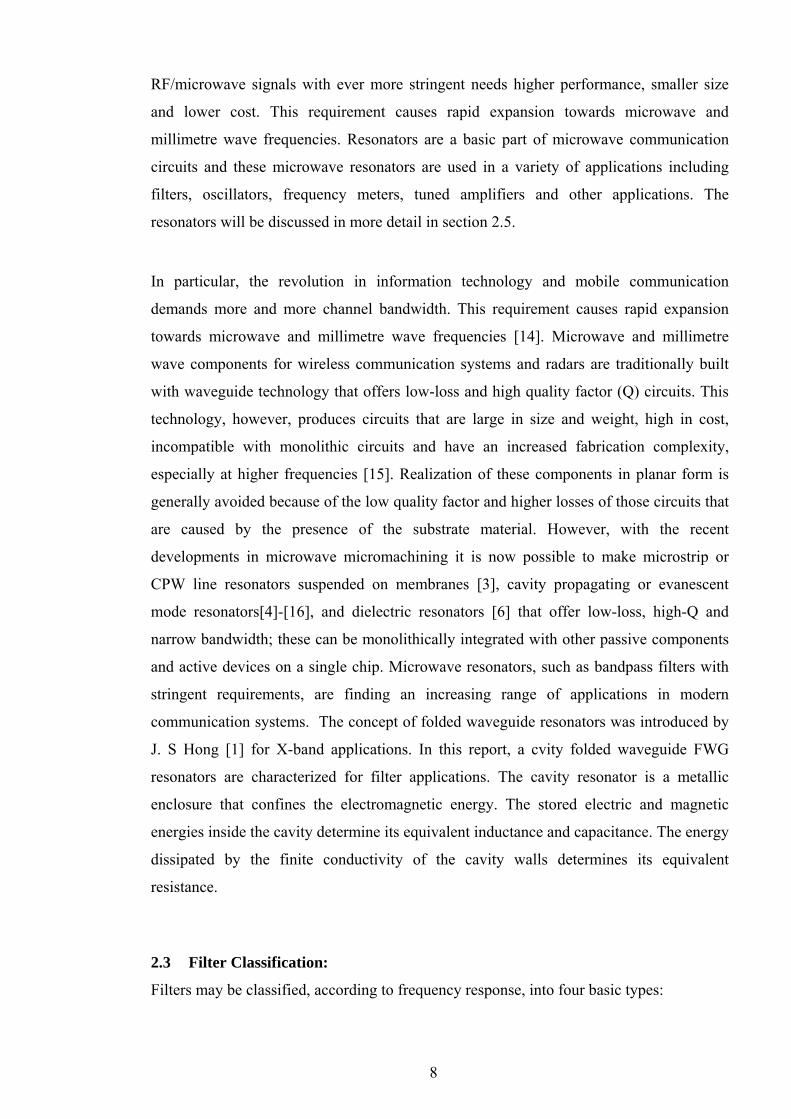


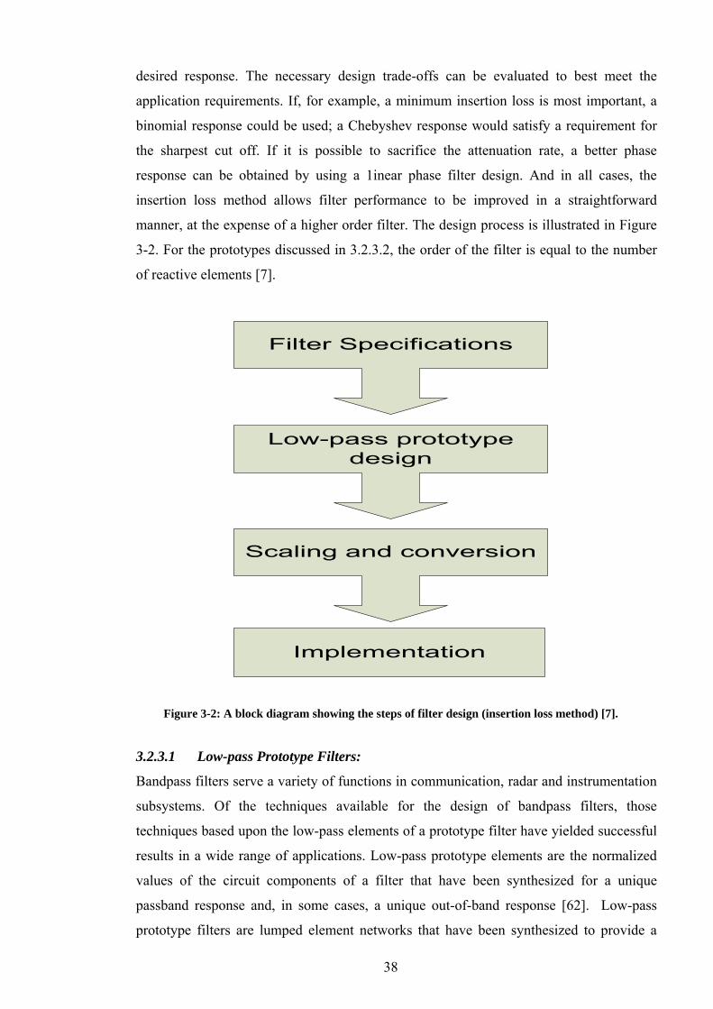


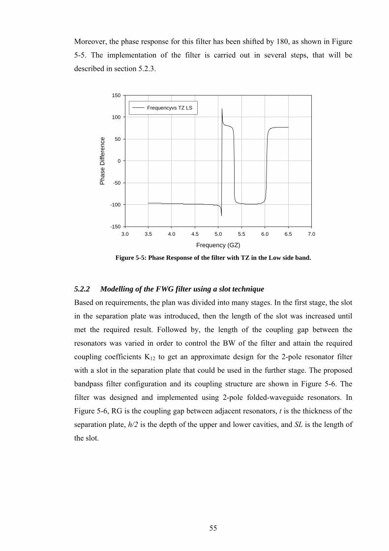


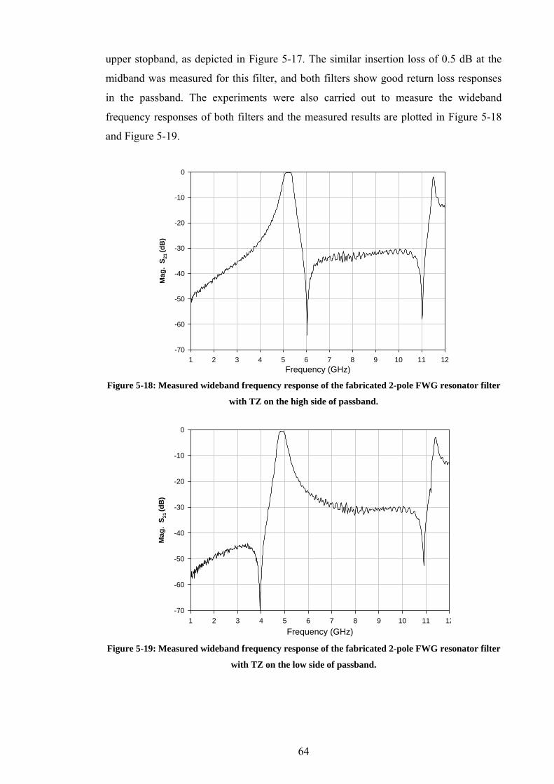


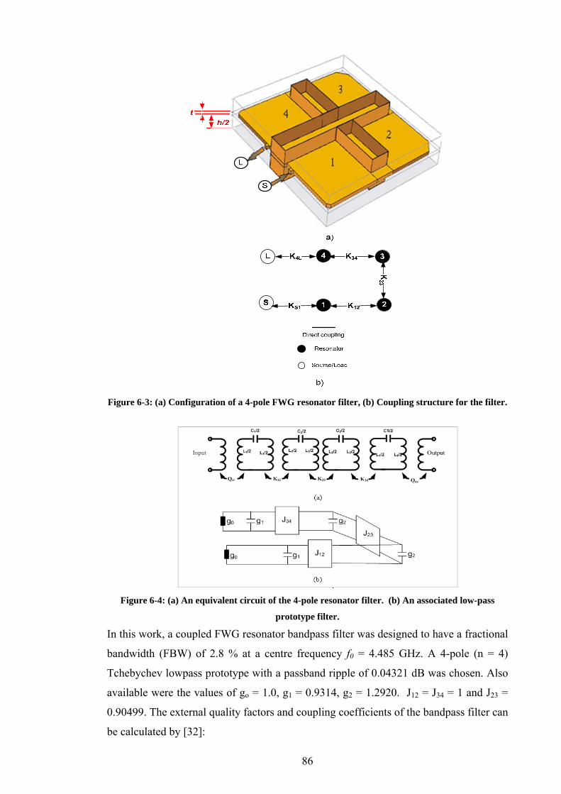


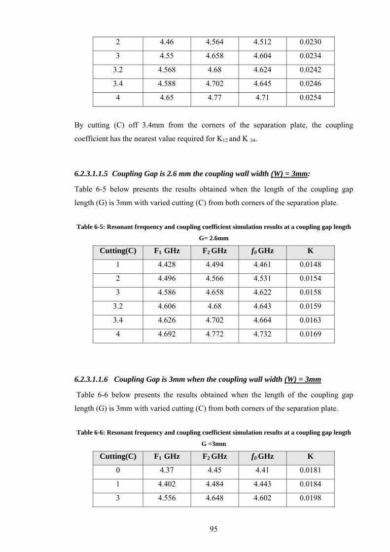


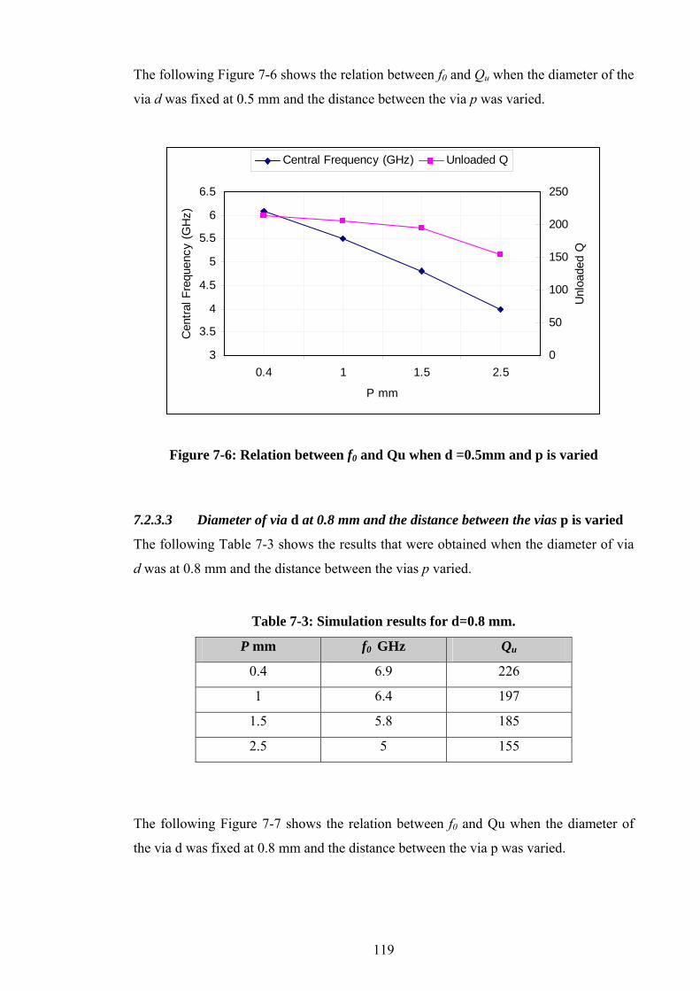


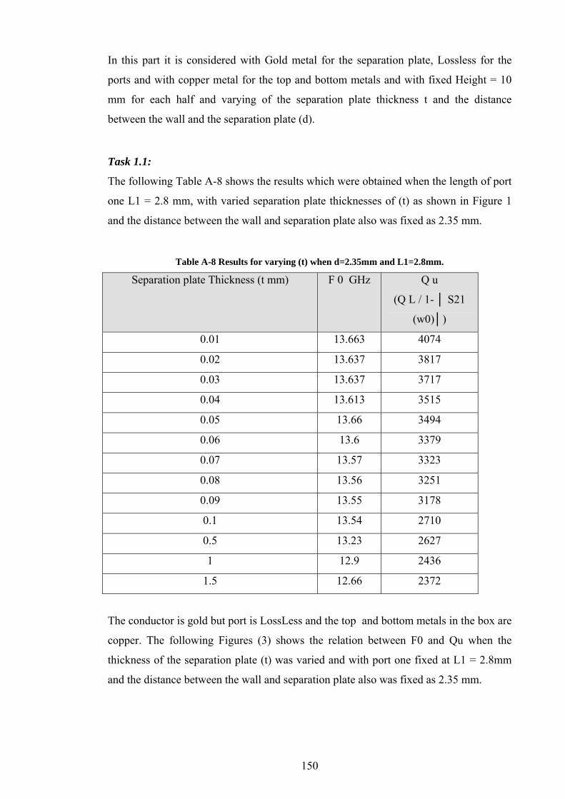


![Mid-infrared Vernier racetrack resonator tunable filter ... · Mid-infrared Vernier racetrack resonator tunable filter implemented on a germanium on SOI waveguide platform [Invited]](https://static.documents.pub/doc/80x56/5f4c8a2be860f8783803843f/mid-infrared-vernier-racetrack-resonator-tunable-filter-mid-infrared-vernier.jpg)


