30
Prof. Tai-Haur Kuo, EE, NCKU, 2000 Advanced Analog IC Design for Communications 2-1 Nyquist-Rate D/A Converts • Four main types – Decoder-based – Binary-weighted – Thermometer-code – Hybrid

Prof. Tai-Haur Kuo, EE, NCKU, 2000 Advanced Analog IC Design for Communications 2-1
Nyquist-Rate D/A Converts• Four main types
– Decoder-based– Binary-weighted– Thermometer-code– Hybrid

Prof. Tai-Haur Kuo, EE, NCKU, 2000 Advanced Analog IC Design for Communications 2-2
Decoder-Based DAC• Most straight forward approach
– create 2N reference signals and pass the appropriate signal to the output
• Three main types– Resistor string – Folded resistor-string– Multiple resistor-string
Prof. Tai-Haur Kuo, EE, NCKU, 2000 Advanced Analog IC Design for Communications 2-3
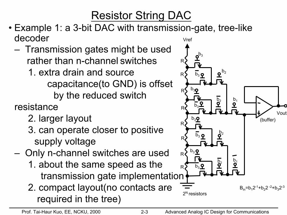
Resistor String DAC• Example 1: a 3-bit DAC with transmission-gate, tree-like
decoder
2N resistors
Vref
(buffer) Vout
R
R
R
R
R
R
R
R
b3
b3
b3
b3
b3
b3
b3
b3
b2
b2
b2
b2
b1
b1
Bin=b12-1+b22 -2+b32-3
– Transmission gates might be used rather than n-channel switches 1. extra drain and source
capacitance(to GND) is offset by the reduced switch
resistance2. larger layout3. can operate closer to positive
supply voltage – Only n-channel switches are used
1. about the same speed as the transmission gate implementation
2. compact layout(no contacts are required in the tree)
Prof. Tai-Haur Kuo, EE, NCKU, 2000 Advanced Analog IC Design for Communications 2-4
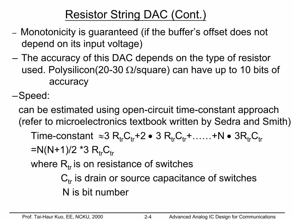
Resistor String DAC (Cont.)– Monotonicity is guaranteed (if the buffer’s offset does not
depend on its input voltage) – The accuracy of this DAC depends on the type of resistor
used. Polysilicon(20-30 Ω/square) can have up to 10 bits of accuracy
–Speed:can be estimated using open-circuit time-constant approach (refer to microelectronics textbook written by Sedra and Smith)
Time-constant ≈3 RtrCtr+2 • 3 RtrCtr+……+N • 3RtrCtr
=N(N+1)/2 *3 RtrCtr
where Rtr is on resistance of switches Ctr is drain or source capacitance of switches
N is bit number
Prof. Tai-Haur Kuo, EE, NCKU, 2000 Advanced Analog IC Design for Communications 2-5
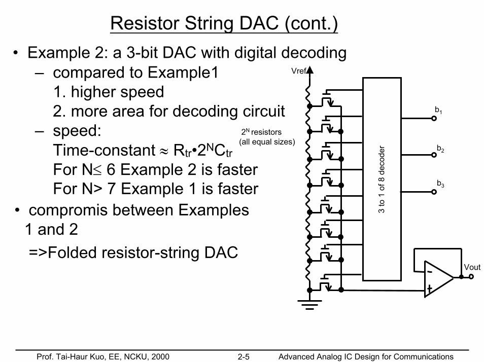
Resistor String DAC (cont.)
2N resistors (all equal sizes)
Vref
b1
b2
b3
Vout
3 to
1 o
f 8 d
ecod
er
– compared to Example1 1. higher speed 2. more area for decoding circuit
– speed:Time-constant ≈ Rtr•2NCtrFor N≤ 6 Example 2 is fasterFor N> 7 Example 1 is faster
• Example 2: a 3-bit DAC with digital decoding
• compromis between Examples 1 and 2=>Folded resistor-string DAC

Prof. Tai-Haur Kuo, EE, NCKU, 2000 Advanced Analog IC Design for Communications 2-6
Folded Resistor-String DAC
2 to
1 o
f 4 d
ecod
er
Vref
Bit lines
2N resistors (all equal sizes)
b2
Word linesequivalent
b1
2 to 1 of 4 decoder Output line
Vout
b3 b4
Prof. Tai-Haur Kuo, EE, NCKU, 2000 Advanced Analog IC Design for Communications 2-7
Folded Resistor-String DAC (Cont.)• Reduce the amount of digital decoding• Reduce large capacitive loading• Decoding is very similar to that for a digital memory• Example: 4 bit (=2 bit+2 bit) DAC Time constant ≈ Rtr (22 Ctr)+2 Rtr (22 Ctr)• other design examples
12 bit=6 bit+6 bit, or 4 bit+4 bit+4 bit, or…..10 bit=5 bit+5 bit, or 3 bit+3 bit+4 bit, or…...
etc.

Prof. Tai-Haur Kuo, EE, NCKU, 2000 Advanced Analog IC Design for Communications 2-8
Multiple Resistor-string DAC• 6-bit example• Requires only 2•2N/2resistors• Monotonic if OPAMPS have
matched, voltage-insensitive offset voltages.
• For high speed, OPAMPS must be fast.
For high resolution, OPAMPS must be low noise.
• The matching requirements of the second resistor string are not nearly as severe as those for the first string.
Vref Vout
2•2N/2
Resistors
(all equal sizes)
– The second resistor string is used to decode only lower-order bits

Prof. Tai-Haur Kuo, EE, NCKU, 2000 Advanced Analog IC Design for Communications 2-9
Signed Outputs• Negative output voltages are required. Two popular methods
1. The bottom of the resistor string can be connected to -Vref – requires a negative power supply– circuits are needed to realize a dual power supply– high cost if the negative supply is obtained off chip
2. Using SC inverting amplifier– realizes a signed output from a unipolar (positive) DAC
output– b1 high causes a negative output
2
1
b1
b1
b1
b1
Output line from DAC
2
1
1
2 Vout or -Vout

Prof. Tai-Haur Kuo, EE, NCKU, 2000 Advanced Analog IC Design for Communications 2-10
Binary-Weighted (or Binary-Scaled) Converters• An appropriate set of signals that are all related in a binary
fashion The binary array of signals might be voltages, charges, or
currents • Binary-weighted resistor DAC Reduced-resistance-ratio ladders R-2R-based DAC Charge-redistribution switched-capacitor DAC Current-mode DAC

Prof. Tai-Haur Kuo, EE, NCKU, 2000 Advanced Analog IC Design for Communications 2-11
Binary-Weighted Resistor DAC• 4-bit example
b1
2R
b2
4R
b3
8R
b4
16R
-Vref
RF
Vout
•• •• • •• • ••
• ••
•
•
• Does not require many resistors or switches
N2• Disadvantages
1. Resistor ratio and current ratio are on the order of .If N is large, this large current ratio requires that the switches also be scaled so that equal voltage drops appear across them.
2. monotonicity is not guaranteed3. prone to glitches
+++=
=
−−−−=
−−− 33
22
11
321
222 842bbbBwhere
BVRR
Rb
Rb
RbVRV
in
inrefF
refFout

Prof. Tai-Haur Kuo, EE, NCKU, 2000 Advanced Analog IC Design for Communications 2-12
• An additional 4R was added such that resistance seen to the right of the 3R equals R.
• One-fourth the resistance ratio compared to the binary-weighted case
• Current ratio has remained unchanged=>Switches must be scaled in size
• Repeating this procedure recursively, one can obtain an R-2R ladder
Reduced-Resistance-Ratio Ladders• Reduce the large resistor ratios in a binary-weighted array• Introduce a series resistor to scale signals in portions of the
array VA=-1/4 Vref
b1 b2 b3 b4
2R 4R 2R 4R
Vout
3R
R -Vref VA=1/4(-Vref)
4R
RF

Prof. Tai-Haur Kuo, EE, NCKU, 2000 Advanced Analog IC Design for Communications 2-13
R-2R-Based DAC• Smaller size and better accuracy than a binary-sized approach 1. small number of components 2. resistance ratio of only 2• 4-bit example
RV
I refr 2=
RF
b1 b2 b3 b4
2R 2R 2R 2R
Vout
R R R 2R
Ir Ir/2 Ir/4 Ir/8
Ir Ir/2 Ir/4 Ir/8
-Vref
∑ ∑= =
− ==N
i
N
iiiF
refiri
Foutb
RRVIbRV
1 11 2
)(2
• Current ratio is still large =>large ratio of switch sizes
Prof. Tai-Haur Kuo, EE, NCKU, 2000 Advanced Analog IC Design for Communications 2-14
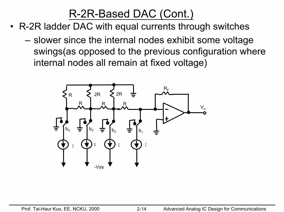
R-2R-Based DAC (Cont.)• R-2R ladder DAC with equal currents through switches
– slower since the internal nodes exhibit some voltage swings(as opposed to the previous configuration where internal nodes all remain at fixed voltage)
Vo
2R 2R R
R R R
RF
-Vss
I I I I
b1 b2 b3 b4

Prof. Tai-Haur Kuo, EE, NCKU, 2000 Advanced Analog IC Design for Communications 2-15
Charge-Redistribution Switched-Capacitor DAC• Insensitive to OPAMP input-offset voltage, 1/f noise, and finite
amplifier gain• An additional sign bit can be realized by interchanging the
clock phases(shown in parentheses)
b1 b4
Vout
Vref
8C
b2 b3
4C C 2C
16C
C2
)Φ(Φ 21
)Φ(Φ 12
a2Φ
a1Φ
1Φ
2Φ

Prof. Tai-Haur Kuo, EE, NCKU, 2000 Advanced Analog IC Design for Communications 2-16
Current-Mode DAC• High-speed • Switch current to output or to ground The output current is converted to a voltage through RF
• The upper portion of current source always remains at ground potential.
RF
-5V
I/2 I/4 I/8
b4 b3 b2 b1
I
Vout

Prof. Tai-Haur Kuo, EE, NCKU, 2000 Advanced Analog IC Design for Communications 2-17
Glitches• A major limitation during high-speed operation• Mainly the result of different delays occuring when switching
different signals • Example: 01111……1--->1000 ……0 1. I1represents the MSB current, and I2 represents the sum of
(N-1) LSB currents. 2. The MSB current turns off slightly early, causing a glitch of
zero current
I1+I2
I1
I2
t
t
t
RF
I2 I1
Vout
Prof. Tai-Haur Kuo, EE, NCKU, 2000 Advanced Analog IC Design for Communications 2-18
Glitches (Cont.)• Glitch disturbance can be reduced by 1. limiting the bandwidth (placing a capacitor across RF ) This method slows down the circuit. 2. using a sample and hold on the output signal. 3. modifying some or all of the digital word from a binary
code to a thermometer code.(3. is the most popular method.)

Prof. Tai-Haur Kuo, EE, NCKU, 2000 Advanced Analog IC Design for Communications 2-19
Thermometer-Code DACs• Digitally recode the input to a thermometer-code equivalent
• Advantages over its binary-weighted counterpart 1. low DNL errors 2. guaranteed monotonicity 3. reduced glitching noise• Does not increase the size of the analog circuitry compared
to a binary-weighted approach
Thermometer-code representations for 3-bit binary values
Binary Thermometer Code
Decimal b1 b2 b3 d1 d2 d3 d4 d5 d6 d7
0 1 2 3 4 5 6 7
0 0 0 0 0 1 0 1 0 0 1 1 1 0 0 1 0 1 1 1 0 1 1 1
0 0 0 0 0 0 0 0 0 0 0 0 0 1 0 0 0 0 0 1 1 0 0 0 0 1 1 1 0 0 0 1 1 1 1 0 0 1 1 1 1 1 0 1 1 1 1 1 1 1 1 1 1 1 1 1
Prof. Tai-Haur Kuo, EE, NCKU, 2000 Advanced Analog IC Design for Communications 2-20
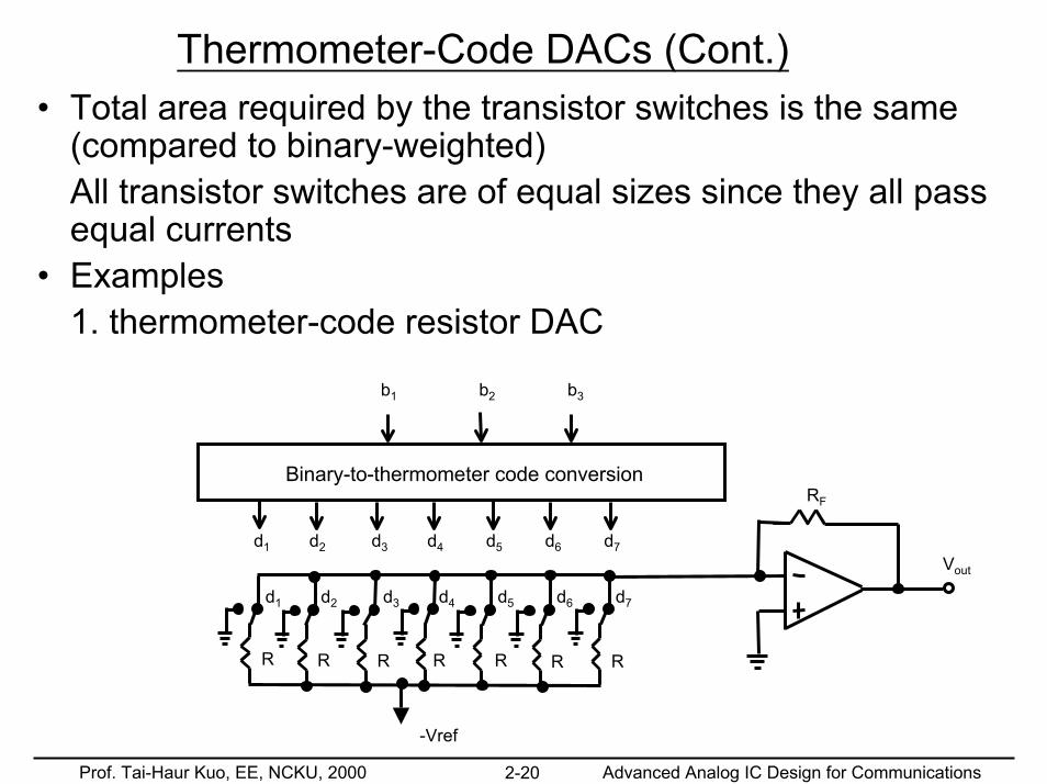
Thermometer-Code DACs (Cont.)• Total area required by the transistor switches is the same
(compared to binary-weighted) All transistor switches are of equal sizes since they all pass
equal currents• Examples 1. thermometer-code resistor DAC
Binary-to-thermometer code conversion
b1 b2 b3
d1 d2 d3 d4 d5 d6 d7
R
RF
Vout
-Vref
R R R R R R
d1 d2 d3 d4 d5 d6 d7

Prof. Tai-Haur Kuo, EE, NCKU, 2000 Advanced Analog IC Design for Communications 2-21
Thermometer-Code DACs (Cont.)2. thermalmeter-code charge-redistribution DAC
CN2
refV1φ
2φ
2φ
outV
2C
1φ
2φ
Top capacitors are connected to ground
Bottom capacitors are connect to Vref
1φC
C
C
C
C

Prof. Tai-Haur Kuo, EE, NCKU, 2000 Advanced Analog IC Design for Communications 2-22
Thermometer-Code Current-Mode DAC• Row and column decoders• Inherent monotonicity• Good DNL errors
INL errors depend on the placement of the current sources• In high-speed applications
1. The output current feeds directly into an off-chip 50 or75 resistor, rather than an output OPAMP.
Ω
Ω2. Cascode current sources are
used to reduce current-sourcevariation due to voltage changesin
outVoutV
All current sources are of equal values.

Prof. Tai-Haur Kuo, EE, NCKU, 2000 Advanced Analog IC Design for Communications 2-23
Thermometer-Code Current-Mode DAC (Cont.)
4Q
3Q
2Q1Qid
id
outV
I-Src array
Column decoder
Row
dec
oder
Bias voltages

Prof. Tai-Haur Kuo, EE, NCKU, 2000 Advanced Analog IC Design for Communications 2-24
Thermometer-Code Current-Mode DAC (Cont.)• Precisely timed edges are needed
1. If both and are low simultaneously, the drain of is pulled low and the circuit takes longer time to respond.
2. If both and are high simultaneously, is shortedto ground.
• To avoid the use of the two logic levels, the gate ofshould be connected to a dc bias voltage
id id
idid
3Q
2Q
outV
Prof. Tai-Haur Kuo, EE, NCKU, 2000 Advanced Analog IC Design for Communications 2-25
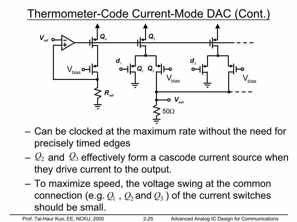
Thermometer-Code Current-Mode DAC (Cont.)
– Can be clocked at the maximum rate without the need for precisely timed edges
– and effectively form a cascode current source when they drive current to the output.
– To maximize speed, the voltage swing at the common connection (e.g. , and ) of the current switches should be small.
2Q 3Q
1Q 2Q 3Q
refV
1Q 2Q
3Q4Q
1d 2d
outV
Ω50
refR
biasVbiasVbiasV
Prof. Tai-Haur Kuo, EE, NCKU, 2000 Advanced Analog IC Design for Communications 2-26
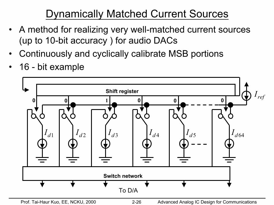
Dynamically Matched Current Sources• A method for realizing very well-matched current sources
(up to 10-bit accuracy ) for audio DACs• Continuously and cyclically calibrate MSB portions• 16 - bit example
1dI 2dI 3dI 4dI 5dI 64dI
Switch network
Shift registerrefI0 0 010 0
To D/A
Prof. Tai-Haur Kuo, EE, NCKU, 2000 Advanced Analog IC Design for Communications 2-27
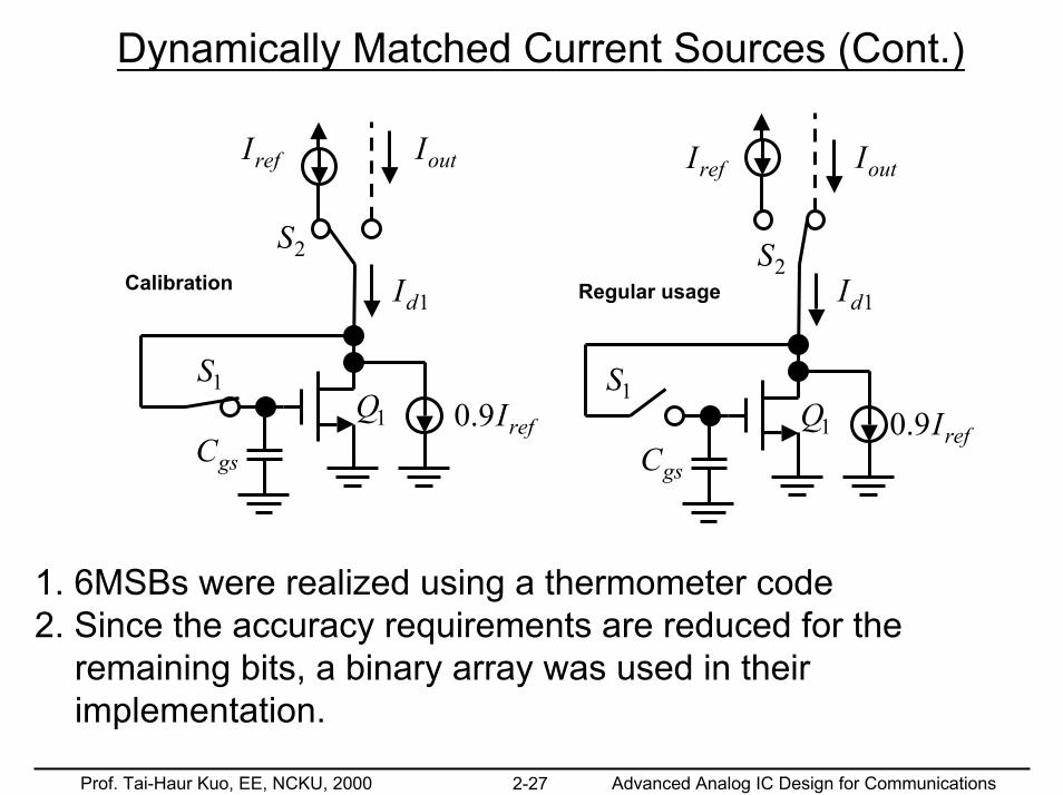
Dynamically Matched Current Sources (Cont.)
1S
refI outI
2S
refI outI
1dI 1dI
refI9.0refI9.0
1S
2S
gsC gsC1Q1Q
Calibration Regular usage
1. 6MSBs were realized using a thermometer code2. Since the accuracy requirements are reduced for the
remaining bits, a binary array was used in their implementation.

Prof. Tai-Haur Kuo, EE, NCKU, 2000 Advanced Analog IC Design for Communications 2-28
Dynamically Matched Current Sources (Cont.)3. 64 accurately matched current sources for the 6 MSBs
– current sources are calibrated– dynamically setting current sources– even though only 63 are required, the extra one is needed
so that DAC can continuously operate when one of them is being calibrated
4. major limitation in matching 64 current sources is due tothe differences in clock feedthrough and charge injectionswitches – the best way is to minimize them
large and large of only source a small current
can be used for
iS
gsC gsV1Q
1Q
large
smallL
W1Q

Prof. Tai-Haur Kuo, EE, NCKU, 2000 Advanced Analog IC Design for Communications 2-29
Dynamically Matched Current Sources (Cont.)
– dummy transistor can be added to – other methods to minimize these errors are referred to
switched-current (SI) papers
iS
– large to minimize leakage current effect before current sources are recalibrated
gsC

Prof. Tai-Haur Kuo, EE, NCKU, 2000 Advanced Analog IC Design for Communications 2-30
Hybrid Converters• Combine the advantages of different approaches • It’s quite common to use a thermometer-code approach for
the top few MSBs while using a binary-scaled technique for the lower LSBs– glitching is significantly reduced and accuracy is high– circuit area is saved with a binary-scaled approach for
LSBs • Examples
1. Resistor-capacitor hybrid DAC2. Segmented DAC


![Assignment Problems with Weighted and Nonweighted …jfrabajante.weebly.com/.../11551779/assignment_problems.pdf · 2018. 9. 7. · particular, binary integer programming [7, 6].](https://static.documents.pub/doc/80x56/60145d3d09c5b1525574972b/assignment-problems-with-weighted-and-nonweighted-2018-9-7-particular-binary.jpg)


