Coverage of Week 2 (CSCE 613)Coverage of Week 2 (CSCE 613)Rabaey et al., Chapter 2: § 2.1, 2.2, pp. 36-46.
Slides 2- 14
Rabaey et al., Chapter 3: § 3.3 (3.3.1, 3.3.2), pp. 74-80, 87-90.Slides 3-7, 9, 10 (diodes)Slides 14-22 (MOS transistors)
Note for coverage of course materialAs this is CSCE course (and not an EE course), we’ll focus more on aspects of device structure, function and behavior that allow us to develop computational models using the constructs at the switch-level of VLSI system abstraction.
The EE courses focus more on device characteristics and the circuits aspects of the technology.
We may not be covering the Spice-related aspects of modeling devices in this course. We’ll focus more on circuit layout and use of design rules.
3
Topics of Week 2 (from Topics of Week 2 (from RabaeyRabaey))
Discuss the MOS transistor – behavior, function and structure (materials from Chapters 2 & 3 of Rabaey et al.)
Discussion of fabrication process (introduction), so we can have some image of the device structure, in situ, along with the device behavior.
P-MOS and N-MOS transistors -> switching characteristics.Introduction of basic device equationsIntroduction of models for manual analysis
EE141
2
4
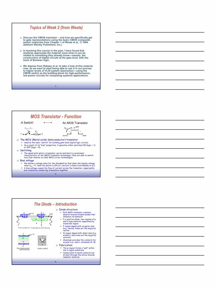
Topics of Week 2 (from Topics of Week 2 (from WesteWeste))
In teaching this course in the past, I have found that students appreciate the material more when it can be related to something they already know—namely, the construction of digital circuits at the gate level, with the tools of Boolean logic.
We digress from Rabaey et al. to take a look at this material now, as we want to start being able to use it in our journey to higher levels of VLSI system abstraction—using the CMOS switch as the building block for high-performance, low-power circuits for computing systems applications.
5
MOS Transistor MOS Transistor -- FunctionFunction
VGS ≥ VTRon
S D
A Switch! An MOS Transistor
The MOS (Metal-oxide Semiconductor) transistorUsed as the basic “switch” for building gate-level digital logic circuits.As a result of its “bias” properties, it operates either switched ON (logic = 1) or OFF (logic = 0).
SwitchingThe speed with which a transistor can be switched is a prominentcharacteristic of the CMOS transistor technology—they are able to switch very fast relative to other MOS circuit technologies.
Bias voltageWe define a voltage value for the threshold so that when the biasing voltage value VGS > VT then the switch is ON (cf. Lecture 3 slides from Rabaey et al.)A bias voltage causes the flow of current across the transistor; signal paths are created by connecting transistors together.
|VGS|gate
source drain
6
The Diode The Diode –– IntroductionIntroduction
p
n
B A SiO2Al
Cross-section of pn-junction in an IC process
n
p
A
B
Al
One-dimensionalrepresentation
A
B
diode symbol
Diode structureEach MOS transistor contains several reverse-biased diodes that influence its behavior. P-n junction diode: two regions of p-and n-type material, separated by transition region.P-region doped with acceptor ions (e.g., boron); holes are the majority carrier.N-region doped with donor ions (e.g., arsenic); electrons are the majority carriers.Aluminum provides the contacts for access to p- and n- terminals (A, B).
FabricationThe p-region forms a “well” within the n-region substrate.Connections to metal contacts are etched through the silicon dioxide insulator material.
EE141
3
7
The Diode The Diode -- Depletion RegionDepletion Region
hole diffusionelectron diffusion
p n
hole driftelectron drift
ChargeDensity
Distancex+
-
ElectricalxField
x
PotentialV
ξ
ρ
W2-W1
ψ0
(a) Current flow.
(b) Charge density.
(c) Electric field.
(d) Electrostaticpotential.
Diode functionBringing p- and n- materials together causes large concentration gradient at region boundary. Gradient causes electrons to diffuse n->p; holes diffuse p->n.
Considering behavior under condition of “zero bias”:
Depletion region: at the junctionMobile carriers removedFixed acceptor, donor ions remainCharges create electric field across boundary (n->p)Field counteracts diffusionof holes, electrons via drift.
Depletion charge sets up electric field, so that driftcurrent = diffusion current (opposite direction).No net current flow when zero bias voltage.
Forward bias (diffusion) current (p->n)
Reverse bias (drift) current (n->p)
P-type material more heavily dopedthan n-type.
Charge concentration in Depletion region ishigher on p-side of the junction.
Built-in potential, Φ0, exists under zero bias.
8
The Diode The Diode –– Forward Bias CurrentForward Bias CurrentApplying a bias voltage, VD:
Potential of p-region raised relative to the n-region.Flow of mobile carriers across p-n junction increases as diffusioncurrent dominates drift current.Carriers traverse Depletion region, injected into neutral n- and p-regions.Minority carriers diffuse neutral regions (concentration gradient) and get recombined w/ majority carriers.Net result is current flow p->n.
PlotsDiode current has exponential dependency on bias voltage.Current ID increases 10x for every 60mV of VD bias.At small VD bias, recombination of holes and electrons in Depletion region.
Ideal diode equation:Relates diode current to diode bias voltage.Is – saturation current (technology constant).ΦT – thermal voltage.
9
The Diode The Diode -- Device BiasDevice Bias
x
pn0
np0
-W1 W20
p n(W
2)
n-regionp-region
Lp
diffusion
Forward bias - typically avoided in digital ICs.
x
pn0
np0
-W1 W20n-regionp-region
diffusion
Reverse bias - the dominant operation mode.
Forward bias:Potential of p-region raised with respect to n-region.Minority carriers injected across Depletion region into neutral region, combine with majority carriers, resulting in current flow (diffusion).
Reverse bias:Potential of p-region is lowered with respect to n-region.Reduction in diffusion current, so that drift current becomes dominant.Number of minority carriers in neutral regions is small. Drift current is ignored.
Minority carrier concentration inneutral regions near pn-junction.
EE141
4
10
The MOS Transistor The MOS Transistor -- StructureStructure
Polysilicon Aluminum
4-terminal deviceVoltage applied to the gate terminal determines if and how much current flows between source and drain ports.The body is the 4th terminal, serving to modulate device properties.When Vgs > VT, then a conducting channel is formed between drain and source.The larger the Vgs, the smaller the resistance of conducting channel, the larger the current.
CMOS device configurationP-type transistor: n-type substrate separating 2 “well” areas of p-type material.N-type transistor: p-type substrate separating 2 “well” areas of n-type material.Current flow for pMOS vs nMOS is under opposite bias conditions.
CMOS device structureLayers (1) diffusion (doped silicon), (2) polysilicon (used for interconnect), (3) aluminum, separated by insulating layers.N-channel (nMOS) vs p-channel (pMOS) devices are reversed in configuration
Diffusion
11
MOS Transistor MOS Transistor -- StructureStructure
tox
n+ n+
Cross section
L
Gate oxide
xd xd
Ld
Polysilicon gate
Top view
Gate-bulkoverlap
Source
n+
Drain
n+W
Top viewThe polysilicon region rides on top of the diffusion regions, with some overhang.The “poly” doesn’t sit directly on the diffusion, but is separated by an insulation layer of SiO2.The length and widths of the regions plays a role in transistor performance.
Cross section viewThe n+ drain and source regions embedded in p-type substrate (nMOS).Electron current flows from source to drain through the n-type channel underneath the gate, in the presence of bias voltage (nMOS device as shown).Hole current flows from drain to source through the p-type channel for pMOS device.
P-doped substrate underneath foran n-channel transistor.
nMOS device
12
CMOS ProcessCMOS Process
p-well n-well
p+
p-epi
SiO2
AlCu
poly
n+
SiO2
p+
gate-oxide
Tungsten
TiSi2
DualDual--Well TrenchWell Trench--Isolated Isolated CMOS ProcessCMOS Process
(side view)(side view)
CMOS devicesUse both nMOS and pMOS transistors together to form gate structures.Place an n-channel (nMOS) device next to p-channel (pMOS) device, separated by insulator layer to separate the devices.Unprogrammed, these devices reside in a “sea of gates” structure, where thousands of devices of each type are arrayed, separated by channels
Process exampleDiffusion layer – uses a p-doped material as a substrate, with epitaxial layer on top of it. Finally, n- and p-doped regions form the substrate regions for individual transistors. The alternately doped p+ and n+ regions form the “well” regions for individual transistors.Poly layer – uses a polysilicon created by taking SiO2 and doping it with more Si to make it conducting rather than insulating.Metal layers – multiple layers for different conducting and signal routing paths, used to create elaborate circuit topologies on top of the substrate.
EE141
5
13
CMOS Process at a Glance (CMOS Process at a Glance (Rabaey Rabaey –– Ch 2)Ch 2)Define active areasEtch and fill trenches
Implant well regions
Deposit and patternpolysilicon layer
Implant source and drainregions and substrate contacts
Create contact and via windowsDeposit and pattern metal layers
14
MOS Fabrication MOS Fabrication -- Patterning of SiOPatterning of SiO22
Si-substrate
Si-substrate
(a) Silicon base material
(b) After oxidation and depositionof negative photoresist
(c) Stepper exposure
PhotoresistSiO2
UV-lightPatternedoptical mask
Exposed resist
Si-substrate
Si-substrate
SiO2Si-substrate
Si-substrate
SiO2
SiO2
(d) After development and etching of resist,chemical or plasma etch of SiO2
(e) After etching
(f) Final result after removal of resist
Hardened resist
Hardened resist
Chemical or plasmaetch
15
CMOS Process WalkCMOS Process Walk--ThroughThrough
p+
p-epi
(a) Base material: p+ substrate with p-epi layer
p+
(c) After plasma etch of insulatingtrenches using the inverse of the active area mask
(b) After deposition of gate-oxide andsacrificial nitride (acts as abuffer layer)
p+
p-epi SiO2
3Si N4
SiO2
(d) After trench filling, CMPplanarization, and removal of sacrificial nitride
(e) After n-well and VTp adjust implants
n
(f) After p-well and VTn adjust implants
p
EE141
6
16
CMOS Process WalkCMOS Process Walk--ThroughThrough
(g) After polysilicon depositionand etch
poly(silicon)
(h) After n+ source/drain andp+ source/drain implants. These
p+n+
steps also dope the polysilicon.
(i) After deposition of SiO2insulator and contact hole etch.
SiO2
(j) After deposition and patterning of first Al layer.
Al
(k) After deposition of SiO2insulator, etching of via’s,deposition and patterning ofsecond layer of Al.
AlSiO2
17
Advanced MetallizationAdvanced MetallizationHigh-density ICs require many layers of metal to form the interconnect of the circuit.
Power VDDGround VSSLong lines connecting device outputs to next stage inputs.
As we will see, all of this metal (Aluminum) creates circuit effects that affect load and circuit delay.
ResistanceCapacitanceInductance
We can use mathematical analysis to estimate effects.We place & route circuits according to design rules.
18
MOS Circuit MOS Circuit -- Design & LayoutDesign & LayoutVDD VDD
Vin Vout
M1
M2
M3
M4
Vout2
What is the function of this circuit?This is a signal buffer, created by tying the output of one inverter to the input of another.The inverter is created by tying the source terminals of the p-channel and n-channel transistors together.The gates of both transistors get the bias voltage, but the p- and n- devices are biased opposite of each other.
Schematic viewThis shows how the transistors are connected to form the inverter and the buffer driver, placed in the signal path to refresh a signal to its required driving level.Threshold voltage has positive value for nMOS device, negative value for pMOS.
Layout viewThis shows the top-level layout of the Buffer driver circuit.The green is the diffusion layers, the red is the poly layer, and the black squares show the contacts for the metal layers.
n-channel transistor
p-channel transistor
source
source
drain
drain
EE141
7
19
The CMOS Switch The CMOS Switch –– Structural ViewStructural ViewMOS structure
MOS structure is created by superimposing several layers of conducting, insulating, and transistor-forming materials to create “sandwich” structure.Steps include (1) oxidation of silicon, (2) diffusion of impurities into silicon, giving it certain conduction properties (creating “diffusion” and “poly” layers), (3) deposition & etching of metal (e.g., aluminum) for interconnect between transistor elements.N-switch: p-type substrate separating 2 areas of n-type (negative areas rich in electrons). Area separating n-type areas is capped with SiO2 (insulator) and conducting electrode (polysilicon) “gate”.P-switch: the n-type substrate has 2 p-type regions (“wells”)The gate is the control input, affecting flow of current between source and drain.
20
The CMOS Composite Switch The CMOS Composite Switch –– Symbolic ViewSymbolic ViewpMOS and nMOS switching
We start with the nMOS transistor (n-switch) and pMOS transistor (p-switch).The MOS gate controls the passage of current between the source and drain terminals, and we view this action as “switching”, limited by the slew rate of the transistor (i.e., how fast it can change values from logic ‘1’ to ‘0’ and vice versa).N-switch is “on” when drain & source are connected (i.e, bias voltage produces current across the channel). N-switch is a “perfect” switch when ‘0’ is to be passed from an output to an input, but is a poor switch when ‘1’ is propagated.P-switch is closed, “on”, when a ‘0’ is at the gate, and open, “off”, when a ‘1’ is present. It is “perfect” when passing ‘1’ signal but not when passing ‘0’ signal.The pMOS and nMOS switches are “on” and “off” for complementary values of the gate signal. The p-switch uses “inversion” bubble.
21
The CMOS Composite Switch (The CMOS Composite Switch (WesteWeste))Creating CMOS switches
By combining an n-switch and p-switch together in parallel, we get one that passes ‘0’ and ‘1’ in acceptable strengths.If we only need to pass one or the other input to output, we can use a switch with one or the other pMOS/nMOS switch.The combined switch is called a c-switch, complementary switch, the “C” in CMOS.The control input is routed to to all switches; applied to n-switch and complement is applied to p-switch.Also referred to as “pass” gate or “transmission” gate.
Different symbology sometimes seenin circuit diagrams.
EE141
8
22
The CMOS Inverter Switch (The CMOS Inverter Switch (WesteWeste))Function
The inverter takes the input and logically inverts the input to produce an output (the logical “not” function).The n-switch only has to pass a ‘0’, where the VSS source of ‘0’ is stronger than the inverter’s output signal.The p-switch only has to pass a ‘1’, where the VDD source is stronger than the ‘0’ in the input.A fully complementary CMOS gate always has both n- and p-switches.The n-switch serves as “pulldown” to connect the output to ‘0’ (VSS or Ground).The p-switch serves as “pullup” to connect the output to ‘1’ (VDD).When both switch types are used, both try to exert a logic level at the output
23
Combinational Logic in CMOS (Combinational Logic in CMOS (WesteWeste))Logic functions
AND: 2 n-switches placed in series, where composite switch is closed, “on”, when both switches are closed (“on”).NORNOR: 2 p-switches in parallel, where if either input is ‘0’ (open), then the output is ‘1’ (closed).OR: 2 n-switches placed in parallel, where composite switch is “on” if either of the input switches is closed “on”.NAND: 2 p-switches placed in series, where if both inputs are ‘0’, the output is ‘1’ (closed).
24
CMOS Building Blocks CMOS Building Blocks –– NAND GateNAND GatePurpose
We need a reliable means to construct a unit block that can be used to build larger structures.2-input NAND serves this purpose!
FunctionWe combine the AND and NOR structures together to form 2-input NAND.Pulldown is a pair of n-switch transistors in series, one end connected to ground (VSS, or reference voltage), the other end connected to the output.Pullup structure is pair of p-switches, one end connected to VDD (supply voltage), other end connected to the output.The NAND inputs, A and B, are connected to the gates, one each, of the series n-switch and the parallel p-switch.
EE141
9
25
CMOS Building Blocks CMOS Building Blocks –– NOR GateNOR GatePurpose
We use the NOR gate in conjunction with the NAND, to derive all other Boolean logic gates (this can be verified form axioms of Boolean algebra).We want gate switch solutions that provide fully restored logic values to the output by passing either supply or ground directly to the output, depending on inputs supplied to n- and p-switch transistor gates.
FunctionThis structure has 2 p-switches in series, connected to VDD, joined at the output by the 2 n-switches in parallel connected to ‘0’ (ground).Pulldown dominates the functioning of series n-switches (see previous slide #7 for AND case).Pullup pair in parallel provides the complemented signals (see slide #7 for NOR case).For all input combinations, there is always a path from ‘1’ or ‘0’ inputs (VDD or VSS ground) to the output, and the full supply voltages appear at the output.
26
Building MultiBuilding Multi--input CMOS Logic Gatesinput CMOS Logic GatesPurpose
We can realize Boolean function of any number of input variables by using NAND and NOR structures of these inputs.
FunctionN-input NAND gate: is constructed by placing n-switch in series, to ground, and one p-switch in parallel, to output, for each Boolean variable required.N-input NOR gate: is constructed by placing n-switch in parallel, to output, and one p-switch in series, to supply voltage VDD, for each input variable.
NAND/NOR outputs areconnected here!
27
CMOS Compound Gate CMOS Compound Gate –– Example 1Example 1Purpose
To create gate structures for arbitrary logic functions, we need a method of constructing compound gate arrays using the CMOS switches.
FunctionA compound gate is formed by using a combination of series- and parallel-switch structures.We decompose the Boolean expression into n- and p-side components, and assemble a comound structure from the basic patterns we have discussed.For n-side, we take the expression and assemble that part of the composite.For p-side, we invert the expression, and assemble that part of it.We connect one end of p-structure to ‘1’ (VDD) and other to the output.We connect one side of the n-structure to ‘0’ (Vss ground) and the other to output in common with the p-structure.
(A*B) (C*D)See AND patternon slide #23. (A*B) + (C*D)
See OR patternon slide #23.
(A+B) * (C+D)
See OR, AND patterns on slide #7, where we have OR pattern connecting p-switches in parallel, followed by AND pattern connecting the ORed structures in series.
Finally, combining the two structures together yields the resultant CMOS circuit for the logic expression above.
EE141
10
28
The CMOS Switch The CMOS Switch –– BenefitsBenefitsCMOS Benefits
The use of p-switches and n-switch combinations are “duals” of each other, i.e., the patterns are easily discernable one from another.For all inputs, there is always a path from ‘1’ or ‘0’ (VDD or VSS supplies) to the output and that the full supply voltages appear at the output (known as fully restored logic).In other logic families, the sizes of pullup and pulldown transistors must be ratioedfor the gate to function correctly. This is not the case with CMOS—a benefit for scaling of CMOS and for fabrication. There is never a path from the ‘1’ to the ‘0’ supplies for any combination of inputs (in contrast to other types of logic gates)—and is the basis for the low static power dissipation in CMOS.
a
b
s
29
CMOS Gate Design CMOS Gate Design –– Example 2Example 2F=((A + B + C) * D)
Analyze by identifying the sub-functions and mapping these to combinations of serial or parallel switches.The n-function (A+B+C) is implemented as 3 parallel n-switches, which is placed in series with an n-switch for D on the input.Complementing, we get the p-function (D+ A*B*C), that requires 3 p-switches in series connected, in turn, with a p-switch with D on its input.K-maps can be used to analyze both n- and p-logic structures.
Sometimes the inputs or outputsrequire inversion in order to bemapped using the underlyingavailable gates (E.g., NAND andNOR gates).
Such gate descriptions may beoptimized for speed or densityas part of logic synthesis.
30
Constructing the CMOS MultiplexerConstructing the CMOS MultiplexerStructure
Complementary switches (c-switch) can be used to select among a number of inputs, forming the MUX function.The switches must pass ‘1’ and ‘0’ equally well, so the c-switch is used.MUXes are used in building CMOS memory elements and in data manipulation structures.
EE141
11
31
Constructing a CMOS DConstructing a CMOS D--LatchLatchStructure
We can build a “level-triggered” D-latch using a 2-input MUX (built of c-switches) and also using 2 inverters.D is data input, CLK is clock input, and outputs are Q and –Q.Note that CLK serves as the “S” input to the gates of the p- and n-switch transistors comprising the c-switch.
BehaviorWhen CLK =1, Q is set to D, and –Q is set to –D (logical NOT).When CLK switches to ‘0’, feedback path around inverter pair is set up, causing current state of Q to be stored.The D input is ignored while CLK = 0.Level-sensitive: state of output dependent on level of CLK.
32
Constructing a CMOS DConstructing a CMOS D--Flip FlopFlip FlopStructure (pos edge D-FF)
We construct an edge-triggered register by combining two level-sensitive latches in series.The first stage (“master”) D-latch is positive sensitive, and the second (“slave”) is negative sensitive.
BehaviorWhile CLK = 0, the master D-latch output, -QM, follows the D input, while slave D-latch holds its previous value.When CLK transitions 0 -> 1, master D-latch ceases to sample D input, stores D value at time of transition. The slave latch opens, passing stored value -QM to output QS.While CLK =1, D in put is prevents from affecting the output, since master is disconnected from D input.When CLK goes 1 -> 0, the slave latch locks in the master latch output, while master starts sampling D input again.
33
Week 2 SummaryWeek 2 SummaryWe have looked at the basic MOS device from different points of view:
Structural: how it is constructed (via fabrication) and what it’s structure is composed of.Functional: how the CMOS devices carry out their switching function, and how we build familiar digital logic functions from combinations of CMOS gates.Behavioral: how the CMOS switch is really a 4-terminal device, where there’s a reverse bias diode embedded in it that governs its charge carrying behavior.
Next week: we elaborate the detailed behavior of the MOS gates, and develop appropriate models for analysis, estimation and prediction.