Page 1
Use of FTDI devices in life support and/or safety applications is entirely at the user’s risk, and the user agrees to defend, indemnify and hold harmless FTDI from any and all damages, claims, suits or
expense resulting from such use.
Future Technology Devices International Limited (FTDI) Unit 1, 2 Seaward Place, Glasgow G41 1HH, United Kingdom Tel.: +44 (0) 141 429 2777 Fax: + 44 (0) 141 429 2758
Web Site: http://ftdichip.com Copyright © Future Technology Devices International Limited
Application Note
AN_184
FTDI Device Input Output Pin States
Version 3.1
Issue Date: 2018-04-19
This application note describes the reset, suspend and active states of the input / output pins of the following devices: FT232R, FT245R, FT232H, FT2232H, FT4232H, FT2232D, FT200XD, FT201X, FT220X, FT221X, FT230X, FT234XD, FT231X, FT240X, FT120, FT121, FT122, FT313H & FT4222H
Page 2
Application Note
AN_184 FTDI Device Input Output Pin States Version 3.1
Document Reference No.: FT_000507 Clearance No.: FTDI#237
1 Product Page Document Feedback Copyright © Future Technology Devices International Limited
Table of Contents
1 Introduction ................................................................... 3
1.1 Applicable Documents .............................................................. 3
2 FT232R – I/O Pins .......................................................... 4
2.1 FT232R - CBUS Selected Function ............................................. 5
3 FT245R - I/O Pins .......................................................... 6
4 FT232H– I/O Pins ........................................................... 7
4.1 FT232H - Selected Function ...................................................... 8
5 FT2232H ......................................................................... 9
5.1 FT2232H – Channel A Pins ........................................................ 9
5.2 FT2232H – Channel B Pins ...................................................... 10
5.3 FT2232H - Selected Functions ................................................ 11
6 FT4232H ....................................................................... 12
6.1 FT4232H – Channel A Pins ...................................................... 12
6.2 FT4232H – Channel B Pins ...................................................... 12
6.3 FT4232H – Channel C Pins ...................................................... 13
6.4 FT4232H – Channel D Pins ..................................................... 13
6.5 FT4232H - Selected Functions ................................................ 14
7 FT2232D – Channel A Pins ............................................ 15
7.1 FT2232D – Channel B Pins ...................................................... 16
7.2 FT2232D - Selected Functions – Channel A ............................. 17
7.3 FT2232D - Selected Function – Channel B .............................. 18
8 FT200XD – I/O Pins ...................................................... 19
9 FT201X – I/O Pins ........................................................ 20
10 FT220X – I/O Pins ...................................................... 21
11 FT221X – I/O Pins ...................................................... 22
12 FT230X – I/O Pins ...................................................... 23
Page 3
Application Note
AN_184 FTDI Device Input Output Pin States Version 3.1
Document Reference No.: FT_000507 Clearance No.: FTDI#237
2 Product Page Document Feedback Copyright © Future Technology Devices International Limited
13 FT231X – I/O Pins ...................................................... 24
14 FT234XD – I/O Pins ................................................... 25
15 FT240X – I/O Pins ...................................................... 26
16 FT120 – I/O Pins ........................................................ 27
17 FT121 – I/O Pins ........................................................ 28
18 FT122 – I/O Pins ........................................................ 29
19 FT313H – I/O Pins ..................................................... 30
20 FT4222H Rev A – I/O Pins .......................................... 31
20.1 Configuration Mode 0 ........................................................... 31
20.2 Configuration Mode 1 ........................................................... 32
20.3 Configuration Mode 2 ........................................................... 33
20.4 Configuration Mode 3 ........................................................... 34
21 FT4222H Rev B,C,D – I/O Pins ................................... 35
21.1 Configuration Mode 0 ........................................................... 35
21.2 Configuration Mode 1 ........................................................... 36
21.3 Configuration Mode 2 ........................................................... 37
21.4 Configuration Mode 3 ........................................................... 38
22 Contact Information ................................................... 39
Appendix A – References .................................................. 40
Document References .................................................................... 40
Acronyms and Abbreviations .......................................................... 40
Appendix B – List of Tables & Figures ............................... 41
List of Tables .................................................................................. 41
List of Figures ................................................................................ 42
Appendix C – Revision History .......................................... 43
Page 4
Application Note
AN_184 FTDI Device Input Output Pin States Version 3.1
Document Reference No.: FT_000507 Clearance No.: FTDI#237
3 Product Page Document Feedback Copyright © Future Technology Devices International Limited
1 Introduction
This application note explains the various states of input and output pins of the following FTDI devices:
FT232R, FT245R, FT232H, FT2232H, FT4232H, FT2232D, FT200XD, FT201X, FT220X, FT221X, FT230X, FT231X, FT234XD, FT240X, FT120, FT121, FT122, FT313H & FT4222H.
Note: The convention used throughout this document for active low signals is the signal name followed by a #.
1.1 Applicable Documents
The following data sheets can be downloaded by clicking on the appropriate links below:
FT232R USB UART IC Data Sheet
FT245R USB FIFO Data Sheet
FT232H Single Channel Hi-Speed USB to Multipurpose UART/FIFO IC Data Sheet
FT2232H Hi-Speed Dual USB UART/FIFO IC Data Sheet
FT4232H Hi-Speed Quad USB UART IC Data Sheet
FT2232D Dual USB UART/FIFO IC Data Sheet
FT200XD Full-Speed USB to I2C bridge in 10 pin DFN package Data Sheet
FT201X Full-Speed USB to I2C bridge Data Sheet
FT220X Full-Speed USB to 4-bit SPI/FT1248 bridge Data Sheet
FT221X Full-Speed USB to 8-bit SPI/FT1248 bridge Data Sheet
FT230X Full-Speed USB to basic UART Data Sheet
FT231X Full-Speed USB to full handshake UART Data Sheet
FT234XD Full-Speed USB to basic UART Data Sheet
FT240X Full-Speed USB to 8-bit FIFO Data Sheet
FT120 USB Full-Speed Device Controller Data Sheet
FT121 USB Full-Speed Device Controller Data Sheet
FT122 USB Full-Speed Device Controller Data Sheet
FT313H Hi-Speed Host Controller
FT4222H Hi-Speed Quad SPI/I2C IC Data Sheet
Page 5
Application Note
AN_184 FTDI Device Input Output Pin States Version 3.1
Document Reference No.: FT_000507 Clearance No.: FTDI#237
4 Product Page Document Feedback Copyright © Future Technology Devices International Limited
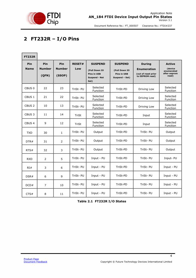
2 FT232R – I/O Pins
FT232R
Pin
Name
Pin
Number
(QFN)
Pin
Number
(SSOP)
RESET#
Low
SUSPEND
(Pull Down IO
Pins in USB
Suspend - Not
Set)
SUSPEND
(Pull Down IO
Pins in USB
Suspend – Set)
During
Enumeration
(out of reset prior
to EEPROM read)
Active
(device
enumerated
after eeprom read)
CBUS 0 22 23 TriSt- PU Selected Function
TriSt-PD Driving Low Selected Function
CBUS 1 21 22 TriSt- PU Selected Function
TriSt-PD Driving Low Selected Function
CBUS 2 10 13 TriSt- PU Selected
Function TriSt-PD Driving Low
Selected
Function
CBUS 3 11 14 TriSt Selected Function
TriSt-PD Input Selected Function
CBUS 4 9 12 TriSt Selected Function
TriSt-PD Input Selected Function
TXD 30 1 TriSt- PU Output TriSt-PD TriSt- PU Output
DTR# 31 2 TriSt- PU Output TriSt-PD TriSt- PU Output
RTS# 32 3 TriSt- PU Output TriSt-PD TriSt- PU Output
RXD 2 5 TriSt- PU Input - PU TriSt-PD TriSt- PU Input- PU
RI# 3 6 TriSt- PU Input - PU TriSt-PD TriSt- PU Input - PU
DSR# 6 9 TriSt- PU Input - PU TriSt-PD TriSt- PU Input - PU
DCD# 7 10 TriSt- PU Input - PU TriSt-PD TriSt- PU Input - PU
CTS# 8 11 TriSt- PU Input - PU TriSt-PD TriSt- PU Input - PU
Table 2.1 FT232R I/O States
Page 6
Application Note
AN_184 FTDI Device Input Output Pin States Version 3.1
Document Reference No.: FT_000507 Clearance No.: FTDI#237
5 Product Page Document Feedback Copyright © Future Technology Devices International Limited
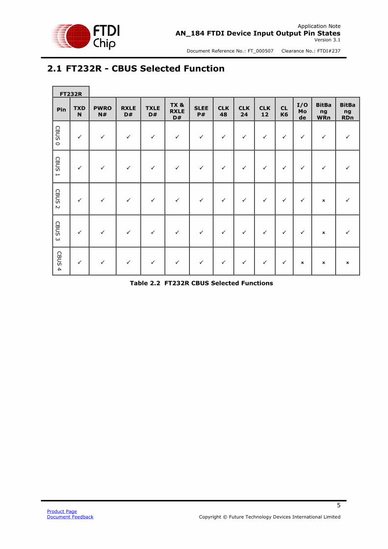
2.1 FT232R - CBUS Selected Function
FT232R
Pin TXDN
PWRON#
RXLED#
TXLED#
TX & RXLED#
SLEEP#
CLK48
CLK24
CLK12
CLK6
I/O Mode
BitBang
WRn
BitBang
RDn
CBU
S 0
CBU
S 1
CBU
S 2
CBU
S 3
CBU
S 4
Table 2.2 FT232R CBUS Selected Functions
Page 7
Application Note
AN_184 FTDI Device Input Output Pin States Version 3.1
Document Reference No.: FT_000507 Clearance No.: FTDI#237
6 Product Page Document Feedback Copyright © Future Technology Devices International Limited
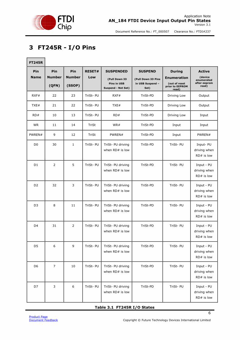
3 FT245R - I/O Pins
FT245R
Pin
Name
Pin
Number
(QFN)
Pin
Number
(SSOP)
RESET#
Low
SUSPENDED
(Pull Down IO
Pins in USB
Suspend - Not Set)
SUSPEND
(Pull Down IO Pins
in USB Suspend –
Set)
During
Enumeration
(out of reset prior to EEPROM
read)
Active
(device enumerated
after eeprom
read)
RXF# 22 23 TriSt- PU RXF# TriSt-PD Driving Low Output
TXE# 21 22 TriSt- PU TXE# TriSt-PD Driving Low Output
RD# 10 13 TriSt- PU RD# TriSt-PD Driving Low Input
WR 11 14 TriSt WR# TriSt-PD Input Input
PWREN# 9 12 TriSt PWREN# TriSt-PD Input PWREN#
D0 30 1 TriSt- PU TriSt- PU driving
when RD# is low
TriSt-PD TriSt- PU Input- PU
driving when
RD# is low
D1 2 5 TriSt- PU TriSt- PU driving
when RD# is low
TriSt-PD TriSt- PU Input - PU
driving when
RD# is low
D2 32 3 TriSt- PU TriSt- PU driving
when RD# is low
TriSt-PD TriSt- PU Input - PU
driving when
RD# is low
D3 8 11 TriSt- PU TriSt- PU driving
when RD# is low
TriSt-PD TriSt- PU Input - PU
driving when
RD# is low
D4 31 2 TriSt- PU TriSt- PU driving
when RD# is low
TriSt-PD TriSt- PU Input - PU
driving when
RD# is low
D5 6 9 TriSt- PU TriSt- PU driving
when RD# is low
TriSt-PD TriSt- PU Input - PU
driving when
RD# is low
D6 7 10 TriSt- PU TriSt- PU driving
when RD# is low
TriSt-PD TriSt- PU Input - PU
driving when
RD# is low
D7 3 6 TriSt- PU TriSt- PU driving
when RD# is low
TriSt-PD TriSt- PU Input - PU
driving when
RD# is low
Table 3.1 FT245R I/O States
Page 8
Application Note
AN_184 FTDI Device Input Output Pin States Version 3.1
Document Reference No.: FT_000507 Clearance No.: FTDI#237
7 Product Page Document Feedback Copyright © Future Technology Devices International Limited
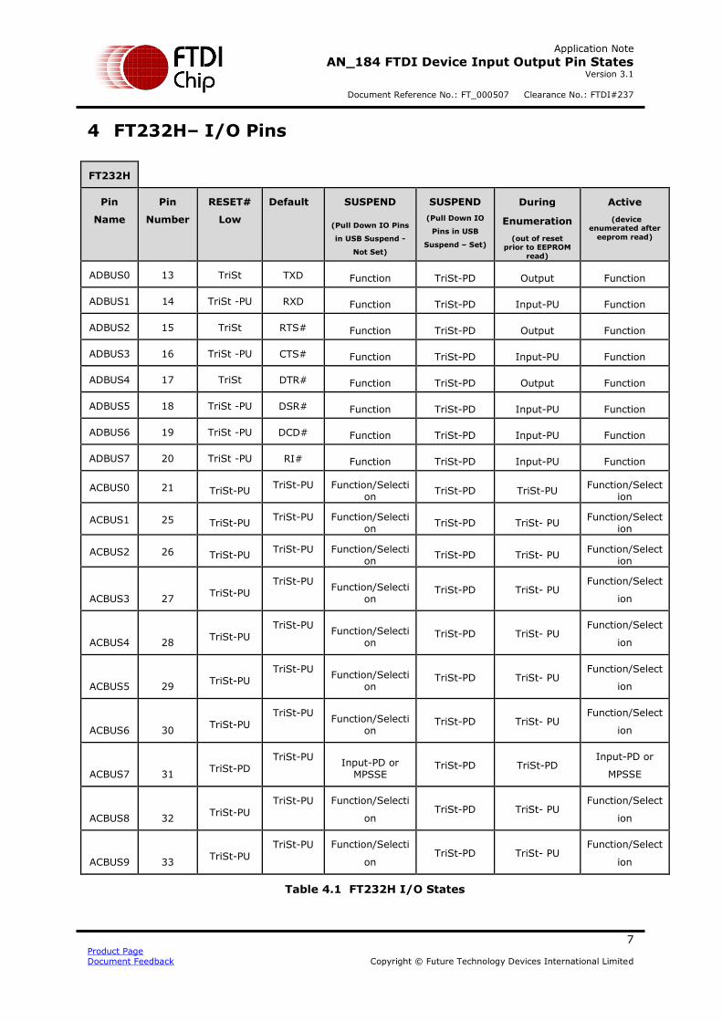
4 FT232H– I/O Pins
FT232H
Pin
Name
Pin
Number
RESET#
Low
Default SUSPEND
(Pull Down IO Pins
in USB Suspend -
Not Set)
SUSPEND
(Pull Down IO
Pins in USB
Suspend – Set)
During
Enumeration
(out of reset prior to EEPROM
read)
Active
(device enumerated after
eeprom read)
ADBUS0 13 TriSt TXD Function TriSt-PD Output Function
ADBUS1 14 TriSt -PU RXD Function TriSt-PD Input-PU Function
ADBUS2 15 TriSt RTS# Function TriSt-PD Output Function
ADBUS3 16 TriSt -PU CTS# Function TriSt-PD Input-PU Function
ADBUS4 17 TriSt DTR# Function TriSt-PD Output Function
ADBUS5 18 TriSt -PU DSR# Function TriSt-PD Input-PU Function
ADBUS6 19 TriSt -PU DCD# Function TriSt-PD Input-PU Function
ADBUS7 20 TriSt -PU RI# Function TriSt-PD Input-PU Function
ACBUS0 21 TriSt-PU TriSt-PU Function/Selecti
on TriSt-PD TriSt-PU
Function/Selection
ACBUS1 25 TriSt-PU TriSt-PU Function/Selecti
on TriSt-PD TriSt- PU
Function/Selection
ACBUS2 26 TriSt-PU TriSt-PU Function/Selecti
on TriSt-PD TriSt- PU
Function/Selection
ACBUS3 27 TriSt-PU
TriSt-PU Function/Selecti
on TriSt-PD TriSt- PU
Function/Select
ion
ACBUS4 28 TriSt-PU
TriSt-PU Function/Selecti
on TriSt-PD TriSt- PU
Function/Select
ion
ACBUS5 29 TriSt-PU
TriSt-PU Function/Selecti
on TriSt-PD TriSt- PU
Function/Select
ion
ACBUS6 30 TriSt-PU
TriSt-PU Function/Selecti
on TriSt-PD TriSt- PU
Function/Select
ion
ACBUS7 31 TriSt-PD
TriSt-PU Input-PD or
MPSSE TriSt-PD TriSt-PD
Input-PD or
MPSSE
ACBUS8 32 TriSt-PU
TriSt-PU Function/Selecti
on TriSt-PD TriSt- PU
Function/Select
ion
ACBUS9 33 TriSt-PU
TriSt-PU Function/Selecti
on TriSt-PD TriSt- PU
Function/Select
ion
Table 4.1 FT232H I/O States
Page 9
Application Note
AN_184 FTDI Device Input Output Pin States Version 3.1
Document Reference No.: FT_000507 Clearance No.: FTDI#237
8 Product Page Document Feedback Copyright © Future Technology Devices International Limited
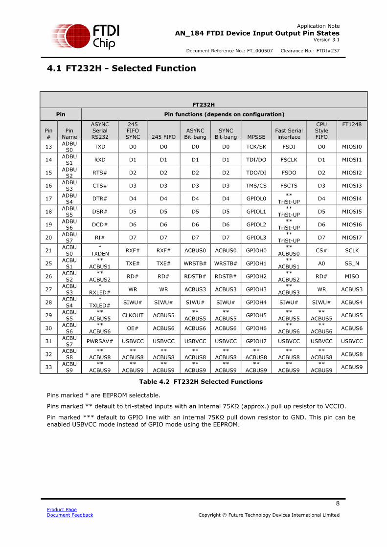
4.1 FT232H - Selected Function
Table 4.2 FT232H Selected Functions
Pins marked * are EEPROM selectable.
Pins marked ** default to tri-stated inputs with an internal 75KΩ (approx.) pull up resistor to VCCIO.
Pin marked *** default to GPIO line with an internal 75KΩ pull down resistor to GND. This pin can be enabled USBVCC mode instead of GPIO mode using the EEPROM.
FT232H
Pin Pin functions (depends on configuration)
Pin #
Pin Name
ASYNC Serial RS232
245 FIFO SYNC 245 FIFO
ASYNC Bit-bang
SYNC Bit-bang MPSSE
Fast Serial interface
CPU Style FIFO
FT1248
13 ADBU
S0 TXD D0 D0 D0 D0 TCK/SK FSDI D0 MIOSI0
14 ADBU
S1 RXD D1 D1 D1 D1 TDI/DO FSCLK D1 MIOSI1
15 ADBU
S2 RTS# D2 D2 D2 D2 TDO/DI FSDO D2 MIOSI2
16 ADBU
S3 CTS# D3 D3 D3 D3 TMS/CS FSCTS D3 MIOSI3
17 ADBU
S4 DTR# D4 D4 D4 D4 GPIOL0
** TriSt-UP
D4 MIOSI4
18 ADBU
S5 DSR# D5 D5 D5 D5 GPIOL1
** TriSt-UP
D5 MIOSI5
19 ADBU
S6 DCD# D6 D6 D6 D6 GPIOL2
** TriSt-UP
D6 MIOSI6
20 ADBU
S7 RI# D7 D7 D7 D7 GPIOL3
** TriSt-UP
D7 MIOSI7
21 ACBU
S0
*
TXDEN RXF# RXF# ACBUS0 ACBUS0 GPIOH0
**
ACBUS0 CS# SCLK
25 ACBU
S1 **
ACBUS1 TXE# TXE# WRSTB# WRSTB# GPIOH1
** ACBUS1
A0 SS_N
26 ACBU
S2 **
ACBUS2 RD# RD# RDSTB# RDSTB# GPIOH2
** ACBUS2
RD# MISO
27 ACBU
S3 *
RXLED# WR WR ACBUS3 ACBUS3 GPIOH3
** ACBUS3
WR ACBUS3
28 ACBU
S4 *
TXLED# SIWU# SIWU# SIWU# SIWU# GPIOH4 SIWU# SIWU# ACBUS4
29 ACBU
S5 **
ACBUS5 CLKOUT ACBUS5
** ACBUS5
** ACBUS5
GPIOH5 **
ACBUS5 **
ACBUS5 ACBUS5
30 ACBU
S6 **
ACBUS6 OE# ACBUS6 ACBUS6 ACBUS6 GPIOH6
** ACBUS6
** ACBUS6
ACBUS6
31 ACBU
S7 PWRSAV# USBVCC USBVCC USBVCC USBVCC GPIOH7 USBVCC USBVCC USBVCC
32 ACBU
S8 **
ACBUS8 **
ACBUS8 **
ACBUS8 **
ACBUS8 **
ACBUS8 **
ACBUS8 **
ACBUS8 **
ACBUS8 ACBUS8
33 ACBU
S9 **
ACBUS9 **
ACBUS9 **
ACBUS9 **
ACBUS9 **
ACBUS9 **
ACBUS9 **
ACBUS9 **
ACBUS9 ACBUS9
Page 10
Application Note
AN_184 FTDI Device Input Output Pin States Version 3.1
Document Reference No.: FT_000507 Clearance No.: FTDI#237
9 Product Page Document Feedback Copyright © Future Technology Devices International Limited
5 FT2232H
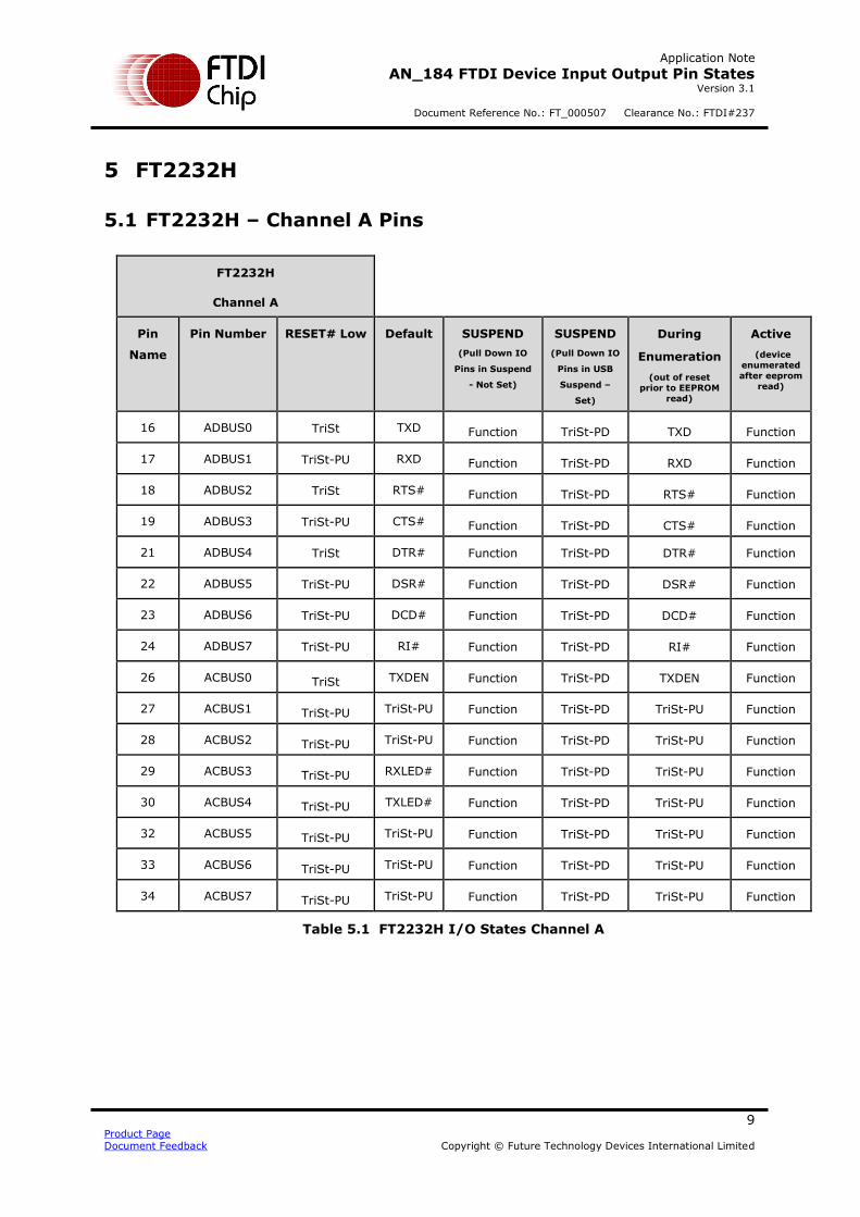
5.1 FT2232H – Channel A Pins
FT2232H
Channel A
Pin
Name
Pin Number RESET# Low Default SUSPEND
(Pull Down IO
Pins in Suspend
- Not Set)
SUSPEND
(Pull Down IO
Pins in USB
Suspend –
Set)
During
Enumeration
(out of reset
prior to EEPROM
read)
Active
(device
enumerated
after eeprom
read)
16 ADBUS0 TriSt TXD Function TriSt-PD TXD Function
17 ADBUS1 TriSt-PU RXD Function TriSt-PD RXD Function
18 ADBUS2 TriSt RTS# Function TriSt-PD RTS# Function
19 ADBUS3 TriSt-PU CTS# Function TriSt-PD CTS# Function
21 ADBUS4 TriSt DTR# Function TriSt-PD DTR# Function
22 ADBUS5 TriSt-PU DSR# Function TriSt-PD DSR# Function
23 ADBUS6 TriSt-PU DCD# Function TriSt-PD DCD# Function
24 ADBUS7 TriSt-PU RI# Function TriSt-PD RI# Function
26 ACBUS0 TriSt TXDEN Function TriSt-PD TXDEN Function
27 ACBUS1 TriSt-PU TriSt-PU Function TriSt-PD TriSt-PU Function
28 ACBUS2 TriSt-PU TriSt-PU Function TriSt-PD TriSt-PU Function
29 ACBUS3 TriSt-PU RXLED# Function TriSt-PD TriSt-PU Function
30 ACBUS4 TriSt-PU TXLED# Function TriSt-PD TriSt-PU Function
32 ACBUS5 TriSt-PU TriSt-PU Function TriSt-PD TriSt-PU Function
33 ACBUS6 TriSt-PU TriSt-PU Function TriSt-PD TriSt-PU Function
34 ACBUS7 TriSt-PU TriSt-PU Function TriSt-PD TriSt-PU Function
Table 5.1 FT2232H I/O States Channel A
Page 11
Application Note
AN_184 FTDI Device Input Output Pin States Version 3.1
Document Reference No.: FT_000507 Clearance No.: FTDI#237
10 Product Page Document Feedback Copyright © Future Technology Devices International Limited
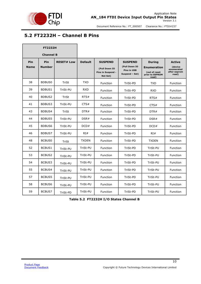
5.2 FT2232H – Channel B Pins
FT2232H
Channel B
Pin
Name
Pin
Number
RESET# Low Default SUSPEND
(Pull Down IO
Pins in Suspend -
Not Set)
SUSPEND
(Pull Down IO
Pins in USB
Suspend – Set)
During
Enumeration
(out of reset
prior to EEPROM
read)
Active
(device
enumerated
after eeprom
read)
38 BDBUS0 TriSt TXD Function TriSt-PD TXD Function
39 BDBUS1 TriSt-PU RXD Function TriSt-PD RXD Function
40 BDBUS2 TriSt RTS# Function TriSt-PD RTS# Function
41 BDBUS3 TriSt-PU CTS# Function TriSt-PD CTS# Function
43 BDBUS4 TriSt DTR# Function TriSt-PD DTR# Function
44 BDBUS5 TriSt-PU DSR# Function TriSt-PD DSR# Function
45 BDBUS6 TriSt-PU DCD# Function TriSt-PD DCD# Function
46 BDBUS7 TriSt-PU RI# Function TriSt-PD RI# Function
48 BCBUS0 TriSt TXDEN Function TriSt-PD TXDEN Function
52 BCBUS1 TriSt-PU TriSt-PU Function TriSt-PD TriSt-PU Function
53 BCBUS2 TriSt-PU TriSt-PU Function TriSt-PD TriSt-PU Function
54 BCBUS3 TriSt-PU TriSt-PU Function TriSt-PD TriSt-PU Function
55 BCBUS4 TriSt-PU TriSt-PU Function TriSt-PD TriSt-PU Function
57 BCBUS5 TriSt-PU TriSt-PU Function TriSt-PD TriSt-PU Function
58 BCBUS6 TriSt-PU TriSt-PU Function TriSt-PD TriSt-PU Function
59 BCBUS7 TriSt-PD TriSt-PU Function TriSt-PD TriSt-PU Function
Table 5.2 FT2232H I/O States Channel B
Page 12
Application Note
AN_184 FTDI Device Input Output Pin States Version 3.1
Document Reference No.: FT_000507 Clearance No.: FTDI#237
11 Product Page Document Feedback Copyright © Future Technology Devices International Limited
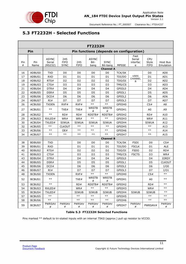
5.3 FT2232H - Selected Functions
Table 5.3 FT2232H Selected Functions
Pins marked ** default to tri-stated inputs with an internal 75KΩ (approx.) pull up resistor to VCCIO.
FT2232H
Pin Pin functions (depends on configuration)
Pin #
Pin Name
ASYNC Serial
(RS232)
245 FIFO SYNC
245 FIFO
ASYNC Bit-bang
SYNC Bit-bang MPSSE
Fast Serial
interface
CPU Style FIFO
Host Bus Emulation
Channel A
16 ADBUS0 TXD D0 D0 D0 D0 TCK/SK
USES
CHANNEL
B
D0 AD0
17 ADBUS1 RXD D1 D1 D1 D1 TDI/DO D1 AD1
18 ADBUS2 RTS# D2 D2 D2 D2 TDO/DI D2 AD2
19 ADBUS3 CTS# D3 D3 D3 D3 TMS/CS D3 AD3
21 ADBUS4 DTR# D4 D4 D4 D4 GPIOL0 D4 AD4
22 ADBUS5 DSR# D5 D5 D5 D5 GPIOL1 D5 AD5
23 ADBUS6 DCD# D6 D6 D6 D6 GPIOL2 D6 AD6
24 ADBUS7 RI# D7 D7 D7 D7 GPIOL3 D7 AD7
26 ACBUS0 TXDEN RXF# RXF# ** ** GPIOH0 CS# A8
27 ACBUS1 ** TXE# TXE# WRSTB
#
WRSTB
# GPIOH1 A0 A9
28 ACBUS2 ** RD# RD# RDSTB# RDSTB# GPIOH2 RD# A10
29 ACBUS3 RXLED# WR# WR# ** ** GPIOH3 WR# A11
30 ACBUS4 TXLED# SIWUA SIWUA SIWUA SIWUA GPIOH4 SIWUA A12
32 ACBUS5 ** CLKOUT ** ** ** GPIOH5 ** A13
33 ACBUS6 ** OE# ** ** ** GPIOH6 ** A14
34 ACBUS7 ** ** ** ** ** GPIOH7 ** A15
Channel B
38 BDBUS0 TXD D0 D0 D0 TCK/SK FSDI D0 CS#
39 BDBUS1 RXD D1 D1 D1 TDI/DO FSCLK D1 ALE
40 BDBUS2 RTS# D2 D2 D2 TDO/DI FSDO D2 RD#
41 BDBUS3 CTS# D3 D3 D3 TMS/CS FSCTS D3 WR#
43 BDBUS4 DTR# D4 D4 D4 GPIOL0 D4 IORDY
44 BDBUS5 DSR# D5 D5 D5 GPIOL1 D5 CLKOUT
45 BDBUS6 DCD# D6 D6 D6 GPIOL2 D6 I/O0
46 BDBUS7 RI# D7 D7 D7 GPIOL3 D7 I/O1
48 BCBUS0 TXDEN RXF# ** ** GPIOH0 CS# **
52 BCBUS1 ** TXE# WRSTB
# WRSTB
# GPIOH1 A0 **
53 BCBUS2 ** RD# RDSTB# RDSTB# GPIOH2 RD# **
54 BCBUS3 RXLED# WR# ** ** GPIOH3 WR# **
55 BCBUS4 TXLED# SIWUB SIWUB SIWUB GPIOH4 SIWUB SIWUB **
57 BCBUS5 ** ** ** ** GPIOH5 ** **
58 BCBUS6 ** ** ** ** GPIOH6 ** **
59 BCBUS7 PWRSAV
#
PWRSAV#
PWRSAV#
PWRSAV#
PWRSAV#
GPIOH7 PWRSAV
# PWRSAV#
PWRSAV#
Page 13
Application Note
AN_184 FTDI Device Input Output Pin States Version 3.1
Document Reference No.: FT_000507 Clearance No.: FTDI#237
12 Product Page Document Feedback Copyright © Future Technology Devices International Limited
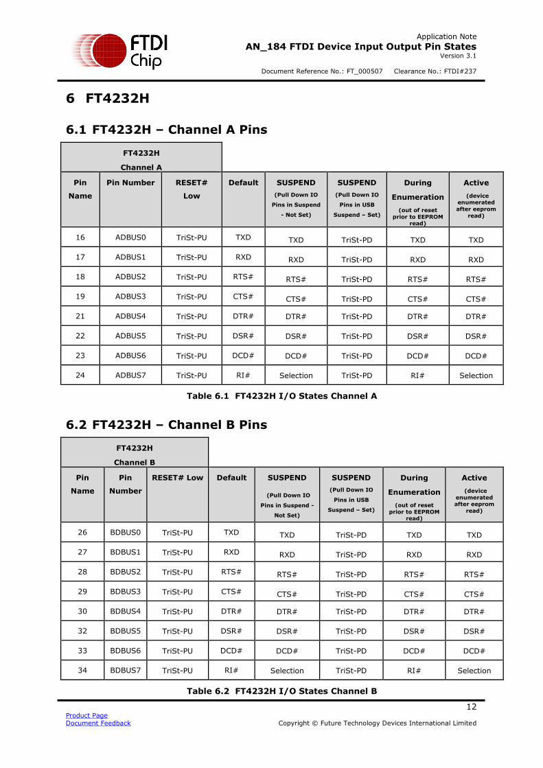
6 FT4232H
6.1 FT4232H – Channel A Pins
FT4232H
Channel A
Pin
Name
Pin Number RESET#
Low
Default SUSPEND
(Pull Down IO
Pins in Suspend
- Not Set)
SUSPEND
(Pull Down IO
Pins in USB
Suspend – Set)
During
Enumeration
(out of reset
prior to EEPROM read)
Active
(device enumerated
after eeprom
read)
16 ADBUS0 TriSt-PU TXD TXD TriSt-PD TXD TXD
17 ADBUS1 TriSt-PU RXD RXD TriSt-PD RXD RXD
18 ADBUS2 TriSt-PU RTS# RTS# TriSt-PD RTS# RTS#
19 ADBUS3 TriSt-PU CTS# CTS# TriSt-PD CTS# CTS#
21 ADBUS4 TriSt-PU DTR# DTR# TriSt-PD DTR# DTR#
22 ADBUS5 TriSt-PU DSR# DSR# TriSt-PD DSR# DSR#
23 ADBUS6 TriSt-PU DCD# DCD# TriSt-PD DCD# DCD#
24 ADBUS7 TriSt-PU RI# Selection TriSt-PD RI# Selection
Table 6.1 FT4232H I/O States Channel A
6.2 FT4232H – Channel B Pins
FT4232H
Channel B
Pin
Name
Pin
Number
RESET# Low Default SUSPEND
(Pull Down IO
Pins in Suspend -
Not Set)
SUSPEND
(Pull Down IO
Pins in USB
Suspend – Set)
During
Enumeration
(out of reset
prior to EEPROM read)
Active
(device
enumerated after eeprom
read)
26 BDBUS0 TriSt-PU TXD TXD TriSt-PD TXD TXD
27 BDBUS1 TriSt-PU RXD RXD TriSt-PD RXD RXD
28 BDBUS2 TriSt-PU RTS# RTS# TriSt-PD RTS# RTS#
29 BDBUS3 TriSt-PU CTS# CTS# TriSt-PD CTS# CTS#
30 BDBUS4 TriSt-PU DTR# DTR# TriSt-PD DTR# DTR#
32 BDBUS5 TriSt-PU DSR# DSR# TriSt-PD DSR# DSR#
33 BDBUS6 TriSt-PU DCD# DCD# TriSt-PD DCD# DCD#
34 BDBUS7 TriSt-PU RI# Selection TriSt-PD RI# Selection
Table 6.2 FT4232H I/O States Channel B
Page 14
Application Note
AN_184 FTDI Device Input Output Pin States Version 3.1
Document Reference No.: FT_000507 Clearance No.: FTDI#237
13 Product Page Document Feedback Copyright © Future Technology Devices International Limited
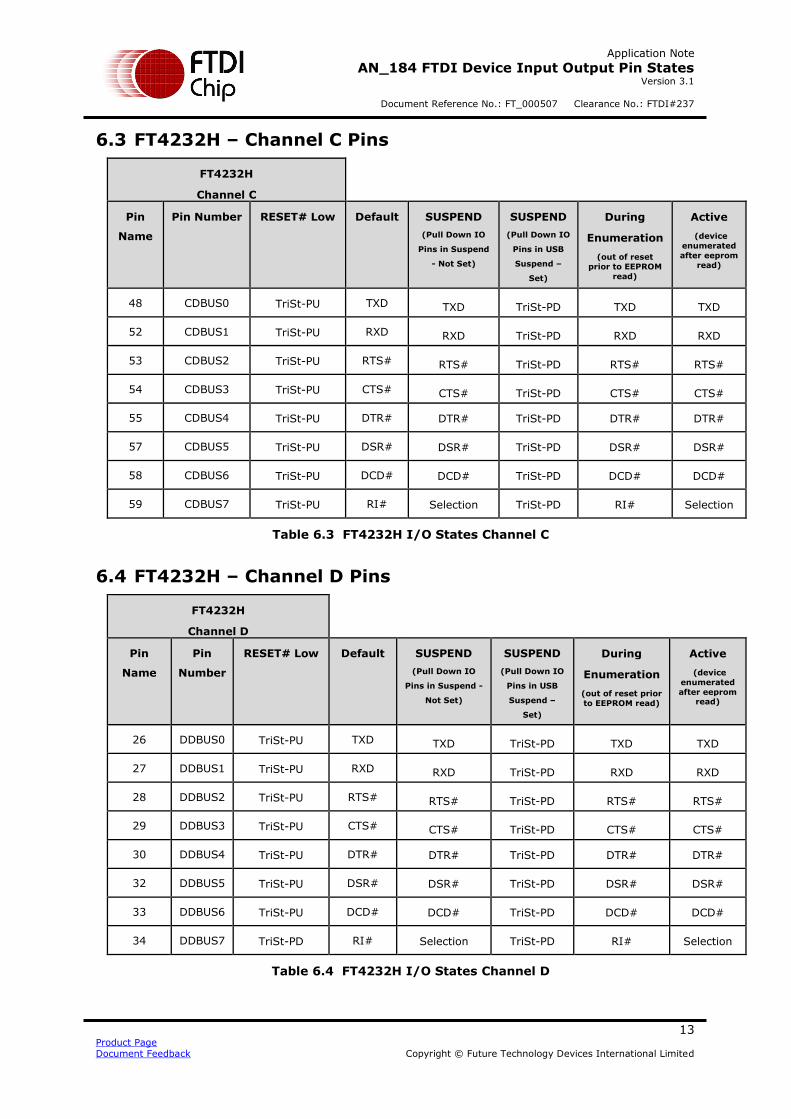
6.3 FT4232H – Channel C Pins
FT4232H
Channel C
Pin
Name
Pin Number RESET# Low Default SUSPEND
(Pull Down IO
Pins in Suspend
- Not Set)
SUSPEND
(Pull Down IO
Pins in USB
Suspend –
Set)
During
Enumeration
(out of reset
prior to EEPROM
read)
Active
(device
enumerated
after eeprom
read)
48 CDBUS0 TriSt-PU TXD TXD TriSt-PD TXD TXD
52 CDBUS1 TriSt-PU RXD RXD TriSt-PD RXD RXD
53 CDBUS2 TriSt-PU RTS# RTS# TriSt-PD RTS# RTS#
54 CDBUS3 TriSt-PU CTS# CTS# TriSt-PD CTS# CTS#
55 CDBUS4 TriSt-PU DTR# DTR# TriSt-PD DTR# DTR#
57 CDBUS5 TriSt-PU DSR# DSR# TriSt-PD DSR# DSR#
58 CDBUS6 TriSt-PU DCD# DCD# TriSt-PD DCD# DCD#
59 CDBUS7 TriSt-PU RI# Selection TriSt-PD RI# Selection
Table 6.3 FT4232H I/O States Channel C
6.4 FT4232H – Channel D Pins
FT4232H
Channel D
Pin
Name
Pin
Number
RESET# Low Default SUSPEND
(Pull Down IO
Pins in Suspend -
Not Set)
SUSPEND
(Pull Down IO
Pins in USB
Suspend –
Set)
During
Enumeration
(out of reset prior
to EEPROM read)
Active
(device
enumerated
after eeprom read)
26 DDBUS0 TriSt-PU TXD TXD TriSt-PD TXD TXD
27 DDBUS1 TriSt-PU RXD RXD TriSt-PD RXD RXD
28 DDBUS2 TriSt-PU RTS# RTS# TriSt-PD RTS# RTS#
29 DDBUS3 TriSt-PU CTS# CTS# TriSt-PD CTS# CTS#
30 DDBUS4 TriSt-PU DTR# DTR# TriSt-PD DTR# DTR#
32 DDBUS5 TriSt-PU DSR# DSR# TriSt-PD DSR# DSR#
33 DDBUS6 TriSt-PU DCD# DCD# TriSt-PD DCD# DCD#
34 DDBUS7 TriSt-PD RI# Selection TriSt-PD RI# Selection
Table 6.4 FT4232H I/O States Channel D
Page 15
Application Note
AN_184 FTDI Device Input Output Pin States Version 3.1
Document Reference No.: FT_000507 Clearance No.: FTDI#237
14 Product Page Document Feedback Copyright © Future Technology Devices International Limited
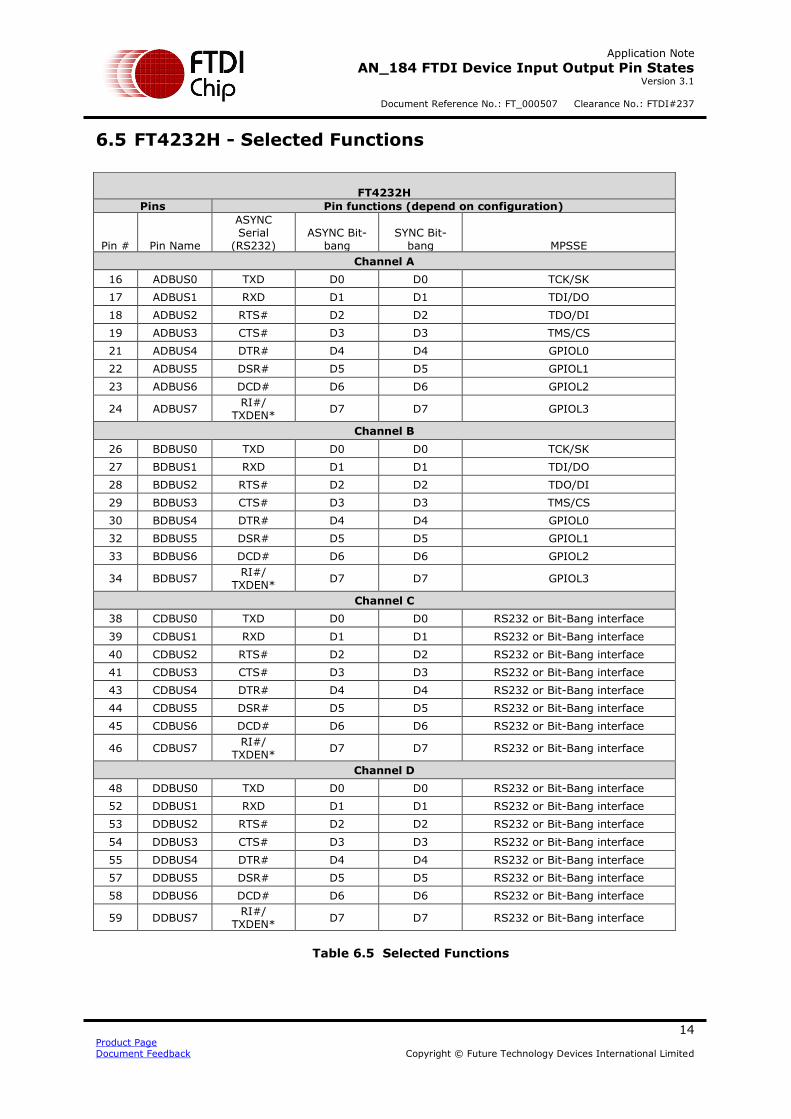
6.5 FT4232H - Selected Functions
Table 6.5 Selected Functions
FT4232H
Pins Pin functions (depend on configuration)
Pin # Pin Name
ASYNC Serial
(RS232) ASYNC Bit-
bang SYNC Bit-
bang MPSSE
Channel A
16 ADBUS0 TXD D0 D0 TCK/SK
17 ADBUS1 RXD D1 D1 TDI/DO
18 ADBUS2 RTS# D2 D2 TDO/DI
19 ADBUS3 CTS# D3 D3 TMS/CS
21 ADBUS4 DTR# D4 D4 GPIOL0
22 ADBUS5 DSR# D5 D5 GPIOL1
23 ADBUS6 DCD# D6 D6 GPIOL2
24 ADBUS7 RI#/
TXDEN* D7 D7 GPIOL3
Channel B
26 BDBUS0 TXD D0 D0 TCK/SK
27 BDBUS1 RXD D1 D1 TDI/DO
28 BDBUS2 RTS# D2 D2 TDO/DI
29 BDBUS3 CTS# D3 D3 TMS/CS
30 BDBUS4 DTR# D4 D4 GPIOL0
32 BDBUS5 DSR# D5 D5 GPIOL1
33 BDBUS6 DCD# D6 D6 GPIOL2
34 BDBUS7 RI#/
TXDEN* D7 D7 GPIOL3
Channel C
38 CDBUS0 TXD D0 D0 RS232 or Bit-Bang interface
39 CDBUS1 RXD D1 D1 RS232 or Bit-Bang interface
40 CDBUS2 RTS# D2 D2 RS232 or Bit-Bang interface
41 CDBUS3 CTS# D3 D3 RS232 or Bit-Bang interface
43 CDBUS4 DTR# D4 D4 RS232 or Bit-Bang interface
44 CDBUS5 DSR# D5 D5 RS232 or Bit-Bang interface
45 CDBUS6 DCD# D6 D6 RS232 or Bit-Bang interface
46 CDBUS7 RI#/
TXDEN* D7 D7 RS232 or Bit-Bang interface
Channel D
48 DDBUS0 TXD D0 D0 RS232 or Bit-Bang interface
52 DDBUS1 RXD D1 D1 RS232 or Bit-Bang interface
53 DDBUS2 RTS# D2 D2 RS232 or Bit-Bang interface
54 DDBUS3 CTS# D3 D3 RS232 or Bit-Bang interface
55 DDBUS4 DTR# D4 D4 RS232 or Bit-Bang interface
57 DDBUS5 DSR# D5 D5 RS232 or Bit-Bang interface
58 DDBUS6 DCD# D6 D6 RS232 or Bit-Bang interface
59 DDBUS7 RI#/
TXDEN* D7 D7 RS232 or Bit-Bang interface
Page 16
Application Note
AN_184 FTDI Device Input Output Pin States Version 3.1
Document Reference No.: FT_000507 Clearance No.: FTDI#237
15 Product Page Document Feedback Copyright © Future Technology Devices International Limited
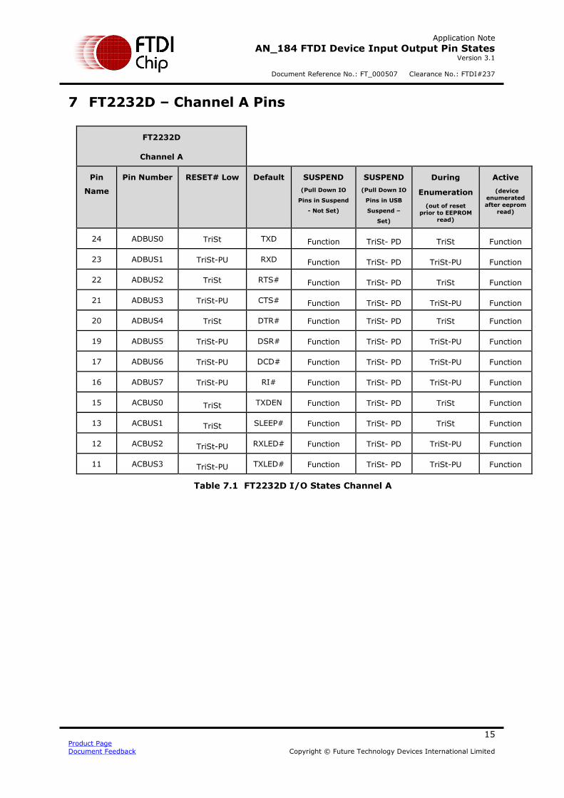
7 FT2232D – Channel A Pins
FT2232D
Channel A
Pin
Name
Pin Number RESET# Low Default SUSPEND
(Pull Down IO
Pins in Suspend
- Not Set)
SUSPEND
(Pull Down IO
Pins in USB
Suspend –
Set)
During
Enumeration
(out of reset
prior to EEPROM
read)
Active
(device
enumerated
after eeprom
read)
24 ADBUS0 TriSt TXD Function TriSt- PD TriSt Function
23 ADBUS1 TriSt-PU RXD Function TriSt- PD TriSt-PU Function
22 ADBUS2 TriSt RTS# Function TriSt- PD TriSt Function
21 ADBUS3 TriSt-PU CTS# Function TriSt- PD TriSt-PU Function
20 ADBUS4 TriSt DTR# Function TriSt- PD TriSt Function
19 ADBUS5 TriSt-PU DSR# Function TriSt- PD TriSt-PU Function
17 ADBUS6 TriSt-PU DCD# Function TriSt- PD TriSt-PU Function
16 ADBUS7 TriSt-PU RI# Function TriSt- PD TriSt-PU Function
15 ACBUS0 TriSt TXDEN Function TriSt- PD TriSt Function
13 ACBUS1 TriSt SLEEP# Function TriSt- PD TriSt Function
12 ACBUS2 TriSt-PU RXLED# Function TriSt- PD TriSt-PU Function
11 ACBUS3 TriSt-PU TXLED# Function TriSt- PD TriSt-PU Function
Table 7.1 FT2232D I/O States Channel A
Page 17
Application Note
AN_184 FTDI Device Input Output Pin States Version 3.1
Document Reference No.: FT_000507 Clearance No.: FTDI#237
16 Product Page Document Feedback Copyright © Future Technology Devices International Limited
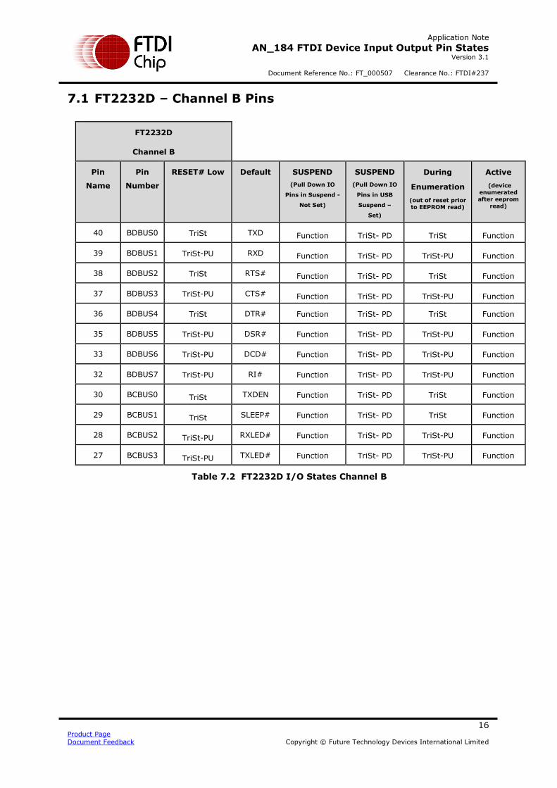
7.1 FT2232D – Channel B Pins
FT2232D
Channel B
Pin
Name
Pin
Number
RESET# Low Default SUSPEND
(Pull Down IO
Pins in Suspend -
Not Set)
SUSPEND
(Pull Down IO
Pins in USB
Suspend –
Set)
During
Enumeration
(out of reset prior
to EEPROM read)
Active
(device
enumerated
after eeprom
read)
40 BDBUS0 TriSt TXD Function TriSt- PD TriSt Function
39 BDBUS1 TriSt-PU RXD Function TriSt- PD TriSt-PU Function
38 BDBUS2 TriSt RTS# Function TriSt- PD TriSt Function
37 BDBUS3 TriSt-PU CTS# Function TriSt- PD TriSt-PU Function
36 BDBUS4 TriSt DTR# Function TriSt- PD TriSt Function
35 BDBUS5 TriSt-PU DSR# Function TriSt- PD TriSt-PU Function
33 BDBUS6 TriSt-PU DCD# Function TriSt- PD TriSt-PU Function
32 BDBUS7 TriSt-PU RI# Function TriSt- PD TriSt-PU Function
30 BCBUS0 TriSt TXDEN Function TriSt- PD TriSt Function
29 BCBUS1 TriSt SLEEP# Function TriSt- PD TriSt Function
28 BCBUS2 TriSt-PU RXLED# Function TriSt- PD TriSt-PU Function
27 BCBUS3 TriSt-PU TXLED# Function TriSt- PD TriSt-PU Function
Table 7.2 FT2232D I/O States Channel B
Page 18
Application Note
AN_184 FTDI Device Input Output Pin States Version 3.1
Document Reference No.: FT_000507 Clearance No.: FTDI#237
17 Product Page Document Feedback Copyright © Future Technology Devices International Limited
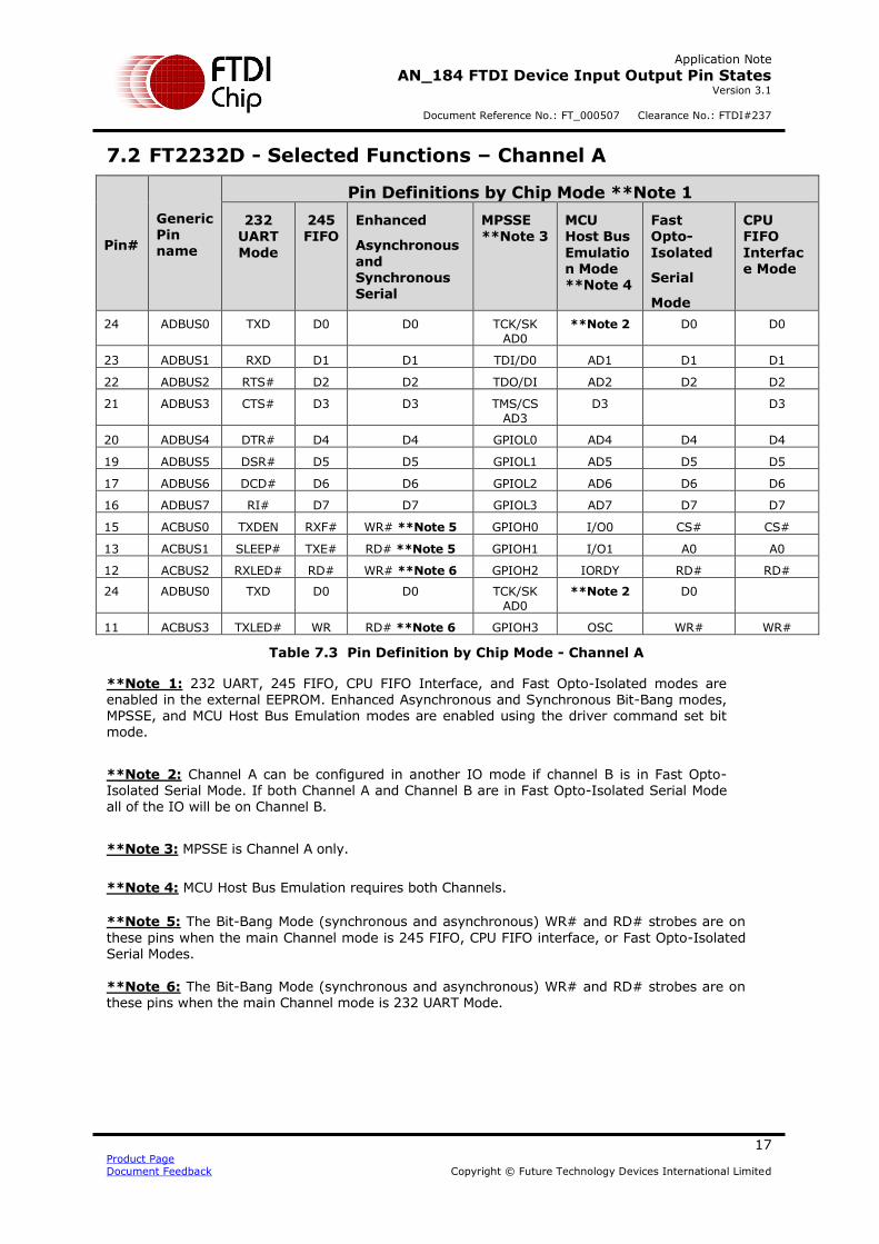
7.2 FT2232D - Selected Functions – Channel A
Pin#
Generic Pin name
Pin Definitions by Chip Mode **Note 1
232 UART
Mode
245 FIFO
Enhanced
Asynchronous
and Synchronous Serial
MPSSE **Note 3
MCU Host Bus
Emulation Mode **Note 4
Fast Opto-
Isolated
Serial
Mode
CPU FIFO
Interface Mode
24 ADBUS0 TXD D0 D0 TCK/SK
AD0
**Note 2 D0 D0
23 ADBUS1 RXD D1 D1 TDI/D0 AD1 D1 D1
22 ADBUS2 RTS# D2 D2 TDO/DI AD2 D2 D2
21 ADBUS3 CTS# D3 D3 TMS/CS
AD3
D3 D3
20 ADBUS4 DTR# D4 D4 GPIOL0 AD4 D4 D4
19 ADBUS5 DSR# D5 D5 GPIOL1 AD5 D5 D5
17 ADBUS6 DCD# D6 D6 GPIOL2 AD6 D6 D6
16 ADBUS7 RI# D7 D7 GPIOL3 AD7 D7 D7
15 ACBUS0 TXDEN RXF# WR# **Note 5 GPIOH0 I/O0 CS# CS#
13 ACBUS1 SLEEP# TXE# RD# **Note 5 GPIOH1 I/O1 A0 A0
12 ACBUS2 RXLED# RD# WR# **Note 6 GPIOH2 IORDY RD# RD#
24 ADBUS0 TXD D0 D0 TCK/SK
AD0
**Note 2 D0
11 ACBUS3 TXLED# WR RD# **Note 6 GPIOH3 OSC WR# WR#
Table 7.3 Pin Definition by Chip Mode - Channel A
**Note 1: 232 UART, 245 FIFO, CPU FIFO Interface, and Fast Opto-Isolated modes are enabled in the external EEPROM. Enhanced Asynchronous and Synchronous Bit-Bang modes, MPSSE, and MCU Host Bus Emulation modes are enabled using the driver command set bit mode.
**Note 2: Channel A can be configured in another IO mode if channel B is in Fast Opto-Isolated Serial Mode. If both Channel A and Channel B are in Fast Opto-Isolated Serial Mode all of the IO will be on Channel B.
**Note 3: MPSSE is Channel A only.
**Note 4: MCU Host Bus Emulation requires both Channels.
**Note 5: The Bit-Bang Mode (synchronous and asynchronous) WR# and RD# strobes are on
these pins when the main Channel mode is 245 FIFO, CPU FIFO interface, or Fast Opto-Isolated
Serial Modes.
**Note 6: The Bit-Bang Mode (synchronous and asynchronous) WR# and RD# strobes are on these pins when the main Channel mode is 232 UART Mode.
Page 19
Application Note
AN_184 FTDI Device Input Output Pin States Version 3.1
Document Reference No.: FT_000507 Clearance No.: FTDI#237
18 Product Page Document Feedback Copyright © Future Technology Devices International Limited
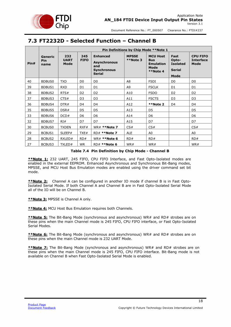
7.3 FT2232D - Selected Function – Channel B
Pin#
Generic Pin name
Pin Definitions by Chip Mode **Note 1
232 UART Mode
245 FIFO
Enhanced
Asynchronous and Synchronous Serial
MPSSE **Note 3
MCU Host Bus Emulation Mode **Note 4
Fast Opto-Isolated
Serial
Mode
CPU FIFO Interface Mode
40 BDBUS0 TXD D0 D0 A8 FSDI D0 D0
39 BDBUS1 RXD D1 D1 A9 FSCLK D1 D1
38 BDBUS2 RTS# D2 D2 A10 FSDO D2 D2
37 BDBUS3 CTS# D3 D3 A11 FSCTS D3 D3
36 BDBUS4 DTR# D4 D4 A12 **Note 2 D4 D4
35 BDBUS5 DSR# D5 D5 A13 D5 D5
33 BDBUS6 DCD# D6 D6 A14 D6 D6
32 BDBUS7 RI# D7 D7 A15 D7 D7
30 BCBUS0 TXDEN RXF# WR# **Note 7 CS# CS# CS#
29 BCBUS1 SLEEP# TXE# RD# **Note 7 ALE A0 A0
28 BCBUS2 RXLED# RD# WR# **Note 6 RD# RD# RD#
27 BCBUS3 TXLED# WR RD# **Note 6 WR# WR# WR#
Table 7.4 Pin Definition by Chip Mode - Channel B
**Note 1: 232 UART, 245 FIFO, CPU FIFO Interface, and Fast Opto-Isolated modes are enabled in the external EEPROM. Enhanced Asynchronous and Synchronous Bit-Bang modes, MPSSE, and MCU Host Bus Emulation modes are enabled using the driver command set bit
mode.
**Note 2: Channel A can be configured in another IO mode if channel B is in Fast Opto-
Isolated Serial Mode. If both Channel A and Channel B are in Fast Opto-Isolated Serial Mode all of the IO will be on Channel B.
**Note 3: MPSSE is Channel A only.
**Note 4: MCU Host Bus Emulation requires both Channels.
**Note 5: The Bit-Bang Mode (synchronous and asynchronous) WR# and RD# strobes are on
these pins when the main Channel mode is 245 FIFO, CPU FIFO interface, or Fast Opto-Isolated Serial Modes.
**Note 6: The Bit-Bang Mode (synchronous and asynchronous) WR# and RD# strobes are on
these pins when the main Channel mode is 232 UART Mode.
**Note 7: The Bit-Bang Mode (synchronous and asynchronous) WR# and RD# strobes are on
these pins when the main Channel mode is 245 FIFO, CPU FIFO interface. Bit-Bang mode is not available on Channel B when Fast Opto-Isolated Serial Mode is enabled.
Page 20
Application Note
AN_184 FTDI Device Input Output Pin States Version 3.1
Document Reference No.: FT_000507 Clearance No.: FTDI#237
19 Product Page Document Feedback Copyright © Future Technology Devices International Limited
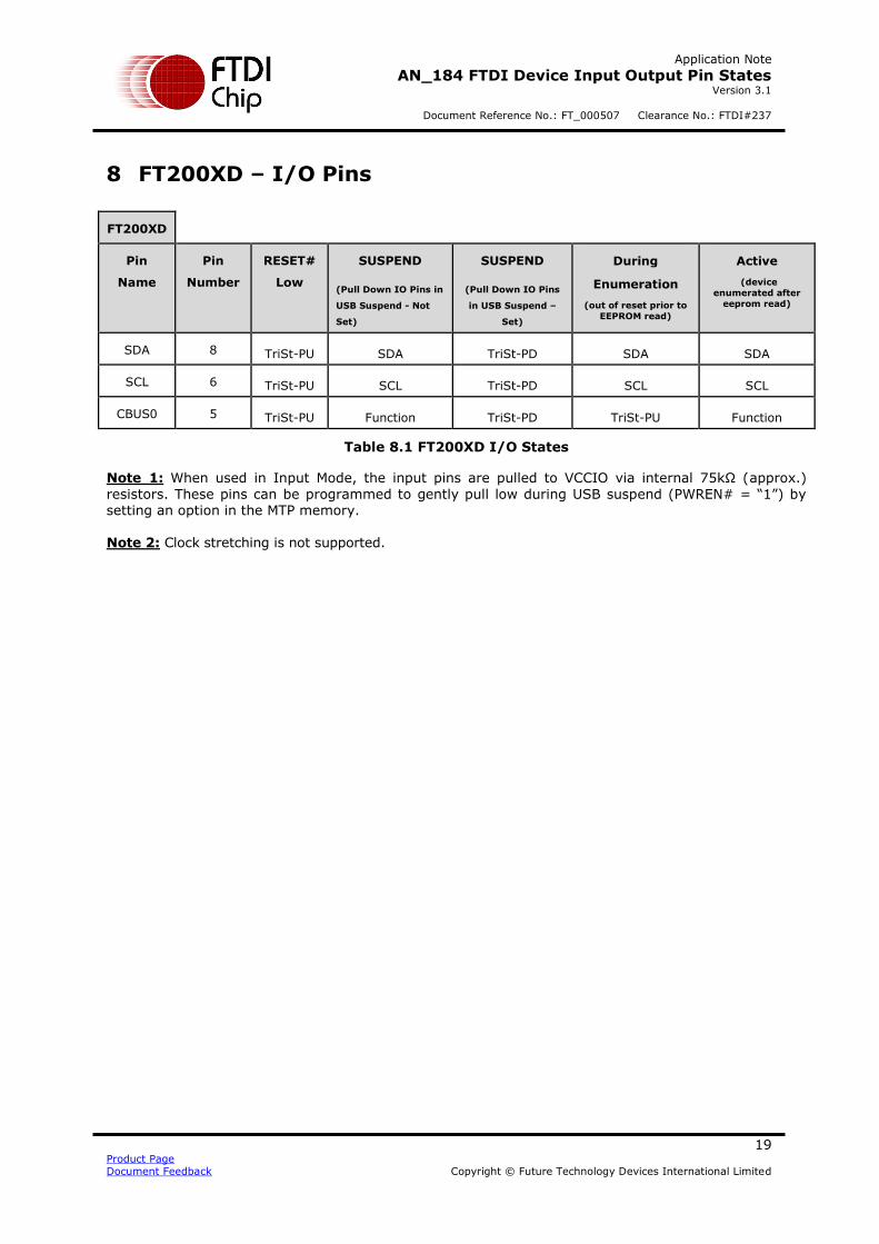
8 FT200XD – I/O Pins
FT200XD
Pin
Name
Pin
Number
RESET#
Low
SUSPEND
(Pull Down IO Pins in
USB Suspend - Not
Set)
SUSPEND
(Pull Down IO Pins
in USB Suspend –
Set)
During
Enumeration
(out of reset prior to
EEPROM read)
Active
(device
enumerated after
eeprom read)
SDA 8 TriSt-PU SDA TriSt-PD SDA SDA
SCL 6 TriSt-PU SCL TriSt-PD SCL SCL
CBUS0 5 TriSt-PU Function TriSt-PD TriSt-PU Function
Table 8.1 FT200XD I/O States
Note 1: When used in Input Mode, the input pins are pulled to VCCIO via internal 75kΩ (approx.)
resistors. These pins can be programmed to gently pull low during USB suspend (PWREN# = “1”) by setting an option in the MTP memory. Note 2: Clock stretching is not supported.
Page 21
Application Note
AN_184 FTDI Device Input Output Pin States Version 3.1
Document Reference No.: FT_000507 Clearance No.: FTDI#237
20 Product Page Document Feedback Copyright © Future Technology Devices International Limited
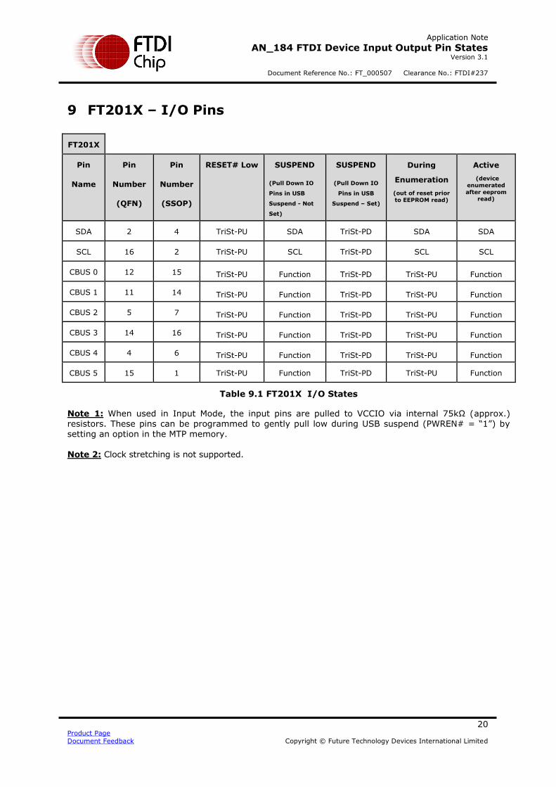
9 FT201X – I/O Pins
FT201X
Pin
Name
Pin
Number
(QFN)
Pin
Number
(SSOP)
RESET# Low SUSPEND
(Pull Down IO
Pins in USB
Suspend - Not
Set)
SUSPEND
(Pull Down IO
Pins in USB
Suspend – Set)
During
Enumeration
(out of reset prior
to EEPROM read)
Active
(device
enumerated
after eeprom read)
SDA 2 4 TriSt-PU SDA TriSt-PD SDA SDA
SCL 16 2 TriSt-PU SCL TriSt-PD SCL SCL
CBUS 0 12 15 TriSt-PU Function TriSt-PD TriSt-PU Function
CBUS 1 11 14 TriSt-PU Function TriSt-PD TriSt-PU Function
CBUS 2 5 7 TriSt-PU Function TriSt-PD TriSt-PU Function
CBUS 3 14 16 TriSt-PU Function TriSt-PD TriSt-PU Function
CBUS 4 4 6 TriSt-PU Function TriSt-PD TriSt-PU Function
CBUS 5 15 1 TriSt-PU Function TriSt-PD TriSt-PU Function
Table 9.1 FT201X I/O States
Note 1: When used in Input Mode, the input pins are pulled to VCCIO via internal 75kΩ (approx.) resistors. These pins can be programmed to gently pull low during USB suspend (PWREN# = “1”) by
setting an option in the MTP memory. Note 2: Clock stretching is not supported.
Page 22
Application Note
AN_184 FTDI Device Input Output Pin States Version 3.1
Document Reference No.: FT_000507 Clearance No.: FTDI#237
21 Product Page Document Feedback Copyright © Future Technology Devices International Limited
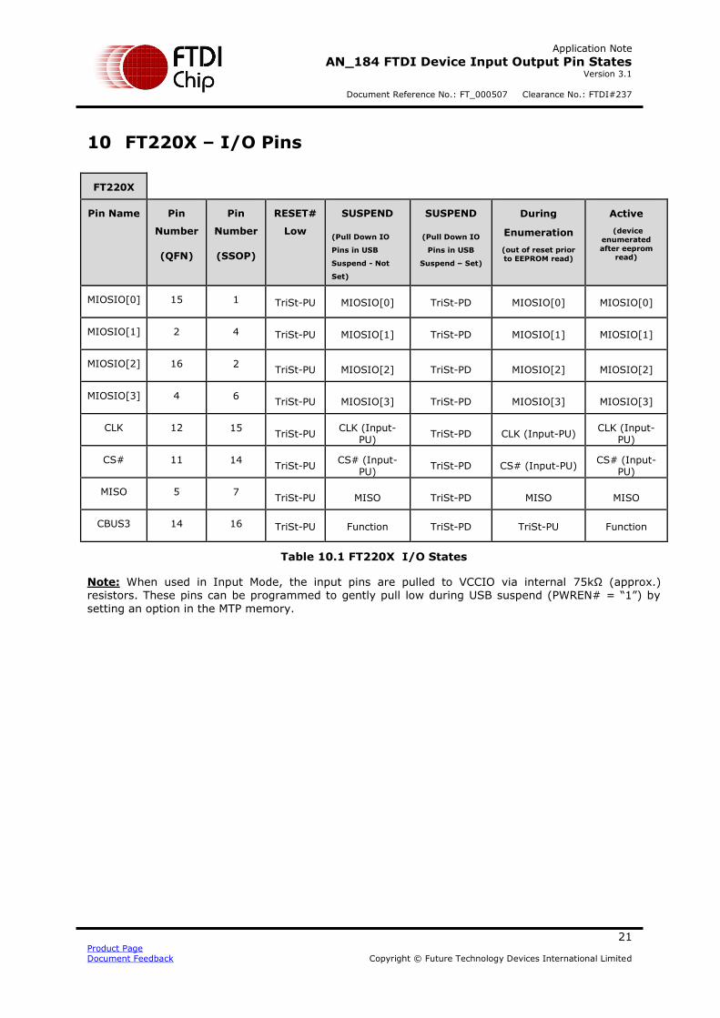
10 FT220X – I/O Pins
FT220X
Pin Name Pin
Number
(QFN)
Pin
Number
(SSOP)
RESET#
Low
SUSPEND
(Pull Down IO
Pins in USB
Suspend - Not
Set)
SUSPEND
(Pull Down IO
Pins in USB
Suspend – Set)
During
Enumeration
(out of reset prior
to EEPROM read)
Active
(device
enumerated
after eeprom read)
MIOSIO[0] 15 1 TriSt-PU MIOSIO[0] TriSt-PD MIOSIO[0] MIOSIO[0]
MIOSIO[1] 2 4 TriSt-PU MIOSIO[1] TriSt-PD MIOSIO[1] MIOSIO[1]
MIOSIO[2] 16 2 TriSt-PU MIOSIO[2] TriSt-PD MIOSIO[2] MIOSIO[2]
MIOSIO[3] 4 6 TriSt-PU MIOSIO[3] TriSt-PD MIOSIO[3] MIOSIO[3]
CLK 12 15 TriSt-PU
CLK (Input-PU)
TriSt-PD CLK (Input-PU) CLK (Input-
PU)
CS# 11 14 TriSt-PU
CS# (Input-PU)
TriSt-PD CS# (Input-PU) CS# (Input-
PU)
MISO 5 7 TriSt-PU MISO TriSt-PD MISO MISO
CBUS3 14 16 TriSt-PU Function TriSt-PD TriSt-PU Function
Table 10.1 FT220X I/O States
Note: When used in Input Mode, the input pins are pulled to VCCIO via internal 75kΩ (approx.) resistors. These pins can be programmed to gently pull low during USB suspend (PWREN# = “1”) by
setting an option in the MTP memory.
Page 23
Application Note
AN_184 FTDI Device Input Output Pin States Version 3.1
Document Reference No.: FT_000507 Clearance No.: FTDI#237
22 Product Page Document Feedback Copyright © Future Technology Devices International Limited
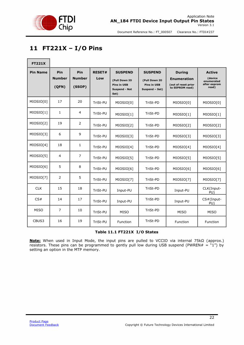
11 FT221X – I/O Pins
FT221X
Pin Name Pin
Number
(QFN)
Pin
Number
(SSOP)
RESET#
Low
SUSPEND
(Pull Down IO
Pins in USB
Suspend - Not
Set)
SUSPEND
(Pull Down IO
Pins in USB
Suspend – Set)
During
Enumeration
(out of reset prior
to EEPROM read)
Active
(device
enumerated
after eeprom read)
MIOSIO[0] 17 20 TriSt-PU MIOSIO[0] TriSt-PD MIOSIO[0] MIOSIO[0]
MIOSIO[1] 1 4 TriSt-PU MIOSIO[1] TriSt-PD MIOSIO[1] MIOSIO[1]
MIOSIO[2] 19 2 TriSt-PU MIOSIO[2] TriSt-PD MIOSIO[2] MIOSIO[2]
MIOSIO[3] 6 9 TriSt-PU MIOSIO[3] TriSt-PD MIOSIO[3] MIOSIO[3]
MIOSIO[4] 18 1 TriSt-PU MIOSIO[4] TriSt-PD MIOSIO[4] MIOSIO[4]
MIOSIO[5] 4 7 TriSt-PU MIOSIO[5] TriSt-PD MIOSIO[5] MIOSIO[5]
MIOSIO[6] 5 8 TriSt-PU MIOSIO[6] TriSt-PD MIOSIO[6] MIOSIO[6]
MIOSIO[7] 2 5 TriSt-PU MIOSIO[7] TriSt-PD MIOSIO[7] MIOSIO[7]
CLK 15 18 TriSt-PU Input-PU
TriSt-PD Input-PU
CLK(Input-PU)
CS# 14 17 TriSt-PU Input-PU
TriSt-PD Input-PU
CS#(Input-PU)
MISO 7 10 TriSt-PU MISO
TriSt-PD MISO MISO
CBUS3 16 19 TriSt-PU Function TriSt-PD Function Function
Table 11.1 FT221X I/O States
Note: When used in Input Mode, the input pins are pulled to VCCIO via internal 75kΩ (approx.) resistors. These pins can be programmed to gently pull low during USB suspend (PWREN# = “1”) by setting an option in the MTP memory.
Page 24
Application Note
AN_184 FTDI Device Input Output Pin States Version 3.1
Document Reference No.: FT_000507 Clearance No.: FTDI#237
23 Product Page Document Feedback Copyright © Future Technology Devices International Limited
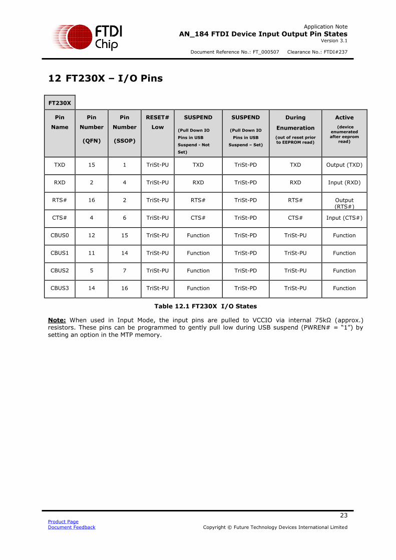
12 FT230X – I/O Pins
FT230X
Pin
Name
Pin
Number
(QFN)
Pin
Number
(SSOP)
RESET#
Low
SUSPEND
(Pull Down IO
Pins in USB
Suspend - Not
Set)
SUSPEND
(Pull Down IO
Pins in USB
Suspend – Set)
During
Enumeration
(out of reset prior
to EEPROM read)
Active
(device
enumerated
after eeprom read)
TXD 15 1 TriSt-PU TXD TriSt-PD TXD Output (TXD)
RXD 2 4 TriSt-PU RXD TriSt-PD RXD Input (RXD)
RTS# 16 2 TriSt-PU RTS# TriSt-PD RTS# Output (RTS#)
CTS# 4 6 TriSt-PU CTS# TriSt-PD CTS# Input (CTS#)
CBUS0 12 15 TriSt-PU Function TriSt-PD TriSt-PU Function
CBUS1 11 14 TriSt-PU Function TriSt-PD TriSt-PU Function
CBUS2 5 7 TriSt-PU Function TriSt-PD TriSt-PU Function
CBUS3 14 16 TriSt-PU Function TriSt-PD TriSt-PU Function
Table 12.1 FT230X I/O States
Note: When used in Input Mode, the input pins are pulled to VCCIO via internal 75kΩ (approx.) resistors. These pins can be programmed to gently pull low during USB suspend (PWREN# = “1”) by
setting an option in the MTP memory.
Page 25
Application Note
AN_184 FTDI Device Input Output Pin States Version 3.1
Document Reference No.: FT_000507 Clearance No.: FTDI#237
24 Product Page Document Feedback Copyright © Future Technology Devices International Limited
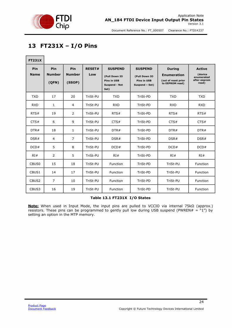
13 FT231X – I/O Pins
FT231X
Pin
Name
Pin
Number
(QFN)
Pin
Number
(SSOP)
RESET#
Low
SUSPEND
(Pull Down IO
Pins in USB
Suspend - Not
Set)
SUSPEND
(Pull Down IO
Pins in USB
Suspend – Set)
During
Enumeration
(out of reset prior
to EEPROM read)
Active
(device
enumerated
after eeprom read)
TXD 17 20 TriSt-PU TXD TriSt-PD TXD TXD
RXD 1 4 TriSt-PU RXD TriSt-PD RXD RXD
RTS# 19 2 TriSt-PU RTS# TriSt-PD RTS# RTS#
CTS# 6 9 TriSt-PU CTS# TriSt-PD CTS# CTS#
DTR# 18 1 TriSt-PU DTR# TriSt-PD DTR# DTR#
DSR# 4 7 TriSt-PU DSR# TriSt-PD DSR# DSR#
DCD# 5 8 TriSt-PU DCD# TriSt-PD DCD# DCD#
RI# 2 5 TriSt-PU RI# TriSt-PD RI# RI#
CBUS0 15 18 TriSt-PU Function TriSt-PD TriSt-PU Function
CBUS1 14 17 TriSt-PU Function TriSt-PD TriSt-PU Function
CBUS2 7 10 TriSt-PU Function TriSt-PD TriSt-PU Function
CBUS3 16 19 TriSt-PU Function TriSt-PD TriSt-PU Function
Table 13.1 FT231X I/O States
Note: When used in Input Mode, the input pins are pulled to VCCIO via internal 75kΩ (approx.)
resistors. These pins can be programmed to gently pull low during USB suspend (PWREN# = “1”) by setting an option in the MTP memory.
Page 26
Application Note
AN_184 FTDI Device Input Output Pin States Version 3.1
Document Reference No.: FT_000507 Clearance No.: FTDI#237
25 Product Page Document Feedback Copyright © Future Technology Devices International Limited
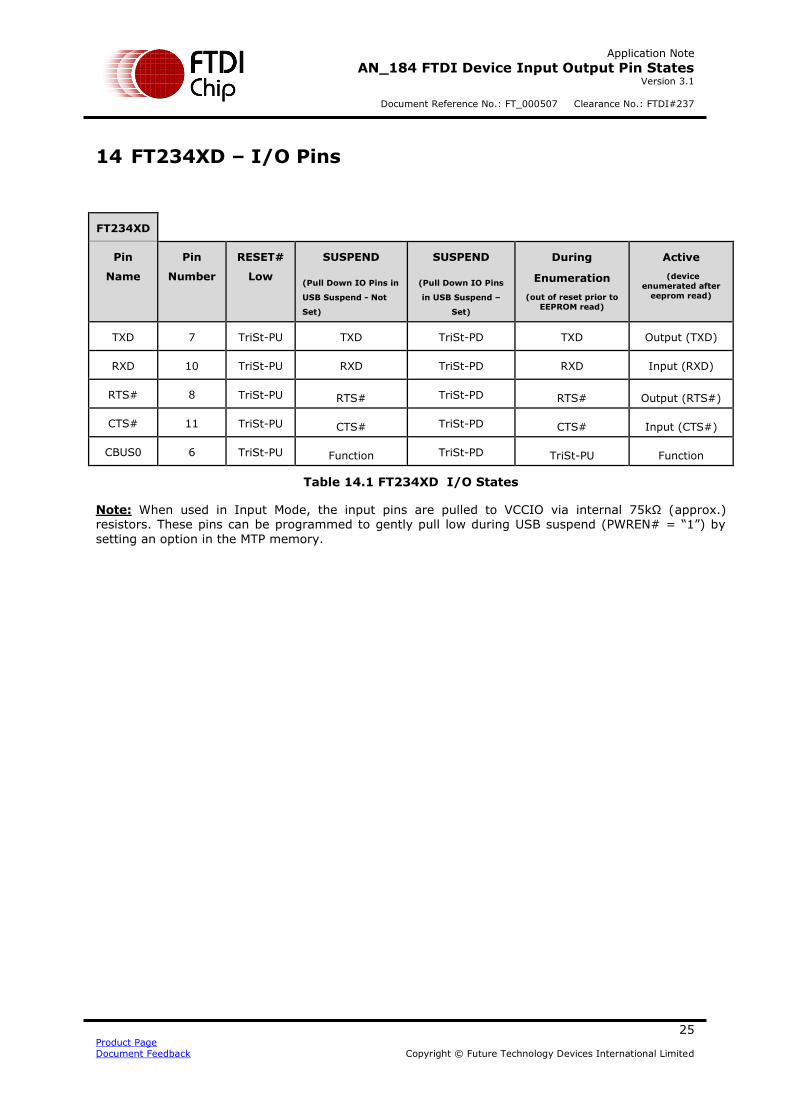
14 FT234XD – I/O Pins
FT234XD
Pin
Name
Pin
Number
RESET#
Low
SUSPEND
(Pull Down IO Pins in
USB Suspend - Not
Set)
SUSPEND
(Pull Down IO Pins
in USB Suspend –
Set)
During
Enumeration
(out of reset prior to
EEPROM read)
Active
(device
enumerated after
eeprom read)
TXD 7 TriSt-PU TXD TriSt-PD TXD Output (TXD)
RXD 10 TriSt-PU RXD TriSt-PD RXD Input (RXD)
RTS# 8 TriSt-PU RTS# TriSt-PD RTS# Output (RTS#)
CTS# 11 TriSt-PU CTS# TriSt-PD CTS# Input (CTS#)
CBUS0 6 TriSt-PU Function TriSt-PD TriSt-PU Function
Table 14.1 FT234XD I/O States
Note: When used in Input Mode, the input pins are pulled to VCCIO via internal 75kΩ (approx.) resistors. These pins can be programmed to gently pull low during USB suspend (PWREN# = “1”) by
setting an option in the MTP memory.
Page 27
Application Note
AN_184 FTDI Device Input Output Pin States Version 3.1
Document Reference No.: FT_000507 Clearance No.: FTDI#237
26 Product Page Document Feedback Copyright © Future Technology Devices International Limited
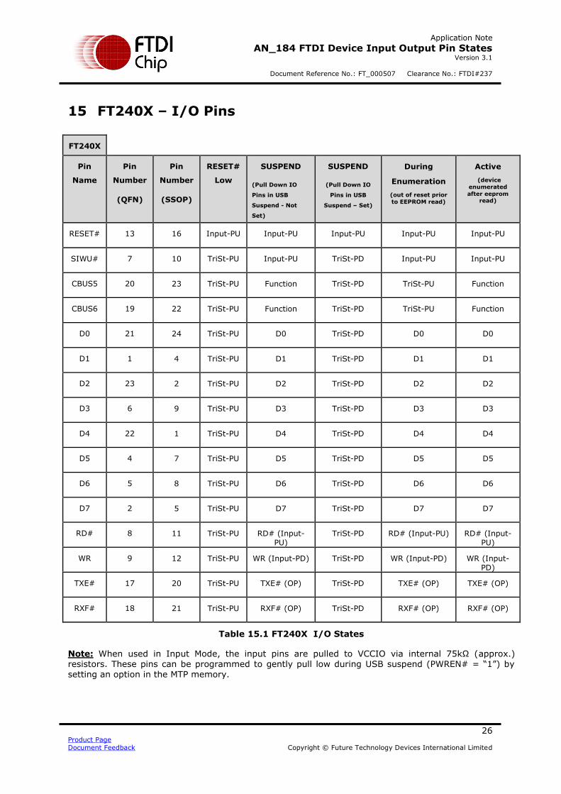
15 FT240X – I/O Pins
FT240X
Pin
Name
Pin
Number
(QFN)
Pin
Number
(SSOP)
RESET#
Low
SUSPEND
(Pull Down IO
Pins in USB
Suspend - Not
Set)
SUSPEND
(Pull Down IO
Pins in USB
Suspend – Set)
During
Enumeration
(out of reset prior
to EEPROM read)
Active
(device
enumerated
after eeprom read)
RESET# 13 16 Input-PU Input-PU Input-PU Input-PU Input-PU
SIWU# 7 10 TriSt-PU Input-PU TriSt-PD Input-PU Input-PU
CBUS5 20 23 TriSt-PU Function TriSt-PD TriSt-PU Function
CBUS6 19 22 TriSt-PU Function TriSt-PD TriSt-PU Function
D0 21 24 TriSt-PU D0 TriSt-PD D0 D0
D1 1 4 TriSt-PU D1 TriSt-PD D1 D1
D2 23 2 TriSt-PU D2 TriSt-PD D2 D2
D3 6 9 TriSt-PU D3 TriSt-PD D3 D3
D4 22 1 TriSt-PU D4 TriSt-PD D4 D4
D5 4 7 TriSt-PU D5 TriSt-PD D5 D5
D6 5 8 TriSt-PU D6 TriSt-PD D6 D6
D7 2 5 TriSt-PU D7 TriSt-PD D7 D7
RD# 8 11 TriSt-PU RD# (Input-PU)
TriSt-PD RD# (Input-PU) RD# (Input-PU)
WR 9 12 TriSt-PU WR (Input-PD) TriSt-PD WR (Input-PD) WR (Input-PD)
TXE# 17 20 TriSt-PU TXE# (OP) TriSt-PD TXE# (OP) TXE# (OP)
RXF# 18 21 TriSt-PU RXF# (OP) TriSt-PD RXF# (OP) RXF# (OP)
Table 15.1 FT240X I/O States
Note: When used in Input Mode, the input pins are pulled to VCCIO via internal 75kΩ (approx.) resistors. These pins can be programmed to gently pull low during USB suspend (PWREN# = “1”) by setting an option in the MTP memory.
Page 28
Application Note
AN_184 FTDI Device Input Output Pin States Version 3.1
Document Reference No.: FT_000507 Clearance No.: FTDI#237
27 Product Page Document Feedback Copyright © Future Technology Devices International Limited
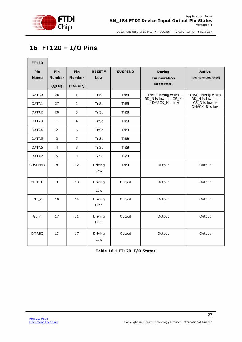
16 FT120 – I/O Pins
FT120
Pin
Name
Pin
Number
(QFN)
Pin
Number
(TSSOP)
RESET#
Low
SUSPEND
During
Enumeration
(out of reset)
Active
(device enumerated)
DATA0 26 1 TriSt TriSt TriSt, driving when RD_N is low and CS_N
or DMACK_N is low
TriSt, driving when RD_N is low and CS_N is low or
DMACK_N is low DATA1 27 2 TriSt TriSt
DATA2 28 3 TriSt TriSt
DATA3 1 4 TriSt TriSt
DATA4 2 6 TriSt TriSt
DATA5 3 7 TriSt TriSt
DATA6 4 8 TriSt TriSt
DATA7 5 9 TriSt TriSt
SUSPEND 8 12 Driving
Low
TriSt Output Output
CLKOUT 9 13 Driving
Low
Output Output Output
INT_n 10 14 Driving
High
Output Output Output
GL_n 17 21 Driving
High
Output Output Output
DMREQ 13 17 Driving
Low
Output Output Output
Table 16.1 FT120 I/O States
Page 29
Application Note
AN_184 FTDI Device Input Output Pin States Version 3.1
Document Reference No.: FT_000507 Clearance No.: FTDI#237
28 Product Page Document Feedback Copyright © Future Technology Devices International Limited
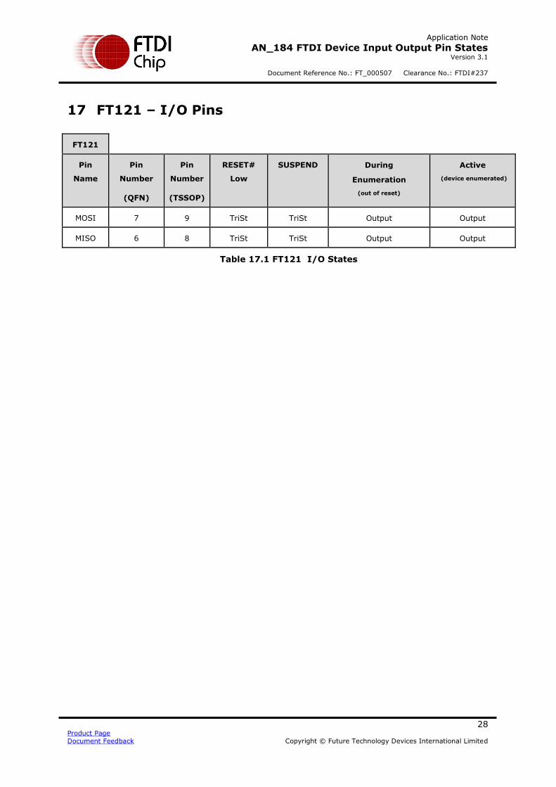
17 FT121 – I/O Pins
FT121
Pin
Name
Pin
Number
(QFN)
Pin
Number
(TSSOP)
RESET#
Low
SUSPEND
During
Enumeration
(out of reset)
Active
(device enumerated)
MOSI 7 9 TriSt TriSt Output Output
MISO 6 8 TriSt TriSt Output Output
Table 17.1 FT121 I/O States
Page 30
Application Note
AN_184 FTDI Device Input Output Pin States Version 3.1
Document Reference No.: FT_000507 Clearance No.: FTDI#237
29 Product Page Document Feedback Copyright © Future Technology Devices International Limited
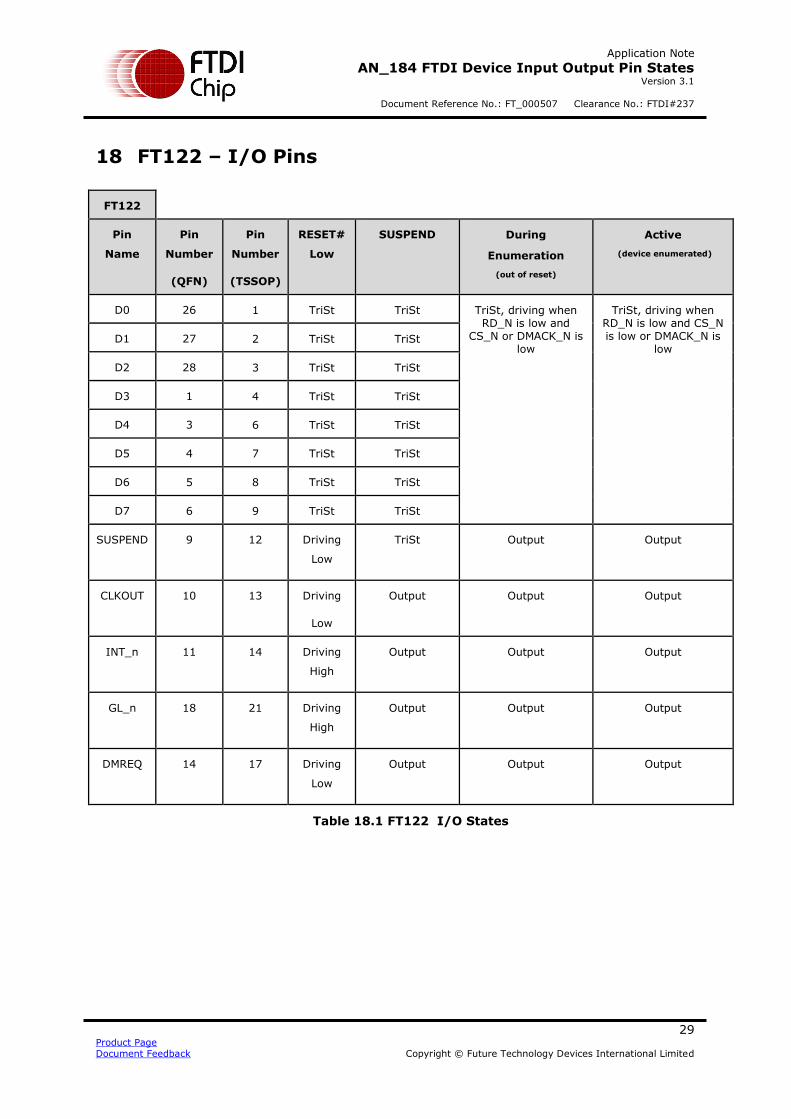
18 FT122 – I/O Pins
FT122
Pin
Name
Pin
Number
(QFN)
Pin
Number
(TSSOP)
RESET#
Low
SUSPEND
During
Enumeration
(out of reset)
Active
(device enumerated)
D0 26 1 TriSt TriSt TriSt, driving when RD_N is low and
CS_N or DMACK_N is low
TriSt, driving when RD_N is low and CS_N is low or DMACK_N is
low D1 27 2 TriSt TriSt
D2 28 3 TriSt TriSt
D3 1 4 TriSt TriSt
D4 3 6 TriSt TriSt
D5 4 7 TriSt TriSt
D6 5 8 TriSt TriSt
D7 6 9 TriSt TriSt
SUSPEND 9 12 Driving
Low
TriSt Output Output
CLKOUT 10 13 Driving
Low
Output Output Output
INT_n 11 14 Driving
High
Output Output Output
GL_n 18 21 Driving
High
Output Output Output
DMREQ 14 17 Driving
Low
Output Output Output
Table 18.1 FT122 I/O States
Page 31
Application Note
AN_184 FTDI Device Input Output Pin States Version 3.1
Document Reference No.: FT_000507 Clearance No.: FTDI#237
30 Product Page Document Feedback Copyright © Future Technology Devices International Limited
19 FT313H – I/O Pins
FT313
Pin Name Pin
Number
(QFN)
Pin
Number
(LQFP)
Pin
Number
(TQFP)
RESET# Low Active
AD0 2 2 2 TriSt Input/Output
AD1 3 3 3 TriSt Input/Output
AD2 4 4 4 TriSt Input/Output
AD3 5 5 5 TriSt Input/Output
AD4 7 7 7 TriSt Input/Output
AD5 8 8 8 TriSt Input/Output
AD6 9 9 9 TriSt Input/Output
AD7 10 10 10 TriSt Input/Output
AD8 11 11 11 TriSt Input/Output
AD9 12 12 12 TriSt Input/Output
AD10 13 13 13 TriSt Input/Output
AD11 14 14 14 TriSt Input/Output
AD12 16 16 16 TriSt Input/Output
AD13 17 17 17 TriSt Input/Output
AD14 18 18 18 TriSt Input/Output
AD15 19 19 19 TriSt Input/Output
Table 19.1 FT313H I/O States
Page 32
Application Note
AN_184 FTDI Device Input Output Pin States Version 3.1
Document Reference No.: FT_000507 Clearance No.: FTDI#237
31 Product Page Document Feedback Copyright © Future Technology Devices International Limited
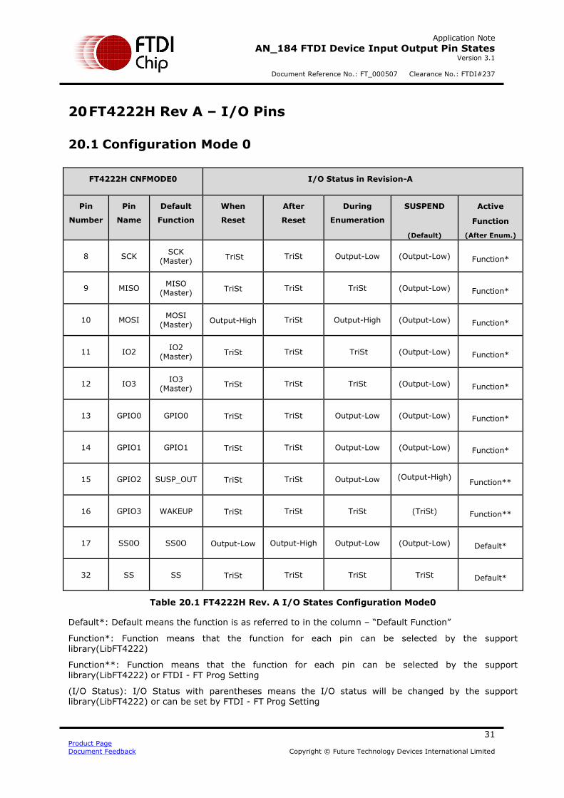
20 FT4222H Rev A – I/O Pins
20.1 Configuration Mode 0
FT4222H CNFMODE0 I/O Status in Revision-A
Pin
Number
Pin
Name
Default
Function
When
Reset
After
Reset
During
Enumeration
SUSPEND
(Default)
Active
Function
(After Enum.)
8 SCK SCK
(Master) TriSt TriSt Output-Low (Output-Low) Function*
9 MISO MISO
(Master) TriSt TriSt TriSt (Output-Low) Function*
10 MOSI MOSI
(Master) Output-High TriSt Output-High (Output-Low) Function*
11 IO2 IO2
(Master) TriSt TriSt TriSt (Output-Low) Function*
12 IO3 IO3
(Master) TriSt TriSt TriSt (Output-Low) Function*
13 GPIO0 GPIO0 TriSt TriSt Output-Low (Output-Low) Function*
14 GPIO1 GPIO1 TriSt TriSt Output-Low (Output-Low) Function*
15 GPIO2 SUSP_OUT TriSt TriSt Output-Low (Output-High) Function**
16 GPIO3 WAKEUP TriSt TriSt TriSt (TriSt) Function**
17 SS0O SS0O Output-Low Output-High Output-Low (Output-Low) Default*
32 SS SS TriSt TriSt TriSt TriSt Default*
Table 20.1 FT4222H Rev. A I/O States Configuration Mode0
Default*: Default means the function is as referred to in the column – “Default Function”
Function*: Function means that the function for each pin can be selected by the support library(LibFT4222)
Function**: Function means that the function for each pin can be selected by the support library(LibFT4222) or FTDI - FT Prog Setting
(I/O Status): I/O Status with parentheses means the I/O status will be changed by the support library(LibFT4222) or can be set by FTDI - FT Prog Setting
Page 33
Application Note
AN_184 FTDI Device Input Output Pin States Version 3.1
Document Reference No.: FT_000507 Clearance No.: FTDI#237
32 Product Page Document Feedback Copyright © Future Technology Devices International Limited
20.2 Configuration Mode 1
FT4222H CNFMODE1 I/O Status in Revision-A
Pin
Number
Pin
Name
Default
Function
When
Reset
After
Reset
During
Enumeration
SUSPEND
(Default)
Active
Function
(After Enum.)
8 SCK SCK
(Master) TriSt TriSt Output-Low (Output-Low) Function*
9 MISO MISO
(Master) TriSt TriSt TriSt (Output-Low) Function*
10 MOSI MOSI
(Master) Output-High TriSt Output-High (Output-Low) Function*
11 IO2 IO2
(Master) TriSt TriSt TriSt (Output-Low) Function*
12 IO3 IO3
(Master) TriSt TriSt TriSt (Output-Low) Function*
13 GPIO0 SS1O
(Master) TriSt TriSt Output-Low (Output-Low) Default*
14 GPIO1 SS2O
(Master) TriSt TriSt Output-Low (Output-Low) Default*
15 GPIO2 SUSP_OUT TriSt TriSt Output-Low (Output-High) Function**
16 GPIO3 WAKEUP TriSt TriSt TriSt (TriSt) Function**
17 SS0O SS0O Output-Low Output-High Output-Low (Output-Low) Default*
32 SS SS TriSt TriSt TriSt TriSt Default*
Table 20.2 FT4222H Rev. A I/O States Configuration Mode1
Default*: Default means the function is as referred to in the column – “Default Function”
Function*: Function means that the function for each pin can be selected by the support library(LibFT4222)
Function**: Function means that the function for each pin can be selected by the support library(LibFT4222) or FTDI - FT Prog Setting
(I/O Status): I/O Status with parentheses means the I/O status will be changed by the support
library(LibFT4222) or can be set by FTDI - FT Prog Setting
Page 34
Application Note
AN_184 FTDI Device Input Output Pin States Version 3.1
Document Reference No.: FT_000507 Clearance No.: FTDI#237
33 Product Page Document Feedback Copyright © Future Technology Devices International Limited
20.3 Configuration Mode 2
FT4222H CNFMODE2 I/O Status in Revision-A
Pin
Number
Pin
Name
Default
Function
When
Reset
After
Reset
During
Enumeration
SUSPEND
(Default)
Active
Function
(After Enum.)
8 SCK SCK
(Master) TriSt TriSt Output-Low (Output-Low) Function*
9 MISO MISO
(Master) TriSt TriSt TriSt (Output-Low) Function*
10 MOSI MOSI
(Master) Output-High TriSt Output-High (Output-Low) Function*
11 IO2 IO2
(Master) TriSt TriSt TriSt (Output-Low) Function*
12 IO3 IO3
(Master) TriSt TriSt TriSt (Output-Low) Function*
13 GPIO0 SS1O
(Master) TriSt TriSt Output-Low (Output-Low)
Default*
14 GPIO1 SS2O
(Master) TriSt TriSt Output-Low (Output-Low)
Default*
15 GPIO2 SS3O
(Master) TriSt TriSt Output-Low (Output-Low) Default*
16 GPIO3 WAKEUP TriSt TriSt TriSt (TriSt) Function**
17 SS0O SS0O Output-Low Output-High Output-Low (Output-Low) Default*
32 SS SS TriSt TriSt TriSt TriSt Default*
Table 20.3 FT4222H Rev. A I/O States Configuration Mode2
Default*: Default means the function is as referred to in the column – “Default Function”
Function*: Function means that the function for each pin can be selected by the support library(LibFT4222)
Function**: Function means that the function for each pin can be selected by the support library(LibFT4222) or FTDI - FT Prog Setting
(I/O Status): I/O Status with parentheses means the I/O status will be changed by the support
library(LibFT4222) or can be set by FTDI - FT Prog Setting
Page 35
Application Note
AN_184 FTDI Device Input Output Pin States Version 3.1
Document Reference No.: FT_000507 Clearance No.: FTDI#237
34 Product Page Document Feedback Copyright © Future Technology Devices International Limited
20.4 Configuration Mode 3
FT4222H CNFMODE3 I/O Status in Revision-A
Pin
Number
Pin
Name
Default
Function
When
Reset
After
Reset
During
Enumeration
SUSPEND
(Default)
Active
Function
(After Enum.)
8 SCK SCK
(Master) TriSt TriSt Output-Low (Output-Low) Function*
9 MISO MISO
(Master) TriSt TriSt TriSt (Output-Low) Function*
10 MOSI MOSI
(Master) Output-High TriSt Output-High (Output-Low) Function*
11 IO2 IO2
(Master) TriSt TriSt TriSt (Output-Low) Function*
12 IO3 IO3
(Master) TriSt TriSt TriSt (Output-Low) Function*
13 GPIO0 GPIO0 TriSt TriSt Output-Low (Output-Low) Function*
14 GPIO1 GPIO1 TriSt TriSt Output-Low (Output-Low) Function*
15 GPIO2 SUSP_OUT TriSt TriSt Output-Low Output-High Default*
16 GPIO3 WAKEUP TriSt TriSt TriSt (TriSt) Default*
17 SS0O SS0O Output-Low Output-High Output-Low (Output-Low) Default*
32 SS SS TriSt TriSt TriSt TriSt Default*
Table 20.4 FT4222H Rev. A I/O States Configuration Mode3
Default*: Default means the function is as referred to in the column – “Default Function”
Function*: Function means that the function for each pin can be selected by the support library(LibFT4222)
Function**: Function means that the function for each pin can be selected by the support library(LibFT4222) or FTDI - FT Prog Setting
(I/O Status): I/O Status with parentheses means the I/O status will be changed by the support
library(LibFT4222) or can be set by FTDI - FT Prog Setting
Page 36
Application Note
AN_184 FTDI Device Input Output Pin States Version 3.1
Document Reference No.: FT_000507 Clearance No.: FTDI#237
35 Product Page Document Feedback Copyright © Future Technology Devices International Limited
21 FT4222H Rev B,C,D – I/O Pins
21.1 Configuration Mode 0
FT4222H CNFMODE0 I/O Status in Revision-B,C,D
Pin
Number
Pin
Name
Default
Function
When
Reset
After
Reset
During
Enumeration
SUSPEND
(Default)
Active
Function
(After Enum.)
8 SCK SCK
(Master) TriSt TriSt Output-Low (TriSt) Function*
9 MISO MISO
(Master) TriSt TriSt TriSt (TriSt) Function*
10 MOSI MOSI
(Master) Output-High TriSt Output-High (TriSt) Function*
11 IO2 IO2
(Master) TriSt TriSt TriSt (TriSt) Function*
12 IO3 IO3
(Master) TriSt TriSt TriSt (TriSt) Function*
13 GPIO0 GPIO0 TriSt TriSt TriSt (TriSt) Function*
14 GPIO1 GPIO1 TriSt TriSt TriSt (TriSt) Function*
15 GPIO2 SUSP_OUT TriSt TriSt (Output-Low) (Output-High) Function**
16 GPIO3 WAKEUP TriSt TriSt TriSt (TriSt) Function**
17 SS0O SS0O Output-Low Output-High Output-High (Output-High) Default*
32 SS SS TriSt TriSt TriSt TriSt Default*
Table 21.1 FT4222H Rev. B, C, D I/O States Configuration Mode0
Default*: Default means the function is as referred to in the column – “Default Function”
Function*: Function means that the function for each pin can be selected by the support library(LibFT4222)
Function**: Function means that the function for each pin can be selected by the support library(LibFT4222) or FTDI - FT Prog Setting
(I/O Status): I/O Status with parentheses means the I/O status will be changed by the support library(LibFT4222) or can be set by FTDI - FT Prog Setting
Page 37
Application Note
AN_184 FTDI Device Input Output Pin States Version 3.1
Document Reference No.: FT_000507 Clearance No.: FTDI#237
36 Product Page Document Feedback Copyright © Future Technology Devices International Limited
21.2 Configuration Mode 1
FT4222H CNFMODE1 I/O Status in Revision-B,C,D
Pin
Number
Pin
Name
Default
Function
When
Reset
After
Reset
During
Enumeration
SUSPEND
(Default)
Active
Function
(After Enum.)
8 SCK SCK
(Master) TriSt TriSt Output-Low (TriSt) Function*
9 MISO MISO
(Master) TriSt TriSt TriSt (TriSt) Function*
10 MOSI MOSI
(Master) Output-High TriSt Output-High (TriSt) Function*
11 IO2 IO2
(Master) TriSt TriSt TriSt (TriSt) Function*
12 IO3 IO3
(Master) TriSt TriSt TriSt (TriSt) Function*
13 GPIO0 SS1O TriSt TriSt Output-High (Output-High) Default*
14 GPIO1 SS2O TriSt TriSt Output-High (Output-High) Default*
15 GPIO2 SUSP_OUT TriSt TriSt (Output-Low) (Output-High) Function**
16 GPIO3 WAKEUP TriSt TriSt TriSt (TriSt) Function**
17 SS0O SS0O Output-Low Output-High Output-High (Output-High) Default*
32 SS SS TriSt TriSt TriSt TriSt Default*
Table 21.2 FT4222H Rev. B, C, D I/O States Configuration Mode1
Default*: Default means the function is as referred to in the column – “Default Function”
Function*: Function means that the function for each pin can be selected by the support library(LibFT4222)
Function**: Function means that the function for each pin can be selected by the support library(LibFT4222) or FTDI - FT Prog Setting
(I/O Status): I/O Status with parentheses means the I/O status will be changed by the support library(LibFT4222) or can be set by FTDI - FT Prog Setting
Page 38
Application Note
AN_184 FTDI Device Input Output Pin States Version 3.1
Document Reference No.: FT_000507 Clearance No.: FTDI#237
37 Product Page Document Feedback Copyright © Future Technology Devices International Limited
21.3 Configuration Mode 2
FT4222H CNFMODE2 I/O Status in Revision-B,C,D
Pin
Number
Pin
Name
Default
Function
When
Reset
After
Reset
During
Enumeration
SUSPEND
(Default)
Active
Function
(After Enum.)
8 SCK SCK
(Master) TriSt TriSt Output-Low (TriSt) Function*
9 MISO MISO
(Master) TriSt TriSt TriSt (TriSt) Function*
10 MOSI MOSI
(Master) Output-High TriSt Output-High (TriSt) Function*
11 IO2 IO2
(Master) TriSt TriSt TriSt (TriSt) Function*
12 IO3 IO3
(Master) TriSt TriSt TriSt (TriSt) Function*
13 GPIO0 SS1O TriSt TriSt Output-High (Output-High) Default*
14 GPIO1 SS2O TriSt TriSt Output-High (Output-High) Default*
15 GPIO2 SS3O TriSt TriSt Output-High (Output-High) Default*
16 GPIO3 WAKEUP TriSt TriSt TriSt (TriSt) Function**
17 SS0O SS0O Output-Low Output-High Output-High (Output-High) Default*
32 SS SS TriSt TriSt TriSt TriSt Default*
Table 21.3 FT4222H Rev. B, C, D I/O States Configuration Mode2
Default*: Default means the function is as referred to in the column – “Default Function”
Function*: Function means that the function for each pin can be selected by the support library(LibFT4222)
Function**: Function means that the function for each pin can be selected by the support library(LibFT4222) or FTDI - FT Prog Setting
(I/O Status): I/O Status with parentheses means the I/O status will be changed by the support
library(LibFT4222) or can be set by FTDI - FT Prog Setting
Page 39
Application Note
AN_184 FTDI Device Input Output Pin States Version 3.1
Document Reference No.: FT_000507 Clearance No.: FTDI#237
38 Product Page Document Feedback Copyright © Future Technology Devices International Limited
21.4 Configuration Mode 3
FT4222H CNFMODE3 I/O Status in Revision-B,C,D
Pin
Number
Pin
Name
Default
Function
When
Reset
After
Reset
During
Enumeration
SUSPEND
(Default)
Active
Function
(After Enum.)
8 SCK SCK
(Master) TriSt TriSt Output-Low (TriSt) Function*
9 MISO MISO
(Master) TriSt TriSt TriSt (TriSt) Function*
10 MOSI MOSI
(Master) Output-High TriSt Output-High (TriSt) Function*
11 IO2 IO2
(Master) TriSt TriSt TriSt (TriSt) Function*
12 IO3 IO3
(Master) TriSt TriSt TriSt (TriSt) Function*
13 GPIO0 GPIO0 TriSt TriSt TriSt (TriSt) Function*
14 GPIO1 GPIO1 TriSt TriSt TriSt (TriSt) Function*
15 GPIO2 SUSP_OUT TriSt TriSt (Output-Low) (Output-High) Default*
16 GPIO3 WAKEUP TriSt TriSt TriSt (TriSt) Default*
17 SS0O SS0O Output-Low Output-High Output-High (Output-High) Default*
32 SS SS TriSt TriSt (TriSt) TriSt Default*
Table 21.4 FT4222H Rev. B, C, D I/O States Configuration Mode3
Default*: Default means the function is as referred to in the column – “Default Function”
Function*: Function means that the function for each pin can be selected by the support library(LibFT4222)
Function**: Function means that the function for each pin can be selected by the support library(LibFT4222) or FTDI - FT Prog Setting
(I/O Status): I/O Status with parentheses means the I/O status will be changed by the support
library(LibFT4222) or can be set by FTDI - FT Prog Setting.
Page 40
Application Note
AN_184 FTDI Device Input Output Pin States Version 3.1
Document Reference No.: FT_000507 Clearance No.: FTDI#237
39 Product Page Document Feedback Copyright © Future Technology Devices International Limited
22 Contact Information
Head Office – Glasgow, UK Future Technology Devices International Limited Unit 1, 2 Seaward Place, Centurion Business Park Glasgow G41 1HH United Kingdom Tel: +44 (0) 141 429 2777 Fax: +44 (0) 141 429 2758 E-mail (Sales) [email protected] E-mail (Support) [email protected] E-mail (General Enquiries) [email protected]
Branch Office – Taipei, Taiwan Future Technology Devices International Limited (Taiwan) 2F, No. 516, Sec. 1, NeiHu Road
Taipei 114 Taiwan , R.O.C. Tel: +886 (0) 2 8797 1330 Fax: +886 (0) 2 8751 9737 E-mail (Sales) [email protected] E-mail (Support) [email protected] E-mail (General Enquiries) [email protected]
Branch Office – Tigard, Oregon, USA Future Technology Devices International Limited (USA) 7130 SW Fir Loop Tigard, OR 97223-8160 USA Tel: +1 (503) 547 0988 Fax: +1 (503) 547 0987 E-Mail (Sales) [email protected] E-Mail (Support) [email protected] E-Mail (General Enquiries) [email protected]
Branch Office – Shanghai, China Future Technology Devices International Limited (China) Room 1103, No.666 West Huaihai Road,
Shanghai, 200052 China Tel: +86 21 62351596 Fax: +86 21 62351595 E-mail (Sales) [email protected] E-mail (Support) [email protected] E-mail (General Enquiries) [email protected]
Web Site http://ftdichip.com
Distributor and Sales Representatives
Please visit the Sales Network page of the FTDI Web site for the contact details of our distributor(s) and sales representative(s) in your country.
System and equipment manufacturers and designers are responsible to ensure that their systems, and any Future Technology
Devices International Ltd (FTDI) devices incorporated in their systems, meet all applicable safety, regulatory and system-level
performance requirements. All application-related information in this document (including application descriptions, suggested
FTDI devices and other materials) is provided for reference only. While FTDI has taken care to assure it is accurate, this information is subject to customer confirmation, and FTDI disclaims all liability for system designs and for any applications
assistance provided by FTDI. Use of FTDI devices in life support and/or safety applications is entirely at the user’s risk, and the
user agrees to defend, indemnify and hold harmless FTDI from any and all damages, claims, suits or expense resulting from
such use. This document is subject to change without notice. No freedom to use patents or other intellectual property rights is
implied by the publication of this document. Neither the whole nor any part of the information contained in, or the product
described in this document, may be adapted or reproduced in any material or electronic form without the prior written consent
of the copyright holder. Future Technology Devices International Ltd, Unit 1, 2 Seaward Place, Centurion Business Park,
Glasgow G41 1HH, United Kingdom. Scotland Registered Company Number: SC136640
Page 41
Application Note
AN_184 FTDI Device Input Output Pin States Version 3.1
Document Reference No.: FT_000507 Clearance No.: FTDI#237
40 Product Page Document Feedback Copyright © Future Technology Devices International Limited
Appendix A – References
Document References
FT232R USB UART IC Data Sheet
FT245R USB FIFO Data Sheet
FT232H Single Channel Hi-Speed USB to Multipurpose UART/FIFO IC Data Sheet
FT2232H Hi-Speed Dual USB UART/FIFO IC Data Sheet
FT4232H Hi-Speed Quad USB UART IC Data Sheet
FT2232D Dual USB UART/FIFO IC Data Sheet
FT200XD Full-Speed USB to I2C bridge in 10 pin DFN package Data Sheet
FT201X Full-Speed USB to I2C bridge Data Sheet
FT220X Full-Speed USB to 4-bit SPI/FT1248 bridge Data Sheet
FT221X Full-Speed USB to 8-bit SPI/FT1248 bridge Data Sheet
FT230X Full-Speed USB to basic UART Data Sheet
FT231X Full-Speed USB to full handshake UART Data Sheet
FT234XD Full-Speed USB to basic UART Data Sheet
FT240X Full-Speed USB to 8-bit FIFO Data Sheet
FT120 USB Full-Speed Device Controller Data Sheet
FT121 USB Full-Speed Device Controller Data Sheet
FT122 USB Full-Speed Device Controller Data Sheet
FT313H Hi-Speed Host Controller
FT4222H Hi-Speed Quad SPI/I2C IC Data Sheet
Acronyms and Abbreviations
Terms Description
PD Internal pull-down resistor to GND
PU Internal pull-up resistor to VCCIO
TriSt High-impedance off-state (‘tristate’)
USB Universal Serial Bus
USB-IF USB Implementers Forum
Page 42
Application Note
AN_184 FTDI Device Input Output Pin States Version 3.1
Document Reference No.: FT_000507 Clearance No.: FTDI#237
41 Product Page Document Feedback Copyright © Future Technology Devices International Limited
Appendix B – List of Tables & Figures
List of Tables
Table 2.1 FT232R I/O States ............................................................................................... 4
Table 2.2 FT232R CBUS Selected Functions ........................................................................... 5
Table 3.1 FT245R I/O States ............................................................................................... 6
Table 4.1 FT232H I/O States ............................................................................................... 7
Table 4.2 FT232H Selected Functions ................................................................................... 8
Table 5.1 FT2232H I/O States Channel A .............................................................................. 9
Table 5.2 FT2232H I/O States Channel B ............................................................................ 10
Table 5.3 FT2232H Selected Functions ................................................................................ 11
Table 6.1 FT4232H I/O States Channel A ............................................................................ 12
Table 6.2 FT4232H I/O States Channel B ............................................................................ 12
Table 6.3 FT4232H I/O States Channel C ............................................................................ 13
Table 6.4 FT4232H I/O States Channel D ............................................................................ 13
Table 6.5 Selected Functions ............................................................................................. 14
Table 7.1 FT2232D I/O States Channel A ............................................................................ 15
Table 7.2 FT2232D I/O States Channel B ............................................................................ 16
Table 7.3 Pin Definition by Chip Mode - Channel A ............................................................... 17
Table 7.4 Pin Definition by Chip Mode - Channel B ............................................................... 18
Table 8.1 FT200XD I/O States ............................................................................................ 19
Table 9.1 FT201X I/O States ............................................................................................. 20
Table 10.1 FT220X I/O States ............................................................................................ 21
Table 11.1 FT221X I/O States ............................................................................................ 22
Table 12.1 FT230X I/O States ............................................................................................ 23
Table 13.1 FT231X I/O States ............................................................................................ 24
Table 14.1 FT234XD I/O States ......................................................................................... 25
Table 15.1 FT240X I/O States ............................................................................................ 26
Table 16.1 FT120 I/O States ............................................................................................. 27
Table 17.1 FT121 I/O States ............................................................................................. 28
Table 18.1 FT122 I/O States ............................................................................................. 29
Table 19.1 FT313H I/O States ........................................................................................... 30
Table 20.1 FT4222H Rev. A I/O States Configuration Mode0 ................................................... 31
Table 20.2 FT4222H Rev. A I/O States Configuration Mode1 ................................................... 32
Table 20.3 FT4222H Rev. A I/O States Configuration Mode2 ................................................... 33
Table 20.4 FT4222H Rev. A I/O States Configuration Mode3 ................................................... 34
Table 21.1 FT4222H Rev. B, C, D I/O States Configuration Mode0 ........................................... 35
Table 21.2 FT4222H Rev. B, C, D I/O States Configuration Mode1 ........................................... 36
Page 43
Application Note
AN_184 FTDI Device Input Output Pin States Version 3.1
Document Reference No.: FT_000507 Clearance No.: FTDI#237
42 Product Page Document Feedback Copyright © Future Technology Devices International Limited
Table 21.3 FT4222H Rev. B, C, D I/O States Configuration Mode2 ........................................... 37
Table 21.4 FT4222H Rev. B, C, D I/O States Configuration Mode3 ........................................... 38
List of Figures
NA
Page 44
Application Note
AN_184 FTDI Device Input Output Pin States Version 3.1
Document Reference No.: FT_000507 Clearance No.: FTDI#237
43 Product Page Document Feedback Copyright © Future Technology Devices International Limited
Appendix C – Revision History
Document Title: AN_184 FTDI Device Input Output Pin States
Document Reference No.: FT_000507
Clearance No.: FTDI#237
Product Page: http://www.ftdichip.com/FTProducts.htm
Document Feedback: Send Feedback
Revision Changes Date
1.0 Initial Release 2011-11-24
2.0 Updated to include FT-X series, FT12 series & FT313H 2012-03-13
3.0 Updated to include FT4222H 2015-09-10
3.1
Updated FT4222H rev. D I/O Pins in section 21.
Updated Table 2.2 Bit bang WR# strobe CBUS availability.
2018-04-19