Page 1
FUNCTIONAL NANOPLASMONIC
DEVICES AND NOVEL PHOTONIC
MATERIALS
A THESIS SUBMITTED TO
THE GRADUATE SCHOOL OF ENGINEERING AND SCIENCE
OF BILKENT UNIVERSITY
IN PARTIAL FULFILLMENT OF THE REQUIREMENTS FOR
THE DEGREE OF
MASTER OF SCIENCE
IN
ELECTRICAL AND ELECTRONICS ENGINEERING
By
Enes Battal
June, 2015
Page 2
ii
FUNCTIONAL NANOPLASMONIC DEVICES AND NOVEL PHOTONIC
MATERIALS
By Enes Battal
June, 2015
We certify that we have read this thesis and that in our opinion it is fully
adequate, in scope and in quality, as a thesis for the degree of Master of Science.
_______________________________
Assist. Prof. Dr. Ali Kemal Okyay (Advisor)
_______________________________
Assoc. Prof. Dr. Vakur Behçet Ertürk
_______________________________
Assoc. Prof. Dr. Hamza Kurt
Approved for the Graduate School of Engineering and Science:
_________________________
Prof. Dr. Levent Onural
Director of the Graduate School
Page 3
iii
ABSTRACT
FUNCTIONAL NANOPLASMONIC DEVICES AND
NOVEL PHOTONIC MATERIALS
Enes Battal
M.S. in Electrical and Electronics Engineering
Advisor: Assist. Prof. Dr. Ali Kemal Okyay
June, 2015
Plasmonics is one of the pillars of nanophotonics involving light matter
interactions. Its applications found very wide range covering photovoltaics, photo-
detection, optical communication, surface enhanced infrared absorption and Raman
spectroscopy, infrared and THz imaging. Although the number of applications is very
high, the underlying plasmonic structures are limited. In this thesis, we utilize a
common plasmonic resonator structure namely metal-insulator-metal (MIM resonators)
to realize active beam steering in the infrared spectrum. We investigate radiation
characteristics of a phased array antenna formed by MIM resonators.
Materials-wise, low intrinsic loss, CMOS compatibility and bio-compatibility
are among the crucial requirements for various applications of plasmonics. Noble
metals are the dominant materials used in plasmonics to get high localization of the
incident field among which gold and silver face serious challenges due to high intrinsic
loss and lack of CMOS compatibility. We introduce InN as a novel plasmonic material
thanks to its high concentration of free carriers and investigate its optical characteristics
in the IR spectrum. We form a proof-of-concept absorber and investigate its plasmon
excitation characteristics. On the other hand, we introduce another material ZnO, non-
plasmonic, suitable for infrared imaging purposes with strong absorption characteristics.
Optical modulators are at the very heart of active light manipulation
technologies such as integrated optics, bio-sensing, telecommunications, radio
frequency and terahertz applications. Although various modulation schemes
Page 4
iv
have been realized, the underlying mechanisms providing modulation did not
change significantly. The common modulation methods can be listed as free
carrier dispersion, thermo-optic method, use of liquid crystals, magneto-optical,
optically nonlinear materials and recently introduced solid-state phase-change
materials. Here we introduce another mechanism called resistive switching for
optical modulation in the infrared spectrum. We investigate electrical resistive
switching characteristics of an Al/ZnO/Si stack and optical modulation
characteristics under electrical bias. We obtain hysteretic modulation in the
reflection spectrum. We also investigate the thermo-optic modulation
characteristics of atomic layer deposited ZnO through spectroscopic
ellipsometry and realization of actively reconfigurable reflector surface.
Keywords: Electro-optic, thermo-optic, infrared, plasmonics.
Page 5
v
ÖZET
İŞLEVSEL NANOPLAZMONİK AYGITLAR VE YENİ
FOTONİK MALZEMELER
Enes Battal
Elektrik ve Elektronik Mühendisliği, Yüksek Lisans
Tez Danışmanı: Yrd. Doç Dr. Ali Kemal Okyay
Haziran, 2015
Plasmonik ışık ve madde arasındaki etkiletişimi inceleyen etkin nanofotonik
alanlarından birisidir. Uygulama olarak güneş enerjısı, ışık detektörleri, optik iletişim,
yüzey geliştirilmiş kızılötesi and Raman spektroskopi, kızılötesi and terahertz
görüntüleme gibi alanları kapsamaktadır. Uygulama alanları çok olmasına ragmen
plazmonik etkilerin gözlemlendiği yapılar limitlidir. Bu tezde, bilinen bir plazmonik
yapı olan metal-yalıtkan-metal rezonatörlerin kızılötesi spektrumda aktif ışık
yönlendirme uygulaması incelenecektir. Bu rezonatörlerle oluşturulan faz dizi anten
konfigurasyonunun yayılma karakteristikleri incelenecektir.
Malzeme özellikleri açısından plazmonik uygulamalarda düşük iç kayıp
CMOS fabrikasyon uyumluluğu ve biyo-uygunluk aranan kritik özellikler arasında
gelmektedir. Plazmon uyarma malzemesi olarak asil metaller yüksek ışık lokalizasyonu
için çok yaygın olarak kullanılmaktadır. Bunların arasından altın ve gümüş yüksek iç
kayıp ve CMOS fabrikasyon uyumsuzluğu sorunlarını göstermektedir. Bu çalışmada
yüksek sayıdaki serbest yük taşımasındasından olayı indiyum-nitratı CMOS
fabrikasyonuna uygun kızılötesi plazmonik malzeme olarak incelenmektedir. Indiyum
nitratın kızılötesi optik özellikleri, kızılötesi soğurucu uygulaması ve plazmon
karakteristikleri incelenecektir. Diğer yandan, çinko-oksit alternatif plazmonik olmayan
kızılötesi görüntüleme çalışmalarına uygun yüksek soğurucu özellikler gösteren
malzeme olarak incelenecektir.
Page 6
vi
Optik modülatörler entegre optik, biyo-algılama, telekomunikasyon,
radio frekansı ve terahertz uygulamaları gibi aktif ışık manipülasyon
teknolojilerinin kalbinde bulunmaktadır. Bu uygulamalar için birden fazla optik
modülasyon şemaları gerçekleştirilmiş olmasına ragmen altta yatan optik
modülasyon mekanizmeleri çok değişmemiştir. En sık kullanılan modülasyon
mekanizmaları arasında serbest yük kontrolü, termo-optik yöntem, sıvı kristal,
opto-manyetik, lineer olmayan ve yeni ortaya çıkan katı katman faz değişimi
malzemeleri yer almaktadır. Burada, direnç değişimi yöntemi yeni bir kızılötesi
aktif modülasyon tekniği olarak sunulmaktadır. Al/ZnO/Si yığınının elektriksel
direnç değişimi karakteristikleri ve elektrik uygulanması sırasında optik
modülasyon karakteristikleri incelenmektedir. Işısal yansıma spektrumunda aktif
histeresiz gösteren modülasyon gözlemlenmektedir. Bu çalışmanın yanı sıra,
atomik katman kaplama tekniği ile büyütülmüş çinko-oksit malzemenin termo-
optik modülasyön karakteristikleri de incelenmiştir. Bu malzeme spektroskopik
elipsometre ile incelenmiş ve bununla aktif olarak değiştirilebilen yansıma
yüzeyi tasarlanmıştır.
Anahtar Sözcükler: Elektro-optik, termo-optik, kızılötesi, plazmonik.
Page 7
vii
Acknowledgement
I am deeply grateful to Prof. Ali Kemal Okyay for his guidance and patience
throughout my master’s degree. He was my research advisor in not only my
graduate years but also undergraduate years. He was an excellent supervisor and
I am happy to be a member of his research team. I have learned a lot from him
and always be grateful for everything he has done for me.
I would like to thank Prof. Vakur Ertürk and Prof. Hamza Kurt for being
members of my thesis committee and making this thesis better with their
valuable opinion.
I acknowledge TUBITAK (The Scientific and Technological Research Council
of Turkey) for providing me a M.Sc. scholarship and funding research through
TUBITAK-BIDEB. This work was supported by TUBITAK with grant numbers
109E044, 112M004, 112E052, 112M482, and 113M815.
I would like to thank our group members Fatih Bilge Atar, Feyza Bozkurt Oruç,
Furkan Çimen, Yunus Emre Kesim, Ali Cahit Köşger Berk Berkan Turgut, Sami
Bolat, Burak Tekcan, Ayse Özcan, Elif Özgöztaşı, Amin Nazirzadeh, Levent
Aygün, Amir Ghobadi, Abdullah Gök, Seyma Canik, Gamze Ulusoy,
Muhammed Maiz Ghauri Mehrab Ramzan and Sabri Alkış for making my
graduate studies journey enjoyable.
Finally, my deepest gratitude goes to my family who have their signature at any
success that I have achieved and will ever achieve throughout my entire life
thanks to their endless love and support. I am extremely pleased to dedicate this
thesis to my family.
Page 8
viii
Contents
Chapter 1 – Introduction .................................................................................... 1
1.1. Plasmonics .......................................................................................... 1
1.2. Optical modulation schemes .............................................................. 2
1.3. Thesis Overview ................................................................................. 3
Chapter 2 – Methods ........................................................................................... 5
2.1. Finite difference time domain (FDTD) method ................................. 5
2.2. Spectroscopic ellipsometry ................................................................. 6
Chapter 3 – Metal insulator metal plasmonic infrared beam steering .......... 9
3.1 Introduction ......................................................................................... 9
3.2. Device structure and simulation setup .......................................................... 10
3.3 Results and discussion ..................................................................................... 11
3.3.1 Radiation characteristics of a single resonator ............................................ 11
3.3.2 Phased array antenna characteristics ........................................................... 13
3.4. Conclusion ...................................................................................................... 16
Chapter 4 – InN based infrared plasmonics .................................................. .17
4.1. Introduction ...................................................................................... 17
4.2. Sample preparation ......................................................................................... 18
4.3. Optical characterization .................................................................................. 19
4.4. Device analysis ............................................................................................... 21
4.5. Conclusion ...................................................................................................... 25
Chapter 5 – Optical characterization of atomic layer deposited ZnO as a
novel bolometric material ............................................................ 26
5.1. Introduction ...................................................................................... 26
5.2. Optical Properties ............................................................................. 27
Page 9
ix
5.3. Device Analysis ................................................................................ 32
5.4. Conclusion ........................................................................................ 33
Chapter 6 – ZnO as an alternative thermo-optic material ............................ 35
6.1 Introduction ....................................................................................... 35
6.2. Ellipsometric Characterization ......................................................... 36
6.3. Actively Tunable Surface .............................................................................. 41
6.4. Conclusion ....................................................................................................... 43
Chapter 7 – Electro-optic modulation using a novel mechanism: resistive
switching ...................................................................................... 44
7.1. Introduction ...................................................................................... 44
7.2. Device structure ................................................................................ 45
7.3. Electrical characterization ................................................................ 46
7.4. Optoelectronic characterization ........................................................ 48
7.5. Conclusion ....................................................................................... .51
Conclusion .......................................................................................................................... 52
Bibliography ....................................................................................................... 54
Page 10
x
List of Figures
Figure 2.1 – An exemplary simulation environment ............................................ 6
Figure 2.2 – Depiction of a rotation compensator-analyzer spectroscopic
ellipsometers device .............................................................................................. 7
Figure 3.1 – The phased array antenna like configuration of MIM resonators having
different width values. Copyright 2013 Optical Society of America .................................... .11
Figure 3.2 – (a) MIM resonator unit having right (R-SP) and left (L-SP) propagating
SPs. b) A standing wave is formed within the MIM cavity due to Fabry-Perot
resonance. c) Radiation pattern of an MIM resonator unit resembling similarity to that
of a dipole except with the asymmetry in the front and back intensities. Copyright 2013
Optical Society of America ..................................................................................................... 12
Figure 3.3 – (a) The front lobe of the phased array-like MIM structure shifts by 8.75o
and the back lobe shifts by 2.35o when nSi changes by 0.15. b) Normalized radiation
intensity (|E|2n) at the center of the front lobe shifts continuously and its amplitude
increases by decreasing nSi . Copyright 2013 Optical Society of America ............................ 14
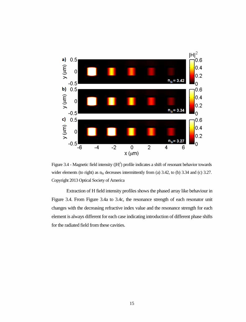
Figure 3.4 – Magnetic field intensity (|H|2) profile indicates a shift of resonant behavior
towards wider elements (to right) as nSi decreases intermittently from (a) 3.42, to (b)
3.34 and (c) 3.27. Copyright 2013 Optical Society of America ............................................. 15
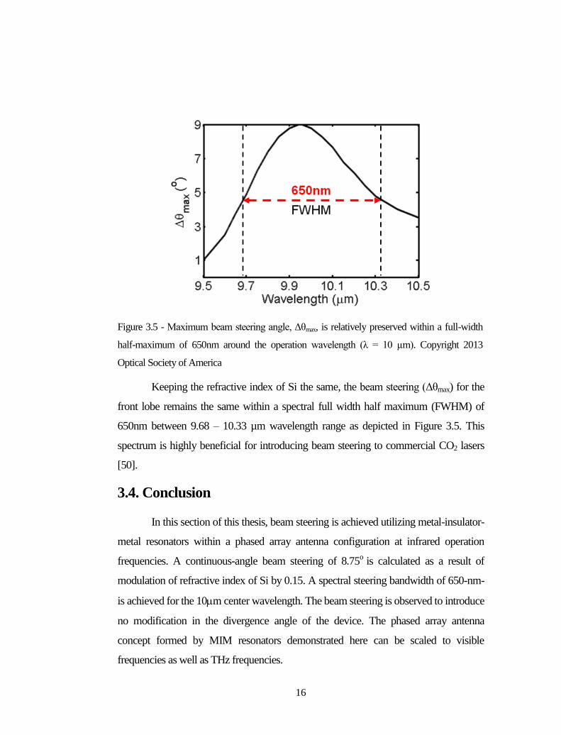
Figure 3.5 – Maximum beam steering angle, Δθmax, is relatively preserved within a
full-width half-maximum of 650nm around the operation wavelength (λ = 10 µm).
Copyright 2013 Optical Society of America............................................................................ 16
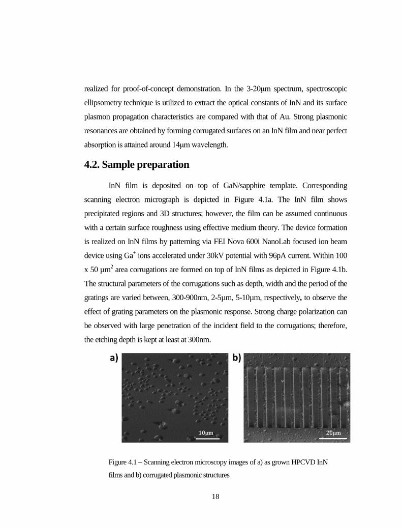
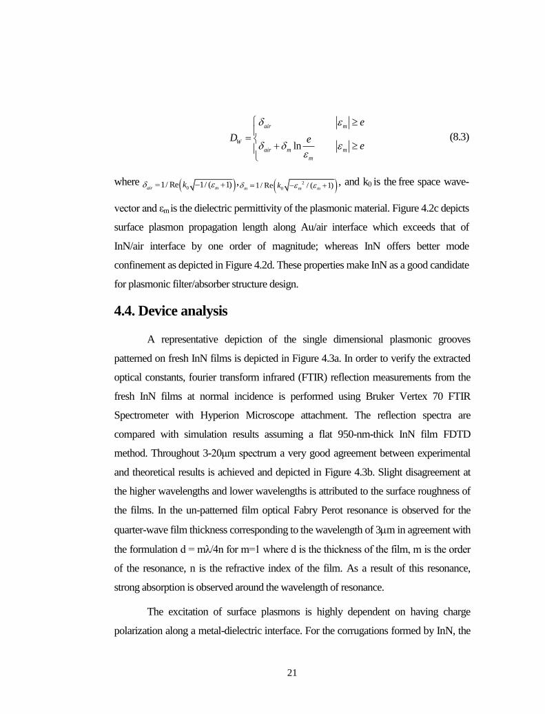
Figure 4.1 – Scanning electron microscopy images of a) as grown HPCVD InN films
and b) corrugated plasmonic structures ............................................................................. 18
Page 11
xi
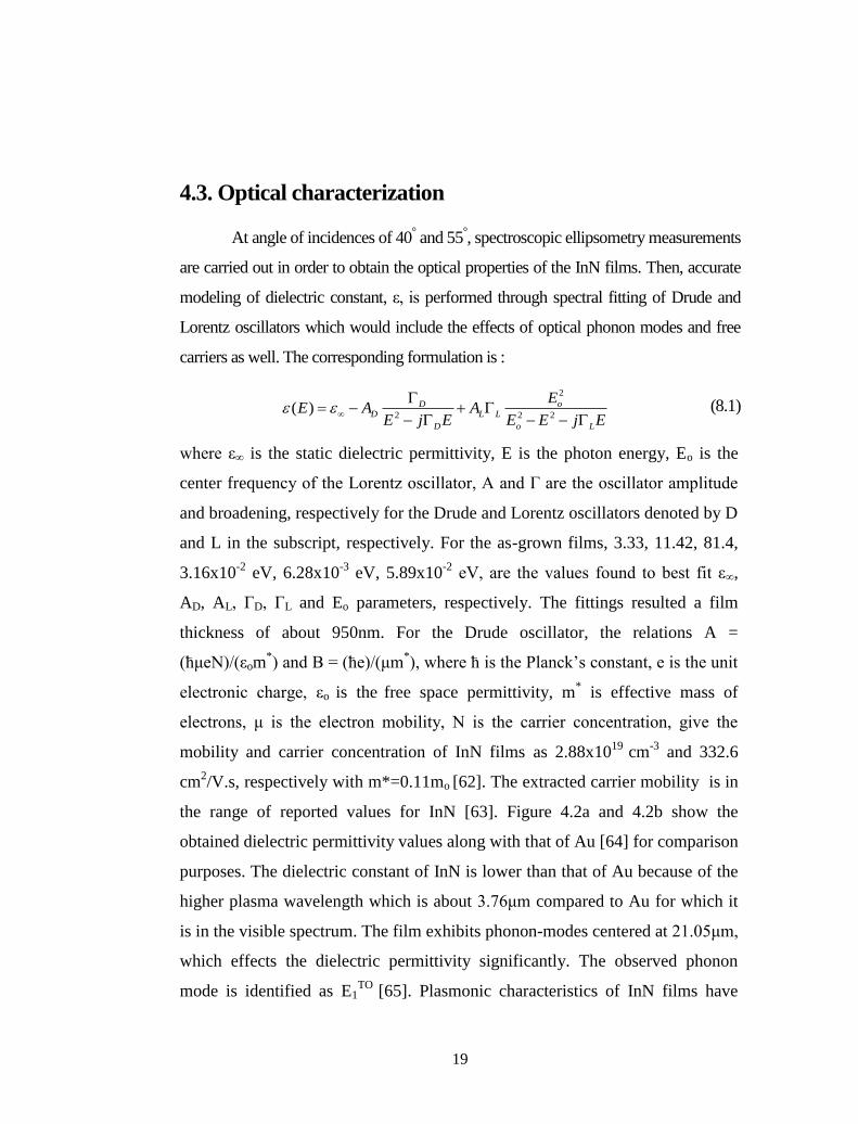
Figure 4.2 – Comparison of optical properties of Au and InN for a) real and b)
imaginary parts of their dielectric permittivity, c) plasmon propagation length
and d) mode size assuming they contact with air interface. ................................ 20
Figure 4.3 – Device structure with reflection characteristics. a) Representative image
for fresh and corrugated films. b) FTIR reflection spectra of the un-patterned film
agrees well with FDTD simulations c) The patterned grating structure with the period
(P) of 10μm and width (W) of 6μm shows surface plasmon assisted strong absorption
at around 14μm. d) The structure exhibits plasmon resonance in TM polarization and
no- plasmonic resonance at TE polarization as expected. ................................................ 22
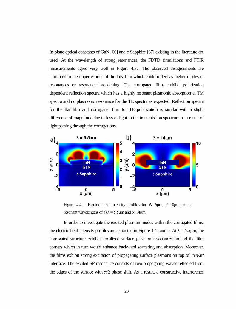
Figure 4.4 – Electric field intensity profiles for W=6μm, P=10μm, at the resonant
wavelengths of a) λ = 5.5μm and b) 14μm ........................................................................ 23
Figure 4.5 – Reflection spectra for different structure parameters under TM polarized
light indicate that the resonant wavelengths of the plasmon modes red-shift with the
increasing structure parameters. ......................................................................................... 24
Figure 5.1 – ALD deposited ZnO optical constants for various deposition
temperatures. (a) Real (') and (b) Imaginary ('') parts of the dielectric constants
of the ALD grown ZnO films as a function of deposition temperature. Metallic
behavior is dominant at higher temperatures due to increased concentration of
free carriers. Copyright 2014 John Wiley and Sons ................................................. 30
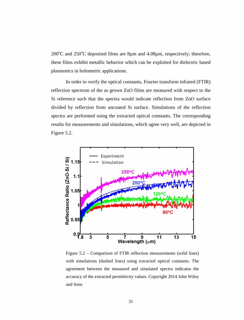
Figure 5.2 – Comparison of FTIR reflection measurements with simulations
using extracted optical constants. Copyright 2014 John Wiley and Sons ................ 31
Figure 5.3 – Reference structures depiction with absorption characteristics for
different materials. (a) 3D depiction of reference structure. (b) FDTD simulation
of average absorption for both ZnO and Si3N4 films in 8-12µm spectrum. (c)
The spectral absorption for all of the compared films. Copyright 2014 John Wiley
and Sons ................................................................................................................ 33
Page 12
xii
Figure 6.1 – Near visible optical constants of the ZnO film. a) Thermal
dependence of the real part of the refractive index in 300-1600nm spectrum.
The inset shows the sub-bandgap region. b) Variation in the refractive index for
temperature increase from 23oC to 200
oC. c) Thermal dependence of extinction
spectra showing red-shift of the band-edge due to thermal expansion ............... 39
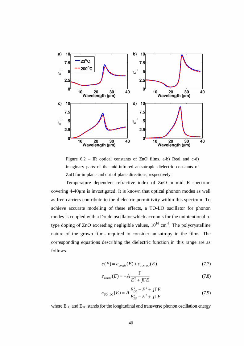
Figure 6.2 – IR optical constants of ZnO films. a-b) Real and c-d) imaginary
parts of the mid-infrared anisotropic dielectric constants of ZnO for in-plane and
out-of-plane directions, respectively. .................................................................. 40
Figure 6.3 – Device structure with reflection characteristics as a function of
temperature. a) Depiction of Fabry-Perot resonance mechanism. b) The
measured reflection spectrum at the angle of incidence of 20o and p-polarization
along with the theoretical calculation. c) Thermo-optic modulation of FP-
resonance. d) No significant modulation in mid-IR regime. .............................. 42
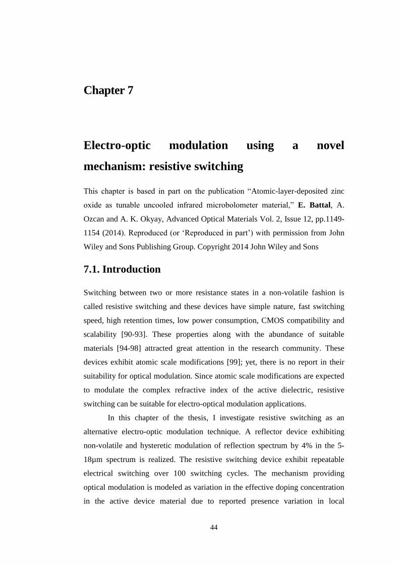
Figure 7.1 – Resistive switching device structure. a) 3-D illustration of the
resistive switching device consisting of a dielectric ZnO film in between an
aluminium and a highly doped Silicon layer (p-type with resistivity of 3.1mΩ-
cm). b) Top view SEM image of the fabricated device. Top aluminium electrode
layer consists of a contact pad region along with digitated fingers for optical
reflection measurements c) TEM cross section image of the device shows 80-
nm-thick ZnO and 120-nm-thick Al layers on top of Si. Copyright 2014 John
Wiley and Sons ...................................................................................................... 45
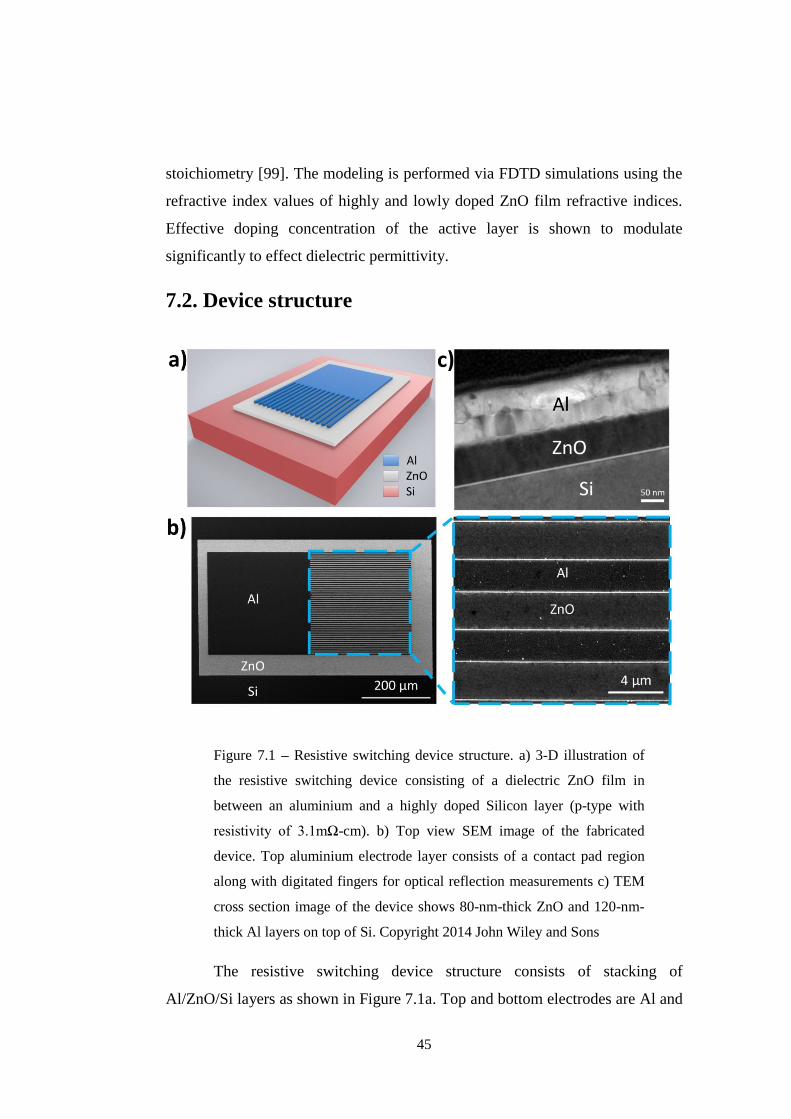
Figure 7.2 – Electrical characteristics of the Al/ZnO/Si resistive switch device
along with TEM images for different memory states. a) I-V characterization of
the device exhibiting more than 100 cycles of resistive switching. b) HRTEM
cross sectional image of the device at LRS depicting thorough filaments from
the top electrode to the bottom. c) When the device switches back to HRS, some
of the filaments partially dissolve and cause increase in the resistivity d) For all
Page 13
xiii
memory states, ohmic conduction with a slope of 1 is present in log-log I-V
curve. Copyright 2014 John Wiley and Sons ........................................................... 47
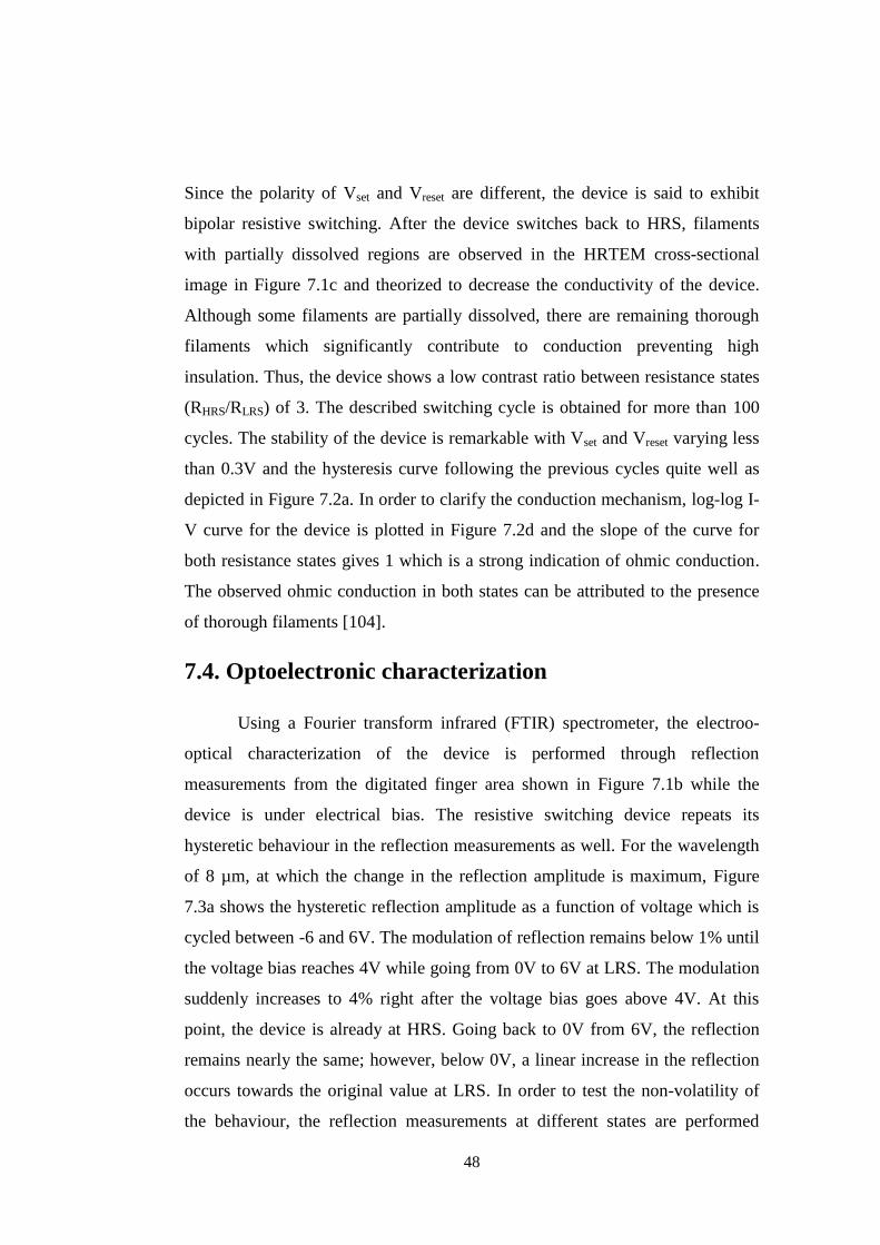
Figure 7.3 – Electro-optic characterization and theoretical modelling of the
device. a) Electro-optic hysteresis behaviour in the reflection spectrum at 8µm
wavelength. b) Broadband non-volatile reflection modulation by 4% in the
entire 5-18µm spectrum c) Extracted modulation of optical constants through
FDTD simulations and modelling the variation of effective doping
concentration between 4.4x10¹⁹
cm-3
and 3.84x10¹⁹
cm-3
d) Simulated reflection
spectra including the effect of modulation of effective doping concentration e)
Strong localization within ZnO dielectric layer in electric field intensity profile
for the wavelength of 14µm. f) Comparably lower localization of the incident
filed in the case for 4µm. Copyright 2014 John Wiley and Sons ............................. 49
Page 14
xiv
List of Tables
Table 5.1 - Cauchy parameters for different ZnO deposition temperatures within
400 - 1700nm spectrum ....................................................................................... 28
Table 5.2 – Both Lorentz and Drude oscillator parameters within the infrared
spectrum of interest as a function of ZnO deposition temperature ..................... 29
Table 6.1 - Thermal dependency of Pole and Cody-Lorentz oscillator parameters for
ZnO in 300 – 1600 nm spectrum. ...................................................................................... 38
Table 6.2 - Thermal dependency of Gaussian oscillator parameters for ZnO in 300 –
1600 nm spectrum. .............................................................................................................. 38
Table 6.3 – IR oscillator parameters for the temperature dependent optical constants of
ZnO………. ........................................................................................................................ 41
Page 15
1
Chapter 1
Introduction
1.1. Plasmonics
Plasmonics is the field investigating the light matter interactions at the
sub-wavelength scale. When the light is incident on a surface with high amount
of free carriers, charge polarization can be induced which can be transformed
into oscillating charges associated with an electromagnetic wave bound to a
surface called surface plasmon. Surface plasmons can provide immense light
localization within a very small surface beyond the limits of conventional
nanophotonics; therefore, enable the way to realize highly resonant optical
devices.
Surface plasmons (SPs) have been tailored to improve the overall device
performance in photovoltaics [1-3] and photo-detection [4-6] applications by
realization of broadband or perfect absorbers. In bio-sensing, frequency
selective resonant surface using SPs have been realized to introduce selectivity
in biologic sample detection [7]. In addition, sensitivity enhancing plasmonic
structures have been introduced for high performance bio-sensing [8]. In solid-
state lighting, surfaces with enhanced scattering cross section have been
achieved using metallic nanoparticles which utilize localized SPs [9, 10]. Metal-
based plasmonic waveguides have been introduced in order to provide chip-to-
chip optical communication in integrated optics applications [11, 12]. Optical
modulators exploiting strong plasmonic resonators have been exploited to push
Page 16
2
the limits in modulation indices [13, 14]. Utilizing the localization properties of
surface plasmons at sub-wavelength scales, nano-lithography below the
diffraction limit has been realized in near-field lithography [15, 16]. The
applications are not only limited to spectral region near the visible and infrared
wavelengths. In the THz and microwave regions of the spectrum, ultra-
broadband radar absorbers [17] as well as wave manipulators [18] have been
realized. Depending on the application requirement, plasmonic structures with
low-loss, high absorbing or high quality factor could be desired and their
realization is highly dependent on the structure geometry as well as material
properties. In this thesis, beam steering as a novel application of plasmonics is
investigated; in addition, a new plasmonic material is introduced.
1.2. Optical modulation schemes
Optical modulators are at the very heart of active light manipulation
technologies. Although the main push for advanced optical modulation
technologies is due to overcome the interconnect bottleneck in current CMOS
technology, recent efforts widened application range to bio-sensing [19],
telecommunications [20], radio frequency and terahertz applications [21]. The
demands for these applications can be listed as fast, high bandwidth, energy
efficient, compact, scalable and integrable modulation technologies. To improve
the manipulation abilities over the optical properties of matter, various number
of modulation schemes utilizing resonant [22] or non-resonant [23] effects have
been put forward. Yet, there is no significant change in the underlying
mechanisms establishing optical modulation. The most common method of
optical modulation is through field induced variation of free carriers within a
semiconductor which would induce refractive index modulation [24]. Another
method is thermo-optic modulation which is highly suitable for monolithic
integration [25]; with additional cost of keeping thermal stability [20]. Among
the alternatives, liquid crystals [26] are known to provide high refractive index
Page 17
3
variations, magneto-optical materials [27] allow fast switching, optically
nonlinear materials [28] enable all optical modulation. However, these methods
induce, additional fabrication costs due to their material-wise hybrid nature. A
recently introduced method is solid-state phase-change [29] technique switching
between metallic and dielectric phases via atomic scale modifications. This
method offers large refractive index variation with fast switching speeds [30],
low switching power [31] and provides non-volatility [30]. The research for
enhancing the modulation performance along with aim for the low-cost and
integration suitability continues. In this thesis, atomic layer deposited ZnO will
be investigated as an alternative high performance dielectric material and a
novel electro-optic modulation mechanism called resistive switching will be
introduced.
1.3. Thesis Overview
In most of the work of this thesis, theoretical calculations based on finite
difference time domain simulations and extraction of optical constants of
dielectric materials via spectroscopic ellipsometry method is performed.
Therefore, these methods will be described in Chapter 2 of this thesis in detail.
In Chapter 3, beam steering is introduced as a novel application of a
plasmonic resonator called metal insulator metal (MIM). Radiation
characteristics of a phased array antenna formed using MIM unit cells is
investigated.
In Chapter 4, a new plasmonic material, InN, is introduced for infrared
applications. Infrared optical characteristics of InN films are investigated and
compared with Au. For proof-of-concept demonstration, a plasmonic infrared
absorber is realized.
Page 18
4
Chapter 5 presents the optical characterization of atomic layer deposited
ZnO for infrared imaging applications. For various deposition temperatures,
ZnO films are characterized through spectroscopic ellipsometry and a reference
device based on this material is investigated and compared with commercially
available counterparts.
In Chapter 6, atomic layer deposited ZnO is investigated as an alternative
thermo-optic modulation material. Thermo-optic coefficients larger than
conventional large band-gap materials have been obtained and a thin film
thermally tunable reflective surface have been realized.
Lastly, in Chapter 7, a novel mechanism electro-optic modulation
mechanism called resistive switching is introduced and investigated in depth.
Electrical and opto-electronic characterization of Al/ZnO/Si resistive switching
device is performed and theoretical calculation of refractive index modulation
by taking the variation in te effective doping concentrations due to modification
of local stoichiometry in the dielectric layer is performed.
Page 19
5
Chapter 2
Methods
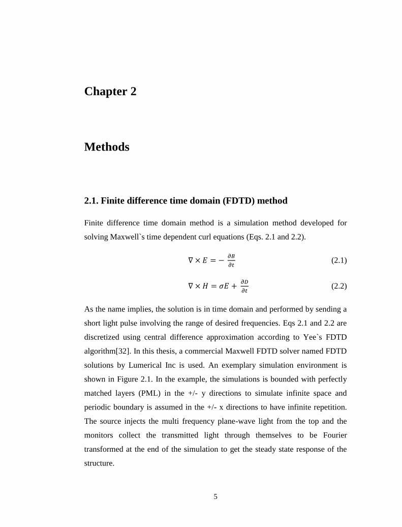
2.1. Finite difference time domain (FDTD) method
Finite difference time domain method is a simulation method developed for
solving Maxwell`s time dependent curl equations (Eqs. 2.1 and 2.2).
∇ × 𝐸 = − 𝜕𝐵
𝜕𝑡 (2.1)
∇ × 𝐻 = 𝜎𝐸 + 𝜕𝐷
𝜕𝑡 (2.2)
As the name implies, the solution is in time domain and performed by sending a
short light pulse involving the range of desired frequencies. Eqs 2.1 and 2.2 are
discretized using central difference approximation according to Yee`s FDTD
algorithm[32]. In this thesis, a commercial Maxwell FDTD solver named FDTD
solutions by Lumerical Inc is used. An exemplary simulation environment is
shown in Figure 2.1. In the example, the simulations is bounded with perfectly
matched layers (PML) in the +/- y directions to simulate infinite space and
periodic boundary is assumed in the +/- x directions to have infinite repetition.
The source injects the multi frequency plane-wave light from the top and the
monitors collect the transmitted light through themselves to be Fourier
transformed at the end of the simulation to get the steady state response of the
structure.
Page 20
6
Figure 2.1 – An exemplary simulation environment
2.2. Spectroscopic ellipsometry
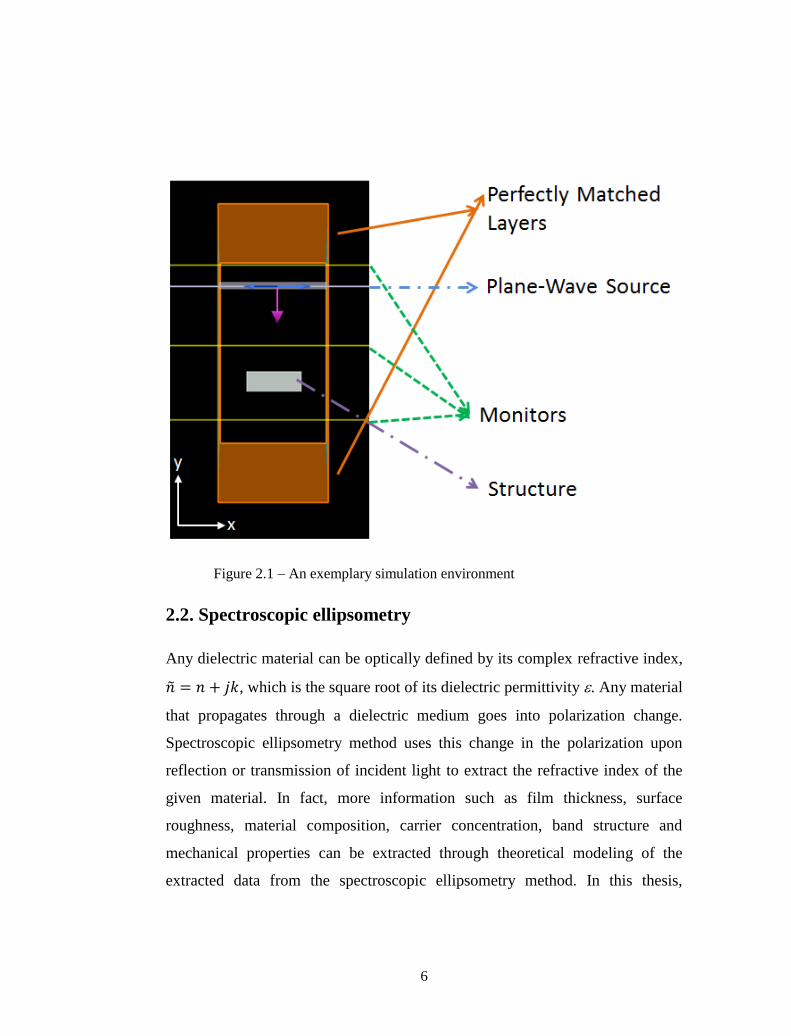
Any dielectric material can be optically defined by its complex refractive index,
= 𝑛 + 𝑗𝑘, which is the square root of its dielectric permittivity . Any material
that propagates through a dielectric medium goes into polarization change.
Spectroscopic ellipsometry method uses this change in the polarization upon
reflection or transmission of incident light to extract the refractive index of the
given material. In fact, more information such as film thickness, surface
roughness, material composition, carrier concentration, band structure and
mechanical properties can be extracted through theoretical modeling of the
extracted data from the spectroscopic ellipsometry method. In this thesis,
Page 21
7
spectroscopic reflection ellipsometry is utilized to extract various properties of
thin films.
A reflected light would undergo polarization change which is described
by complex reflectance ratio
𝜌 = tan(𝛹) 𝑒𝑗𝛥 =𝑟𝑝
𝑟𝑠 (2)
experimentally extracted by measuring Ψ and Δ which are amplitude ratio and
phase shift. In order to measure these parameters, the incident light is passed
through a polarizer to fix the initial polarization to a known state. Then the
polarization of the reflected light is measured by passing through a polarization
matching device set called compensator and analyzer. In order to match to the
polarization of the reflected light the compensator and analyzer rotate which
result in a changing intensity at the detector. This intensity is maximized when
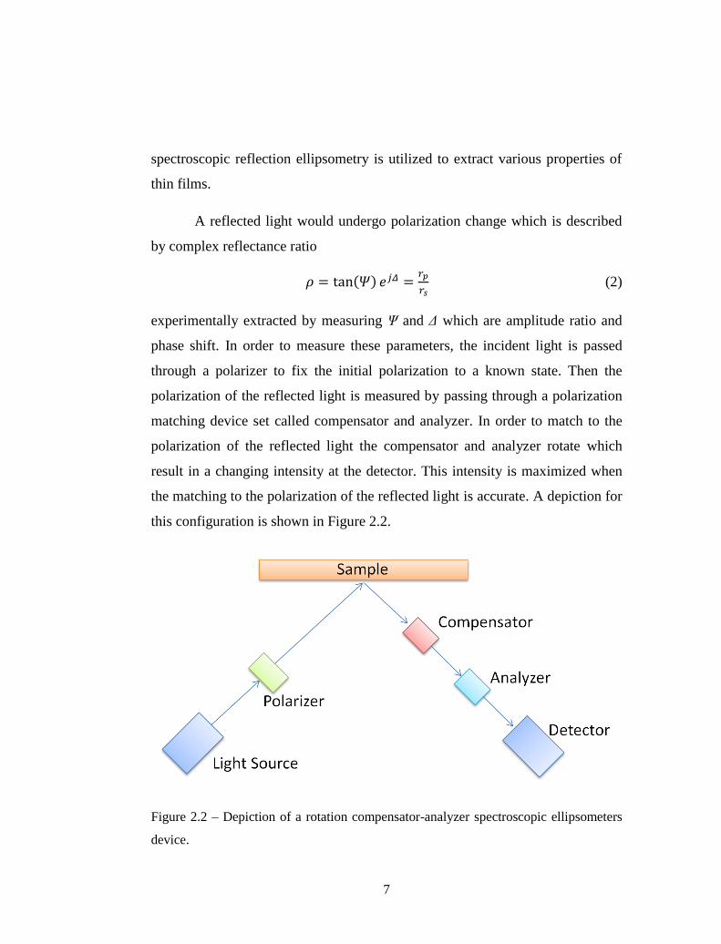
the matching to the polarization of the reflected light is accurate. A depiction for
this configuration is shown in Figure 2.2.
Figure 2.2 – Depiction of a rotation compensator-analyzer spectroscopic ellipsometers
device.
Page 22
8
When the measurement is complete, Ψ/Δ pair is converted to Fresnel reflection
coefficients and fit using oscillator functions modeling the dielectric permittivity
such as Lorentz, Drude, Cody-Lorentz and Gaussian oscillators to determine the
refractive index.
In this thesis the spectroscopic ellipsometry measurements are performed
using commercial ellipsometers V-Vase and IR-Vase by J. A. Woollam Co. for
UV- VIS-NIR and Mid-IR wavelengths, respectively.
Page 23
9
Chapter 3
Metal insulator metal plasmonic infrared beam
steering
This chapter is based in part on the publication “Metal-dielectric-metal
plasmonic resonators for active beam steering in the infrared,” E. Battal, and A.
K. Okyay, Optics Letters Vol. 38, Issue 6, pp.983-985 (2013). Reproduced (or
‘Reproduced in part’) with permission from Optical Society of America
Publishing Group. Copyright 2013 Optical Society of America
3.1 Introduction
Previously, a vast amount of research effort is spent on steering the light beams.
Holographic imaging technologies [33] and novel optical communication schemes [34]
highly depend on controlling the propagation of light in active fashion. Such purposes
lead the researchers to investigate reconfigurable diffraction gratings [35], movable
micro lens arrays [36], tunable waveguides [37], electro-optic prisms [38], and leaky
wave antennas [39]. The dominant technique to achieve non-mechanical beam steering
is active modulation of refractive index. Magneto-optic [40], nonlinear [41], phase
change [42] materials, doped semiconductors [43] and liquid crystals [35] are among
the most commonly used materials for refractive index control. Novel beam steering
devices utilizing surface plasmons (SPs) appeared at operation frequencies of near [44]
and mid [45] infrared wavelengths.
In the literature, metal-insulator-metal (MIM) devices are used to achieve
strong plasmon resonances [46]. Within these devices, surface plasmons propagate at
Page 24
10
the metal insulator interfaces in a coupled fashion resulting in very high localizations
within very small volumes. The optical properties of such devices are shown to be
manipulated using refractive index modulation [46]. With such a property, one can
utilize these devices for the purpose of beam steering.
In this chapter of the thesis, a phased array configuration of MIM plasmonic
resonators operating at mid-infrared wavelengths is formed to realize beam steering.
The radiation pattern of the phased array is investigated to extract the beam steering
characteristics.
3.2. Device structure and simulation setup
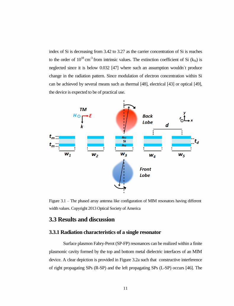
The investigated structure is made of MIM resonators depicted in Figure 3.1.
Due to computational limitations a phased array formed by five individual MIM
resonators is investigated in this work. Each MIM resonator is formed by a dielectric
layer placed in between two metallic layers. The device is assumed to be semi-infinite
in z-direction described in Figure 3.1. To simplify the analysis, dielectric (td) and metal
(tm) thicknesses are taken as 300nm and 100nm, respectively, and the center to center
distance (d) between each MIM resonator is chosen as 2300nm. FDTD method is
performed to analyze the radiation pattern of the structure. A plane-wave like
illumination provided by the total field scattered field source is used to have in phase
excitation of each array element. The illumination is from the top of the structure with a
linear polarization having electric field vector along x-axis to achieve surface plasmon
excitation and the wavelength λ is chosen as 10 µm. Perfectly matched layers boundary
condition is assumed in all directions. A near field to far-field projection technique is
utilized to extract the far field radiation pattern at about 1m which is much higher than
the device dimensions. The dielectric constants for the metal sections of the device are
chosen to be of gold (Au), and the device is assumed to be suspended in air. The
dielectric layer whose refractive index is to be modulated is chosen as Silicon. A widely
used optical constants provided by Palik [47] are used in the simulations. The refractive
Page 25
11
index of Si is decreasing from 3.42 to 3.27 as the carrier concentration of Si is reaches
to the order of 1018
cm-3
from intrinsic values. The extinction coefficient of Si (kSi) is
neglected since it is below 0.032 [47] where such an assumption wouldn t produce
change in the radiation pattern. Since modulation of electron concentration within Si
can be achieved by several means such as thermal [48], electrical [43] or optical [49],
the device is expected to be of practical use.
Figure 3.1 – The phased array antenna like configuration of MIM resonators having different
width values. Copyright 2013 Optical Society of America
3.3 Results and discussion
3.3.1 Radiation characteristics of a single resonator
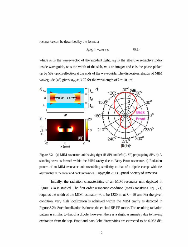
Surface plasmon Fabry-Perot (SP-FP) resonances can be realized within a finite
plasmonic cavity formed by the top and bottom metal dielectric interfaces of an MIM
device. A clear depiction is provided in Figure 3.2a such that constructive interference
of right propagating SPs (R-SP) and the left propagating SPs (L-SP) occurs [46]. The
Page 26
12
resonance can be described by the formula
0
eff
kn w m (5.1)
where k0 is the wave-vector of the incident light, neff is the effective refractive index
inside waveguide, w is the width of the slab, m is an integer and φ is the phase picked
up by SPs upon reflection at the ends of the waveguide. The dispersion relation of MIM
waveguide [46] gives, neff, as 3.72 for the wavelength of λ = 10 µm.
Figure 3.2 - (a) MIM resonator unit having right (R-SP) and left (L-SP) propagating SPs. b) A
standing wave is formed within the MIM cavity due to Fabry-Perot resonance. c) Radiation
pattern of an MIM resonator unit resembling similarity to that of a dipole except with the
asymmetry in the front and back intensities. Copyright 2013 Optical Society of America
Initially, the radiation characteristics of an MIM resonator unit depicted in
Figure 3.2a is studied. The first order resonance condition (m=1) satisfying Eq. (5.1)
requires the width of the MIM resonator, w, to be 1320nm at λ = 10 μm. For the given
condition, very high localization is achieved within the MIM cavity as depicted in
Figure 3.2b. Such localization is due to the excited SP-FP mode. The resulting radiation
pattern is similar to that of a dipole; however, there is a slight asymmetry due to having
excitation from the top. Front and back lobe directivities are extracted to be 0.053 dBi
Page 27
13
and 1.83 dBi, respectively. Half power beam widths (HPBW) of the front and back
lobes are both higher than 150o. As the overall structure is symmetric about y-axis, the
resulting lobes are also symmetric at around y-axis.
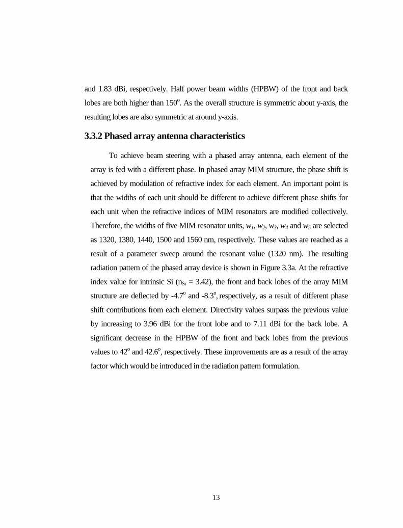
3.3.2 Phased array antenna characteristics
To achieve beam steering with a phased array antenna, each element of the
array is fed with a different phase. In phased array MIM structure, the phase shift is
achieved by modulation of refractive index for each element. An important point is
that the widths of each unit should be different to achieve different phase shifts for
each unit when the refractive indices of MIM resonators are modified collectively.
Therefore, the widths of five MIM resonator units, w1, w2, w3, w4 and w5 are selected
as 1320, 1380, 1440, 1500 and 1560 nm, respectively. These values are reached as a
result of a parameter sweep around the resonant value (1320 nm). The resulting
radiation pattern of the phased array device is shown in Figure 3.3a. At the refractive
index value for intrinsic Si (nSi = 3.42), the front and back lobes of the array MIM
structure are deflected by -4.7o and -8.3
o, respectively, as a result of different phase
shift contributions from each element. Directivity values surpass the previous value
by increasing to 3.96 dBi for the front lobe and to 7.11 dBi for the back lobe. A
significant decrease in the HPBW of the front and back lobes from the previous
values to 42o and 42.6
o, respectively. These improvements are as a result of the array
factor which would be introduced in the radiation pattern formulation.
Page 28
14
Figure 3.3 - (a) The front lobe of the phased array-like MIM structure shifts by 8.75o and the
back lobe shifts by 2.35o when nSi changes by 0.15. b) Normalized radiation intensity (|E|
2n) at
the center of the front lobe shifts continuously and its amplitude increases by decreasing nSi.
Copyright 2013 Optical Society of America
Figure 3.3a depicts the achieved active beam steering by refractive index
modulation. While changing nSi from 3.42 to 3.27, the front lobe steers by 8.75o from
265.25o to 274
o. A continous sweep of nSi results in a continuous beam steering as
shown in Figure 3.3b. The back lobe exhibits poor steering characteristics with a value
of 2.35o. Only a slight change in the HPBW of the front lobe (3.4
o) is observed due to
the modulation of refractive index.
Page 29
15
Figure 3.4 - Magnetic field intensity (|H|2) profile indicates a shift of resonant behavior towards
wider elements (to right) as nSi decreases intermittently from (a) 3.42, to (b) 3.34 and (c) 3.27.
Copyright 2013 Optical Society of America
Extraction of H field intensity profiles shows the phased array like behaviour in
Figure 3.4. From Figure 3.4a to 3.4c, the resonance strength of each resonator unit
changes with the decreasing refractive index value and the resonance strength for each
element is always different for each case indicating introduction of different phase shifts
for the radiated field from these cavities.
Page 30
16
Figure 3.5 - Maximum beam steering angle, Δθmax, is relatively preserved within a full-width
half-maximum of 650nm around the operation wavelength (λ = 10 µm). Copyright 2013
Optical Society of America
Keeping the refractive index of Si the same, the beam steering (Δθmax) for the
front lobe remains the same within a spectral full width half maximum (FWHM) of
650nm between 9.68 – 10.33 µm wavelength range as depicted in Figure 3.5. This
spectrum is highly beneficial for introducing beam steering to commercial CO2 lasers
[50].
3.4. Conclusion
In this section of this thesis, beam steering is achieved utilizing metal-insulator-
metal resonators within a phased array antenna configuration at infrared operation
frequencies. A continuous-angle beam steering of 8.75o
is calculated as a result of
modulation of refractive index of Si by 0.15. A spectral steering bandwidth of 650-nm-
is achieved for the 10m center wavelength. The beam steering is observed to introduce
no modification in the divergence angle of the device. The phased array antenna
concept formed by MIM resonators demonstrated here can be scaled to visible
frequencies as well as THz frequencies.
Page 31
17
Chapter 4
InN based infrared plasmonics
4.1. Introduction
Plasmonics found very wide range of applications covering photovoltaics [51],
photo-detection [6], bio-sensing [52], optical communications [53], surface enhanced
infrared absorption (SEIRA) [54] and Raman spectroscopy [55], infrared and THz
imaging [56]. Most desired material properties for these applications of plasmonics are
low intrinsic loss, CMOS compatibility and bio-compatibility. Noble metals have been
the dominant material for surface plasmon excitation to get high localization of the
incident field. Out of noble metals, gold and silver are considered problematic due to
lack of CMOS compatibility and their relatively high loss. For various applications,
large negative real part of the permittivity is also desired. To satisfy these needs, look
for new plasmonic material has begun recently. Semiconductors with high amount of
free carriers such as Al:ZnO [57], ITO [58], TiN [59] have been considered as good
alternatives fulfilling the necessities. Alternatively, InN with metallic In [60] islands
have attracted attention for the applications within the terahertz spectrum [61]. Yet, this
material is not investigated for applications in infrared spectrum although its high
concentration of electrons makes it viable.
In this chapter of the thesis, optical properties of high-pressure chemical vapor
deposition (HPCVD) grown InN films are investigated for plasmonic application
purposes in the mid-infrared spectrum. An infrared absorber surface with InN is
Page 32
18
realized for proof-of-concept demonstration. In the 3-20μm spectrum, spectroscopic
ellipsometry technique is utilized to extract the optical constants of InN and its surface
plasmon propagation characteristics are compared with that of Au. Strong plasmonic
resonances are obtained by forming corrugated surfaces on an InN film and near perfect
absorption is attained around 14μm wavelength.
4.2. Sample preparation
InN film is deposited on top of GaN/sapphire template. Corresponding
scanning electron micrograph is depicted in Figure 4.1a. The InN film shows
precipitated regions and 3D structures; however, the film can be assumed continuous
with a certain surface roughness using effective medium theory. The device formation
is realized on InN films by patterning via FEI Nova 600i NanoLab focused ion beam
device using Ga+ ions accelerated under 30kV potential with 96pA current. Within 100
x 50 µm2 area corrugations are formed on top of InN films as depicted in Figure 4.1b.
The structural parameters of the corrugations such as depth, width and the period of the
gratings are varied between, 300-900nm, 2-5µm, 5-10µm, respectively, to observe the
effect of grating parameters on the plasmonic response. Strong charge polarization can
be observed with large penetration of the incident field to the corrugations; therefore,
the etching depth is kept at least at 300nm.
Figure 4.1 – Scanning electron microscopy images of a) as grown HPCVD InN
films and b) corrugated plasmonic structures
Page 33
19
4.3. Optical characterization
At angle of incidences of 40° and 55
°, spectroscopic ellipsometry measurements
are carried out in order to obtain the optical properties of the InN films. Then, accurate
modeling of dielectric constant, ε, is performed through spectral fitting of Drude and
Lorentz oscillators which would include the effects of optical phonon modes and free
carriers as well. The corresponding formulation is :
2
2 2 2( ) oD
D L L
D o L
EE A A
E j E E E j E
(8.1)
where ε∞ is the static dielectric permittivity, E is the photon energy, Eo is the
center frequency of the Lorentz oscillator, A and Γ are the oscillator amplitude
and broadening, respectively for the Drude and Lorentz oscillators denoted by D
and L in the subscript, respectively. For the as-grown films, 3.33, 11.42, 81.4,
3.16x10⁻²
eV, 6.28x10⁻³
eV, 5.89x10⁻²
eV, are the values found to best fit ε∞,
AD, AL, ΓD, ΓL and Eo parameters, respectively. The fittings resulted a film
thickness of about 950nm. For the Drude oscillator, the relations A =
(ћμеN)/(εom*) and B = (ће)/(μm
*), where ћ is the Planck’s constant, e is the unit
electronic charge, εo is the free space permittivity, m* is effective mass of
electrons, μ is the electron mobility, N is the carrier concentration, give the
mobility and carrier concentration of InN films as 2.88x10¹⁹
cm-3
and 332.6
cm2/V.s, respectively with m*=0.11mo [62]. The extracted carrier mobility is in
the range of reported values for InN [63]. Figure 4.2a and 4.2b show the
obtained dielectric permittivity values along with that of Au [64] for comparison
purposes. The dielectric constant of InN is lower than that of Au because of the
higher plasma wavelength which is about 3.76μm compared to Au for which it
is in the visible spectrum. The film exhibits phonon-modes centered at 21.05μm,
which effects the dielectric permittivity significantly. The observed phonon
mode is identified as E1TO
[65]. Plasmonic characteristics of InN films have
Page 34
20
been investigated through extraction of propagation length (LP) and mode size
(DW) which indicates field confinement and compare these values with that of
Au using the following relations,
Figure 4.2 – Comparison of optical properties of Au and InN for a) real
and b) imaginary parts of their dielectric permittivity, c) plasmon
propagation length and d) mode size assuming they contact with air
interface.
01/ Im1
mP
m
L k
(8.2)
Page 35
21
ln
air m
W
air m m
m
e
D ee
(8.3)
where 01/ Re 1/ ( 1)air mk , 2
01/ Re / ( 1)m m mk , and k0 is the free space wave-
vector and εm is the dielectric permittivity of the plasmonic material. Figure 4.2c depicts
surface plasmon propagation length along Au/air interface which exceeds that of
InN/air interface by one order of magnitude; whereas InN offers better mode
confinement as depicted in Figure 4.2d. These properties make InN as a good candidate
for plasmonic filter/absorber structure design.
4.4. Device analysis
A representative depiction of the single dimensional plasmonic grooves
patterned on fresh InN films is depicted in Figure 4.3a. In order to verify the extracted
optical constants, fourier transform infrared (FTIR) reflection measurements from the
fresh InN films at normal incidence is performed using Bruker Vertex 70 FTIR
Spectrometer with Hyperion Microscope attachment. The reflection spectra are
compared with simulation results assuming a flat 950-nm-thick InN film FDTD
method. Throughout 3-20μm spectrum a very good agreement between experimental
and theoretical results is achieved and depicted in Figure 4.3b. Slight disagreement at
the higher wavelengths and lower wavelengths is attributed to the surface roughness of
the films. In the un-patterned film optical Fabry Perot resonance is observed for the
quarter-wave film thickness corresponding to the wavelength of 3m in agreement with
the formulation d = mλ/4n for m=1 where d is the thickness of the film, m is the order
of the resonance, n is the refractive index of the film. As a result of this resonance,
strong absorption is observed around the wavelength of resonance.
The excitation of surface plasmons is highly dependent on having charge
polarization along a metal-dielectric interface. For the corrugations formed by InN, the
Page 36
22
incident light should have electric field component perpendicular to the corrugations
(transverse magnetic, TM, polarization) for this purpose. In order to observe surface
plasmon resonance on InN films, the gratings width and period is selected to be 6μm
and 10μm, respectively and the corresponding reflection spectra is depicted in Figure
4.3c. The strength of the resonance can be measured from the strength of the absorption
which is highest at around 14μm. FDTD simulations of the patterned structure is
Figure 4.3 – Device structure with reflection characteristics. a) Representative
image for fresh and corrugated films. b) FTIR reflection spectra of the un-
patterned film agrees well with FDTD simulations c) The patterned grating
structure with the period (P) of 10μm and width (W) of 6μm shows surface
plasmon assisted strong absorption at around 14μm. d) The structure exhibits
plasmon resonance in TM polarization and no- plasmonic resonance at TE
polarization as expected.
performed assuming InN gratings on top of 800nm GaN and c-plane sapphire substrate.
Page 37
23
In-plane optical constants of GaN [66] and c-Sapphire [67] existing in the literature are
used. At the wavelength of strong resonances, the FDTD simulations and FTIR
measurements agree very well in Figure 4.3c. The observed disagreements are
attributed to the imperfections of the InN film which could reflect as higher modes of
resonances or resonance broadening. The corrugated films exhibit polarization
dependent reflection spectra which has a highly resonant plasmonic absorption at TM
spectra and no plasmonic resonance for the TE spectra as expected. Reflection spectra
for the flat film and corrugated film for TE polarization is similar with a slight
difference of magnitude due to loss of light to the transmission spectrum as a result of
light passing through the corrugations.
Figure 4.4 – Electric field intensity profiles for W=6μm, P=10μm, at the
resonant wavelengths of a) λ = 5.5μm and b) 14μm.
In order to investigate the excited plasmon modes within the corrugated films,
the electric field intensity profiles are extracted in Figure 4.4a and b. At λ = 5.5μm, the
corrugated structure exhibits localized surface plasmon resonances around the film
corners which in turn would enhance backward scattering and absorption. Moreover,
the films exhibit strong excitation of propagating surface plasmons on top of InN/air
interface. The excited SP resonance consists of two propagating waves reflected from
the edges of the surface with /2 phase shift. As a result, a constructive interference
Page 38
24
occurs and SP Fabry-Perot resonance arise. The constructive interference equation is
given by m=2nSPW/λ+1/2 where nSP = (εmεd /(εm+ εd))
1/2 is the effective refractive index
for the SP, εd is the dielectric permittivity of the dielectric and m is an integer
representing mode order. Since the dielectric layer is air, εd is 1, the order of mode is
m=3. The arising resonances are not coupled such that there is no interaction between
individual slabs of gratings. However, for the wavelength of 14μm in Figure 4.4b, there
is strong periodic coupling between unit-cells arising from dipolar resonance
excitations. The excited surface plasmon mode can be explained by the grating
momentum matching formula m2/P = 2nSP/λ which matches the momentum
obtained by the scattering due to gratings to that of surface plasmons. For this mode,
effective index approximation is carried out since the resonant field interacts with both
air and GaN layers. From the field profile it is apparent that most of the field is localized
to the 2-μm-thick air region and 0.8-μm-thick GaN film; therefore, εd is found to be
1.43 assuming 2:0.8 air/GaN ratio satisfying the momentum matching of the first order
SP mode (m=1).
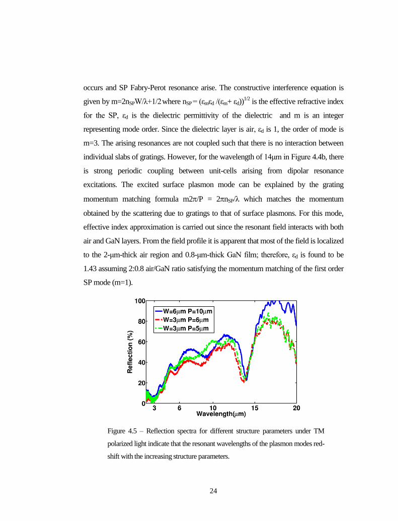
Figure 4.5 – Reflection spectra for different structure parameters under TM
polarized light indicate that the resonant wavelengths of the plasmon modes red-
shift with the increasing structure parameters.
Page 39
25
The effect of structural parameters, W and P, on the plasmon resonances is
explored in Figure 4.5. The location of the surface plasmon resonances do not shift with
the decreasing width of the films significantly as a result of the decreased mode order
around the same wavelengths. Decrease in the periodicity cause small red-shift of the
resonances around 13.9μm to 13.8μmp; whereas, it is slightly higher for the resonance
at 8μm.
4.5. Conclusion
HPCVD grown InN is introduced as an alternative plasmonic material for
infrared applications. Optical properties of the InN films are investigated through
spectroscopic ellipsometry technique within 3-20μm spectrum and observed that InN
exhibits plasmon wavelength below the mid-IR range making it good alternative for
plasmonics applications in the mid-IR range. Plasmon propagation loss and mode
confinement characteristics of InN is compared with that of Au and found out that InN
is better at mode confinement. A strong plasmonic absorber surface supporting more
than one resonant plasmon modes including surface plasmon fabry perot mode and
localized surface plasmon modes is realized. This study demonstrated the viability of
InN as a plasmonic material which makes it suitable for bio-sensing and CMOS
compatible plasmonic applications.
Page 40
26
Chapter 5
Optical characterization of atomic layer deposited
ZnO as a novel bolometric material
This chapter is based in part on the publication “Atomic-layer-deposited zinc
oxide as tunable uncooled infrared microbolometer material,” E. Battal, S.
Bolat, M.Y. Tanrikulu, A. K. Okyay and T. Akin, Physica Status Solidi (a)
applications and materials science Vol. 211, Issue 11, pp.2475-2482 (2014).
Reproduced (or ‘Reproduced in part’) with permission from John Wiley and
Sons Publishing Group. Copyright 2014 John Wiley and Sons
5.1. Introduction
Superior electronic and optical characteristics of ZnO [68, 69] made it
find place within thin film electronics, sensors, and optoelectronics applications.
Its high electron mobility allowed to realize thin film transistors as an alternative
to amorphous Silicon [70, 71]. Due to large band-gap of ZnO, 3.37eV, large
amount of self-doping induced by defects, ZnO has been widely used as a
transparent conducting oxide [72, 73] in addition to an ultraviolet sensor [74].
However, its optical properties within the infrared (IR) region of the spectrum
are not yet fully explored. One candidate application could be infared imaging
where microbolometers are dominant. These devices can operate at room
temperature and low cost, compact, CMOS compatible which make them
preferable over other technologies. Similar to all other type of detectors,
operation of a microbolometer depends on the absorption within an infrared
Page 41
27
sensitive layer. In general, this layer is also used as a structural layer to form the
whole pixel. Most commonly employed material for this purpose is Si3N4 [75].
Currently, a vast amount of research effort is being made to increase the
performance of the present microbolometers. One way of achieving this aim is
to have materials with better absorption performance within the spectrum of
interest.
For the case of ZnO, research on its infrared optical properties which is
very crucial for infrared imaging applications, is very limited. Generally, free
carrier effects and optical phonon modes are the dominant factors defining the
dielectric constant of materials within the IR spectrum. Previously, it has been
shown that pulsed laser deposited ZnO films have phonon modes within 300-
600 cm-1
(~16µm-33µm) spectrum [76]. On the other hand, it has been known
that atomic layer deposited (ALD) ZnO films have large amount of free carriers
whose amount can be controlled via deposition parameters [77]; thus, it is
expected to have free carrier dominant optical properties for ALD grown ZnO
films. ALD grown ZnO is not yet explored as an infrared absorber layer for the
microbolometer application purposes.
In this chapter of the thesis, I explore the optical properties of ALD
grown ZnO and its suitability for microbolometer applications. By modulation
of deposition temperature, the optical characteristics of the deposited films are
modified significantly. In addition, a reference microbolometer design is
proposed and compared with commercially available materials.
5.2. Optical Properties
Spectroscopic ellipsometry method is exploited to extract the optical
properties of atomic layer deposited ZnO. ZnO is known to have an extinction
coefficient (k) close to zero at the wavelengths above its band-edge. For such
Page 42
28
films, Cauchy dispersion model, which is suitable for characterization of
transparent thin films [78], can be used. Initially, this model is employed within
the 400-1700nm spectrum in order to find film thickness. The formulation for
the refractive index and the extinction coefficient in Cauchy dispersion model is
as follows:
𝑛(𝜆) = 𝐴 +𝐵
𝜆2 +𝐶
𝜆4 (6.1)
𝑘(𝜆) = 𝐴𝑘𝑒𝐸𝑘(ℎ𝑐
𝜆−𝐸𝑏)
(6.2)
where A, B, C, Ak and Ek are fit parameters for the model and Eb is the band edge
which is assumed to be 3.37eV. In Table 5.1, the corresponding parameters
resulting the best fit along with the film thicknesses are given.
Growth
Temperature
Thickness
(nm)
A B
[x10-2
]
C
[x10-4
]
Ak
[x10-2
]
Ek
(eV)
80 oC 38.5 1.818 4.37 4.13 4.55 1.73
120 oC 45.5 1.816 5.05 3.92 4.68 1
200 oC 44.9 1.813 4.74 2.84 2.8 0.2
250 oC 34.6 1.786 3.03 2.84 2.18 0.229
Table 5.1 - Cauchy parameters for different ZnO deposition
temperatures within 400 - 1700nm spectrum.
It is known that the infrared spectrum is generally sensitive to free carrier
effects; therefore, the inclusion of free carrier effects is crucial. Drude oscillator
is known to model the effect of free carriers for the measured Ψ/Δ spectrum
obtained via infrared spectroscopic ellipsometry. In order to accurately model
the optical constants within the measured spectrum, 1.8-15µm, a Drude
oscillator along with a Lorentz oscillator is utilized as described in the following
formulation,
𝜀(𝜔) = 𝜀′(𝜔) + 𝑗𝜀′′(𝜔) = 𝜀∞ + 𝜀𝐷𝑟𝑢𝑑𝑒(𝜔) + 𝜀𝐿𝑜𝑟𝑒𝑛𝑡𝑧 (𝜔) (5.3)
Page 43
29
𝜀𝐷𝑟𝑢𝑑𝑒(𝜔) = −𝐴Г
((ħ𝜔)2+𝑗Гħ𝜔) (5.4)
𝜀𝐿𝑜𝑟𝑒𝑛𝑡𝑧 (𝜔) = 𝐴Гħ𝜔𝑛
(ħ𝜔𝑛)2−(ħ𝜔)2−𝑗Гħ𝜔 (5.5)
where ћ is the Planck's constant, ∞ is the static dielectric permittivity, A is the
amplitude of the oscillator, Γ is the broadening, ωn is the center frequency of
the oscillator and ω is the frequency.
The IR optical constants are determined by a least square error algorithm
using the thickness values listed in Table 5.1 assuming the films as isotropic. As
the conductivity of the 80oC grown films is very low, free carrier doesn`t
contribute to dielectric constant significantly; therefore, Drude oscillator is
neglected for this temperature. In Table 5.2, the values resulting the best fit in
parameters of Eqs. (5.3)-(5.5) are listed. The corresponding complex dielectric
constants are plotted in Figure 5.1. The amplitude of the Drude oscillator is
related to the amount of free carriers within the film. Table 5.2 indicates
significant modulation in the amount of free carriers with deposition temperature.
On the other hand, the Lorentz oscillator parameters have relatively low
variance which is attributed to be small variation in the phonon mode properties
of the films by deposition temperature.
Growth
Temperature
∞
Lorentz Drude
A Γ
(cm-1
)
ωn
(cm-1
)
A
(cm-1
)
Γ
(cm-1
)
80 oC 3.70 35.7 47.07 396.5 - -
120 o
C 3.71 51.2 48.3 397.3 1694 8468
200 o
C 3.65 51.6 52.74 397 8109 2024
250 o
C 3.25 55.8 60.98 396.5 14886 2241
Table 5.2 – Both Lorentz and Drude oscillator parameters within the
infrared spectrum of interest as a function of ZnO deposition temperature.
Page 44
30
Figure 5.1 - ALD deposited ZnO optical constants for various deposition
temperatures. (a) Real (') and (b) Imaginary ('') parts of the dielectric
constants of the ALD grown ZnO films is a function of deposition
temperature. Metallic behavior becomes dominant at higher temperatures
due to increased concentration of free carriers. Copyright 2014 John
Wiley and Sons
Absorption properties of the films can be extracted from the imaginary
part of the dielectric constant (''). Increased deposition temperature results in
highly absorptive films which make them suitable for microbolometric
applications as high absorption is desired for the application purposes. There is
also significant control over the real part of the dielectric constant (') by
deposition temperature. The plasma wavelength (p) for the materials, at which
' becomes zero, redshifts for lower deposition temperatures. This indicates
lowering of electron concentration; therefore, conductivity. For 120oC and 80
oC
deposited films, p remains above the wavelength range of interest, noting that
120oC deposited film has higher conductivity compared to 80
oC deposited film
due to having lower ' within the entire spectrum. The plasma wavelength for
Page 45
31
200oC and 250
oC deposited films are 8µm and 4.08µm, respectively; therefore,
these films exhibit metallic behavior which can be exploited for dielectric based
plasmonics in bolometric applications.
In order to verify the optical constants, Fourier transform infrared (FTIR)
reflection spectrum of the as grown ZnO films are measured with respect to the
Si reference such that the spectra would indicate reflection from ZnO surface
divided by reflection from uncoated Si surface. Simulations of the reflection
spectra are performed using the extracted optical constants. The corresponding
results for measurements and simulations, which agree very well, are depicted in
Figure 5.2.
Figure 5.2 – Comparison of FTIR reflection measurements (solid lines)
with simulations (dashed lines) using extracted optical constants. The
agreement between the measured and simulated spectra indicates the
accuracy of the extracted permittivity values. Copyright 2014 John Wiley
and Sons
Page 46
32
5.3. Device Analysis
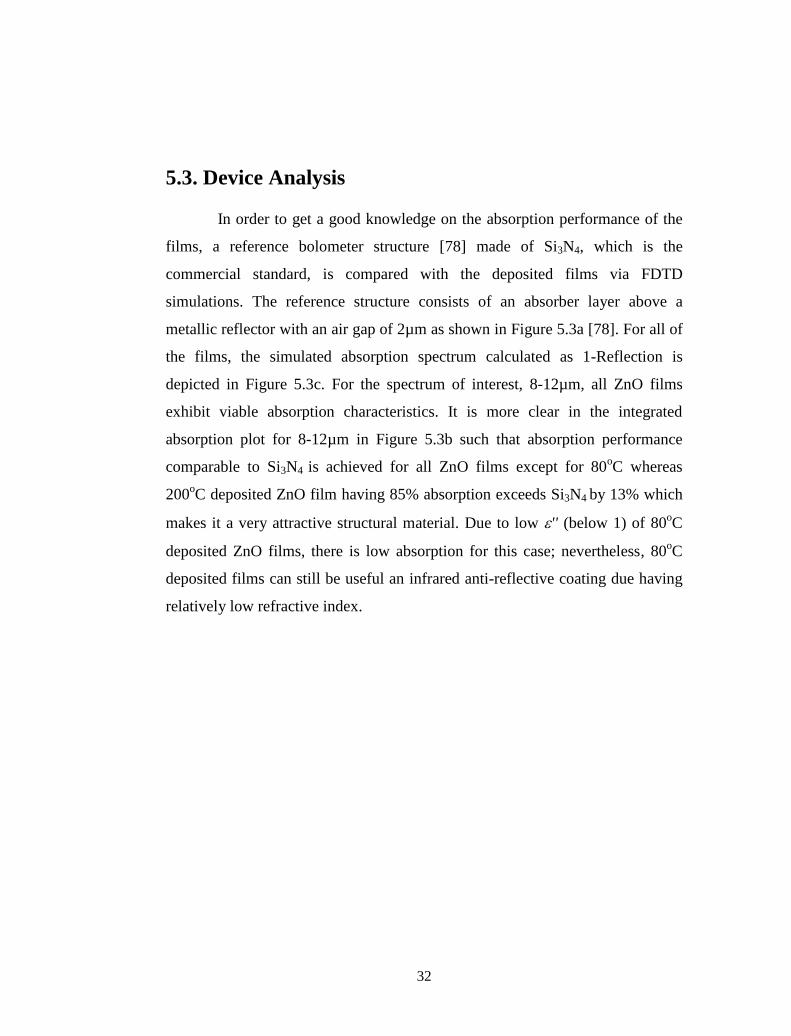
In order to get a good knowledge on the absorption performance of the
films, a reference bolometer structure [78] made of Si3N4, which is the
commercial standard, is compared with the deposited films via FDTD
simulations. The reference structure consists of an absorber layer above a
metallic reflector with an air gap of 2µm as shown in Figure 5.3a [78]. For all of
the films, the simulated absorption spectrum calculated as 1-Reflection is
depicted in Figure 5.3c. For the spectrum of interest, 8-12µm, all ZnO films
exhibit viable absorption characteristics. It is more clear in the integrated
absorption plot for 8-12µm in Figure 5.3b such that absorption performance
comparable to Si3N4 is achieved for all ZnO films except for 80oC whereas
200oC deposited ZnO film having 85% absorption exceeds Si3N4 by 13% which
makes it a very attractive structural material. Due to low '' (below 1) of 80oC
deposited ZnO films, there is low absorption for this case; nevertheless, 80oC
deposited films can still be useful an infrared anti-reflective coating due having
relatively low refractive index.
Page 47
33
Figure 5.3 - Reference structures depiction with absorption
characteristics for different materials. (a) 3D depiction of reference
structure. (b) FDTD simulation of average absorption for both ZnO and
Si3N4 films in 8-12µm spectrum. (c) The spectral absorption for all of
the compared films. Copyright 2014 John Wiley and Sons
5.4. Conclusion
Suitability of optical properties of ALD deposited ZnO films for
bolometric applications is investigated in this chapter. For various deposition
temperature, optical constants of ALD deposited ZnO films are extracted and
modeled utilizing Drude and Lorentz oscillators. Since ALD provides
modulation of free carrier concentrations by variation of deposition temperatures,
the dielectric properties of the films could be manipulated as desired. By
incrementing the deposition temperature, ZnO films with absorption
performance ranging from relatively low to very high can be obtained.
Comparison of the ZnO films with a commercial standard absorber material
indicated that 200oC deposited ZnO films perform much better; therefore,
Page 48
34
become a good candidate for replacing the commercial standard absorber
material in microbolometers.
Page 49
35
Chapter 6
ZnO as an alternative thermo-optic material
6.1 Introduction
The desired control over light matter interactions resulted in birth of
reconfigurable optical structures especially due to expansion of optoelectronic
applications within optical computation and communication, display, lighting, imaging,
holographic technologies. The most dominant methods of optical modulation is
utilization of free-carrier effects, electro-absorption, electro-optic and thermo-optic
effects. However, these effects hit the limits in terms of loss, modulation contrast,
speed, bandwidth, spectral coverage or integration cost; therefore, search for new
schemes has grown. Recently, new optical modulation schemes have been
demonstrated such as coupling metamaterials [22], plasmonic gratings [79], optical
cavities [80] and photonic crystals [81] with well-known optical modulation media i.e.
Silicon [82], GaAs [83], LiNbO3 [84], liquid crystals [85]. On this end, advancements
large band-gap electronics attracted attention in their integration to electro-optical
applications within visible and ultraviolet spectrum.
In this section of the thesis, atomic layer deposited ZnO is introduced as a new
material exhibiting large thermo-optic effects. Active modulation of refractive index is
achieved within the UV-VIS-NIR spectrum and demonstrated via realization of a
Fabry-Perot cavity exhibiting resonant absorption. By modulating the temperature
between 23oC and 200
oC, more than 5nm shift in the resonances within UV-VIS-NIR
spectrum is achieved. Through spectroscopic ellipsometry, temperature dependent
refractive indices of ZnO in 300-1600nm spectrum are extracted. Around the band-
edge of ZnO, largest refractive index modulation is observed and the band-edge is red-
Page 50
36
shifted due to thermal expansion. Optical properties of ZnO is also investigated in mid-
IR spectrum covering 4-40µm and found out that no significant modulation is obtained.
However, the thermal relaxation is verified through the observed red-shift of the optical
phonon modes of ZnO. A thermo-optic coefficient of 9.17x10⁻⁴/oK is obtained around
the band-edge which is the largest among the large band-gap materials
6.2. Ellipsometric Characterization
Ellipsometric measurements are performed in UV-VIS-NIR from a Fabry Perot
resonant cavity structure formed by coating a 240-nm-thick ZnO layer on top of a p-
type silicon wafer with resistivity in the range of 0.1-0.9 Ω-cm. Standard RCA cleaning
procedure is carried out before film deposition. Using atomic layer deposition
technique, ZnO is coated through 1700 deposition cycles within Cambridge Savannah
100 chamber at 250oC.
Prior to the ellipsometric measurements, annealing is carried out on the samples
at 250oC in atmospheric conditions for 90 minutes. A cyclic temperature dependent
ellipsometric measurement is carried out while modulating the sample temperature
between 23oC and 200
oC with illumination at an angle of incidence of 55
o and 57
o. A
nonlinear least square error fitting algorithm is used to fit oscillator parameters to
measured values and the mean square error below 3 is aimed during the fit for all
temperatures. For each temperature of interest, the optical constants of the underlying Si
layer is extracted to eliminate the contribution of refractive index modulation from the
Si layer.
Modeling of optical constants of ZnO is performed using a Cody-Lorentz
oscillator coupled with two Gaussian oscillators and an un-damped Lorentz oscillator.
Cody-Lorentz oscillator is used for accurate modeling of wide-bandgap
semiconductors. The contribution of defect states and intra-band absorptions which
would result in non-zero absorption below the band-gap in the form of an exponentially
decaying function named as Urbach’s Tail [86] is included in this model. The
corresponding equations for the optical constants are as follows
( ) '( ) ''( )E E j E (7.1)
Page 51
37
1 2''( ) '' ( ) '' ( ) '' ( ) '' ( )Cody Lorentz Gauss Gauss PoleE E E E E (7.2)
2 2
2 ''( )'( ) ' ( )PoleE E P d
E
(7.3)
2 2' ( )Pole
o
AE
E E
(7.4)
( )
2
2 2 2 2 2 2 2
1e , ( )
'' ( )( )
, ( )( ) ( )
E Et
Eu
Cody Lorentzg o
g p
EE Eg Et
EE
E E AE EE Eg Et
E E E E E E
(7.5)
2 2ln 4( ) ln 4( )
'' ( )o oE E E
s
E
Gaus A eE e A
(7.6)
Eq. (7.1) separates the real and imaginary part of the complex dielectric function; Eq.
(7.2) is the total imaginary part of the dielectric function which is modeled by various
oscillators listed above; Eq. (7.3) ties the real and imaginary parts of the dielectric
permittivity through Kramers-Kronig relationship; Eqs. (7.4-7.6) describe the oscillator
equations. In these equations, E stands for photon energy, ε∞ is the static dielectric
constant, Eo stands for the center resonance frequency of the oscillator, Γ is the
broadening parameter, A is the oscillator amplitude, Eg is the optical band-gap, Ep is the
transition energy separating absorption onset from Lorentzian behavior, Et is the
transition energy between Urbach tail and band-to-band transitions, Eu is the Urbach
Energy defining the spectral rate of decay of the absorption and E1 is a fit parameter
providing continuity at E=Et. The extracted parameters are given in Tables 6.1 and 6.2
as a function of temperature. Optical band-gap of the ZnO film is found to be 3.23eV at
room-temperature and drops from 3.23eV to 3.10eV for elevation of temperature up to
200oC from 23
oC. This lowering of the band-gap is expected as a result of Varshni`s
formulation [87] which indicates that increased separation between atoms of the
semiconductor as a result of elevated temperature causes narrowing in the band-gap
Page 52
38
Table 6.1 – Thermal dependency of Pole and Cody-Lorentz oscillator
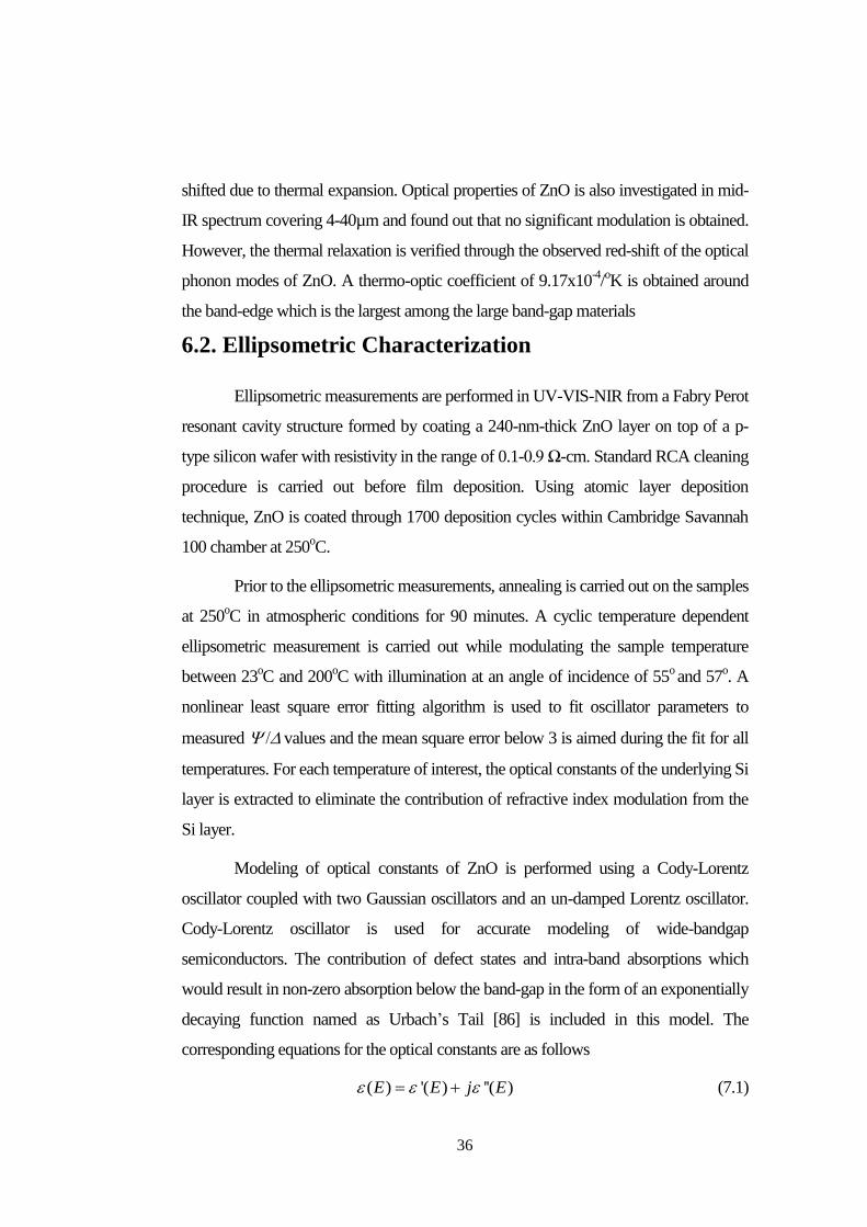
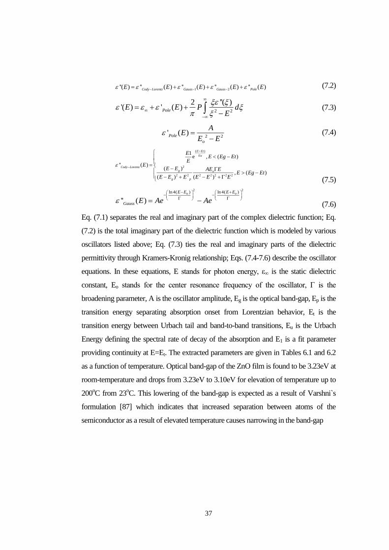
parameters for ZnO in 300 – 1600 nm spectrum.
Table 6.2 - Thermal dependency of Gaussian oscillator parameters for ZnO in
300 – 1600 nm spectrum.
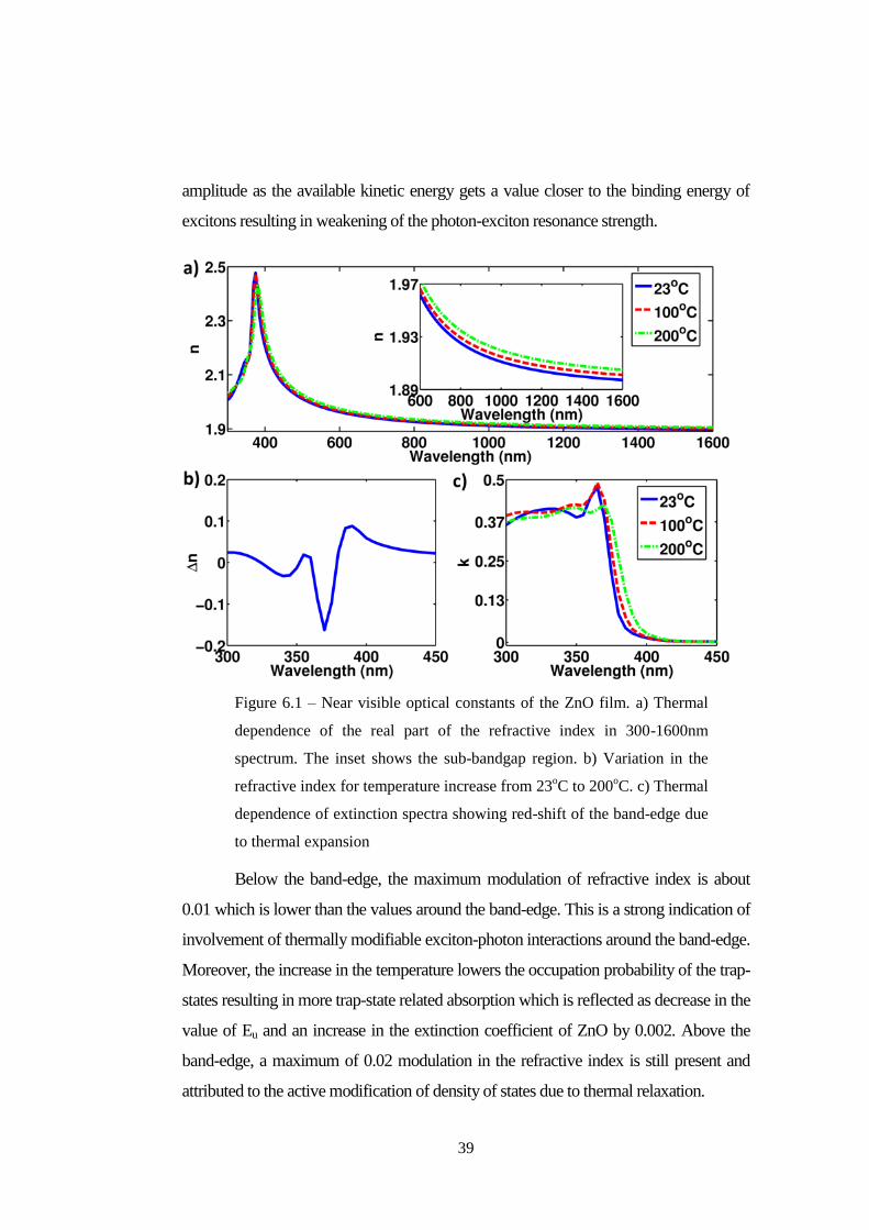
The extracted thermal dependency of refractive index values of ZnO from
Re n in 300-1600nm spectrum is depicted in Figure 6.1a. Both real and
imaginary parts of the refractive index are modulated within the entire spectrum of
interest. Repeatability and volatility of the modulation is verified by observation of
return of ZnO refractive indices to initial values after thermal stress is removed. As
depicted in Figure 6.1b, the refractive index modulation reaches its maximum value of
0.2 at around the band-edge of ZnO which corresponds to a thermo-optic coefficient of
9.17x10⁻⁴/oK exceeding the thermo-optic coefficient of large band-gap semiconductor
counterparts such as AlN, GaN, SiC [88] by 4 times in magnitude.
The exciton binding energy for ZnO is about 60meV which is high enough to
modify the optical properties visibly around the band edge; therefore, a corresponding
sharp peak is observed at the band-edge of the extinction spectra of ZnO in Figure 6.1c.
Increasing temperature causes the excitonic peak to red-shift and get lower in the
ε'Pole ε''Cody-Lorentz
T
(oC)
ε∞ A Eo
(eV)
Γ
(eV)
Eg
(eV)
Ep
(eV)
Et
(eV)
Eu
(eV)
Eo
(eV)
23 2.24 18.3 3.09 0.105 3.26 0.992 0.0102 1.204 5.35
100 2.46 14.8 2.68 0.147 3.16 1.003 0.0181 1.178 5.30
200 2.39 17.8 2.50 0.156 3.10 1.004 0.0191 0.883 5.40
ε''Gauss-1/2
T
(oC)
A Eo
(eV)
Γ
(eV)
23 0.352 / 1.21 3.443 / 3.38 0.405 / 0.140
100 0.777 / 0.944 3.442 / 3.36 0.358 / 0.121
200 0.738 / 0.714 3.424 / 3.32 0.397 / 0.134
Page 53
39
amplitude as the available kinetic energy gets a value closer to the binding energy of
excitons resulting in weakening of the photon-exciton resonance strength.
Figure 6.1 – Near visible optical constants of the ZnO film. a) Thermal
dependence of the real part of the refractive index in 300-1600nm
spectrum. The inset shows the sub-bandgap region. b) Variation in the
refractive index for temperature increase from 23oC to 200
oC. c) Thermal
dependence of extinction spectra showing red-shift of the band-edge due
to thermal expansion
Below the band-edge, the maximum modulation of refractive index is about
0.01 which is lower than the values around the band-edge. This is a strong indication of
involvement of thermally modifiable exciton-photon interactions around the band-edge.
Moreover, the increase in the temperature lowers the occupation probability of the trap-
states resulting in more trap-state related absorption which is reflected as decrease in the
value of Eu and an increase in the extinction coefficient of ZnO by 0.002. Above the
band-edge, a maximum of 0.02 modulation in the refractive index is still present and
attributed to the active modification of density of states due to thermal relaxation.
Page 54
40
Figure 6.2 – IR optical constants of ZnO films. a-b) Real and c-d)
imaginary parts of the mid-infrared anisotropic dielectric constants of
ZnO for in-plane and out-of-plane directions, respectively.
Temperature dependent refractive index of ZnO in mid-IR spectrum
covering 4-40μm is investigated. It is known that optical phonon modes as well
as free-carriers contribute to the dielectric permittivity within this spectrum. To
achieve accurate modeling of these effects, a TO-LO oscillator for phonon
modes is coupled with a Drude oscillator which accounts for the unintentional n-
type doping of ZnO exceeding negligible values, 1016
cm-3
. The polycrystalline
nature of the grown films required to consider anisotropy in the films. The
corresponding equations describing the dielectric function in this range are as
follows
( ) ( ) ( )Drude TO LOE E E (7.7)
2( )Drude E A
E j E
(7.8)
2 2
2 2( ) LO
TO LO
TO
E E j EE A
E E j E
(7.9)
where ELO and ETO stands for the longitudinal and transverse phonon oscillation energy
Page 55
41
The parameters resulting the best fit are given in Table 6.3. To account for the uni-axial
anisotropy, the optical constants are separated into out-of-plane (⊥) and in-plane (∥)
parts. Due to insensitivity of spectroscopic ellipsometry to ETO⊥ and ELO∥ values for the
film thicknesses less than 1μm, literature values are used. A carrier concentration of
1.07x10¹⁹
cm-3
is extracted and agrees well with the literature [89].
Table 6.3 – IR oscillator parameters for the temperature dependent optical
constants of ZnO.
Figure 6.2 shows the permittivity values as a function of temperature for the
infrared region of the spectrum. No significant modulation in the permittivity values are
observed except the region where phonon modes are located, about 27µm. Thermal
expansion of the film causes the in-plane phonon modes to red-shift by 100nm. The
anisotropy of the dielectric constants of the films disappear at the shorter wavelengths
and gets stronger around the wavelengths where phonon modes are located since these
modes are strongly dependent on the direction of the incident field.
6.3. Actively Tunable Surface
By forming a thin optical structure that is comparable to the wavelength of
incidence, a Fabry Perot (FP) resonance can be achieved within an optical cavity. In this
study, the thickness of the ZnO layer is adjusted to achieve constructive interference of
the field within the cavity for which the mechanism is depicted in Figure 6.3a. Using
the following formula, the reflection spectrum can be extracted for the cavity
εDrude εTO-LO
T
(oC)
Anisotropy
Axis
A Γ (eV) A
ELO
(cm-1)
ETO
(cm-1)
Γ
(cm-1)
23
∥ 0.924 0.0664 4.993 590 401.7 34.22
⊥ 0.0669 0.917 6.997 584 378 27.17
200
∥ 0.875 0.0702 4.855 590 397.6 41.48
⊥ 0.0772 0.795 6.824 576.5 378 26.64
Page 56
42
22
1 2 21 2
2 3
R1
ZnO
ZnO
j n kd
j n kd
t t r er
r r e
(6.10)
where r and t corresponds to Fresnel reflection and transmission coefficients at the
corresponding boundaries depicted in Figure 6.3a. For the room temperature (23oC),
Figure 6.3 – Device structure with reflection characteristics as a function
of temperature. a) Depiction of Fabry-Perot resonance mechanism. b)
The measured reflection spectrum at the angle of incidence of 20o and p-
polarization along with the theoretical calculation. c) Thermo-optic
modulation of FP-resonance. d) No significant modulation in mid-IR
regime.
the reflection spectrum in UV-VIS-NIR range for 20o
angle of incidence and p-
polarization is shown in Figure 6.3b along with the theoretical calculation using Eq.
Page 57
43
(6.10) and the extracted optical constants in Figure 6.1a. Using the extracted refractive
indices of ZnO, room temperature FP resonance locations are predicted as 407nm and
610nm which agree well with the experimental results. These wavelengths correspond
to the second and third order FP resonances, formulated by d = (2m+1)(λ/4nZnO) where
m is an integer.
Figure 6.3c shows the reflection spectrum below mid-IR regime as a function
of temperature. More than 5nm resonance shift is observed as a result of thermo-optic
modulation of refractive index. The shift in the spectra around the band-edge is higher,
10nm, despite having no resonance around the band-edge. This observation is as a
result of higher refractive index modulation around the band-edge.
Thermal dependence of the reflection spectrum is also investigated for mid-IR
spectrum at 25o
angle of incidence and the corresponding measurements are plotted in
Figure 6.3d. The spectrum shows the first order FP-resonance partially near 2µm
wavelength. No FP resonance is observed above 2µm wavelength as the structure
dimensions remains below sub-wavelength regime. Only ELO⊥ and ETO∥ phonon modes
located at 17.1µm and 24.9µm, respectively, are observable and red-shift by 100nm in
agreement with the ellipsometric measurements.
6.4. Conclusion
Atomic layer deposited ZnO is investigated as an alternative thermo-optic
material in UV-VIS-NIR-MIR range of the spectrum. Temperature dependent optical
constants of the ZnO film are extracted using spectroscopic ellipsometry. Below the
MIR spectrum, refractive index modulation reached up to 0.2 for a temperature
difference of 177oC which exceeded the values for well known large-band-gap
materials. In MIR spectrum no significant modulation of refractive index is observed
except the region where phonon modes are dominant. The phonon modes are observed
to red-shift by 100nm. As a proof-of-concept, the deposited film is measured as an
actively tunable reflector surface exhibiting more than 5nm spectral shift due to FP
resonances and large refractive index modulation around the band-edge.
Page 58
44
Chapter 7
Electro-optic modulation using a novel
mechanism: resistive switching
This chapter is based in part on the publication “Atomic-layer-deposited zinc
oxide as tunable uncooled infrared microbolometer material,” E. Battal, A.
Ozcan and A. K. Okyay, Advanced Optical Materials Vol. 2, Issue 12, pp.1149-
1154 (2014). Reproduced (or ‘Reproduced in part’) with permission from John
Wiley and Sons Publishing Group. Copyright 2014 John Wiley and Sons
7.1. Introduction
Switching between two or more resistance states in a non-volatile fashion is
called resistive switching and these devices have simple nature, fast switching
speed, high retention times, low power consumption, CMOS compatibility and
scalability [90-93]. These properties along with the abundance of suitable
materials [94-98] attracted great attention in the research community. These
devices exhibit atomic scale modifications [99]; yet, there is no report in their
suitability for optical modulation. Since atomic scale modifications are expected
to modulate the complex refractive index of the active dielectric, resistive
switching can be suitable for electro-optical modulation applications.
In this chapter of the thesis, I investigate resistive switching as an
alternative electro-optic modulation technique. A reflector device exhibiting
non-volatile and hysteretic modulation of reflection spectrum by 4% in the 5-
18µm spectrum is realized. The resistive switching device exhibit repeatable
electrical switching over 100 switching cycles. The mechanism providing
optical modulation is modeled as variation in the effective doping concentration
in the active device material due to reported presence variation in local
Page 59
45
stoichiometry [99]. The modeling is performed via FDTD simulations using the
refractive index values of highly and lowly doped ZnO film refractive indices.
Effective doping concentration of the active layer is shown to modulate
significantly to effect dielectric permittivity.
7.2. Device structure
Figure 7.1 – Resistive switching device structure. a) 3-D illustration of
the resistive switching device consisting of a dielectric ZnO film in
between an aluminium and a highly doped Silicon layer (p-type with
resistivity of 3.1mΩ-cm). b) Top view SEM image of the fabricated
device. Top aluminium electrode layer consists of a contact pad region
along with digitated fingers for optical reflection measurements c) TEM
cross section image of the device shows 80-nm-thick ZnO and 120-nm-
thick Al layers on top of Si. Copyright 2014 John Wiley and Sons
The resistive switching device structure consists of stacking of
Al/ZnO/Si layers as shown in Figure 7.1a. Top and bottom electrodes are Al and
Page 60
46
highly doped p-type Si layers. An island of dielectric ZnO layer is formed to
isolate the device and the top Al layer is patterned to form electrical contact pad
with digitated optical measurement region. The device area is 300x600µm2
and
the corresponding SEM image is shown in Figure 7.1b. The top electrode
consists of two regions, half the contact pad and half the electro-optic region
with gratings having width of 2.43µm and distance of 2.8µm, for which, the
TEM cross sectional image is shown in Figure 7.1c.
7.3. Electrical characterization
Electrical properties of the resistive switching device are characterized
through straightforward current-voltage (I-V) measurements. Electrical bias is
applied from the top electrode while the bottom Si layer is grounded. The
current flow from the fresh devices is on the order of 100μA/cm2. Resistive
switching behavior is achieved via a controlled breakdown process which is
named as electroforming and performed by employing high electrical voltages to
the device. Electroforming allows the resistive switching devices to have atomic
scale modifications such as increase of conductivity of the films due to
formation of filamentary conducting paths via electric field induced redox
reactions [100] and Joule heating [101] as well as zinc and oxygen ion migration
[102]. In order to prevent permanent breakdown of the device, the applied power
is limited through current flow. In this study, electroforming is performed with a
voltage bias of -6V for 1 second duration with a current compliance of 100mA.
Repeatable resistive switching is obtained by applying a dual voltage bias sweep
between -6 and 6V with again 100mA current compliance. As expected from a
resistive switching device, the I-V characteristics of the device shows a
hysteresis loop as depicted in the switching cycle of the device in Figure 7.2a.
The switching cycle starts by having the device stay at high resistance state
(HRS) during the voltage sweep from -6 to 6V until the voltage bias becomes
the set voltage (Vset) of 2.4V. At this point, a sudden increase in the current
amplitude occurs and the device hits to the current compliance going into low
resistance state (LRS). In high-resolution transmission electron microscope
Page 61
47
(HRTEM) images of the device at LRS, Figure 7.2b, there is clear presence of
conducting filaments reaching from the top electrode to the bottom Si substrate,
which are responsible for most of the current flow. The filaments in this figure
have trapezoidal shape which indicates that the mobile oxygen ions move
towards the bottom Si layer during the switching
Figure 7.2 - Electrical characteristics of the Al/ZnO/Si resistive switch
device along with TEM images for different memory states. a) I-V
characterization of the device exhibiting more than 100 cycles of
resistive switching. b) HRTEM cross sectional image of the device at
LRS depicting thorough filaments from the top electrode to the bottom.
c) When the device switches back to HRS, some of the filaments
partially dissolve and cause increase in the resistivity d) For all memory
states, ohmic conduction with a slope of 1 is present in log-log I-V curve.
Copyright 2014 John Wiley and Sons
process [103]. Continuing the voltage sweep from 6 to -6V, the device switches
back to HRS with a sharp decrease in the current at -2.4V reset voltage (Vreset).
Page 62
48
Since the polarity of Vset and Vreset are different, the device is said to exhibit
bipolar resistive switching. After the device switches back to HRS, filaments
with partially dissolved regions are observed in the HRTEM cross-sectional
image in Figure 7.1c and theorized to decrease the conductivity of the device.
Although some filaments are partially dissolved, there are remaining thorough
filaments which significantly contribute to conduction preventing high
insulation. Thus, the device shows a low contrast ratio between resistance states
(RHRS/RLRS) of 3. The described switching cycle is obtained for more than 100
cycles. The stability of the device is remarkable with Vset and Vreset varying less
than 0.3V and the hysteresis curve following the previous cycles quite well as
depicted in Figure 7.2a. In order to clarify the conduction mechanism, log-log I-
V curve for the device is plotted in Figure 7.2d and the slope of the curve for
both resistance states gives 1 which is a strong indication of ohmic conduction.
The observed ohmic conduction in both states can be attributed to the presence
of thorough filaments [104].
7.4. Optoelectronic characterization
Using a Fourier transform infrared (FTIR) spectrometer, the electroo-
optical characterization of the device is performed through reflection
measurements from the digitated finger area shown in Figure 7.1b while the
device is under electrical bias. The resistive switching device repeats its
hysteretic behaviour in the reflection measurements as well. For the wavelength
of 8 µm, at which the change in the reflection amplitude is maximum, Figure
7.3a shows the hysteretic reflection amplitude as a function of voltage which is
cycled between -6 and 6V. The modulation of reflection remains below 1% until
the voltage bias reaches 4V while going from 0V to 6V at LRS. The modulation
suddenly increases to 4% right after the voltage bias goes above 4V. At this
point, the device is already at HRS. Going back to 0V from 6V, the reflection
remains nearly the same; however, below 0V, a linear increase in the reflection
occurs towards the original value at LRS. In order to test the non-volatility of
the behaviour, the reflection measurements at different states are performed
Page 63
49
while the voltage bias is removed and observed that the reflection amplitude
does not change after the bias is removed. Thus, it can be concluded that the
dielectric permittivity of the active layer, ZnO, gets modified in a non-volatile
fashion via resistive switching which provides atomic scale modifications.
Throughout the 5-18µm spectrum, non-volatile modulation of the reflection
spectrum is also observed by 4% for different states under zero electrical bias as
depicted in Figure 7.3b.
Figure 7.3. Electro-optic characterization and theoretical modelling of
the device. a) Electro-optic hysteresis behaviour in the reflection
spectrum at 8µm wavelength. b) Broadband non-volatile reflection
modulation by 4% in the entire 5-18µm spectrum c) Extracted
modulation of optical constants through FDTD simulations and
modelling the variation of effective doping concentration between
Page 64
50
4.4x10¹⁹
cm-3
and 3.84x10¹⁹
cm-3
d) Simulated reflection spectra
including the effect of modulation of effective doping concentration e)
Strong localization within ZnO dielectric layer in electric field intensity
profile for the wavelength of 14µm. f) Comparably lower localization of
the incident filed in the case for 4µm. Copyright 2014 John Wiley and
Sons
Since resistive switching is known to generate modifications in local
stochiometry within an oxide based dielectric [103], in turn, modulate effective
doping concentration of the dielectric [105, 106];, variation of the dielectric
constants is expected [107]. Drude theory of free carriers theorizes that doping
or free carrier concentration affects the optical constants of dielectric especially
known to be effective above the near infrared spectrum [107]. To accurately
look for the effects of modulation of doping concentration, optical constants of
ZnO films with doping concentrations between 1016
cm-3
up to 1021
cm-3
are
extracted. Using these values, FDTD simulations have been performed to fit the
experimental reflection spectrum. During the simulations, available literature
values [108] for the p-type silicon with resistivity of 3.1 mΩ-cm is used. Best
fitting doping concentrations of 3.84x10¹⁹
for HRS and 4.4x10¹⁹
cm-3
for LRS,
for which the refractive index values are plotted in Figure 7.3c. Very good
agreement between the simulation results for the reflection spectrum in Figure
7.3d and that of experimental results in Figure 7.3b. Similar to the experimental
results, 4% modulation in the reflection spectra within 5-18µm spectrum lower
than 1% below 5 µm is. When the field intensity profiles at 4µm and 14µm in
Figure 7.3e and 7.3f, respectively, are investigated, it becomes clear that higher
field localization; therefore, higher interaction, in the active layer at higher
wavelengths makes it more affected by the refractive index modulation due to
resistive switching. The accuracy in the modelling of the modulated reflection
spectrum with the variation in the effective doping concentrations through
FDTD simulations indicates that the local stoichiometry is modified at different
resistance states and therefore the effective doping concentration of the film.
Page 65
51
7.5. Conclusion
Resistive switching is demonstrated as a novel electro-optic modulation
method. A proof-of-concept device is demonstrated via realizing a stack of
Al/ZnO/Si layers exhibiting resistive switching behavior. Using FTIR
measurements while having the device under electrical bias, electro-optical
modulation of reflection spectrum by 4% within 5-18μm spectrum is observed.
The resistive switching mechanism of the device is shown to be formation and
rupture of conductive filamentary regions via TEM images. Taking modification
of local stoichiometry into account, the observed electro-optic modulation is
theoretically modeled through effect of effective doping concentration on
dielectric permittivity. As a result of this study, resistive switching mechanism is
tied with optical modulation schemes as a new method and pave the way for
realizing non-volatile optical memory devices.
Page 66
52
Conclusion
Plasmonics is investigated in terms of novelty in applications and also in
material. A new method of beam steering utilizing a plasmonic resonator called metal-
insulator-metal is introduced. By forming a phased array antenna out of these resonators
with slightly different structural dimensions and controlling the refractive index of the
insulator layer, active beam steering is demonstrated theoretically within the infrared
spectrum. Beam steering range up to 8.75o is achieved by refractive index variation of
about 0.15. Beam steering is not limited to a single frequency but achieved within
650nm spectrum around 10μm wavelength while the beam steering range remains
nearly the same.
Material aspects of plasmonics is explored through demonstration of a new free
carrier rich material, HPCVD grown InN, as a surface plasmon bearing dielectric. Mid-
IR optical constants of InN is extracted using spectroscopic ellipsometry and optical
characteristics as well as surface plasmon characteristics such as plasmon propagation
loss and mode size is investigated and compared with that of Au. A proof-of-concept
plasmonic device made out of InN gratings have been realized to show that a strongly
resonant absorber surface can be achieved with InN supportin various plasmonic
modes.
Investigation of novel materials covers more than half of this thesis.
Atomic layer deposited ZnO films are investigated for micro-bolometric
applications within the infrared region of the spectrum through extraction of the
optical properties of the films at various deposition temperatures. Well-known
Drude and Lorentz oscillators have been utilized while modelling the dielectric
constants of the films and observed that the amount of the free carrier
concentration within the films contribute significantly to the optical properties
and can be modulated via deposition temperature. Thanks to controllable optical
properties of ZnO films, reference bolometer device utilizing this novel material
have been theoretically shown to exceed the integrated absorption performance
of the commercially standard material.
Page 67
53
Then, ZNO films are investigated for their suitability in thermos-optic
applications within the visible and infrared region of the spectrum through, again,
spectroscopic ellipsometry. By modulating the temperature of a ZnO film, the
temperature dependent refractive index of ALD grown ZnO films have been extracted.
A maximum modulation of about 0.2 with only 177oC temperature difference is
achieved and observed to be larger than that of the large-bandgap counterparts in the
near visible range of the spectrum. In the IR range, optical constants indicated red-shift
in the phonon-modes of ZnO as a result of thermal expansion.
Finally, resistive switching, which is modulation of resistance of an
electrical device between different values in a non-volatile fashion, is explored
for opto-electronic applications. An electro-optic modulator is constructed by
stacking Al/ZnO/Si layers which forms a device exhibiting stable resistive
switching. Through reflection measurements under electrical bias, up to 4%
modulation in the reflection spectrum is observed throughout mid-IR spectrum.
Formation and dissolution of the filaments, which modify local stoichiometry,
are observed in TEM studies. Therefore, the modulated refractive index is
modeled as a result of variation in the effective doping concentration and very
good agreement between the theoretical and experimental results is achieved.
Page 68
54
Bibliography
[1] H. A. Atwater and A. Polman, "Plasmonics for improved photovoltaic devices,"
Nat Mater, vol. 9, pp. 205-213, 2010.
[2] S. Pillai and M. A. Green, "Plasmonics for photovoltaic applications," Solar
Energy Materials and Solar Cells, vol. 94, pp. 1481-1486, 2010.
[3] E. Battal, T. A. Yogurt, L. E. Aygun, and A. K. Okyay, "Triangular metallic
gratings for large absorption enhancement in thin film Si solar cells," Optics
Express, vol. 20, pp. 9458-9464, 2012/04/23 2012.
[4] J. A. Shackleford, R. Grote, M. Currie, J. E. Spanier, and B. Nabet, "Integrated
plasmonic lens photodetector," Applied Physics Letters, vol. 94, p. 083501,
2009.
[5] J. Hetterich, G. Bastian, N. A. Gippius, S. G. Tikhodeev, G. von Plessen, and U.
Lemmer, "Optimized Design of Plasmonic MSM Photodetector," Quantum
Electronics, IEEE Journal of, vol. 43, pp. 855-859, 2007.
[6] F. B. Atar, E. Battal, L. E. Aygun, B. Daglar, M. Bayindir, and A. K. Okyay,
"Plasmonically enhanced hot electron based photovoltaic device," Optics
Express, vol. 21, pp. 7196-7201, 2013/03/25 2013.
[7] P. Jain, X. Huang, I. El-Sayed, and M. El-Sayed, "Review of Some Interesting
Surface Plasmon Resonance-enhanced Properties of Noble Metal Nanoparticles
and Their Applications to Biosystems," Plasmonics, vol. 2, pp. 107-118,
2007/09/01 2007.
[8] J. Lakowicz, "Plasmonics in Biology and Plasmon-Controlled Fluorescence,"
Plasmonics, vol. 1, pp. 5-33, 2006/03/01 2006.
[9] G. Lozano, D. J. Louwers, S. R. K. Rodriguez, S. Murai, O. T. A. Jansen, M. A.
Verschuuren, and J. Gomez Rivas, "Plasmonics for solid-state lighting:
enhanced excitation and directional emission of highly efficient light sources,"
Light Sci Appl, vol. 2, p. e66, 2013.
[10] R. M. Bakker, H.-K. Yuan, Z. Liu, V. P. Drachev, A. V. Kildishev, V. M.
Shalaev, R. H. Pedersen, S. Gresillon, and A. Boltasseva, "Enhanced localized
fluorescence in plasmonic nanoantennae," Applied Physics Letters, vol. 92, p.
043101, 2008.
[11] R. F. Oulton, V. J. Sorger, D. A. Genov, D. F. P. Pile, and X. Zhang, "A hybrid
plasmonic waveguide for subwavelength confinement and long-range
propagation," Nat Photon, vol. 2, pp. 496-500, 2008.
[12] J. Grandidier, G. C. des Francs, S. Massenot, A. Bouhelier, L. Markey, J.-C.
Weeber, C. Finot, and A. Dereux, "Gain-Assisted Propagation in a Plasmonic
Waveguide at Telecom Wavelength," Nano Letters, vol. 9, pp. 2935-2939,
2009/08/12 2009.
[13] J. A. Dionne, K. Diest, L. A. Sweatlock, and H. A. Atwater, "PlasMOStor: A
Metal−Oxide−Si Field Effect Plasmonic Modulator," Nano Letters, vol. 9, pp.
897-902, 2009/02/11 2009.
[14] D. Pacifici, H. J. Lezec, and H. A. Atwater, "All-optical modulation by
plasmonic excitation of CdSe quantum dots," Nat Photon, vol. 1, pp. 402-406,
2007.
[15] Y. Kim, S. Kim, H. Jung, E. Lee, and J. W. Hahn, "Plasmonic nano
lithography
 with a high scan speed contact probe," Optics Express,
vol. 17, pp. 19476-19485, 2009/10/26 2009.
Page 69
55
[16] L. Pan, Y. Park, Y. Xiong, E. Ulin-Avila, Y. Wang, L. Zeng, S. Xiong, J. Rho,
C. Sun, D. B. Bogy, and X. Zhang, "Maskless Plasmonic Lithography at 22 nm
Resolution," Sci. Rep., vol. 1, 2011.
[17] A. Noor and Z. Hu. (2010, Metamaterial dual polarised resistive Hilbert curve
array radar absorber. IET Microwaves, Antennas & Propagation 4(6),
667-673. Available: http://digital-
library.theiet.org/content/journals/10.1049/iet-map.2009.0047
[18] M. B. Johnston, "Plasmonics: Superfocusing of terahertz waves," Nat Photon,
vol. 1, pp. 14-15, 2007.
[19] H. Kang, C.-J. Heo, H. C. Jeon, S. Y. Lee, and S.-M. Yang, "Durable
plasmonic cap arrays on flexible substrate with real-time optical tunability for
high-fidelity SERS devices," ACS Applied Materials & Interfaces, vol. 5, pp.
4569-4574, 2013/06/12 2013.
[20] G. T. Reed, G. Mashanovich, F. Y. Gardes, and D. J. Thomson, "Silicon optical
modulators," Nat Photon, vol. 4, pp. 518-526, 2010.
[21] B. Sensale-Rodriguez, R. Yan, M. M. Kelly, T. Fang, K. Tahy, W. S. Hwang, D.
Jena, L. Liu, and H. G. Xing, "Broadband graphene terahertz modulators
enabled by intraband transitions," Nat Commun, vol. 3, p. 780, 2012.
[22] I. M. Pryce, K. Aydin, Y. A. Kelaita, R. M. Briggs, and H. A. Atwater, "Highly
Strained Compliant Optical Metamaterials with Large Frequency Tunability,"
Nano Letters, vol. 10, pp. 4222-4227, 2010/10/13 2010.
[23] R. M. Briggs, I. M. Pryce, and H. A. Atwater, "Compact silicon photonic
waveguide modulator based on the vanadium dioxide metal-insulator phase
transition," Optics Express, vol. 18, pp. 11192-11201, 2010/05/24 2010.
[24] R. A. Soref and B. R. Bennett, "Electrooptical effects in silicon," Quantum
Electronics, IEEE Journal of, vol. 23, pp. 123-129, 1987.
[25] J. Komma, C. Schwarz, G. Hofmann, D. Heinert, and R. Nawrodt, "Thermo-
optic coefficient of silicon at 1550 nm and cryogenic temperatures," Applied
Physics Letters, vol. 101, pp. -, 2012.
[26] J. Pfeifle, L. Alloatti, W. Freude, J. Leuthold, and C. Koos, "Silicon-organic
hybrid phase shifter based on a slot waveguide with a liquid-crystal cladding,"
Optics Express, vol. 20, pp. 15359-15376, 2012/07/02 2012.
[27] V. V. Temnov, "Ultrafast acousto-magneto-plasmonics," Nat Photon, vol. 6, pp.
728-736, 2012.
[28] R. B. Li, L. Deng, and E. W. Hagley, "Fast, all-optical, zero to π continuously
controllable Kerr phase gate," Physical Review Letters, vol. 110, p. 113902,
2013.
[29] Y. Lu, L. Liu, D. Mandler, and P. S. Lee, "High switching speed and coloration
efficiency of titanium-doped vanadium oxide thin film electrochromic devices,"
Journal of Materials Chemistry C, vol. 1, pp. 7380-7386, 2013.
[30] Y. C. Yang, F. Pan, Q. Liu, M. Liu, and F. Zeng, "Fully room-temperature-
fabricated nonvolatile resistive memory for ultrafast and high-density memory
application," Nano Letters, vol. 9, pp. 1636-1643, 2009/04/08 2009.
[31] L. Heng-Yuan, C. Pang-Shiu, W. Ching-Chiun, M. Siddheswar, T. Pei-Jer, L.
Cha-Hsin, L. Lurng-Shehng, and T. Ming-Jinn, "Low-power switching of
nonvolatile resistive memory using hafnium oxide," Japanese Journal of
Applied Physics, vol. 46, p. 2175, 2007.
[32] Y. Kane, "Numerical solution of initial boundary value problems involving
maxwell's equations in isotropic media," Antennas and Propagation, IEEE
Transactions on, vol. 14, pp. 302-307, 1966.
Page 70
56
[33] N. S. Holliman, N. A. Dodgson, G. E. Favalora, and L. Pockett, "Three-
Dimensional Displays: A Review and Applications Analysis," IEEE
Transactions on Broadcasting, vol. 57, pp. 362-371, 2011.
[34] R. Keil, M. Heinrich, F. Dreisow, T. Pertsch, A. Tunnermann, S. Nolte, D. N.
Christodoulides, and A. Szameit, "All-optical routing and switching for three-
dimensional photonic circuitry," Science Reports, vol. 1 2011.
[35] H.-C. Jau, T.-H. Lin, R.-X. Fung, S.-Y. Huang, J. H. Liu, and A. Y. G. Fuh,
"Optically-tunable beam steering grating based on azobenzene doped
cholesteric liquid crystal," Optics Express, vol. 18, pp. 17498-17503, 2010.
[36] M. Holz and W. C. Goltsos, "Agile beam steering using binary optics microlens
arrays," Optical Engineering, vol. 29, pp. 1392-1397, 1990.
[37] M. Jarrahi, R. F. W. Pease, D. A. B. Miller, and T. H. Lee, "Optical switching
based on high-speed phased array optical beam steering," Applied Physics
Letters, vol. 92, pp. 014106-3, 2008.
[38] J. F. Lotspeich, "Electrooptic light-beam deflection," IEEE Spectrum, vol. 5, pp.
45-52, 1968.
[39] Q. Song, S. Campione, O. Boyraz, and F. Capolino, "Silicon-based optical
leaky wave antenna with narrow beam radiation," Optics Express, vol. 19, pp.
8735-8749, 2011.
[40] V. V. Temnov, "Ultrafast acousto-magneto-plasmonics," Nature Photonics, vol.
6, pp. 728-736, 2012.
[41] A. E. Attard, "Analysis of an Optically Controlled Photonic Switch," Applied
Optics, vol. 38, pp. 3239-3248, 1999.
[42] K. Appavoo and R. F. Haglund, "Detecting Nanoscale Size Dependence in
VO2 Phase Transition Using a Split-Ring Resonator Metamaterial," Nano
Letters, vol. 11, pp. 1025-1031, 2011/03/09 2011.
[43] C. Qiu, X. Ye, R. Soref, L. Yang, and Q. Xu, "Demonstration of reconfigurable
electro-optical logic with silicon photonic integrated circuits," Optics Letters,
vol. 37, pp. 3942-3944, 2012.
[44] D. de Ceglia, M. A. Vincenti, and M. Scalora, "Wideband plasmonic beam
steering in metal gratings," Optics Letters, vol. 37, pp. 271-273, 2012.
[45] D. C. Adams, S. Thongrattanasiri, T. Ribaudo, V. A. Podolskiy, and D.
Wasserman, "Plasmonic mid-infrared beam steering," Applied Physics Letters,
vol. 96, pp. 201112-3, 2010.
[46] S. I. Bozhevolnyi and T. Søndergaard, "General properties of slow-plasmon
resonant nanostructures: nano-antennas and resonators," Optics Express, vol. 15,
pp. 10869-10877, 2007.
[47] E. D. Palik, Handbook of Optical Constants of Solids vol. 3. Orlando:
Academic Press, 1985.
[48] G. Cocorullo, M. Iodice, and I. Rendina, "All-silicon Fabry-Perot modulator
based on the thermo-optic effect," Optics Letters, vol. 19, pp. 420-422, 1994.
[49] Q. Xu and M. Lipson, "All-optical logic based on silicon micro-ring
resonators," Optics Express, vol. 15, pp. 924-929, 2007.
[50] A. Laser. CO2 Molecular Radiation & Typical Tunable Laser Spectrum.
Available: http://www.accesslaserco.com/pdf/CO2 Spectrum and Tunable
Lasers.pdf
[51] H. A. Atwater and A. Polman, "Plasmonics for improved photovoltaic devices,"
Nature Materials, vol. 9, pp. 205-213, 2010.
[52] M. Piliarik and J. í. Homola, "Surface plasmon resonance (SPR) sensors:
approaching their limits?," Optics Express, vol. 17, pp. 16505-16517,
2009/09/14 2009.
Page 71
57
[53] J. Kyung-Young, F. L. Teixeira, and R. M. Reano, "Au/SiO<sub>2</sub>
Nanoring Plasmon Waveguides at Optical Communication Band," Lightwave
Technology, Journal of, vol. 25, pp. 2757-2765, 2007.
[54] K. Chen, R. Adato, and H. Altug, "Dual-Band Perfect Absorber for
Multispectral Plasmon-Enhanced Infrared Spectroscopy," ACS Nano, vol. 6, pp.
7998-8006, 2012/09/25 2012.
[55] S. Ayas, H. Güner, B. Türker, O. Ö. Ekiz, F. Dirisaglik, A. K. Okyay, and A.
Dâna, "Raman Enhancement on a Broadband Meta-Surface," ACS Nano, vol. 6,
pp. 6852-6861, 2012/08/28 2012.
[56] D. Wu, N. Fang, C. Sun, X. Zhang, W. J. Padilla, D. N. Basov, D. R. Smith,
and S. Schultz, "Terahertz plasmonic high pass filter," Applied Physics Letters,
vol. 83, pp. 201-203, 2003.
[57] G. V. Naik, J. Liu, A. V. Kildishev, V. M. Shalaev, and A. Boltasseva,
"Demonstration of Al:ZnO as a plasmonic component for near-infrared
metamaterials," Proceedings of the National Academy of Sciences, vol. 109, pp.
8834-8838, June 5, 2012 2012.
[58] S. Franzen, "Surface Plasmon Polaritons and Screened Plasma Absorption in
Indium Tin Oxide Compared to Silver and Gold," The Journal of Physical
Chemistry C, vol. 112, pp. 6027-6032, 2008/04/01 2008.
[59] G. V. Naik, J. L. Schroeder, X. Ni, A. V. Kildishev, T. D. Sands, and A.
Boltasseva, "Titanium nitride as a plasmonic material for visible and near-
infrared wavelengths," Optical Materials Express, vol. 2, pp. 478-489,
2012/04/01 2012.
[60] T.-T. Kang, A. Hashimoto, and A. Yamamoto, "Optical properties of InN
containing metallic indium," Applied Physics Letters, vol. 92, pp. -, 2008.
[61] T. V. Shubina, N. A. Gippius, V. A. Shalygin, A. V. Andrianov, and S. V.
Ivanov, "Terahertz radiation due to random grating coupled surface plasmon
polaritons," Physical Review B, vol. 83, p. 165312, 2011.
[62] K. Kim, W. R. L. Lambrecht, and B. Segall, "Elastic constants and related
properties of tetrahedrally bonded BN, AlN, GaN, and InN," Physical Review B,
vol. 53, pp. 16310-16326, 1996.
[63] A. G. Bhuiyan, A. Hashimoto, and A. Yamamoto, "Indium nitride (InN): A
review on growth, characterization, and properties," Journal of Applied Physics,
vol. 94, pp. 2779-2808, 2003.
[64] R. L. Olmon, B. Slovick, T. W. Johnson, D. Shelton, S.-H. Oh, G. D. Boreman,
and M. B. Raschke, "Optical dielectric function of gold," Physical Review B,
vol. 86, p. 235147, 2012.
[65] J. S. Dyck, K. Kim, S. Limpijumnong, W. R. L. Lambrecht, K. Kash, and J. C.
Angus, "Identification of Raman-active phonon modes in oriented platelets of
InN and polycrystalline InN," Solid State Communications, vol. 114, pp. 355-
360, 2000.
[66] A. Kasic, M. Schubert, S. Einfeldt, D. Hommel, and T. E. Tiwald, "Free-carrier
and phonon properties of <i>n</i>- and <i>p</i>-type hexagonal GaN films
measured by infrared ellipsometry," Physical Review B, vol. 62, pp. 7365-7377,
2000.
[67] M. Schubert, T. E. Tiwald, and C. M. Herzinger, "Infrared dielectric anisotropy
and phonon modes of sapphire," Physical Review B, vol. 61, pp. 8187-8201,
2000.
[68] G. D. Yuan, W. J. Zhang, J. S. Jie, X. Fan, J. X. Tang, I. Shafiq, Z. Z. Ye, C. S.
Lee, and S. T. Lee, "Tunable n-Type Conductivity and Transport Properties of
Page 72
58
Ga-doped ZnO Nanowire Arrays," Advanced Materials, vol. 20, pp. 168-173,
2008.
[69] Ü. Özgür, Y. I. Alivov, C. Liu, A. Teke, M. A. Reshchikov, S. Doğan, V.
Avrutin, S.-J. Cho, and H. Morkoç, "A comprehensive review of ZnO materials
and devices," Journal of Applied Physics, vol. 98, p. 041301, 2005.
[70] E. M. C. Fortunato, P. M. C. Barquinha, A. C. M. B. G. Pimentel, A. M. F.
Gonçalves, A. J. S. Marques, L. M. N. Pereira, and R. F. P. Martins, "Fully
Transparent ZnO Thin-Film Transistor Produced at Room Temperature,"
Advanced Materials, vol. 17, pp. 590-594, 2005.
[71] R. L. Hoffman, B. J. Norris, and J. F. Wager, "ZnO-based transparent thin-film
transistors," Applied Physics Letters, vol. 82, pp. 733-735, 2003.
[72] E. Klaus, "Magnetron sputtering of transparent conductive zinc oxide: relation
between the sputtering parameters and the electronic properties," Journal of
Physics D: Applied Physics, vol. 33, p. R17, 2000.
[73] A. Yamada, B. Sang, and M. Konagai, "Atomic layer deposition of ZnO
transparent conducting oxides," Applied Surface Science, vol. 112, pp. 216-222,
1997.
[74] Z. K. Tang, G. K. L. Wong, P. Yu, M. Kawasaki, A. Ohtomo, H. Koinuma, and
Y. Segawa, "Room-temperature ultraviolet laser emission from self-assembled
ZnO microcrystallite thin films," Applied Physics Letters, vol. 72, pp. 3270-
3272, 1998.
[75] A. Rogalski, "Infrared detectors: an overview," Infrared Physics & Technology,
vol. 43, pp. 187-210, 2002.
[76] S. Heitsch, C. Bundesmann, G. Wagner, G. Zimmermann, A. Rahm, H.
Hochmuth, G. Benndorf, H. Schmidt, M. Schubert, M. Lorenz, and M.
Grundmann, "Low temperature photoluminescence and infrared dielectric
functions of pulsed laser deposited ZnO thin films on silicon," Thin Solid Films,
vol. 496, pp. 234-239, 2006.
[77] S. J. Lim, S.-j. Kwon, H. Kim, and J.-S. Park, "High performance thin film
transistor with low temperature atomic layer deposition nitrogen-doped ZnO,"
Applied Physics Letters, vol. 91, p. 183517, 2007.
[78] O. Erturk, E. Battal, S. E. Kucuk, A. K. Okyay, and T. Akin, "A plasmonically
enhanced pixel structure for uncooled microbolometer detectors," 2013, pp.
87041E-87041E-7.
[79] Y. J. Liu, Y. B. Zheng, J. Liou, I. K. Chiang, I. C. Khoo, and T. J. Huang, "All-
Optical Modulation of Localized Surface Plasmon Coupling in a Hybrid
System Composed of Photoswitchable Gratings and Au Nanodisk Arrays," The
Journal of Physical Chemistry C, vol. 115, pp. 7717-7722, 2011/04/21 2011.
[80] Z. Zheng, G. Yang, H. Li, and X. Liu, "Three-stage Fabry–Perot liquid
crystal tunable filter with extended spectral range," Optics Express, vol. 19, pp.
2158-2164, 2011/01/31 2011.
[81] D. Sridharan, R. Bose, H. Kim, G. S. Solomon, and E. Waks, "A reversibly
tunable photonic crystal nanocavity laser using photochromic thin film," Optics
Express, vol. 19, pp. 5551-5558, 2011/03/14 2011.
[82] P. Dong, S. Liao, H. Liang, R. Shafiiha, D. Feng, G. Li, X. Zheng, A. V.
Krishnamoorthy, and M. Asghari, "Submilliwatt, ultrafast and broadband
electro-optic silicon switches," Optics Express, vol. 18, pp. 25225-25231,
2010/11/22 2010.
[83] J. r. B. Kinzel, D. Rudolph, M. Bichler, G. Abstreiter, J. J. Finley, G.
Koblmüller, A. Wixforth, and H. J. Krenner, "Directional and Dynamic
Modulation of the Optical Emission of an Individual GaAs Nanowire Using
Page 73
59
Surface Acoustic Waves," Nano Letters, vol. 11, pp. 1512-1517, 2011/04/13
2011.
[84] R. Takigawa, E. Higurashi, T. Suga, and T. Kawanishi, "Air-gap structure
between integrated LiNbO3 optical modulators and micromachined Si
substrates," Optics Express, vol. 19, pp. 15739-15749, 2011/08/15 2011.
[85] I. Moreno, J. A. Davis, T. M. Hernandez, D. M. Cottrell, and D. Sand,
"Complete polarization control of light from a liquid crystal spatial light
modulator," Optics Express, vol. 20, pp. 364-376, 2012/01/02 2012.
[86] M. A. Jacobson, O. V. Konstantinov, D. K. Nelson, S. O. Romanovskii, and Z.
Hatzopoulos, "Absorption spectra of GaN: film characterization by Urbach
spectral tail and the effect of electric field," Journal of Crystal Growth, vol. 230,
pp. 459-461, 2001.
[87] V. Alex, S. Finkbeiner, and J. Weber, "Temperature dependence of the indirect
energy gap in crystalline silicon," Journal of Applied Physics, vol. 79, pp.
6943-6946, 1996.
[88] W. Naoki, K. Tsunenobu, and S. Jun, "Thermo-Optic Coefficients of 4H-SiC,
GaN, and AlN for Ultraviolet to Infrared Regions up to 500 °C," Japanese
Journal of Applied Physics, vol. 51, p. 112101, 2012.
[89] S. J. Lim, S. Kwon, and H. Kim, "ZnO thin films prepared by atomic layer
deposition and rf sputtering as an active layer for thin film transistor," Thin
Solid Films, vol. 516, pp. 1523-1528, 2008.
[90] M.-J. Lee, C. B. Lee, D. Lee, S. R. Lee, M. Chang, J. H. Hur, Y.-B. Kim, C.-J.
Kim, D. H. Seo, S. Seo, U. I. Chung, I.-K. Yoo, and K. Kim, "A fast, high-
endurance and scalable non-volatile memory device made from asymmetric
Ta2O5−x/TaO2−x bilayer structures," Nat Mater, vol. 10, pp. 625-630, 2011.
[91] H. Akinaga and H. Shima, "Resistive random access memory (ReRAM) based
on metal oxides," Proceedings of the IEEE, vol. 98, pp. 2237-2251, 2010.
[92] S. H. Jo and W. Lu, "CMOS compatible nanoscale nonvolatile resistance
switching memory," Nano Letters, vol. 8, pp. 392-397, 2008/02/01 2008.
[93] S. Yu, H.-Y. Chen, B. Gao, J. Kang, and H. S. P. Wong, "HfOx-based vertical
resistive switching random access memory suitable for bit-cost-effective three-
dimensional cross-point architecture," ACS Nano, vol. 7, pp. 2320-2325,
2013/03/26 2013.
[94] B. Choi, J. J. Yang, M. X. Zhang, K. Norris, D. A. Ohlberg, N. Kobayashi, G.
Medeiros-Ribeiro, and R. S. Williams, "Nitride memristors," Applied Physics A,
vol. 109, pp. 1-4, 2012/10/01 2012.
[95] A. Geresdi, M. Csontos, A. Gubicza, A. Halbritter, and G. Mihaly, "A fast
operation of nanometer-scale metallic memristors: highly transparent
conductance channels in Ag2S devices," Nanoscale, vol. 6, pp. 2613-2617,
2014.
[96] B. F. Bory, H. L. Gomes, R. A. J. Janssen, D. M. de Leeuw, and S. C. J.
Meskers, "Role of hole injection in electroforming of LiF-polymer memory
diodes," The Journal of Physical Chemistry C, vol. 116, pp. 12443-12447,
2012/06/14 2012.
[97] L. Wootae, P. Jubong, S. Myungwoo, L. Joonmyoung, J. Seungjae, K.
Seonghyun, P. Sangsu, S. Jungho, and H. Hyunsang, "Excellent state stability
of Cu/SiC/Pt programmable metallization cells for nonvolatile memory
applications," Electron Device Letters, IEEE, vol. 32, pp. 680-682, 2011.
[98] S. Balasubramanian, V. Kumar, N. Balasubramanian, and V. Premachandran,
"Resistance switching in indium phosphide using hydrogen passivation of
acceptors," Applied Physics Letters, vol. 64, pp. 2256-2257, 1994.
Page 74
60
[99] R. Waser and M. Aono, "Nanoionics-based resistive switching memories," Nat
Mater, vol. 6, pp. 833-840, 2007.
[100] R. Waser, R. Dittmann, G. Staikov, and K. Szot, "Redox-based resistive
switching memories – nanoionic mechanisms, prospects, and challenges,"
Advanced Materials, vol. 21, pp. 2632-2663, 2009.
[101] U. Russo, D. Ielmini, C. Cagli, and A. L. Lacaita, "Self-accelerated thermal
dissolution model for reset programming in unipolar resistive-switching
memory (RRAM) devices," Electron Devices, IEEE Transactions on, vol. 56,
pp. 193-200, 2009.
[102] R. Yang, K. Terabe, G. Liu, T. Tsuruoka, T. Hasegawa, J. K. Gimzewski, and
M. Aono, "On-demand nanodevice with electrical and neuromorphic
multifunction realized by local ion migration," ACS Nano, vol. 6, pp. 9515-
9521, 2012/11/27 2012.
[103] D.-H. Kwon, K. M. Kim, J. H. Jang, J. M. Jeon, M. H. Lee, G. H. Kim, X.-S. Li,
G.-S. Park, B. Lee, S. Han, M. Kim, and C. S. Hwang, "Atomic structure of
conducting nanofilaments in TiO2 resistive switching memory," Nat Nano, vol.
5, pp. 148-153, 2010.
[104] K. M. Kim, B. J. Choi, Y. C. Shin, S. Choi, and C. S. Hwang, "Anode-interface
localized filamentary mechanism in resistive switching of TiO2 thin films,"
Applied Physics Letters, vol. 91, pp. -, 2007.
[105] K. Hoffmann and D. Hahn, "Electron spin resonance of lattice defects in zinc
oxide," physica status solidi (a), vol. 24, pp. 637-648, 1974.
[106] A. Pöppl and G. Völkel, "ESR and photo-ESR investigations of zinc vacancies
and interstitial oxygen ions in undoped ZnO ceramics," physica status solidi (a),
vol. 125, pp. 571-581, 1991.
[107] C. A. Wolden, T. M. Barnes, J. B. Baxter, and E. S. Aydil, "Infrared detection
of hydrogen-generated free carriers in polycrystalline ZnO thin films," Journal
of Applied Physics, vol. 97, pp. -, 2005.
[108] S. Basu, B. J. Lee, and Z. M. Zhang, "Infrared radiative properties of heavily
doped silicon at room temperature," Journal of Heat Transfer, vol. 132, pp.
023301-023301, 2009.