11
Public Information GaN Transistors Are Here Faster, Smaller, and More Efficient...
| Date post: | 08-Aug-2015 |
| Category: |
Technology |
| Upload: | on-semiconductor |
| View: | 80 times |
| Download: | 1 times |
Public Information
GaN Transistors Are Here
Faster, Smaller, and More Efficient...
Public Information2 04/15/2023
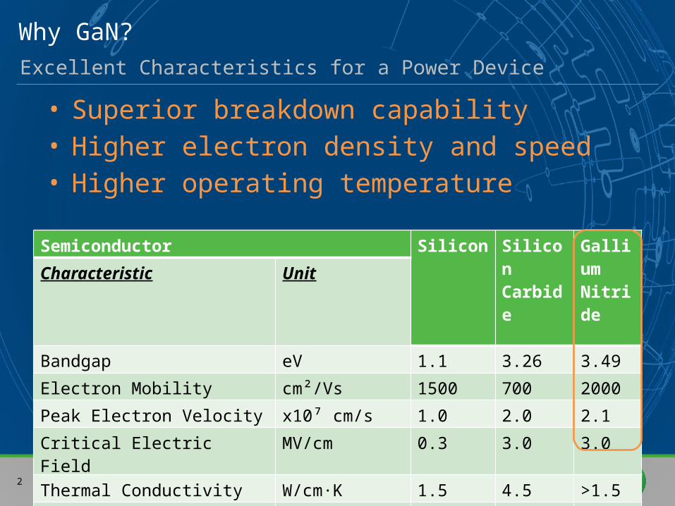
Semiconductor Silicon Silicon Carbide
Gallium Nitride
Characteristic Unit
Bandgap eV 1.1 3.26 3.49
Electron Mobility cm²/Vs 1500 700 2000
Peak Electron Velocity x10⁷ cm/s 1.0 2.0 2.1
Critical Electric Field MV/cm 0.3 3.0 3.0
Thermal Conductivity W/cm·K 1.5 4.5 >1.5
Relative Dielectric Constant
ετ 11.8 10.0 9.0
Why GaN?Excellent Characteristics for a Power Device
• Superior breakdown capability• Higher electron density and speed• Higher operating temperature
Public Information3 04/15/2023
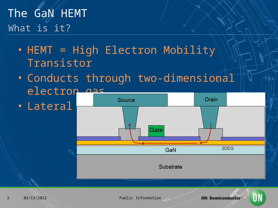
• HEMT = High Electron Mobility Transistor• Conducts through two-dimensional
electron gas• Lateral current conduction
The GaN HEMTWhat is it?
Public Information4 04/15/2023
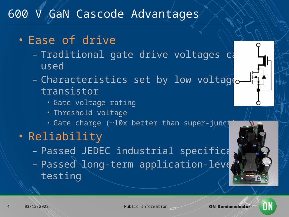
• Ease of drive– Traditional gate drive voltages can be used– Characteristics set by low voltage transistor
• Gate voltage rating• Threshold voltage• Gate charge (~10x better than super-junction)
• Reliability– Passed JEDEC industrial specifications– Passed long-term application-level testing
600 V GaN Cascode Advantages
Public Information5 04/15/2023
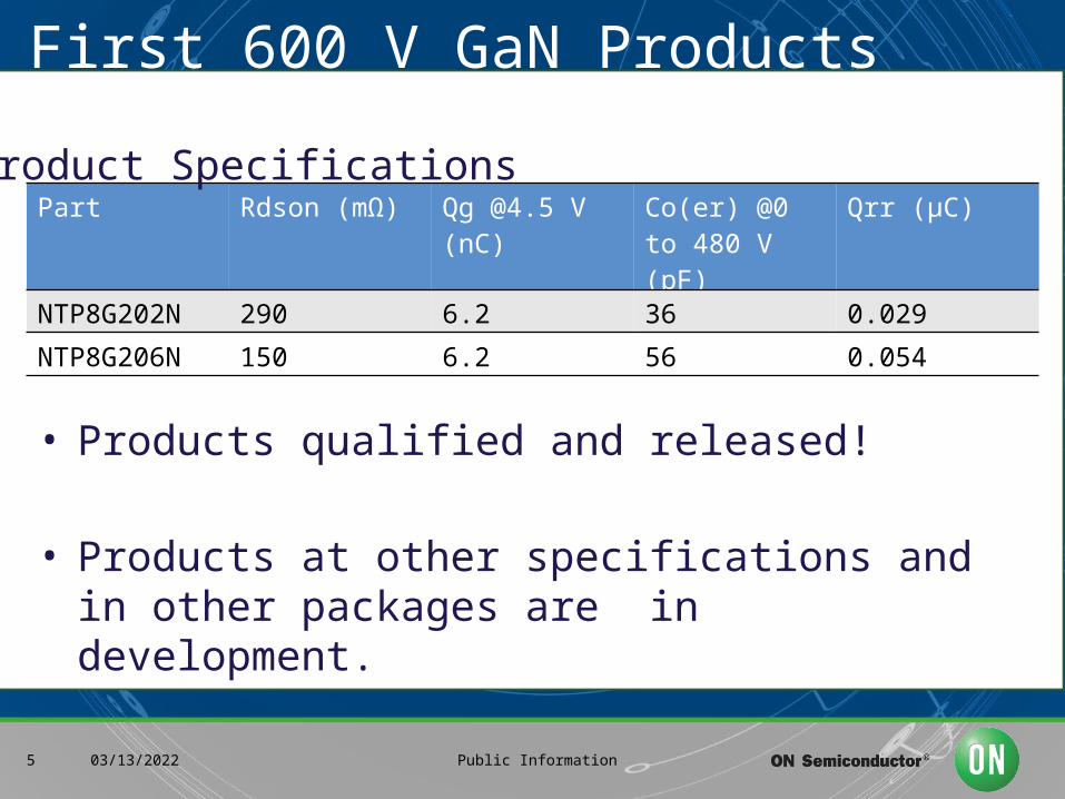
E
Part Rdson (mΩ) Qg @4.5 V (nC)
Co(er) @0 to 480 V (pF)
Qrr (µC)
NTP8G202N 290 6.2 36 0.029
NTP8G206N 150 6.2 56 0.054
First 600 V GaN Products
• Products qualified and released!
• Products at other specifications and in other packages are in development.
Product Specifications
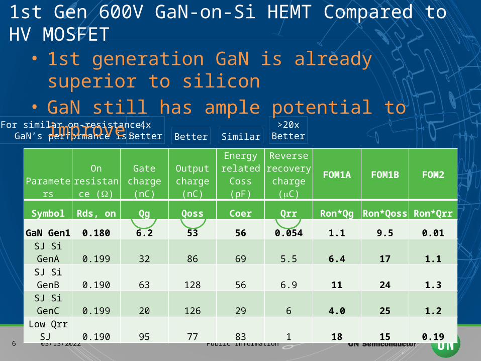
Public Information6 04/15/2023
Parameters
On resistance
(W)Gate charge
(nC)Output
charge (nC)
Energy related Coss
(pF)
Reverse recovery
charge (mC)FOM1A FOM1B FOM2
Symbol Rds, on Qg Qoss Coer Qrr Ron*Qg Ron*Qoss Ron*Qrr
GaN Gen1 0.180 6.2 53 56 0.054 1.1 9.5 0.01
SJ Si GenA 0.199 32 86 69 5.5 6.4 17 1.1
SJ Si GenB 0.190 63 128 56 6.9 11 24 1.3
SJ Si GenC 0.199 20 126 29 6 4.0 25 1.2
Low Qrr SJ 0.190 95 77 83 1 18 15 0.19
1st Gen 600V GaN-on-Si HEMT Compared to HV MOSFET
4xBetter Better Similar
>20xBetter
For similar on-resistance,GaN’s performance is:
• 1st generation GaN is already superior to silicon
• GaN still has ample potential to improve

Public Information7 04/15/2023
• Efficient power conversion favors soft switching circuit topologies that recover energy.– Phase-Shifted Full-Bridge– Half-Bridge or FB LLC– Synchronous Boost– Others
• GaN offers perfectly suited performance to accelerate this trend.
GaN ApplicationsIdeal Fit for Efficient Circuit Topologies

Public Information8 04/15/2023
• Drive and power loop inductances - Minimize component spacing
• Surge protection devices must be used• Ensure thermal performance by
appropriate heat sinking• Parallelization can be done by matching
gate drive and power loop impedances• Separate grounds for power and signal
components, connected at a single point
System Development for GaNCritical Factors
Public Information9 04/15/2023
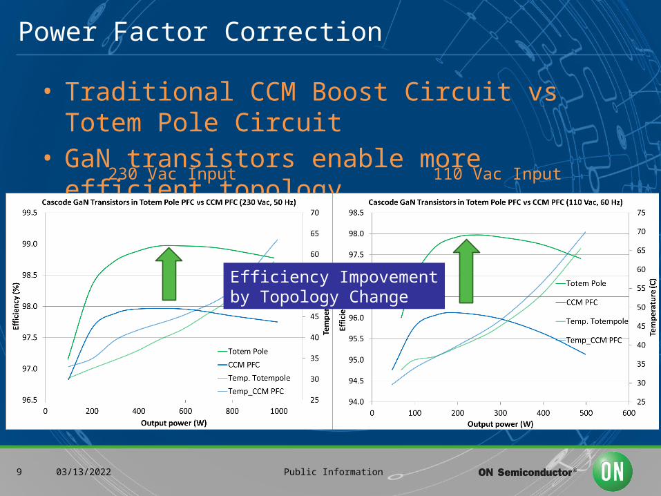
• Traditional CCM Boost Circuit vs Totem Pole Circuit
• GaN transistors enable more efficient topology
Power Factor Correction
230 Vac Input 110 Vac Input
Efficiency Impovementby Topology Change

Public Information10 04/15/2023
• Benefits from GaN at higher frequency – Increased power density– Reduced system size and weight
• System cost parity with better performance
• Component cost will reduce with volume to become lowest cost wide band gap technology
Advantages of GaN
Public Information11 04/15/2023
• GaN Transistors – ON Semiconductor and Transphorm collaborating to enable adoption in power systems
• Packaging – Advanced packaging technology to combine with characteristics of more ideal switches
• Drivers – High voltage drivers now, more coming for GaN
• Controllers – Applying strong market presence to GaN
• Reference Designs – Applying system expertise to GaN solutions for customers, not just products
Expertise in GaN Power Electronics...Poised to provide customers a TOTAL GaN solution.


