6-1 OVERVIEW Memory and data storage take many forms, even in a single computer system. Figure 6-1 classi- fies the various memory categories that are discussed in the following pages. There are two main classifications of memory families. These are RAM (Random Access Memory) and ROM (Read Only Memory) devices. RAM devices are volatile, which is to say they lose their memory content when the power to the host system is turned off. ROM devices are non-volatile, meaning they retain their stored data when the power is removed. RAM products are read and written to with the same electrical characteristics. They are easy to write but are volatile, meaning that when the power is turned off, the devices lose the memory content. ROM-based devices—ROM, EPROM, EEPROM, and flash memory devices are easy to read but are more difficult to program (write) than RAM devices. EEPROM and flash devices are more dif- ficult to program than they are to read. EPROMs need a mechanical step (UV-light) to erase the memory cells prior to re-programming the device. One-time programmable (OTP) EPROMs can INTEGRATED CIRCUIT ENGINEERING CORPORATION 6 GENERAL MEMORY TECHNOLOGY TRENDS Memories RAM Volatile Non Volatile Non Programmable One-Time Programmable Programmable Several Times ROM SRAM DRAM NVRAM BRAM FRAM EPROM EEPROM Flash ROM OTP 19993A Source: ICE, "Memory 1997" Figure 6-1. Memory Classification
Transcript
6-1
OVERVIEW
Memory and data storage take many forms, even in a single computer system. Figure 6-1 classi-fies the various memory categories that are discussed in the following pages. There are two mainclassifications of memory families. These are RAM (Random Access Memory) and ROM (ReadOnly Memory) devices. RAM devices are volatile, which is to say they lose their memory contentwhen the power to the host system is turned off. ROM devices are non-volatile, meaning theyretain their stored data when the power is removed.
RAM products are read and written to with the same electrical characteristics. They are easy to writebut are volatile, meaning that when the power is turned off, the devices lose the memory content.
ROM-based devices—ROM, EPROM, EEPROM, and flash memory devices are easy to read butare more difficult to program (write) than RAM devices. EEPROM and flash devices are more dif-ficult to program than they are to read. EPROMs need a mechanical step (UV-light) to erase thememory cells prior to re-programming the device. One-time programmable (OTP) EPROMs can
INTEGRATED CIRCUIT ENGINEERING CORPORATION
6 GENERAL MEMORY TECHNOLOGY TRENDS
Memories
RAM
Volatile Non VolatileNon
ProgrammableOne-Time
ProgrammableProgrammableSeveral Times
ROM
SRAM DRAM NVRAM BRAM FRAM EPROM EEPROM FlashROM OTP19993ASource: ICE, "Memory 1997"
Figure 6-1. Memory Classification
be written only one time by the user. ROM products are programmed during process manufac-turing. Figure 6-2 shows the different types of memories and some of the main characteristics ofthe devices.
GENERAL TECHNOLOGY ISSUES
Memory devices have historically been considered “process drivers” as well as revenue produc-ers. A process driver is a product that is manufactured in large wafer volumes, that pushes thestate-of-the-art in processing, and has a die yield that can be used to measure the effectiveness ofthe process.
General Memory Technology Trends
INTEGRATED CIRCUIT ENGINEERING CORPORATION6-2
FRAMDRAM SRAM ROMEPROM NVRAMFlashParallel
EEPROMCharacteristic
Cell Organization
Storage Method
Number of Devicesin Cell
Relative Cell Size
Density
Overhead Cost
Volatile (Power Off)
Data Retention(D.C. Power On)
In SystemReprogrammable
Number of ReprogramTimes (Endurance)
Typical Write(Reprogram) Speed
Typical ReadSpeed (ns)
1T + 1C
Charge onCapacitor
1.5
1.5
64Mbit
RefreshLogic
Yes
4ms
Yes
∞
100ns
100
1 Flip-Flop + 2T
Flip-flopcircuit
4-6
4-6
4Mbit
No
Yes
∞
Yes
∞
25ns
25
1T withFloating Gate
Charge onFloating Gate
1.0
1.5
16Mbit
UV EraseProgrammer
No
10 Years
No
100
30min
100
1T
Masked inProduction
1.0
1.0
64Mbit
MaskCharges
No
∞
No
—
—
100
1T + 1Twith Floating
Gate
Charge onFloating
Gate
2.0
3-4
4Mbit
No
No
10 Years
Yes
1,000,000
2.5s
200
1 SRAM Cell +1 EEPROM Cell
SRAM + Back-Upin EEPROM
8-9
9-10
256K
No
No
10 years
Yes
1,000,000
—
200
1T withFloating Gate
Charge onFloating Gate
1.0
1.5
64Mbit
No
No
10 Years
Yes
10,000
2.5s
200
1T + 1C
Charge onCapacitor
2.0
2.0
256K
No
No
10 Years
Yes
1012
235ns
150
Source: ICE, "Memory 1997" 22610
Figure 6-2. Characteristics of MOS Memory Product Types
Memories are no longer considered the only “process drivers” in the industry. That distinction isshared among memory, MPU, and ASIC devices. Intel, in the mid-1980s, made a strategic deci-sion to abandon the memory market for economic reasons. Intel probably had a good notion thatit could apply state-of-the-art processing techniques to microprocessors, thus making thesedevices process drivers as well.
Feature Size
The most critical issue in the advancement of IC technology is feature size; more specifically, theprogression to reduced feature sizes every few years. Today’s processes require considerableprocess adjustment with each feature size reduction. In addition, each new generation of memoryusually requires one or two additional mask layers. Figure 6-3 shows the past and projected fea-ture sizes for DRAMs and several other experimental devices. Design rules used to build thesedevices has decreased from about 3.0µm in 1980 to about 0.25µm in 1997. This represents about a14 percent decrease every year. This trend is expected to continue and feature sizes are forecast tobe about 0.15µm by 2000.
Figure 6-4 shows SIA’s technology roadmap through the year 2010. As shown, the integrationlevels are forecast to continue along historical trend lines.
1990 Forecasted CommercialLimit For Optical Lithography (0.35µ)
= Laboratory Reasearch
MIT (0.06µ)X-Ray
Bell Labs(0.14µ)
Toshiba(0.25µ) IBM
(0.25µ)Gate Array
(X-Ray)
Loose Production ResolutionTight Production Resolution
Development
HMOS II(2.0µ)
HMOS IV(1.0µ) 4M DRAM
(0.8µ)16M DRAM
(0.5µ)64M DRAM
(0.35µ)
256K DRAM(1.6µ) 1M DRAM
(1.2µ)
16M DRAM(0.5µ)
64M DRAM(0.35µ)
4M DRAM(0.8µ)
WE 3210032-Bit MPU
(1.5µ)
10981RSource: ICE, "Memory 1997"
95
256MDRAM(0.25µ)
256MDRAM(0.25µ)
1992 Forecasted CommercialLimit For Optical Lithography (0.15µ)
97
1G DRAM(0.15µ)
Toshiba(0.1µ)
Toshiba(0.04µ)
98 0200
(2.0µ)
(1.0µ)
(0.7µ)
4GDRAM(0.08µ)
1GDRAM(0.15µ)
1996 Forecasted CommercialLimit for Optical Lithography (0.1µ)
Figure 6-3. IC Feature Size Trends
Lifecycle
As with any commercial product, memories have a lifecycle. A memory will pass through the dif-ferent steps of the lifecycle, from its introduction where the IC manufacturer concentrates on cap-ital resources and R&D efforts, to the end of its life when the product becomes obsolete.
General Memory Technology Trends
INTEGRATED CIRCUIT ENGINEERING CORPORATION6-4
Year of first DRAM shipment
Minimum feature (µm)
Memory DensityBits/chip (DRAM/flash)
Logic Density (High volume: Microprocessor)Logic transistors/cm2 (packed)Bits/cm2 (cache SRAM)
Logic Density (Low volume: ASIC)Transistors/cm2 (auto layout)
Number of Chip I/OsChip to package (pads) high performance
Chip frequency (MHz)On-chip clock, cost-performanceOn-chip clock, high-performanceChip-to-board speed, high performance
Chip size (mm2)DRAMMicroprocessorASIC
Oxide Thickness (nm)
Junction Depth (µm)
Maximum number wiring levels (logic)On-chip
Minimum mask count
Power supply voltage (V)DesktopBattery
Maximum powerHigh performance with heatsink (W)Logic without heatsink (W/cm2)Battery
1995
0.35
64M
4M2M
2M
900
150300150
190250450
7-12
0.1-0.2
4–5
18
3.32.5
805
2.5
1998
0.25
256M
7M6M
4M
1,350
200450200
280300660
4-6
0.1-0.15
5
20
2.51.8–2.5
1007
2.5
2001
0.18
1G
13M20M
7M
2,000
300600250
420360750
4-5
0.07-0.13
5–6
20
1.80.9–1.8
120103.0
2004
0.13
4G
25M50M
12M
2,600
400800300
640430900
4-5
0.05-0.1
6
22
1.50.9
140103.5
2007
0.10
16G
50M100M
25M
3,600
5001,000375
960520
1,100
<4
<0.07
6–7
22
1.20.9
160104.0
2010
0.07
64G
90M300M
40M
4,800
6251,100475
1,400620
1,400
<4
<0.05
7–8
24
0.90.9
180104.5
Driver
D
L(µP)
L(A)
L,A
µP
L
µP
µP
µP
L
µPA
µPAL
A=ASICL=Logic
D=DRAMµP=Microprocessor
20286CSource: SIA/ICE, "Memory 1997"
Figure 6-4. The 15-Year SIA Roadmap
Die Size Trends
In 1975, Intel Chairman Gordon Moore predicted that engineers could shrink semiconductordevice dimensions by approximately 10 percent each year, creating a new generation of chipsevery three years with four times as many transistors. Twenty one years later, Moore’s predictionwas impressively accurate. DRAM devices actually exceeded his expectations (Figure 6-5).
Figure 6-6 shows how the die area of leading-edge memory devices has increased about 13 per-cent per year. The trend toward larger die sizes is forecast to continue. The die sizes of the 1GbitDRAMs described at the 1995 and 1996 ISSCC conferences ranged from 901K sq. mils to 1,451K sq.mils (Figure 6-7). As shown, the NEC 1Gbit DRAM, if square, would be about 1.2 inches on a side.
Wafer Size
The IC industry is quickly moving to the new 300mm (12 inch) wafer standard. Figure 6-8 showsthe wafer area increase that occurs each time the industry moves to the next wafer size. Currentlythe standard for high-volume advanced IC production is 200mm (8 inch). The area gained bymoving from 200mm to 300mm wafers will be 125 percent.
Advancing from one wafer size to a new, larger size takes several years of development. In fact,development time increased substantially to transition to 200mm wafers and will be the same forthe transition to 300mm wafers (Figure 6-9). Companies such as Samsung, Texas Instruments, andmany other leading memory suppliers have indicated their willingness to build manufacturingfacilities to support 300mm wafers. The big question is which company will be the one to take onthe huge headaches and huge amount of capital needed to work out all the wrinkles associatedwith the transition to 300mm wafers.
1 Produced using KrF excimer-laser lithography.2 Packaged in a 64-pin 600-mil TSOP, produced using e-beam lithography.3 SDRAM produced using synchrotron-generated x-ray lithography.4 SDRAM produced using KrF excimer-laser lithography.
20289ASource: ICE, "Memory 1997"
Figure 6-7. ISSCC Advanced DRAMs
Defect Density
The cost to manufacture ICs is governed by many factors. One of the most important is thenumber of good dice per wafer started into the wafer fab. This number is dependent on thenumber of potential dice per wafer, and the number of defective dice.
Figure 6-9. Wafer Development Time Requirements (Time to Reach 100 MSI Production Rate)
Figure 6-10 shows the potential number of dice for various wafer sizes. The number of potentiallygood dice per wafer is dependent on the wafer size and the die size. The number of defective diceon a wafer are the result of random killer defects, usually expressed in defects per square cen-timeter, and the number of defective dice caused by parametric defects. In a world class fab, thenumber of dice lost because of parametric defects is very low.
As shown in Figure 6-11, random killer defects have a dramatic effect on the number of good diceper wafer, especially as the die size increases. Figure 6-12 shows the yield effect of various defectdensities versus die size, where the yield is defined as the number of good dice divided by thenumber of potential dice.
Defect density control is extremely important for memory fabs since the cell array area in a memoryIC contains extremely compact circuitry. Each generation (256Kbit, 1Mbit, 4Mbit, etc.) of memorychip is about 50 percent larger than the previous with four times the number of bits of storage.
As feature sizes become smaller, ICs are susceptible to smaller and smaller particles causingrandom killer defects. This means that if everything else remains constant, the killer defect den-sity will increase as smaller particulates become killer defects. Yield also decreases with increas-ing die sizes. Therefore, to maintain acceptable yields, extreme care must be taken to reduceparticulates in the ambient air, the equipment, the process gases, and the process liquids.
Fab processes themselves generate particulates that can cause defects. In modern processes, eachprocess step is given a defect “budget” for the number of defects per square centimeter added forthe step. As the number of process steps increases, the job of reducing the defect density becomesmore and more difficult.
Redundancy
As mentioned earlier, the effect of defect density on memory chips is a much larger problem thanwith most other products due to the circuit density in the storage cell array. Nearly any particu-late-caused defect in this area is a killer defect. To enhance memory chip yields, manufacturersuse spare rows and columns (redundant rows and columns) that can replace defective rows orcolumns. During 100 percent wafer probe, defective rows and columns are “replaced” by thesespares through the use of laser blown fuses that alter the decode mechanism. When external sig-nals try to access a defective row or column, the decode circuitry selects a spare one instead.Figure 6-13 shows a simplified logic of redundancy programming. A normal decoder containshalf as many decoding transistors as a redundant decoder. If redundancy is not required—that is,the chip is perfect—spare decoders will be deselected regardless of the input address.
Figure 6-12. Murphy’s Probe Yield Model (As a Function of Defects per sq cm)
Process Complexity
Process complexity is usually measured by the number of critical mask layers, plus any specialprocesses that may have a detrimental effect on yield. As feature sizes have become smaller, struc-tures under the surface of the silicon wafer have become more shallow. The structures above thewafer surface have remained relatively thick. The thicker interconnect layers are the result of theneed to separate the conductive layers as much as possible, thus reducing the capacitive loadingof the long thin conductors (polysilicon and aluminum) running the length and width of the chip.If the deposited dielectric films are reduced in thickness, the parasitic capacitive load will increase,and the device will be considerably slower.
Several manufacturers have lowered the effect of parasitic capacitance through the use of materi-als with lower dielectric constants. Polyimide is one such material. The dielectric constant ofpolyimide is below 3.0, versus 3.9 for deposited silicon dioxide. The improvement in reduced par-asitic capacitance is a linear function with respect to dielectric constant.
General Memory Technology Trends
INTEGRATED CIRCUIT ENGINEERING CORPORATION 6-11
VDDVDD
ChipEnable,
CE
A , Ao o A , An n
LaserProgrammable
Link
VDD
VDD
Ao Ao An An
CE
SPARE DECODER
17612Source: ICE, "Memory 1997"
Figure 6-13. Row Decode for Redundancy
Although the number varies somewhat from vendor to vendor, over twenty critical mask steps arerequired to produce today’s most advanced memory chips. Each new generation requires one ortwo additional mask layers. Each mask layer is composed of ten to twenty actual process opera-tions, some major and some minor.
With today’s processes composed of hundreds of steps, the requirement for tight process controlon each step is critical. When processes are planned, budgets are established for process varia-tions at each process step. These budgets are modeled and used to predict manufacturability.Uniformity across the die, across the wafer, from wafer to wafer, and from wafer lot to wafer lotcan be predicted.
The size of memory chips is obviously very dependent on the size of a single memory cell.Reducing the feature size reduces the cell (storage area for one bit) somewhat, but there are por-tions of the cell that do not reduce with feature size. To continue the reduction of cell area, designsare now utilizing three-dimensional structures. These will be described later in the various prod-uct descriptions, but in all cases, the addition of these structures leads to additional process steps.
POWER SUPPLY
Two factors are driving the reduction in memory operating voltages: power dissipation andprocess geometries. The market for low-voltage devices is growing fast, and IC manufacturers areconcentrating significant R&D efforts to develop low-voltage versions of their memory ICs.
Power Dissipation
The demand for low power dissipation comes from two main factors. First, system and packagepower constraints demand lower operating voltage due to higher board integration and the useof more integrated chips.
Systems with dual power supplies (5V and 3.3V) consume system space and require careful inter-face design between the two supplies. For this reason, system manufacturers push ICs suppliersto produce low voltage devices so that they can design single low-voltage supply systems. Figure6-14 shows the market transition from 5V to 3V systems.
The second reason for the rise in low-power ICs comes from growth in the portable electronicsmarket including portable computers and digital cellular phones. This equipment requires lowpower and low voltage to increase battery life. Dissipation drops 36 percent when going from5.5V to 3.3V, for example. Using 2.7V in a typical digital cellular phone design could extend talktime by 25 percent over 3.3V operation. Figure 6-15 shows 5V to 3.3V power savings in a typicalnotebook computer.
General Memory Technology Trends
INTEGRATED CIRCUIT ENGINEERING CORPORATION6-12
An extra incentive for designing 3.3V ICs is the U.S. government’s EPA Energy Star Program.According to the EPA, computer systems account for five percent of commercial electricity con-sumption in the United States. Energy Star mandated energy reduction in any PC the federal gov-ernment purchased.
*Hard-disk drive power estimates reflect a mix of active and idle time.Source: Cirrus Logic/Electronic Products/ICE, "Memory 1997" 19217
Figure 6-15. 3.3V Logic Power Savings in a Typical Notebook Computer
Process Geometries
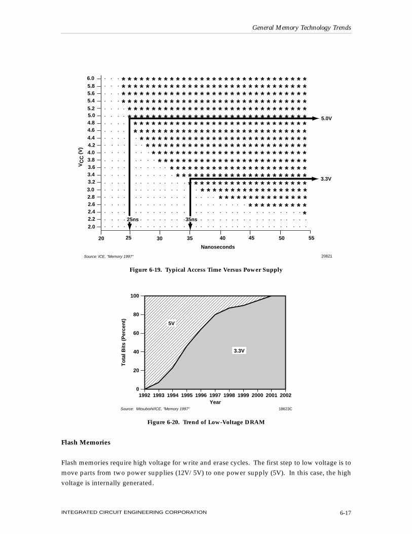
For memory devices to become increasingly dense, feature sizes must shrink. Both gate oxidesand gate lengths need lower voltage to avoid an increase in electrical field (Figures 6-16 and 6-17).For a similar process on a given generation, 3.3V parts have longer access times than 5V parts.Figure 6-18 gives the supply voltage decrease versus the technology and the memory density.
Unfortunately, it is more difficult to yield high-speed devices for low voltage ICs than it is forhigh voltage parts. Figure 6-19 shows a typical schmoo plot of the access time versus powersupply.
DRAMs
During 1994, there was a significant ramping-up of low-voltage DRAMs (Figure 6-20). ICE fore-casts that in the year 2002, more than 95 percent of all DRAMs sold will be classified as low-volt-age (3.3V or lower).
Some PC manufacturers have delayed shifting to pure 3.3V motherboard designs because pricepremiums for 3.3V DRAMs would negatively impact the cost of their system. However, during1996, all major DRAM suppliers were making the transition to 3.3V at the 16Mbit DRAM level.
General Memory Technology Trends
INTEGRATED CIRCUIT ENGINEERING CORPORATION6-14
160
140
120
100
80
60
40
20
0
0 0.1 0.2 0.3 0.4 0.5 0.6
Gate Length (µm)
Gat
e O
xid
e T
hic
knes
s (Å
)
Published Data
Trend Line
20284ASource: Intel/ICE, "Memory 1997"
Figure 6-16. Gate Oxide Versus Gate Length
Price parity between 5V and 3.3V devices should quickly ensue. 64Mbit DRAMs are proposedonly at the 3.3V level. The upcoming 256Mbit DRAM will operate internally at around 2.5V butwill interface to 3.3V.
Certain drawbacks exist for DRAMs operating at lower internal voltages. For instance, it is moredifficult to read the charge on a cell capacitor when a lower voltage is stored on the capacitor. Thecell is also more susceptible to errors due to ground bounce (electrical noise) caused by the simul-taneous reading of several hundred cells at one time.
SRAMs
Advanced SRAMs are shifting to 3.3V technology even though there is a speed penalty versus acomparable 5V part. In terms of data sensitivity (i.e., noise immunity, alpha particles), the 6TCMOS cell is the best design. The benefits of a TFT (Thin Film Transistor) cell are described inSection 8. One additional benefit of the TFT is reduced power consumption. However, due toprocess complexity, most SRAM manufacturers stay away from this design.
ROMs
ROM technology is not necessarily state-of-the-art, but these products are moving to lower volt-age operation like the other memory technologies. Several manufacturers have proposed low-voltage ROMs. Sharp offers 16Mbit and 32Mbit ROMs with power supplies ranging from 2.7V to3.6V. Other ROM makers such as AMI, Hitachi, and Ricoh also offer low-voltage ROMs.
General Memory Technology Trends
INTEGRATED CIRCUIT ENGINEERING CORPORATION 6-15
6
5
4
3
2
1
00 0.1 0.2 0.3 0.4 0.5 0.6
Published Data
Trend Line
Op
erat
ing
Vo
ltag
e (V
)
Gate Length (µm)
20285ASource: Intel/ICE, "Memory 1997"
Figure 6-17. Gate Length Versus Operating Voltage
EPROMs
The development of high-density EPROMs has slowed due to the evolution of flash memories.However, like other technologies, low-voltage parts are available. The low-voltage supply is onlyused for read operations. High voltages are required for the write operations (Figure 6-21).
EEPROMs
EEPROMs must internally generate high voltage for write/erase operations. The VCC powersupply affects the internal high voltage supply (VPP). Low-voltage parts are much more complex.There is, however, a need for low-power parts in applications such as digital cellular phones. 2.7Vto 3.6V power supply EEPROM devices are available from several vendors.
General Memory Technology Trends
INTEGRATED CIRCUIT ENGINEERING CORPORATION6-16
1K 4K 16K 64K 256K 1M 4M 16M 64M 256M
1M/4M 16M 32M 64M 256M
1G
10
1
0.1
12V
5V
3.3V
1.5V
1970 1980 1990 2000
Pro
cess
Tec
hn
olo
gy
Year
Su
pp
ly V
olt
age
8µm
5µm3µm
2µm
1.3µm
0.8µm
0.5µm0.35µm
0.25µm
0.15µm
Source: Hitachi, "Memory 1997" 20872A
256 1K 4K 16K 64K 256K 1M 4M 4M 16M 64M
DRAM
SDRAM
FLASH1992/1993 1994 1995 1996 1999
Figure 6-18. Technology Roadmap/Wafer Process
Flash Memories
Flash memories require high voltage for write and erase cycles. The first step to low voltage is tomove parts from two power supplies (12V/5V) to one power supply (5V). In this case, the highvoltage is internally generated.
AMD has emphasized its low-voltage, single-voltage flash products. AMD introduced an 8Mbitflash device at 3.0V only (but with a range from 2.7V to 3.6V). The part has the 2.7V to 3.6V volt-age range for both read and write operations.
Intel promotes its Smart 3 family belonging to the SmartVoltage concept that allows voltage flex-ibility. The memory can be read and written at multiple voltages. The Smart3 family includes4Mbit, 8Mbit, and 16Mbit devices with 2.7V-3.6V for read operation and program/erase plus 12Vfor fast programming capability.
Unified Memory Architecture (UMA)
The Video Electronics Standard Association (VESA) proposed a new architecture for PCs calledUnified Memory Architecture (UMA). The goal of this architecture is to lower the price of the PCsby eliminating some memory.
In the traditional PC memory architecture, a frame-buffer memory is used for the graphics subsys-tem and a DRAM array is used as main memory. The new PC bus configuration proposal suggeststhat both main memory and the graphics frame-buffer use a common DRAM array. A graphicsframe-buffer uses 1 to 2Mbytes of memory. This would be included in the main DRAM array. Byeliminating the separate frame-buffer memory chip in the PC, a cost savings of between $30 and$80 could be realized.
The UMA design, however, reduces the performance of the PC. Speed degradation is estimatedat anywhere between 5 and 20 percent. For this reason, UMA targets the low-end applicationswhere price is more important than performance. Figure 6-22 shows the traditional architectureversus the VESA UMA architecture. Companies that have developed chip sets for UMA basedsystems are shown in Figure 6-23.
Among the difficulties UMA faces is lack of support from some major companies. For example,Microsoft says that the performance of an 8Mbyte UMA system using Windows 95 is decreasedtoo much, as available memory is reduced by 1Mbyte.
General Memory Technology Trends
INTEGRATED CIRCUIT ENGINEERING CORPORATION6-18
Vcc (Read Mode)
Vpp (Read Mode)
Vcc (Write Mode)
Vpp (Write Mode)
3.3V
Vcc
6.5V
13V
19964Source: ICE, "Memory 1997"
Figure 6-21. Low-Voltage EPROM
Intel, also, does not support UMA. In fact, it developed another architecture called SharedMemory Buffer Architecture (SMBA). SMBA minimizes the impact on processor performancefrom sharing partitioned system memory with the graphics controller by using smart-bufferingprogrammable timers with a strict latency policy.
Latch-up
A major limitation to bulk CMOS technology is the inherent parasitic bipolar transistors that occuras a natural part of the CMOS structures. The CMOS structure forms parasitic bipolar PNP andNPN transistors that are the electrical equivalent of a silicon controlled rectifier (SCR). The para-sitic device is electrically connected across the VDD and VSS power supply and input or output
General Memory Technology Trends
INTEGRATED CIRCUIT ENGINEERING CORPORATION 6-19
Processor
Chip Set
DRAM WithFrame Buffer
GUIAccelerator
PCI OrISA Bus
Video Out
VESA UMA
Source: ICE, "Memory 1997" 20871
GUIAccelerator
FrameBuffer
TRADITIONAL ARCHITECTURE
Processor
Chip Set
Video Out
DRAM
Figure 6-22. Traditional Memory Architecture Versus Unified Memory Architecture
Vendor
Acer Labs
Cirrus Logic
Opti
S3
Trident Micro
Via Technology
VLSI Technology
Model
Aladdin lll
CL-GD54UM36
Viper-UMA
Trio 64UV+
TGUl9682
Apollo VP-1
In Development
TargetSystems
Pentium
Pentium
Pentium
Low-end Pentium
Pentium
Pentium
P54C, P6, Power PC
ClockRate (MHz)
75-100
75-100
75-100
75-100
75-100
75-100
100 and up
IntelSMBA
No
No
No
Yes
Yes
No
No
VESA-UMA
Yes
Yes
Yes
Yes
Yes
Yes
Yes
Remarks
—
Graphs Accelerator
—
—
Graphics Accelerator
—
—
20873ASource: Electronic Business Today, "Memory 1997"
Figure 6-23. Comparing UMA Products
pads. Thus, if this parasitic device conducts, it establishes a very low resistance path to the powersupply and can cause very large amounts of current to flow through the structure. This phenom-enon is shown in Figure 6-24. Since there are many PNPN devices on a CMOS chip, it is possibleto trigger any one device into conduction and cause the latch-up problem.
The phenomenon of latch-up is well understood by memory designers and many approacheshave been taken to eliminate it. However, the latch-up sensitivity of a CMOS circuit increases inseverity as device dimensions continue to shrink. Therefore, new latch-up reduction techniqueswill be needed in the future as the process geometries become smaller.
Conditions that trigger latch-up can come from several different places in an electronic systemincluding over-voltage stress, voltage transients, radiation-induced photocurrents, or the inputprotection circuit being over driven.
Some of the methods used to control latch-up include guard rings, epitaxy on a heavy doped sub-strate, epitaxy/buried layer CMOS structures, Schottky clamps, physical barriers to lateral cur-rents, trench isolation, total dielectric isolation, and well controlled design rules.
General Memory Technology Trends
INTEGRATED CIRCUIT ENGINEERING CORPORATION6-20
A A AAnode
B B BCathode
p
n
p
p
n
p
n
n
p
n
VDDVoltage
Cu
rren
t
IH
b) I-V characteristicsa) transistor equivalent circuit16660BSource: ICE, "Memory 1997
The Four Layer Diode
���� ����������������
������������
���������
������������
������������
������������
OxideVSS(–)(+)VDD
VIN
VOUT
G GD DS S
P+N+N+P+P+N+
P–P-WellCurrent
IRW
IRSSubstrateCurrent
n-substrate
Figure 6-24. Bulk CMOS Inverter With pnpn Latch-Up Path
The Electronic Industries Association (EIA) under the direction of a JEDEC committee publishedJEDEC standard no. 17, “Latch-Up in CMOS Integrated Circuits.” This is a standard used for test-ing CMOS circuits for latch-up problems.