73
George Mason University ECE 448 – FPGA and ASIC Design with VHDL FPGA Platforms High Level Language (HLL) Design Flows ECE 448 Lecture 21
| Date post: | 19-Dec-2015 |
| Category: |
Documents |
| Upload: | tamsin-banks |
| View: | 233 times |
| Download: | 3 times |

George Mason UniversityECE 448 – FPGA and ASIC Design with VHDL
FPGA Platforms
High Level Language (HLL)Design Flows
ECE 448Lecture 21
2ECE 448 – FPGA and ASIC Design with VHDL
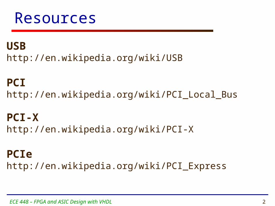
Resources
USBhttp://en.wikipedia.org/wiki/USB
PCIhttp://en.wikipedia.org/wiki/PCI_Local_Bus
PCI-Xhttp://en.wikipedia.org/wiki/PCI-X
PCIehttp://en.wikipedia.org/wiki/PCI_Express

3ECE 448 – FPGA and ASIC Design with VHDL
Resources
• Clive „Max” Maxfield, The Design Warrior’s Guide
to FPGAs
Chapter 11 C/C++ etc.-Based Design Flows
Reconfigurable SupercomputingT. El-Ghazawi, K. Gaj, D. Buell, D. PointerTutorial at the Supercomputing 2005 conferencehttp://hpcl.seas.gwu.edu/openfpga/tutorial_html/index.html

4ECE 448 – FPGA and ASIC Design with VHDL
FPGA Device Capacity Trends
Year1985
Xil
inx
Dev
ice
Com
ple
xity
XC200050 MHz1K gates
XC4000100 MHz
250K gates
Virtex200 MHz1M gates
Virtex-II 450 MHz8M gates
Spartan80 MHz
40K gates
Spartan-II200 MHz
200K gates
Spartan-3326 MHz5M gates
19911987
XC300085 MHz
7.5K gates
Virtex-E240 MHz4M gates
XC520050 MHz
23K gates
1995 1998 1999 2000 2002 2003
Virtex-II Pro450 MHz8M gates*
2004 2006
Virtex-4500 MHz
16M gates*
Virtex-5550 MHz
24M gates*
Source: http://class.ece.iastate.edu/cpre583/lectures/Lect-01.ppt

5ECE 448 – FPGA and ASIC Design with VHDL
Prices of the most recent families of Xilinx FPGAs
Spartan 3 Virtex II, Virtex II-Pro
< $130* < $3,000*
Spartan 3E Virtex 4, Virtex 5
< $35* < $3,000*
* approximate cost of the largest device per unit for
a batch of 10,000 units
Low-cost High-performance
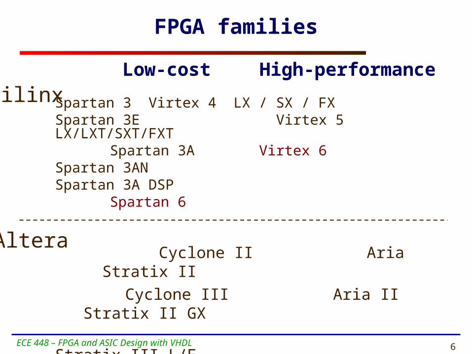
6ECE 448 – FPGA and ASIC Design with VHDL
FPGA families
Spartan 3 Virtex 4 LX / SX / FXSpartan 3E Virtex 5 LX/LXT/SXT/FXT
Spartan 3A Virtex 6Spartan 3ANSpartan 3A DSP
Spartan 6
Low-cost High-performance
Xilinx
Altera Cyclone II Aria Stratix II
Cyclone III Aria II Stratix II GX
Stratix III L/E
Stratix IV E/GX/GT
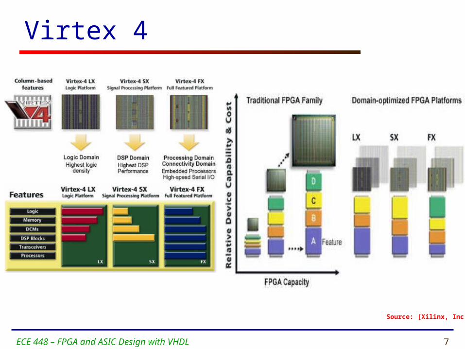
7ECE 448 – FPGA and ASIC Design with VHDL
Virtex 4
Source: [Xilinx, Inc.]
8ECE 448 – FPGA and ASIC Design with VHDL
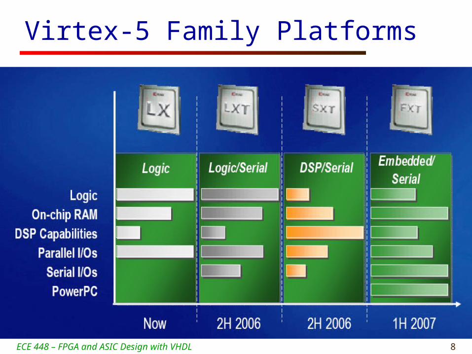
Virtex-5 Family Platforms

George Mason UniversityECE 448 – FPGA and ASIC Design with VHDL
FPGA Boards

10ECE 448 – FPGA and ASIC Design with VHDL
General Architecture of an FPGA-Based Board
BU
S
ProcessingElement(PE#0)
ProcessingElement(PE#1)
ProcessingElement(PE#N-1)
COMMON MEMORY / INTERCONNECT NETWORK
LOCALMEMORY
LOCALMEMORY
LOCALMEMORY
CLK
BUS INTERFACE CONTROLLER
I/O CARD
11ECE 448 – FPGA and ASIC Design with VHDL
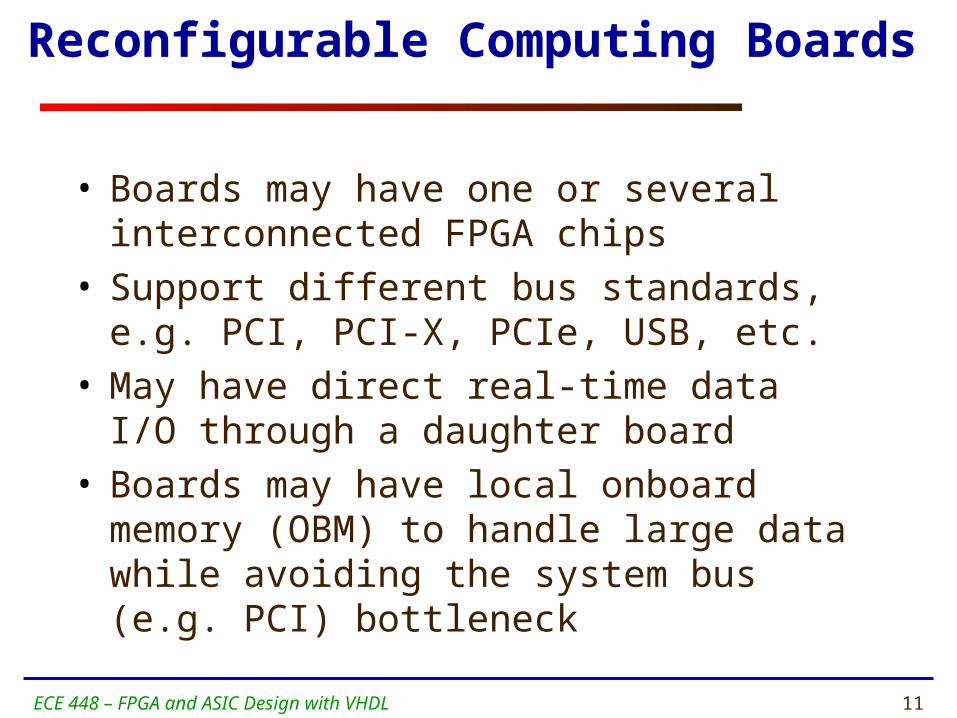
Reconfigurable Computing Boards
• Boards may have one or several interconnected FPGA chips
• Support different bus standards, e.g. PCI, PCI-X, PCIe, USB, etc.
• May have direct real-time data I/O through a daughter board
• Boards may have local onboard memory (OBM) to handle large data while avoiding the system bus (e.g. PCI) bottleneck

12ECE 448 – FPGA and ASIC Design with VHDL
• Many boards per node can be supported
• Host program (e.g. C) to interface user (and P) with a board via the board’s API
• Driver API functions may include functionalities such as Reset, Open, Close, Set Clocks, DMA, Read, Write, Download Configurations, Interrupt, Readback
Reconfigurable Computing Boards

13
Universal Serial Bus (USB)
It supports three data rates.
• Full speed rate of 1.5 MB/s as defined by USB 1.0.
• Low speed rate of 1.5 Mb/s which is also defined by USB 1.0. Very similar to full speed operation except that it takes each bit 8 times as long to transmit. Devices that run on the low speed rate are Keyboards, Mice and Joysticks.
• High speed rate of 60 MB/s as defined by USB 2.0.
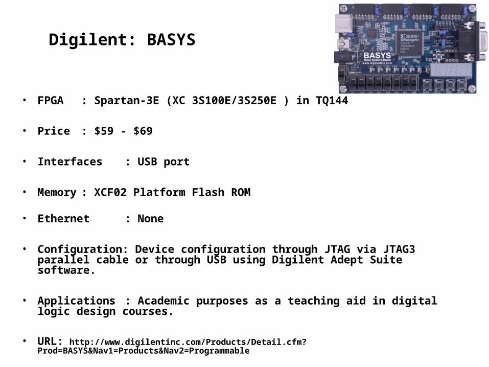
Digilent: BASYS
• FPGA : Spartan-3E (XC 3S100E/3S250E ) in TQ144
• Price : $59 - $69
• Interfaces : USB port
• Memory : XCF02 Platform Flash ROM • Ethernet : None
• Configuration: Device configuration through JTAG via JTAG3 parallel cable or through USB using Digilent Adept Suite software.
• Applications : Academic purposes as a teaching aid in digital logic design courses.
• URL: http://www.digilentinc.com/Products/Detail.cfm?Prod=BASYS&Nav1=Products&Nav2=Programmable

Digilent: Spartan3E starter board
• FPGA : Spartan-3E (XC3S500E)
• Price : $149
• Interfaces : USB3 port
• Memory : XCF04 Platform Flash for storing FPGA configurations, 16 Mb Serial Flash, 128 Mb Strata Flash, 256 Mb DDR SDRAM
• Ethernet : 10/100 Ethernet PHY
• Configuration: JTAG programming via on-board USB3 port; JTAG and SPI Flash programming with parallel or JTAG USB cable
• Applications : General Prototyping.
• URL: http://www.digilentinc.com/Products/Detail.cfm?Prod=S3EBOARD&Nav1=Products&Nav2=Programmable
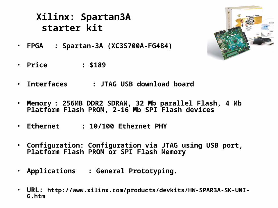
Xilinx: Spartan3A starter kit
• FPGA : Spartan-3A (XC3S700A-FG484)
• Price : $189
• Interfaces : JTAG USB download board
• Memory : 256MB DDR2 SDRAM, 32 Mb parallel Flash, 4 Mb Platform Flash PROM, 2-16 Mb SPI Flash devices
• Ethernet : 10/100 Ethernet PHY
• Configuration: Configuration via JTAG using USB port, Platform Flash PROM or SPI Flash Memory
• Applications : General Prototyping.
• URL: http://www.xilinx.com/products/devkits/HW-SPAR3A-SK-UNI-G.htm
17ECE 448 – FPGA and ASIC Design with VHDL
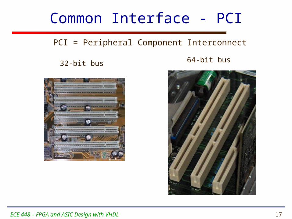
Common Interface - PCI
PCI = Peripheral Component Interconnect
32-bit bus 64-bit bus

18
Evolution of the PCI Interface
ECE 448 – FPGA and ASIC Design with VHDL
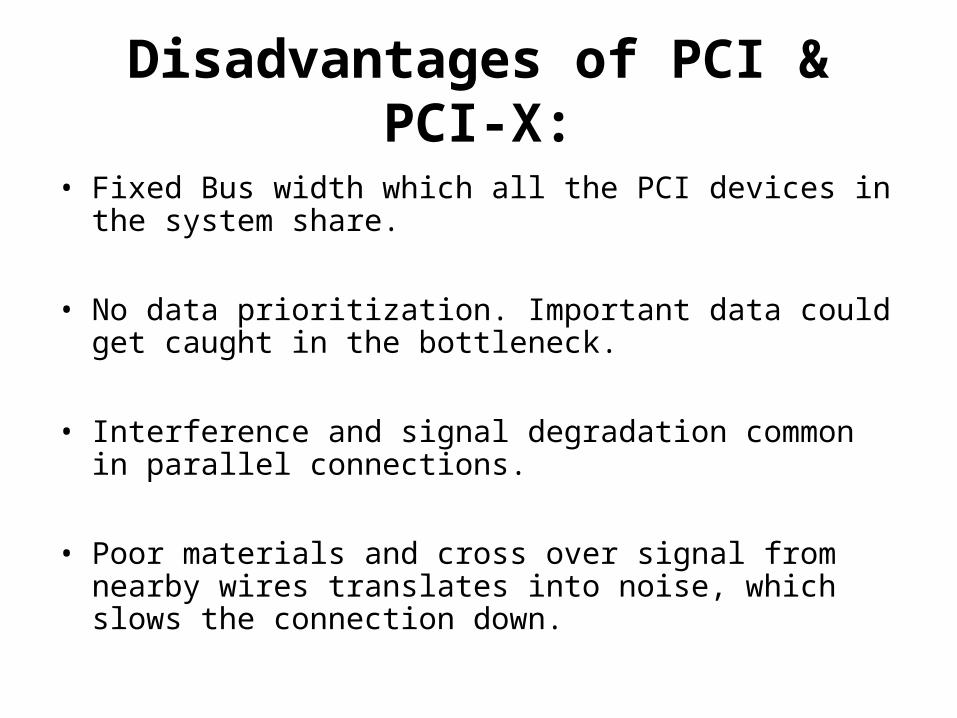
Disadvantages of PCI & PCI-X:
• Fixed Bus width which all the PCI devices in the system share.
• No data prioritization. Important data could get caught in the bottleneck.
• Interference and signal degradation common in parallel connections.
• Poor materials and cross over signal from nearby wires translates into noise, which slows the connection down.

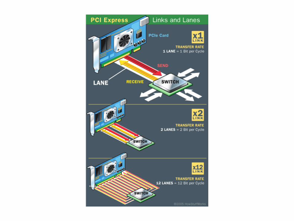
PCI Express (PCIe):
• Not a bus like PCI or PCI-X. Communication based on the concept of lanes.
• A serial bi-directional point-to-point connection is known as a lane.
• Full duplex bi-directional lanes.
• Transfer rate of a single Lane is a single bit/cycle in each direction.
• Different PCI lane configurations: x1, x2, x4, x8, x16, x32.
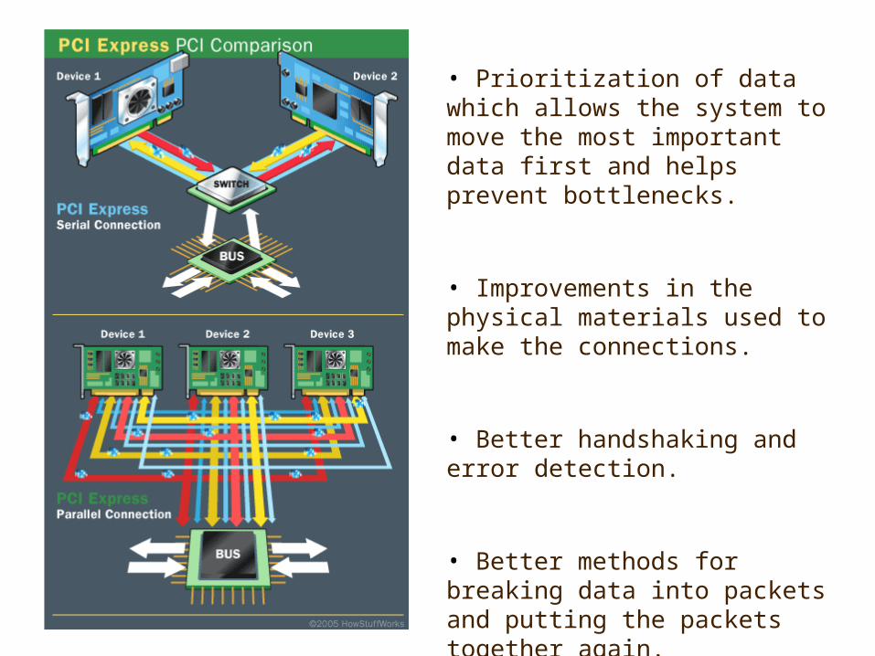
• Prioritization of data which allows the system to move the most important data first and helps prevent bottlenecks.
• Improvements in the physical materials used to make the connections.
• Better handshaking and error detection.
• Better methods for breaking data into packets and putting the packets together again.
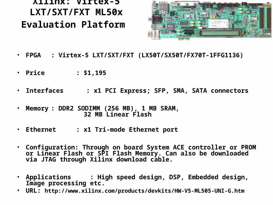
Xilinx: Virtex-5 LXT/SXT/FXT ML50x
Evaluation Platform
• FPGA : Virtex-5 LXT/SXT/FXT (LX50T/SX50T/FX70T-1FFG1136)
• Price : $1,195
• Interfaces : x1 PCI Express; SFP, SMA, SATA connectors
• Memory : DDR2 SODIMM (256 MB), 1 MB SRAM, 32 MB Linear Flash
• Ethernet : x1 Tri-mode Ethernet port
• Configuration: Through on board System ACE controller or PROM or Linear Flash or SPI Flash Memory. Can also be downloaded via JTAG through Xilinx download cable.
• Applications : High speed design, DSP, Embedded design, Image processing etc.
• URL: http://www.xilinx.com/products/devkits/HW-V5-ML505-UNI-G.htm

Xilinx: Virtex-5 FXT ML510 Embedded Development
Platform • FPGA : Virtex-5 FXT (XC5VFX130T-2FFG1738)
• Price : $3,100
• Interfaces : x2 PCIe downstream connectors,x4 32-bit @33 MHz PCI connectors; x2 SATA connectors
• Memory : 512 MB Compact Flash card, x2 72-bit DDR2 DIMMs (512 MB)
• Ethernet : x2 Tri-mode Ethernet ports
• Configuration: Through on board System ACE controller with the configuration files stored in the CF card.
• Applications : Embedded design, High speed design, Digital video, Telecom/Datacom etc.
• URL: http://www.xilinx.com/products/devkits/HW-V5-ML510-G.htm
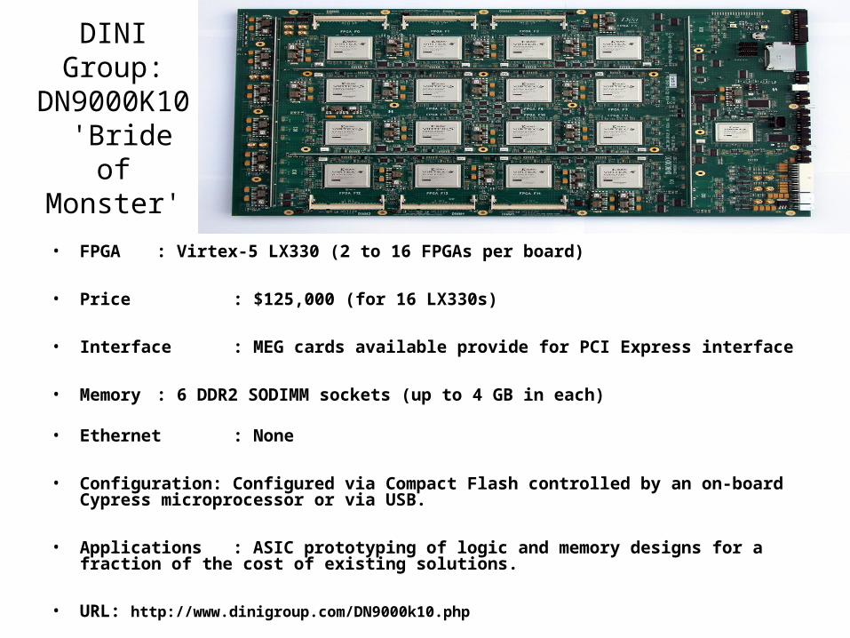
DINI Group: DN9000K10
'Bride of Monster'
• FPGA : Virtex-5 LX330 (2 to 16 FPGAs per board)
• Price : $125,000 (for 16 LX330s)
• Interface : MEG cards available provide for PCI Express interface
• Memory : 6 DDR2 SODIMM sockets (up to 4 GB in each) • Ethernet : None
• Configuration: Configured via Compact Flash controlled by an on-board Cypress microprocessor or via USB.
• Applications : ASIC prototyping of logic and memory designs for a fraction of the cost of existing solutions.
• URL: http://www.dinigroup.com/DN9000k10.php
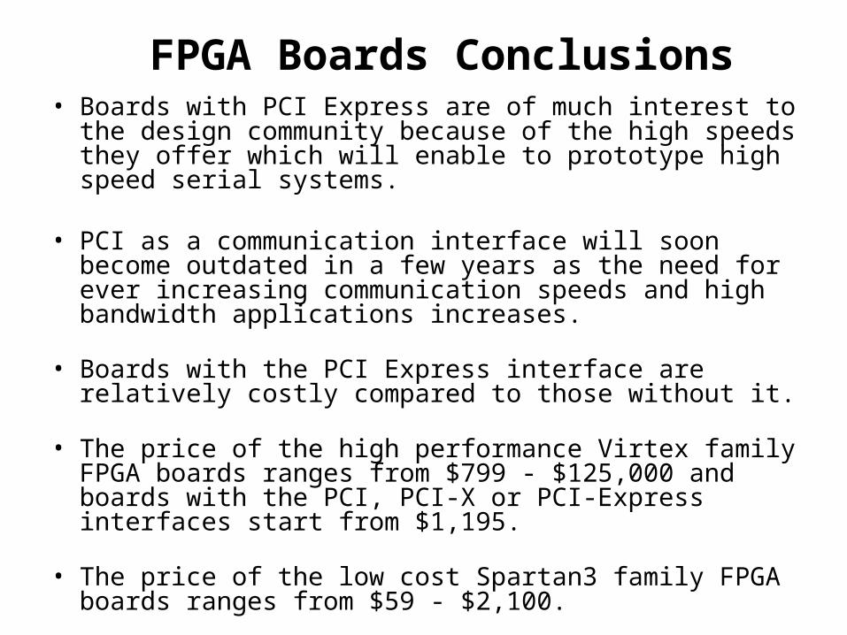
FPGA Boards Conclusions• Boards with PCI Express are of much interest to the
design community because of the high speeds they offer which will enable to prototype high speed serial systems.
• PCI as a communication interface will soon become outdated in a few years as the need for ever increasing communication speeds and high bandwidth applications increases.
• Boards with the PCI Express interface are relatively costly compared to those without it.
• The price of the high performance Virtex family FPGA boards ranges from $799 - $125,000 and boards with the PCI, PCI-X or PCI-Express interfaces start from $1,195.
• The price of the low cost Spartan3 family FPGA boards ranges from $59 - $2,100.

27ECE 448 – FPGA and ASIC Design with VHDL
Behavioral Synthesis

28ECE 448 – FPGA and ASIC Design with VHDL
Behavioral Synthesis
Algorithm
I/O Behavior
Target Library
Behavioral Synthesis
RTL Design
LogicSynthesis
Gate level Netlist
Classic RTL Design Flow

29ECE 448 – FPGA and ASIC Design with VHDL
Need for High-Level Design
• Higher level of abstraction• Modeling complex designs• Reduce design efforts• Fast turnaround time• Technology independence• Ease of HW/SW partitioning

30ECE 448 – FPGA and ASIC Design with VHDL
Advantages of Behavioral Synthesis
• Easy to model higher level of complexities• Smaller in size source compared to RTL code• Generates RTL much faster than manual method• Multi-cycle functionality• Loops• Memory Access
31ECE 448 – FPGA and ASIC Design with VHDL
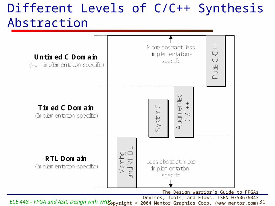
More abstract, lessimplementation-
specific
Less abstract, moreimplementation-
specific
RTL Domain(Implementation-specific)
Timed C Domain(Implementation-specific)
Untimed C Domain(Non-implementation-specific)
Ver
ilog
and
VH
DL
Sys
tem
C
Aug
men
ted
C/C
++
Pur
e C
/C+
+
The Design Warrior’s Guide to FPGAsDevices, Tools, and Flows. ISBN 0750676043
Copyright © 2004 Mentor Graphics Corp. (www.mentor.com)
Different Levels of C/C++ Synthesis Abstraction
32ECE 448 – FPGA and ASIC Design with VHDL
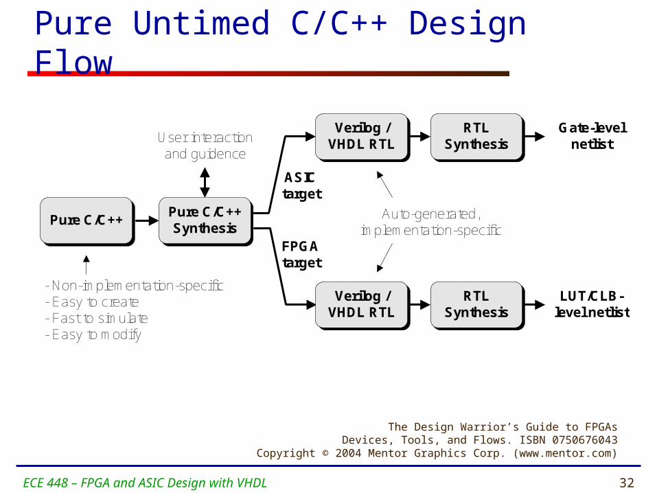
- Non-implementation-specific- Easy to create- Fast to simulate- Easy to modify
Pure C/C++
Gate-levelnetlist
Verilog /VHDL RTL
LUT/CLB-level netlist
ASICtarget
Pure C/C++Synthesis
User interactionand guidence
Verilog /VHDL RTL
RTLSynthesis
RTLSynthesis
FPGAtarget
Auto-generated,implementation-specific
Pure Untimed C/C++ Design Flow
The Design Warrior’s Guide to FPGAsDevices, Tools, and Flows. ISBN 0750676043
Copyright © 2004 Mentor Graphics Corp. (www.mentor.com)
33ECE 448 – FPGA and ASIC Design with VHDL
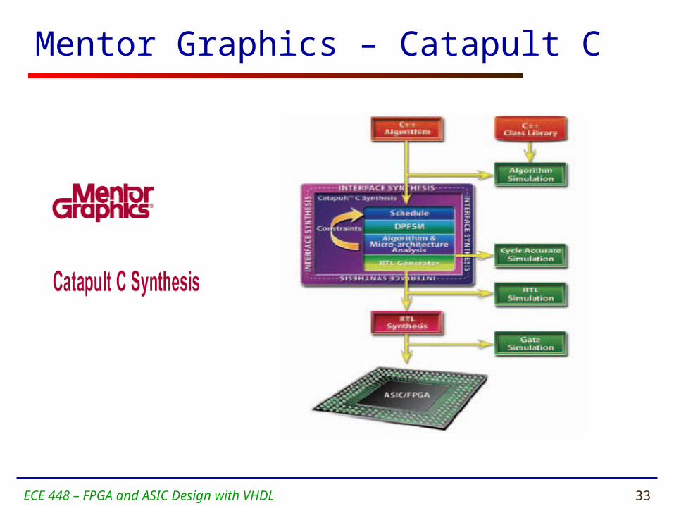
Mentor Graphics – Catapult C

34ECE 448 – FPGA and ASIC Design with VHDL
• Catapult C automatically converts un-timed C/C++ descriptions into synthesizable RTL.
Mentor Graphics – Catapult C

35ECE 448 – FPGA and ASIC Design with VHDL
Hardware-Oriented High-Level Languages
• C-Based System level languages• Commercial
• SystemC -- The Open SystemC Initiative
• Handel C -- Celoxica Ltd.
• Impulse C -- Impulse Accelerated Technologies
• Carte C – SRC Computers
• Research• Streams-C -- Los Alamos National Laboratory
• SA-C -- Colorado State University, University of California, Riverside, Khoral Research, Inc.
• SpecC – University of California, Irvine and SpecC Technology Open Consortium
36ECE 448 – FPGA and ASIC Design with VHDL
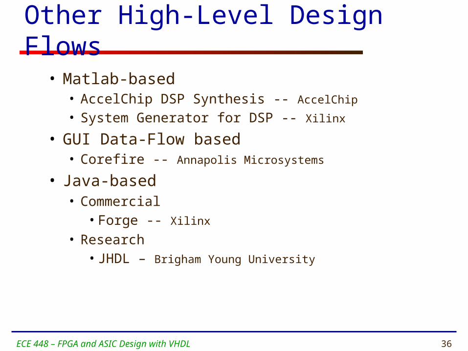
Other High-Level Design Flows
• Matlab-based• AccelChip DSP Synthesis -- AccelChip
• System Generator for DSP -- Xilinx
• GUI Data-Flow based • Corefire -- Annapolis Microsystems
• Java-based• Commercial
• Forge -- Xilinx
• Research• JHDL – Brigham Young University

37ECE 448 – FPGA and ASIC Design with VHDL
SystemC -based design-flow alternatives
SystemC
Auto-RTLTranslation
Verilog / VHDL RTL
RTLSynthesis
SystemCSynthesis
Gate-level netlist
Implementation specific, relatively slow to simulate, relatively difficult to modify
Alternative SystemC flows
38ECE 448 – FPGA and ASIC Design with VHDL
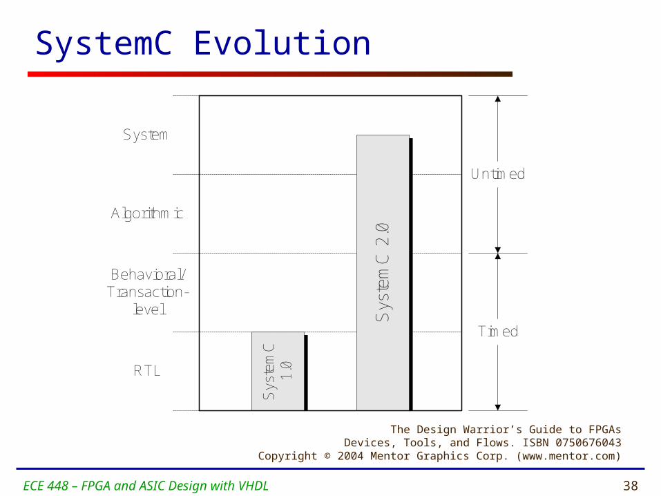
SystemC Evolution
Sys
tem
C 2
.0
Sys
tem
C1.
0RTL
Behavioral/Transaction-
level
Algorithmic
System
Timed
Untimed
The Design Warrior’s Guide to FPGAsDevices, Tools, and Flows. ISBN 0750676043
Copyright © 2004 Mentor Graphics Corp. (www.mentor.com)
39ECE 448 – FPGA and ASIC Design with VHDL
Handel-C Overview
• High-level language based on ISO/ANSI-C for the implementation of algorithms in hardware
• Allows software engineers to design hardware without retraining
• Clean extensions for hardware design including flexible data widths, parallelism and communications
• Well defined timing model• Each statement takes a single clock cycle
• Includes extended operators for bit manipulation, and high-level mathematical macros (including floating point)

40ECE 448 – FPGA and ASIC Design with VHDL
Handel-C/ANSI-C Comparisons
Preprocessorsi.e. #define
Structures
ANSI-C Constructsfor, while, if, switch
Functions
Arrays
Pointers
Arithmetic operators
Bitwise logical operators
Logical operators
ANSI-C Standard Library
Recursion
Floating Point
Handel-C Standard Library
Parallelism
Arbitrary width variables
RAM, ROMSignals
Interfaces
Enhanced bit manipulation
ANSI-C HANDEL-C

41ECE 448 – FPGA and ASIC Design with VHDL
Handel-C Design Flow
Executable Specification
Handel-C
Synthesis
Place & Route
VHDL
EDIFEDIF

42ECE 448 – FPGA and ASIC Design with VHDL
Type Summary
Type Width
char 8 bits
unsigned char 8 bits
short 16 bits
unsigned short 16 bits
long 32 bits
unsigned long 32 bits
int Compiler
unsigned int Compiler
int n n bits
unsigned int n n bits
unsigned n n bits
43ECE 448 – FPGA and ASIC Design with VHDL
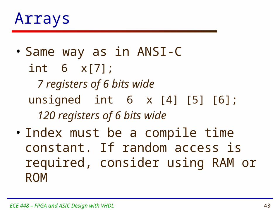
Arrays
• Same way as in ANSI-Cint 6 x[7];
7 registers of 6 bits wide
unsigned int 6 x [4] [5] [6]; 120 registers of 6 bits wide
• Index must be a compile time constant. If random access is required, consider using RAM or ROM
44ECE 448 – FPGA and ASIC Design with VHDL
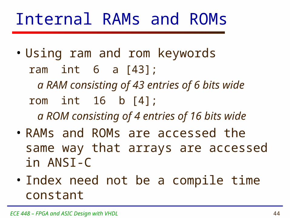
Internal RAMs and ROMs
• Using ram and rom keywordsram int 6 a [43];
a RAM consisting of 43 entries of 6 bits wide
rom int 16 b [4];a ROM consisting of 4 entries of 16 bits wide
• RAMs and ROMs are accessed the same way that arrays are accessed in ANSI-C
• Index need not be a compile time constant
45ECE 448 – FPGA and ASIC Design with VHDL
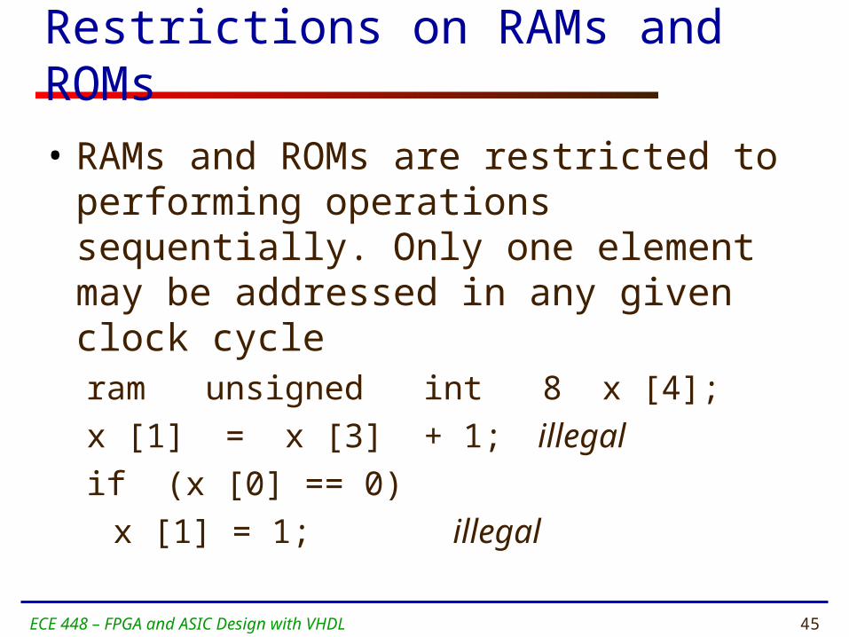
Restrictions on RAMs and ROMs
• RAMs and ROMs are restricted to performing operations sequentially. Only one element may be addressed in any given clock cycleram unsigned int 8 x [4];x [1] = x [3] + 1; illegalif (x [0] == 0)
x [1] = 1; illegal
46ECE 448 – FPGA and ASIC Design with VHDL
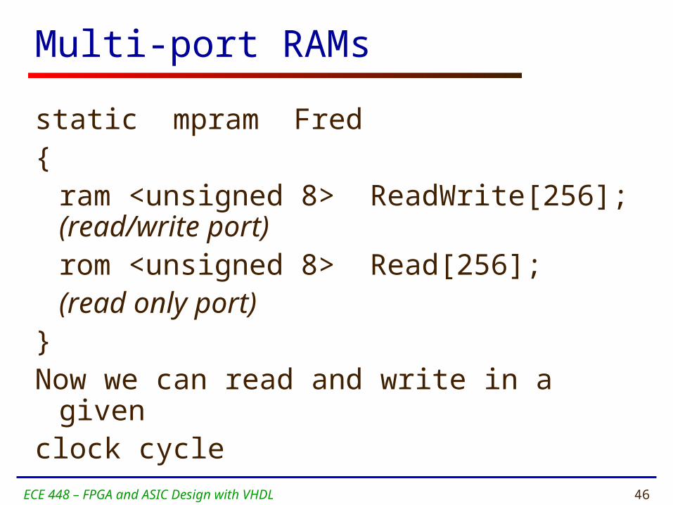
Multi-port RAMs
static mpram Fred{
ram <unsigned 8> ReadWrite[256]; (read/write port)
rom <unsigned 8> Read[256];(read only port)
}Now we can read and write in a given clock cycle
47ECE 448 – FPGA and ASIC Design with VHDL
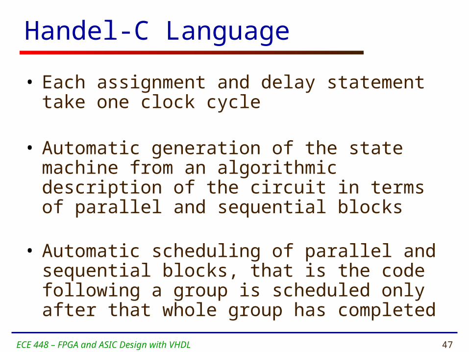
Handel-C Language
• Each assignment and delay statement take one clock cycle
• Automatic generation of the state machine from an algorithmic description of the circuit in terms of parallel and sequential blocks
• Automatic scheduling of parallel and sequential blocks, that is the code following a group is scheduled only after that whole group has completed
48ECE 448 – FPGA and ASIC Design with VHDL
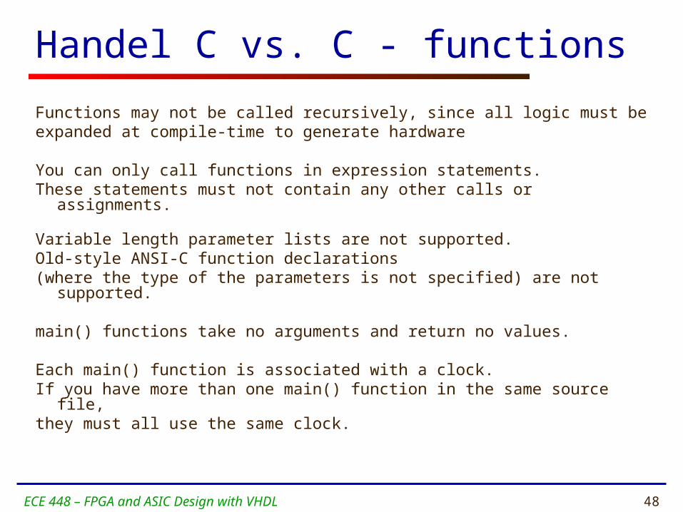
Handel C vs. C - functions
Functions may not be called recursively, since all logic must beexpanded at compile-time to generate hardware
You can only call functions in expression statements. These statements must not contain any other calls or assignments.
Variable length parameter lists are not supported.Old-style ANSI-C function declarations (where the type of the parameters is not specified) are not supported.
main() functions take no arguments and return no values.
Each main() function is associated with a clock. If you have more than one main() function in the same source file,they must all use the same clock.

49
+ very easy to learn and use+ super set of ANSI C+ hides implementation details+ very flexible , no limitation in parallelism and data
type, extended operators for bit manipulation+ well-defined timing model+ portable to a wide range of FPGA devices
- legacy C code requires rewriting
- each statement takes 1 clock cycle to execute
Celoxica Handel-C
50ECE 448 – FPGA and ASIC Design with VHDL
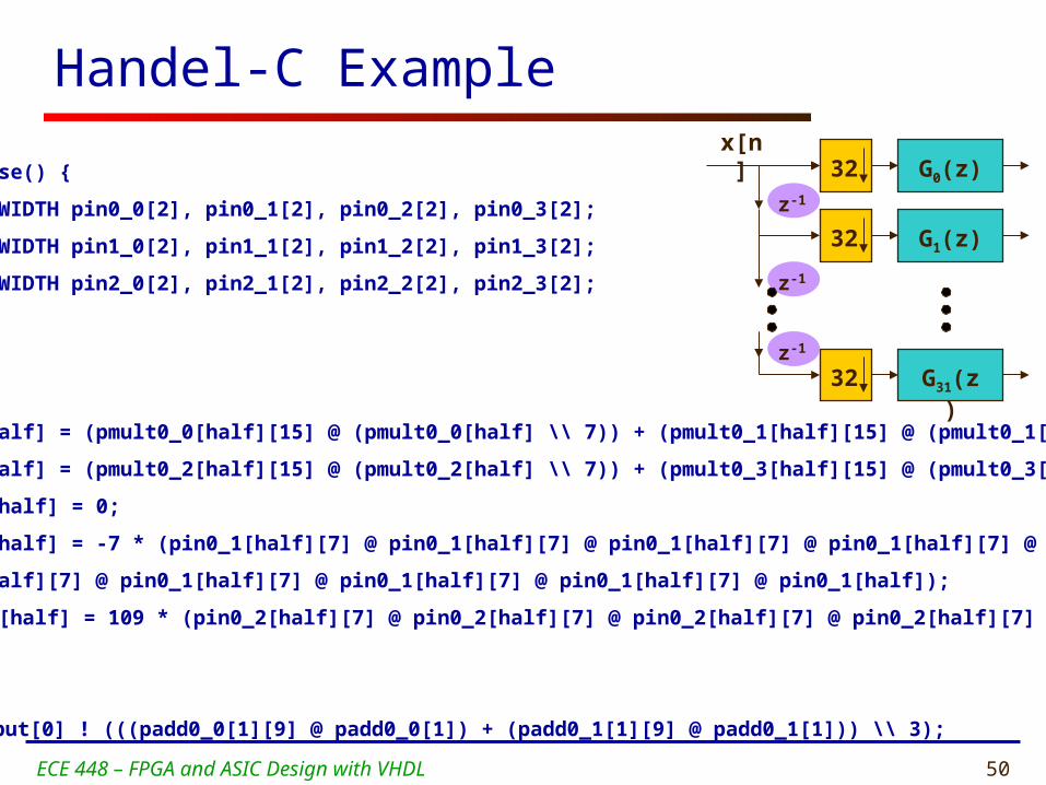
Handel-C Example
32
32
32
x[n]
z-1
z-1
z-1
G31(z)
G1(z)
G0(z)void polyphase() {
ram int IN_WIDTH pin0_0[2], pin0_1[2], pin0_2[2], pin0_3[2];
ram int IN_WIDTH pin1_0[2], pin1_1[2], pin1_2[2], pin1_3[2];
ram int IN_WIDTH pin2_0[2], pin2_1[2], pin2_2[2], pin2_3[2];
…..
while (1) {
par {
padd0_0[half] = (pmult0_0[half][15] @ (pmult0_0[half] \\ 7)) + (pmult0_1[half][15] @ (pmult0_1[half] \\ 7));
padd0_1[half] = (pmult0_2[half][15] @ (pmult0_2[half] \\ 7)) + (pmult0_3[half][15] @ (pmult0_3[half] \\ 7));
pmult0_0[half] = 0;
pmult0_1[half] = -7 * (pin0_1[half][7] @ pin0_1[half][7] @ pin0_1[half][7] @ pin0_1[half][7] @
pin0_1[half][7] @ pin0_1[half][7] @ pin0_1[half][7] @ pin0_1[half][7] @ pin0_1[half]);
pmult0_2[half] = 109 * (pin0_2[half][7] @ pin0_2[half][7] @ pin0_2[half][7] @ pin0_2[half][7] @
if (half) {
par {
output[0] ! (((padd0_0[1][9] @ padd0_0[1]) + (padd0_1[1][9] @ padd0_1[1])) \\ 3);
51ECE 448 – FPGA and ASIC Design with VHDL
Reconfigurable
Supercomputers

52ECE 448 – FPGA and ASIC Design with VHDL
Interface
P memory
P memory
. . .
P P . . .
I/O Interface
FPGA memory
FPGA memory
. . .
FPGA FPGA . . .
I/O
Microprocessor system Reconfigurable system
What is a Reconfigurable Computer?
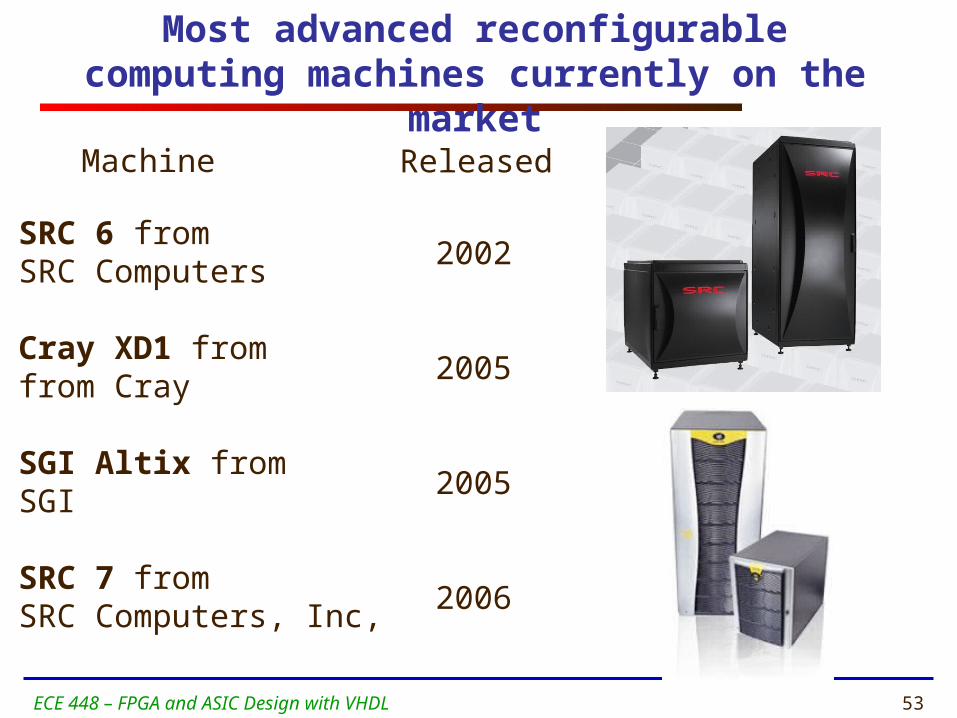
53ECE 448 – FPGA and ASIC Design with VHDL
Most advanced reconfigurablecomputing machines currently on the market
Machine Released
SRC 6 fromSRC Computers
Cray XD1 fromfrom Cray
SGI Altix fromSGI
SRC 7 fromSRC Computers, Inc,
2002
2005
2005
2006
54ECE 448 – FPGA and ASIC Design with VHDL
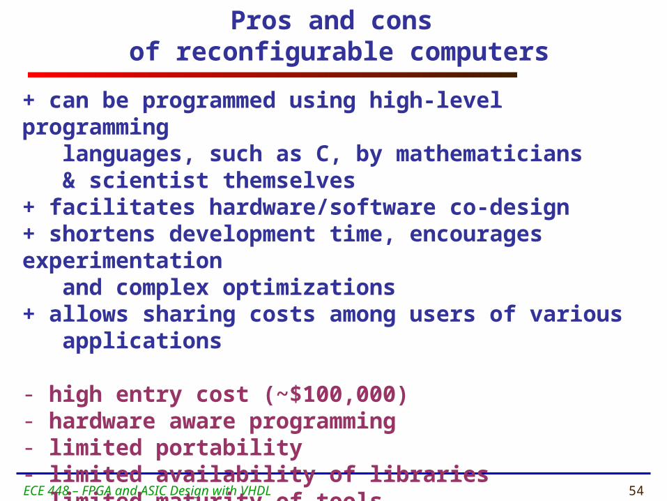
Pros and cons of reconfigurable computers
+ can be programmed using high-level programming languages, such as C, by mathematicians & scientist themselves+ facilitates hardware/software co-design+ shortens development time, encourages experimentation and complex optimizations+ allows sharing costs among users of various applications
- high entry cost (~$100,000)- hardware aware programming- limited portability- limited availability of libraries- limited maturity of tools.
55ECE 448 – FPGA and ASIC Design with VHDL
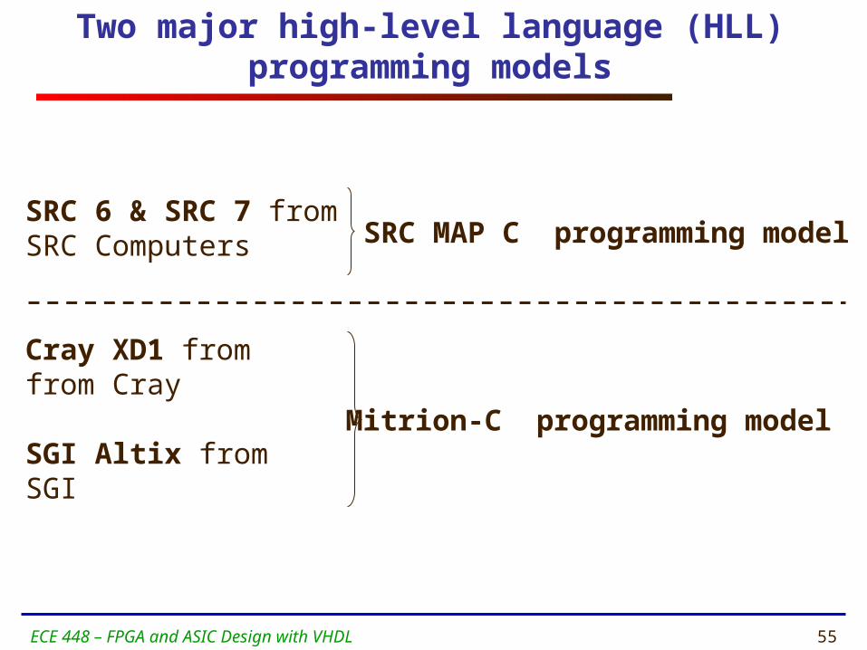
Two major high-level language (HLL)programming models
SRC 6 & SRC 7 fromSRC Computers
Cray XD1 fromfrom Cray
SGI Altix fromSGI
SRC MAP C programming model
Mitrion-C programming model
56ECE 448 – FPGA and ASIC Design with VHDL
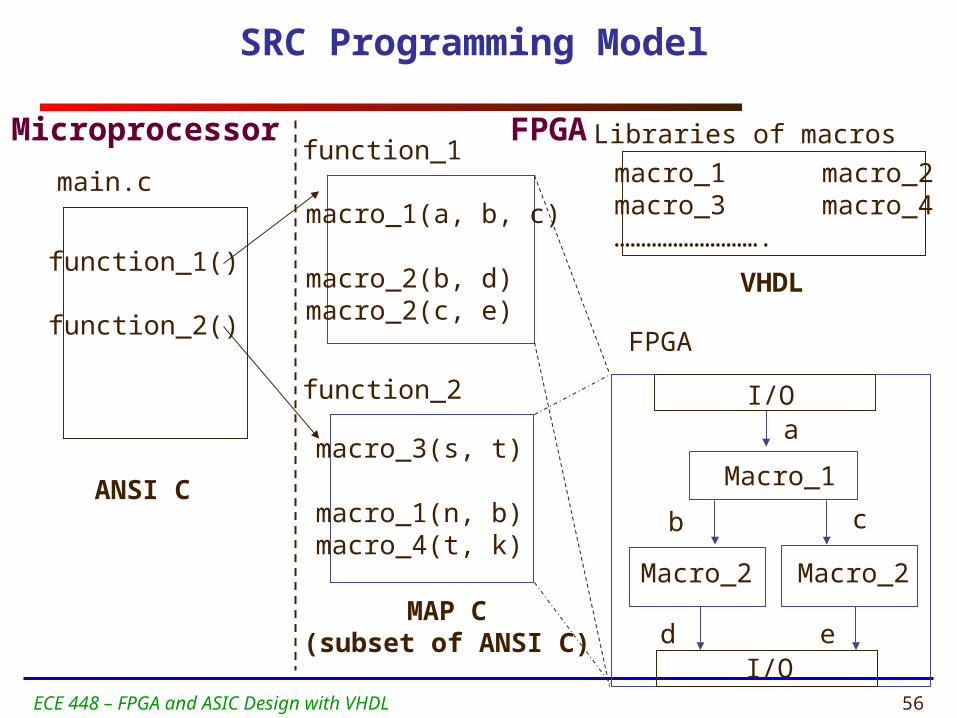
SRC Programming Model
Microprocessor FPGA
main.c
function_1()
function_2()
ANSI C
function_1
function_2
macro_1(a, b, c)
macro_2(b, d)macro_2(c, e)
macro_3(s, t)
macro_1(n, b)macro_4(t, k)
FPGA
Macro_1
Macro_2 Macro_2
a
b c
d eMAP C
(subset of ANSI C)
I/O
I/O
Libraries of macros
VHDL
macro_1 macro_2macro_3 macro_4……………………….
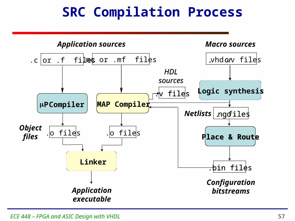
57ECE 448 – FPGA and ASIC Design with VHDL
SRC Compilation Process
Objectfiles
Application sources Macro sources
MAP CompilerP Compiler
Logic synthesis
Place & Route
Linker
.v files
.bin files
.ngo files
.o files .o files
Applicationexecutable
Configurationbitstreams
HDLsources
Netlists
.c or .f files .vhd or .v files
Logic synthesis
Place & Route
Linker
.v files
.bin files
.ngo files
HDLsources
. or.mc or .mf files

58ECE 448 – FPGA and ASIC Design with VHDL
Library Development - SRC
HLL (C, Fortran)
HDL (VHDL, Verilog)
P system
FPGA system
ApplicationProgrammer
LibraryDeveloper
HLL (C, Fortran)
HLL (C, Fortran)
LLL (ASM)
HLL (C, Fortran)

59ECE 448 – FPGA and ASIC Design with VHDL
SRC Programming Environment
+ very easy to learn and use+ standard ANSI C+ hides implementation details+ very well integrated environment+ mature - in production use for over 4 years with constant improvements
- subset of C- legacy C code requires rewriting- C limitations in describing HW (paralellism, data types)- closed environment, limited portability of code to HW platforms other than SRC
60ECE 448 – FPGA and ASIC Design with VHDL
Application Development
for
Reconfigurable
Computers

61ECE 448 – FPGA and ASIC Design with VHDL
Application Developmentfor Reconfigurable Computers
ProgramEntry
Compilation
Execution
Platformmapping
Debugging &Verification

62ECE 448 – FPGA and ASIC Design with VHDL
Program
Program Entry
63ECE 448 – FPGA and ASIC Design with VHDL
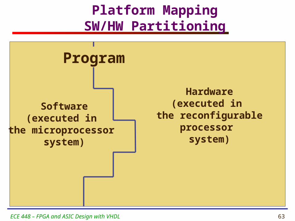
Platform MappingSW/HW Partitioning
Software(executed in
the microprocessor system)
Hardware(executed in
the reconfigurableprocessor
system)
Program

64ECE 448 – FPGA and ASIC Design with VHDL
SW/HW Partitioning & CodingTraditional Approach
Specification
SW/HW Partitioning
SW Coding HW Coding
SW Compilation HW Compilation
SW Profiling HW Profiling

65ECE 448 – FPGA and ASIC Design with VHDL
SW/HW Partitioning & CodingNew Approach
Specification
SW/HW Coding
SW Compilation HW Compilation
SW Profiling HW Profiling
SW/HW Partitioning
66ECE 448 – FPGA and ASIC Design with VHDL
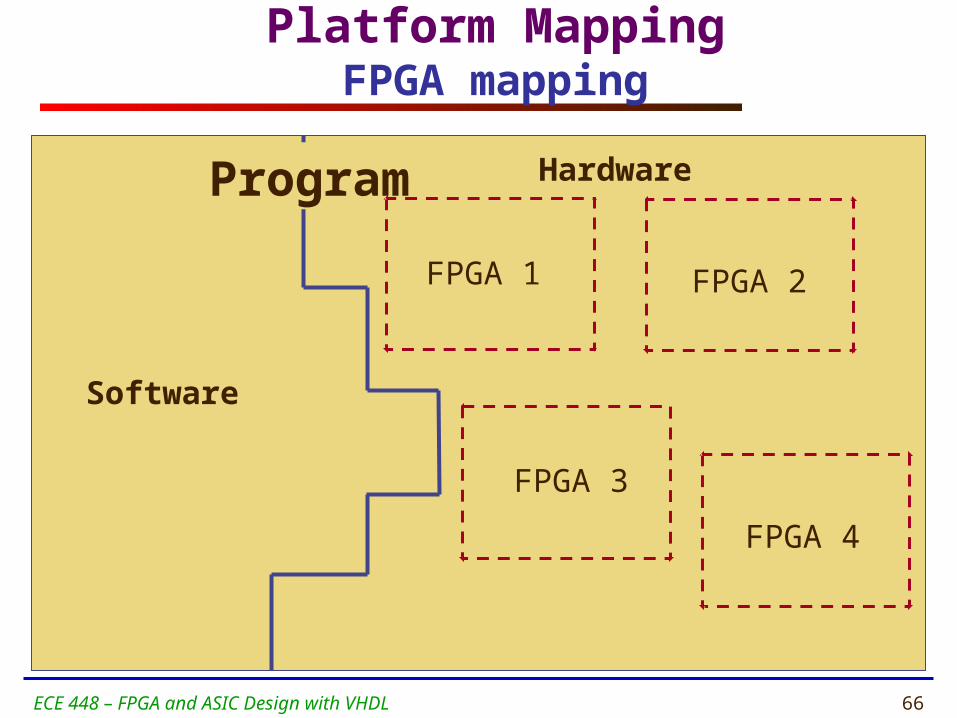
Platform MappingFPGA mapping
Software
HardwareProgram
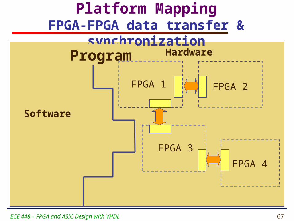
FPGA 1 FPGA 2
FPGA 3
FPGA 4
67ECE 448 – FPGA and ASIC Design with VHDL
Platform MappingFPGA-FPGA data transfer & synchronization
Software
HardwareProgram
FPGA 1 FPGA 2
FPGA 3
FPGA 4
68ECE 448 – FPGA and ASIC Design with VHDL
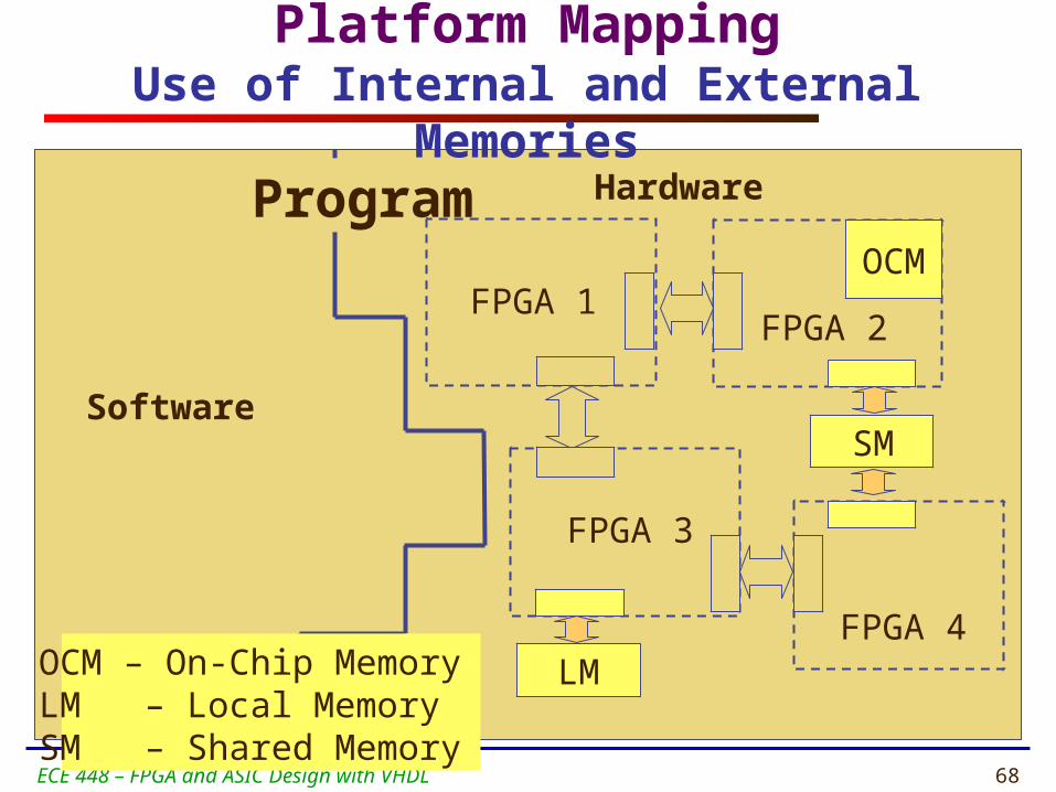
Platform MappingUse of Internal and External Memories
Software
HardwareProgram
FPGA 1FPGA 2
FPGA 3
FPGA 4
OCM
OCM – On-Chip Memory LM – Local Memory SM – Shared Memory
SM
LM

69ECE 448 – FPGA and ASIC Design with VHDL
Platform MappingI/O
Software
HardwareProgram
FPGA 1 FPGA 2
FPGA 3
FPGA 4
SM
LM
OCM
SRC
StarBridge

70ECE 448 – FPGA and ASIC Design with VHDL
Ideal Program Entry
ProgramEntry
Function

71ECE 448 – FPGA and ASIC Design with VHDL
Actual Program Entry
SW/HWPartitioning
Data Transfers& Synchronization
Use of Internaland External Memories
Sequence of Run-time Reconfigurations
Use of FPGAResources
(multipliers,μP cores)
PreferredArchitectures
ProgramEntry
Function
FPGAMapping
SW/HW Interface

72ECE 448 – FPGA and ASIC Design with VHDL
Not Supported
ManualEntry
CompilerAutomated
FPGA-FPGA Partitioning
P-FPGA Partitioning
FPGA-FPGA Data Transfer
P-FPGA Data Transfer
Computation-Data transfer Overlapping
Choosing component version
Evolution and the current status of tools
. . . . . . . . .

73ECE 448 – FPGA and ASIC Design with VHDL
Summary
• Mapping algorithms onto reconfigurable computing systems is a parallel processing problem
• Languages for reconfigurable computers range from high level C/Java to schematic to hardware description languages
• Compilers face a daunting task - extract ILP, pipeline loops, unroll, trade-off area/speed
• Current tool chains have many components unfamiliar to software developers


