Graphene electrodes for organic metal-free light-emitting devices Nathaniel D Robinson, Ludvig Edman and Manish Chhowalla Linköping University Post Print N.B.: When citing this work, cite the original article. Original Publication: Nathaniel D Robinson, Ludvig Edman and Manish Chhowalla, Graphene electrodes for organic metal-free light-emitting devices, 2012, Physica Scripta, (T146), 014023. http://dx.doi.org/10.1088/0031-8949/2012/T146/014023 Copyright: Institute of Physics http://www.iop.org/ Postprint available at: Linköping University Electronic Press http://urn.kb.se/resolve?urn=urn:nbn:se:liu:diva-76203
Transcript
Graphene electrodes for organic metal-free
light-emitting devices
Nathaniel D Robinson, Ludvig Edman and Manish Chhowalla
Linköping University Post Print
N.B.: When citing this work, cite the original article.
Original Publication:
Nathaniel D Robinson, Ludvig Edman and Manish Chhowalla, Graphene electrodes for
1 The Transport and Separations Group, Department of Physics, Chemistry andBiology, Linkoping University, SE-58183 Linkoping, Sweden2 The Organic Photonics and Electronics Group, Department of Physics, UmeaUniversity, SE-90187 Umea, Sweden3 Department of Materials Science and Engineering, Rutgers University, 607 TaylorRoad, Piscataway, New Jersey 08854, USA
Abstract. In addition to its fascinating electrical and mechanical properties,graphene is also an electrochemically stable and transparent electrode material.We demonstrate its applicability as both anode and cathode in a light-emittingelectrochemical cell (LEC), an electrochemical analog to a polymer organic light-emitting diode (POLED). Specifically, we summarize recent progress in carbon-basedmetal-free light-emitting devices enabled by chemically-derived graphene cathodeson quartz and plastic substrates, and explain the advantages of using LECs inmanufacturing large-area devices.
1. Introduction
“Organic electronics” has long been defined to encompass devices that include some
electronically-active organic component, i.e. nearly all of todays “organic” light-
emitting devices include two inorganic electrodes to contact an organic emissive layer.
Still, the attractive properties of organic materials, specifically, the relatively small
cost of solution-based manufacturing (via printing and coating), mechanical flexibility
and ability to tune color and other parameters through chemistry, have motivated a
tremendous investment in the development of new and improved organic materials for
the realization of true all-organic devices. Here, we show that the advent of graphene,
with its combination of transparency, conductivity and chemical stability, opens the
possibility of metal-free all-organic light-emitting devices. [1, 2]
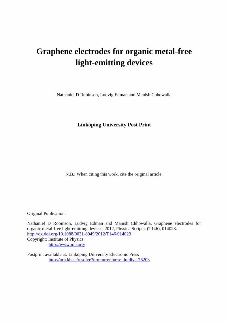
We review our recent progress regarding the use of chemically derived graphene
(CDG) as a transparent electrode in polymer light-emitting electrochemical cells (LECs).
A schematic of the most practical device demonstrated to date, in which a blend of a
light-emitting polymer (LEP) and an electrolyte is sandwiched between a CDG cathode
and conducting polymer anode, is shown in figure 1.
Graphene electrodes for organic metal-free light-emitting devices 2
anode
p-n junction
graphene cathodesubstrate
p-doped region
n-doped region
}
}
PEDOT
PSS- H+Super Yellow
PEO
OC10H21
OC10H21
OC10H21
OC10H21
x
zy
S
O O
n
On
O–S
F
F
F
O
O K+
SO3- H+
Figure 1. Schematic of the metal-free LEC as published in Matyba et al. [1] Copyright2010 ACS. Reused with permission.
1.1. Transparent, metal-free electrodes
The vast majority of solid-state light-emitting devices require a transparent electrode for
operation, as do displays (e.g. liquid crystal displays, LCDs) and photovoltaic devices
(solar panels). “Organic” light-emitting devices have long used indium tin oxide (ITO)
as a highly-transparent, conducting anode [3, 4]. For the case of polymer light-emitting
devices, a metal cathode with a low work function has also been necessary for the
attainment of facile electron injection and efficient device operation. [5]
The development of scalable processes for manufacturing large-area transparent
electrodes based on CDG represents a breakthrough in this field from a processing
perspective, and more importantly a materials perspective. The demand for ITO and
similar materials is increasing as consumer electronics become more popular, imparting
pressure on both the supply (particularly of In) and recycling technology (which is
currently insufficient for handling the large volume of these materials incorporated
into electronic devices). Using carbon-based graphene solves both problems, as the
raw material is seemingly endless on this planet and recycling of carbon-based metal-
free electronic devices can be as simple as burning them to recover the energy in the
materials, yielding little other than water and carbon dioxide.
Graphene electrodes for organic metal-free light-emitting devices 3
(a) Graphene
n
(b) poly(para-phenylenevinylene) (PPV)
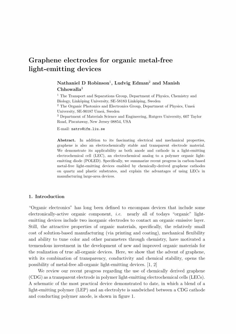
Figure 2. Graphene (left) is an example of an ordered two-dimensional π-conjugatedsystem. PPV (right) is a one-dimensional π-conjugated system when diluted in asolvent, but intrachain and interchain interactions increase the dimensionality of theπ-system in solid films.
1.2. Organic electronics
The current effort to develop electronic components such as lamps, displays, sensors,
solar cells and control systems based on organic molecules and polymers for currently
“inactive” space is tremendous. Billions of dollars of research and development are
pushing to bring new functionality to areas such as consumer packaging and the walls
of your home and office. During the past 20 to 30 years, tremendous progress has been
made in advancing materials and devices to meet this challenge.
One category of organic electronics, in which polymeric (plastic) materials are
primarily used, has several particular advantages. Like nearly all organic electronic
materials, polymers are synthetic, so they can be customized and tailored to include
a wide variety of functionality. However, polymers are also often solution processable,
meaning that they can be dissolved or suspended in a solvent, forming an “ink-like”
material that can be coated or printed with a variety of techniques. This makes polymer
electronic materials very easy, and therefore inexpensive, to process.
The conductivity in these polymers comes from an extended π-structure along the
backbone. A series of alternating single and double C-C bonds causes this so-called
π-conjugation. Just as graphene has a two-dimensional π-system, giving rise to its
incredible electronic properties, a π-conjugated polymer has a similar one-dimensional
system along its backbone. Figure 2 shows the two structures side-by-side. Note that
in the bulk of a solid film, where the conjugated polymer is intertwined with both
itself and neighboring polymer chains, intrachain and interchain interactions increase
the dimensionality of the conjugated system. Many conjugated polymers are highly
fluorescent, and the emission color (and other characteristics) of these LEPs can be
tailored during synthesis by, e.g., adding various side-chains to the polymer backbone.
Derivatives of, and copolymers containing, poly(para-phenylene vinylene) (PPV) are
commonly used in emissive applications, but many other classes of LEPs are also
available. [6]
Graphene electrodes for organic metal-free light-emitting devices 4
Substrate (quartz or PET)
Cathode (Ca/Al or LiF/Al)
Light-emitting polymer
Anode (ITO or graphene)
(a) POLED
Substrate (quartz or PET)
Cathode (Al)
LEP and polymer electrolyte
Anode (ITO or graphene)
(b) “Sandwich” LEC
Substrate (quartz or PET)
LEP and polymer electrolyteElectrodes (graphene)
(c) Planar LEC
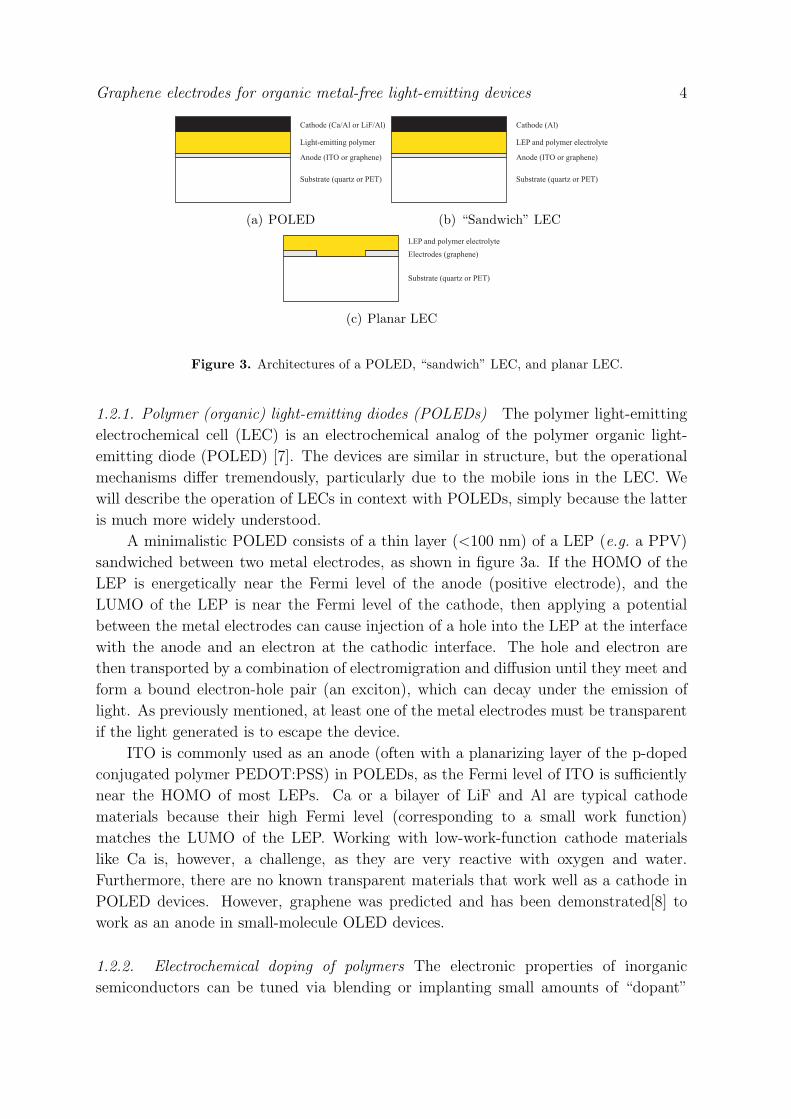
Figure 3. Architectures of a POLED, “sandwich” LEC, and planar LEC.
1.2.1. Polymer (organic) light-emitting diodes (POLEDs) The polymer light-emitting
electrochemical cell (LEC) is an electrochemical analog of the polymer organic light-
emitting diode (POLED) [7]. The devices are similar in structure, but the operational
mechanisms differ tremendously, particularly due to the mobile ions in the LEC. We
will describe the operation of LECs in context with POLEDs, simply because the latter
is much more widely understood.
A minimalistic POLED consists of a thin layer (<100 nm) of a LEP (e.g. a PPV)
sandwiched between two metal electrodes, as shown in figure 3a. If the HOMO of the
LEP is energetically near the Fermi level of the anode (positive electrode), and the
LUMO of the LEP is near the Fermi level of the cathode, then applying a potential
between the metal electrodes can cause injection of a hole into the LEP at the interface
with the anode and an electron at the cathodic interface. The hole and electron are
then transported by a combination of electromigration and diffusion until they meet and
form a bound electron-hole pair (an exciton), which can decay under the emission of
light. As previously mentioned, at least one of the metal electrodes must be transparent
if the light generated is to escape the device.
ITO is commonly used as an anode (often with a planarizing layer of the p-doped
conjugated polymer PEDOT:PSS) in POLEDs, as the Fermi level of ITO is sufficiently
near the HOMO of most LEPs. Ca or a bilayer of LiF and Al are typical cathode
materials because their high Fermi level (corresponding to a small work function)
matches the LUMO of the LEP. Working with low-work-function cathode materials
like Ca is, however, a challenge, as they are very reactive with oxygen and water.
Furthermore, there are no known transparent materials that work well as a cathode in
POLED devices. However, graphene was predicted and has been demonstrated[8] to
work as an anode in small-molecule OLED devices.
1.2.2. Electrochemical doping of polymers The electronic properties of inorganic
semiconductors can be tuned via blending or implanting small amounts of “dopant”
Graphene electrodes for organic metal-free light-emitting devices 5
materials with differing valence into the host semiconductor, which effectively
donate/accept an electron to/from the semiconductor host. This chemical doping results
in the formation of conducting doped regions, which, for instance, can be utilized for
the realization of high-speed transistors that are the basis for the microprocessors and
memory chips in today’s personal computers.
Conjugated polymers can also be chemically doped by adding appropriate oxidizing
or reducing agents to the polymer, resulting in a “permanently” doped material.
Alternatively, when the conjugated polymer is in contact with mobile ions and an
electrode, it can be doped electrochemically, in situ. The ions can come from a salt
added directly to the polymer if the polymer can dissolve it, but usually a solid-state
solvent such as polyethyleneoxide (PEO) is required. The doping process can either be
of p-type:
P + X− � P+X− + e− (1)
where P represents the undoped polymer, X− represents an anion (from the salt M+X−),
P+ represents (a segment of) p-doped polymer and e− represents an electron; or of n-
type:
P + M+ + e− � M+P− (2)
where M+ represents a cation from the dissolved salt and P− represents (a segment of)
n-doped polymer.
As with inorganic semiconducting materials, doping a polymer semiconductor can
change its conductivity several orders of magnitude. [9, 10] The polymers also typically
change color [11, 12] and size, [13, 14] and their surface chemistry alters [15, 16, 17]
during the doping process. In general, many “field-effect” (ion-free) polymer devices
have electrochemical analogs. [10].
1.3. The light-emitting electrochemical cell (LEC)
Blending an ion-solving material such as PEO and a salt (e.g. KCF3SO3) with the LEP,
and fabricating the same sandwich structure previously described creates an LEC. The
mobile ions serve several functions. First, they assist charge injection. When a potential
is applied between the electrodes, the anions and cations electromigrate (drift) toward
the anode and cathode, respectively. The metal electrode is impermeable to ions, so the
ions congregate in a dense layer of high charge density at the interface, with an equal and
opposite charge density in the metal electrode itself, forming a so-called electric double-
layer. This double-layer has a thickness on the order of the Debye screening length which
is typically around 1 nm, and which is short enough for tunneling of electrons through
the double-layer to be significant. Thus, the difference in energy between the LEP’s
HOMO and LUMO and the Fermi level of the anode and cathode are no longer critical
to the operation of the device (although they can still affect the device [18, 19]). In other
words, efficient LECs can be made with a much wider variety of electrode materials than
POLEDs. In fact, the same material can often be used for both electrodes. [20, 21, 22]
Graphene electrodes for organic metal-free light-emitting devices 6
Once charge injection into the LEP layer occurs, the introduction of mobile
electrons/holes in combination with the existence of mobile ions allows electrochemical
doping to occur (see (1) and (2)). Thus, the LEP becomes p-doped near the anode and
n-doped near the cathode. This converts the polymer to a (relatively good) conductor,
extending the effective anode and cathode into the LEP. This process continues and
the doped regions expand toward one another until they meet, forming a p-n (or p-i-
n) junction. At this point, the device turns on, as holes and electrons can meet and
recombine in the narrow strip of undoped material between the two doped regions.
One desirable consequence of this doping process is that LEC operation is relatively
independent of the thickness of the active layer. Thicker devices require more time to
turn on, but can still operate at potentials at or slightly above the bandgap of the LEP
[23]. POLEDs, on the other hand, are field-dependent, which means that the voltage
required to operate the device increases with the thickness of the LEP layer. Low-
voltage devices are desirable, particularly for battery-powered portable systems, while
“thick” layers (> 500 nm) are relatively easy to manufacture with coating and printing
equipment and processes. Thinner layers are more susceptible to pinhole defects that
cause short-circuits, rendering a device inoperable. This challenge becomes particularly
important with increasing device area, where even extremely low defect densities (e.g.
those found in the silicon semiconductor industry) become unacceptable.
The device thickness can be taken to extremes. For example, rather than making a
sandwich structure, one can make a planar device like the one shown in figure 3c. In this
device, the gap between the electrodes (which are usually the same material) can be up
to several mm [24, 21, 22, 19, 25]. This allows the doping progression described above to
be followed over time due to the sharp contrast between the photoluminescent undoped
LEP and the doped LEP where the photoluminescence is quenched. [24] Furthermore,
the surface potential within the device can be measured via scanning kelvin probe
microscopy (SKPM). [26, 27, 28] See Robinson et al. [22, 25] and Matyba et al. [28]
for measurements, analysis and discussion of the turn-on process in wide-gap devices.
1.3.1. Metal-free LECs Several opportunities arise because LECs are compatible with
a wider range of electrode materials than OLEDs. For example, high-work-function
materials such as graphene can be used as both the anode and cathode, eliminating
the need for both the ITO and the reactive metal found in the vast majority of
OLED devices. [1] Other carbon allotropes such as carbon nanotubes, have also been
demonstrated as transparent electrodes in polymer LECs. [29]
2. Preparation of electrodes
A summary of the preparation of the electrodes is provided here. For details, we refer
to several previous publications. [1, 2]
Graphene electrodes for organic metal-free light-emitting devices 7
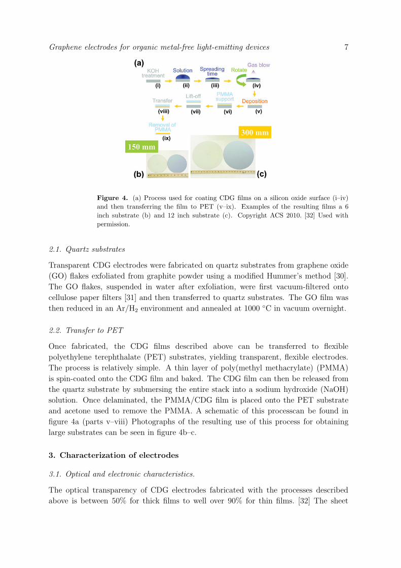
Figure 4. (a) Process used for coating CDG films on a silicon oxide surface (i–iv)and then transferring the film to PET (v–ix). Examples of the resulting films a 6inch substrate (b) and 12 inch substrate (c). Copyright ACS 2010. [32] Used withpermission.
2.1. Quartz substrates
Transparent CDG electrodes were fabricated on quartz substrates from graphene oxide
(GO) flakes exfoliated from graphite powder using a modified Hummer’s method [30].
The GO flakes, suspended in water after exfoliation, were first vacuum-filtered onto
cellulose paper filters [31] and then transferred to quartz substrates. The GO film was
then reduced in an Ar/H2 environment and annealed at 1000 ◦C in vacuum overnight.
2.2. Transfer to PET
Once fabricated, the CDG films described above can be transferred to flexible
The process is relatively simple. A thin layer of poly(methyl methacrylate) (PMMA)
is spin-coated onto the CDG film and baked. The CDG film can then be released from
the quartz substrate by submersing the entire stack into a sodium hydroxide (NaOH)
solution. Once delaminated, the PMMA/CDG film is placed onto the PET substrate
and acetone used to remove the PMMA. A schematic of this processcan be found in
figure 4a (parts v–viii) Photographs of the resulting use of this process for obtaining
large substrates can be seen in figure 4b–c.
3. Characterization of electrodes
3.1. Optical and electronic characteristics.
The optical transparency of CDG electrodes fabricated with the processes described
above is between 50% for thick films to well over 90% for thin films. [32] The sheet
Graphene electrodes for organic metal-free light-emitting devices 8
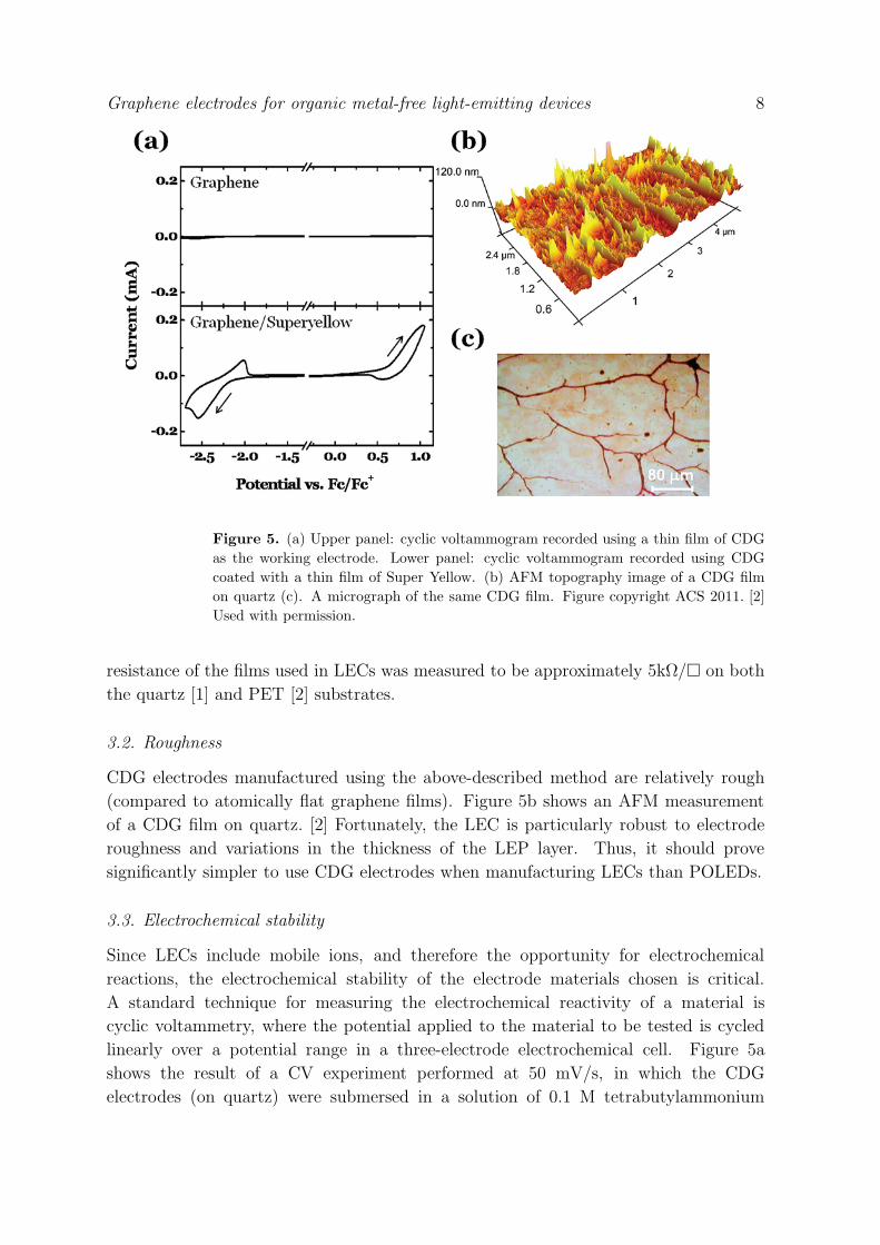
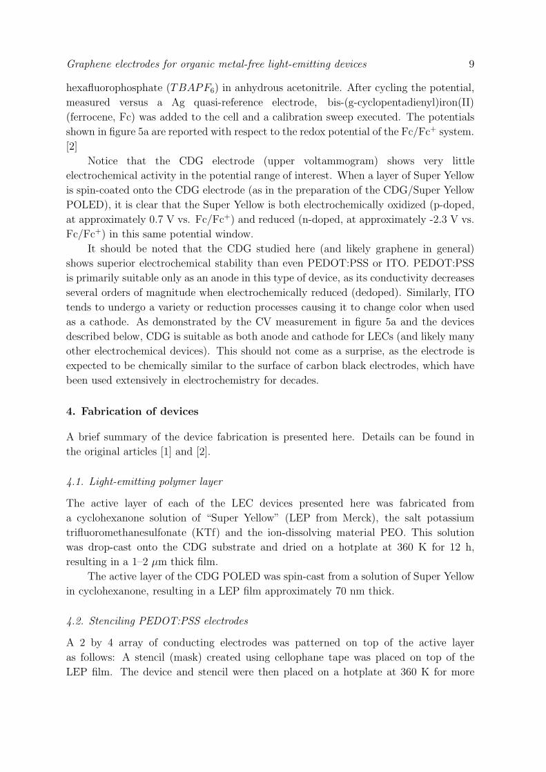
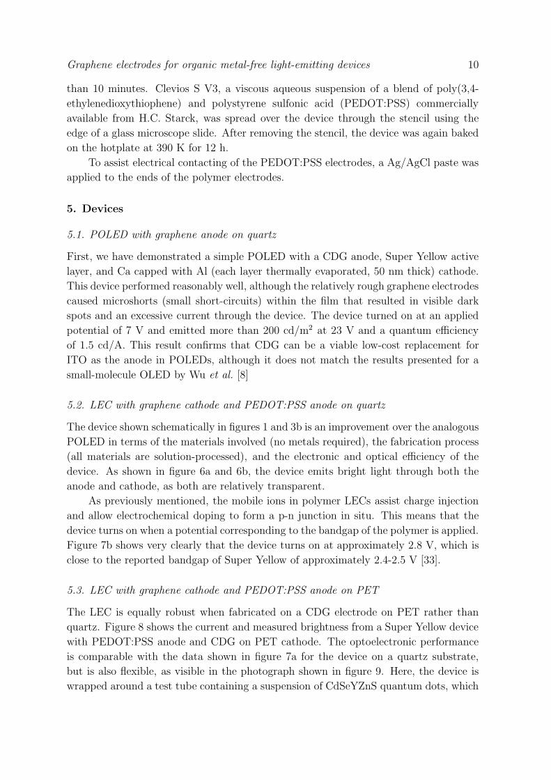
Figure 5. (a) Upper panel: cyclic voltammogram recorded using a thin film of CDGas the working electrode. Lower panel: cyclic voltammogram recorded using CDGcoated with a thin film of Super Yellow. (b) AFM topography image of a CDG filmon quartz (c). A micrograph of the same CDG film. Figure copyright ACS 2011. [2]Used with permission.
resistance of the films used in LECs was measured to be approximately 5kΩ/� on both
the quartz [1] and PET [2] substrates.
3.2. Roughness
CDG electrodes manufactured using the above-described method are relatively rough
(compared to atomically flat graphene films). Figure 5b shows an AFM measurement
of a CDG film on quartz. [2] Fortunately, the LEC is particularly robust to electrode
roughness and variations in the thickness of the LEP layer. Thus, it should prove
significantly simpler to use CDG electrodes when manufacturing LECs than POLEDs.
3.3. Electrochemical stability
Since LECs include mobile ions, and therefore the opportunity for electrochemical
reactions, the electrochemical stability of the electrode materials chosen is critical.
A standard technique for measuring the electrochemical reactivity of a material is
cyclic voltammetry, where the potential applied to the material to be tested is cycled
linearly over a potential range in a three-electrode electrochemical cell. Figure 5a
shows the result of a CV experiment performed at 50 mV/s, in which the CDG
electrodes (on quartz) were submersed in a solution of 0.1 M tetrabutylammonium
Graphene electrodes for organic metal-free light-emitting devices 9
hexafluorophosphate (TBAPF6) in anhydrous acetonitrile. After cycling the potential,
measured versus a Ag quasi-reference electrode, bis-(g-cyclopentadienyl)iron(II)
(ferrocene, Fc) was added to the cell and a calibration sweep executed. The potentials
shown in figure 5a are reported with respect to the redox potential of the Fc/Fc+ system.
[2]
Notice that the CDG electrode (upper voltammogram) shows very little
electrochemical activity in the potential range of interest. When a layer of Super Yellow
is spin-coated onto the CDG electrode (as in the preparation of the CDG/Super Yellow
POLED), it is clear that the Super Yellow is both electrochemically oxidized (p-doped,
at approximately 0.7 V vs. Fc/Fc+) and reduced (n-doped, at approximately -2.3 V vs.
Fc/Fc+) in this same potential window.
It should be noted that the CDG studied here (and likely graphene in general)
shows superior electrochemical stability than even PEDOT:PSS or ITO. PEDOT:PSS
is primarily suitable only as an anode in this type of device, as its conductivity decreases
several orders of magnitude when electrochemically reduced (dedoped). Similarly, ITO
tends to undergo a variety or reduction processes causing it to change color when used
as a cathode. As demonstrated by the CV measurement in figure 5a and the devices
described below, CDG is suitable as both anode and cathode for LECs (and likely many
other electrochemical devices). This should not come as a surprise, as the electrode is
expected to be chemically similar to the surface of carbon black electrodes, which have
been used extensively in electrochemistry for decades.
4. Fabrication of devices
A brief summary of the device fabrication is presented here. Details can be found in
the original articles [1] and [2].
4.1. Light-emitting polymer layer
The active layer of each of the LEC devices presented here was fabricated from
a cyclohexanone solution of “Super Yellow” (LEP from Merck), the salt potassium
trifluoromethanesulfonate (KTf) and the ion-dissolving material PEO. This solution
was drop-cast onto the CDG substrate and dried on a hotplate at 360 K for 12 h,
resulting in a 1–2 μm thick film.
The active layer of the CDG POLED was spin-cast from a solution of Super Yellow
in cyclohexanone, resulting in a LEP film approximately 70 nm thick.
4.2. Stenciling PEDOT:PSS electrodes
A 2 by 4 array of conducting electrodes was patterned on top of the active layer
as follows: A stencil (mask) created using cellophane tape was placed on top of the
LEP film. The device and stencil were then placed on a hotplate at 360 K for more
Graphene electrodes for organic metal-free light-emitting devices 10
than 10 minutes. Clevios S V3, a viscous aqueous suspension of a blend of poly(3,4-
ethylenedioxythiophene) and polystyrene sulfonic acid (PEDOT:PSS) commercially
available from H.C. Starck, was spread over the device through the stencil using the
edge of a glass microscope slide. After removing the stencil, the device was again baked
on the hotplate at 390 K for 12 h.
To assist electrical contacting of the PEDOT:PSS electrodes, a Ag/AgCl paste was
applied to the ends of the polymer electrodes.
5. Devices
5.1. POLED with graphene anode on quartz
First, we have demonstrated a simple POLED with a CDG anode, Super Yellow active
layer, and Ca capped with Al (each layer thermally evaporated, 50 nm thick) cathode.
This device performed reasonably well, although the relatively rough graphene electrodes
caused microshorts (small short-circuits) within the film that resulted in visible dark
spots and an excessive current through the device. The device turned on at an applied
potential of 7 V and emitted more than 200 cd/m2 at 23 V and a quantum efficiency
of 1.5 cd/A. This result confirms that CDG can be a viable low-cost replacement for
ITO as the anode in POLEDs, although it does not match the results presented for a
small-molecule OLED by Wu et al. [8]
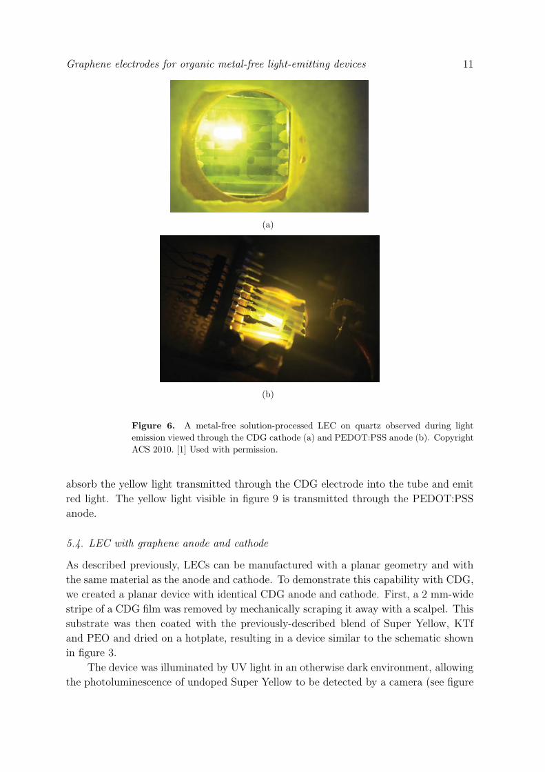
5.2. LEC with graphene cathode and PEDOT:PSS anode on quartz
The device shown schematically in figures 1 and 3b is an improvement over the analogous
POLED in terms of the materials involved (no metals required), the fabrication process
(all materials are solution-processed), and the electronic and optical efficiency of the
device. As shown in figure 6a and 6b, the device emits bright light through both the
anode and cathode, as both are relatively transparent.
As previously mentioned, the mobile ions in polymer LECs assist charge injection
and allow electrochemical doping to form a p-n junction in situ. This means that the
device turns on when a potential corresponding to the bandgap of the polymer is applied.
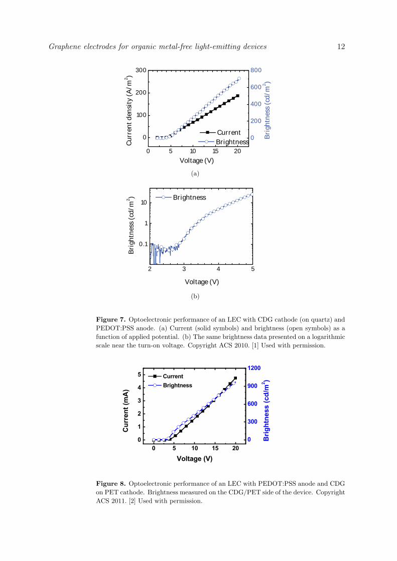
Figure 7b shows very clearly that the device turns on at approximately 2.8 V, which is
close to the reported bandgap of Super Yellow of approximately 2.4-2.5 V [33].
5.3. LEC with graphene cathode and PEDOT:PSS anode on PET
The LEC is equally robust when fabricated on a CDG electrode on PET rather than
quartz. Figure 8 shows the current and measured brightness from a Super Yellow device
with PEDOT:PSS anode and CDG on PET cathode. The optoelectronic performance
is comparable with the data shown in figure 7a for the device on a quartz substrate,
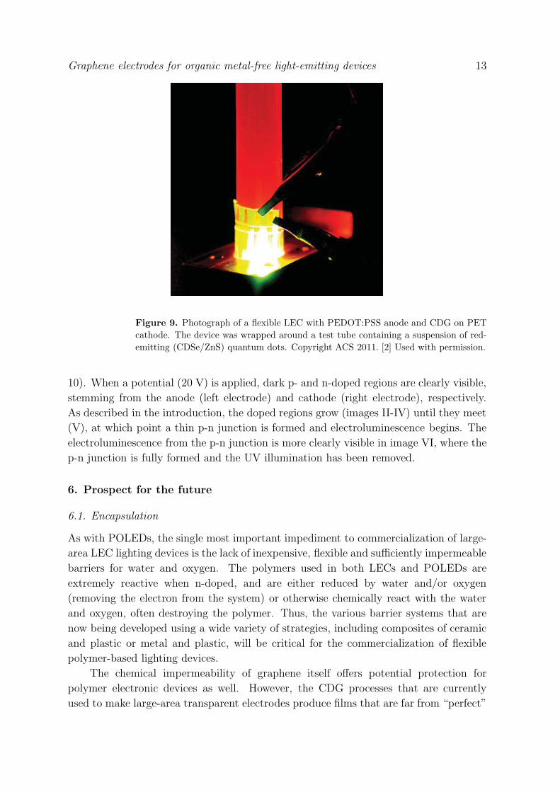
but is also flexible, as visible in the photograph shown in figure 9. Here, the device is
wrapped around a test tube containing a suspension of CdSeYZnS quantum dots, which
Graphene electrodes for organic metal-free light-emitting devices 11
(a)
(b)
Figure 6. A metal-free solution-processed LEC on quartz observed during lightemission viewed through the CDG cathode (a) and PEDOT:PSS anode (b). CopyrightACS 2010. [1] Used with permission.
absorb the yellow light transmitted through the CDG electrode into the tube and emit
red light. The yellow light visible in figure 9 is transmitted through the PEDOT:PSS
anode.
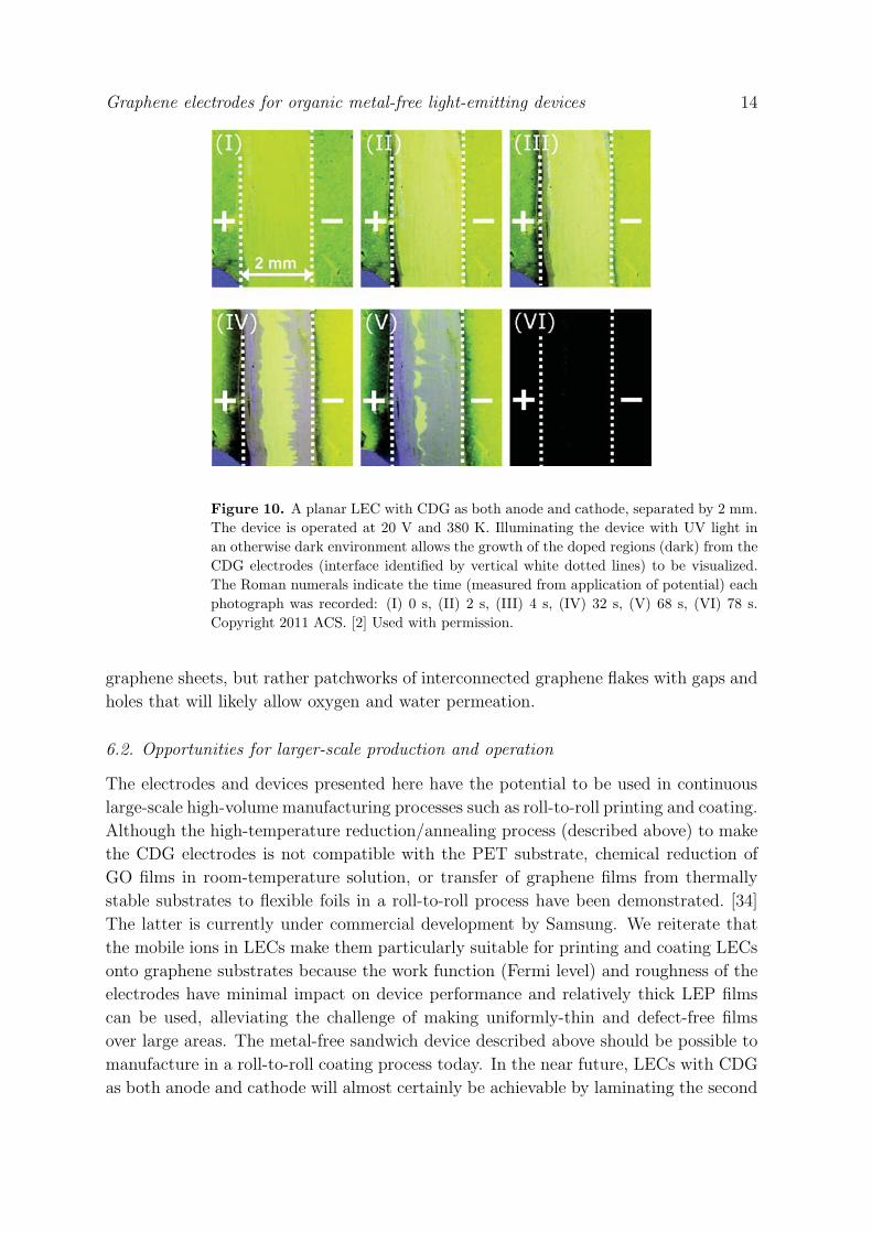
5.4. LEC with graphene anode and cathode
As described previously, LECs can be manufactured with a planar geometry and with
the same material as the anode and cathode. To demonstrate this capability with CDG,
we created a planar device with identical CDG anode and cathode. First, a 2 mm-wide
stripe of a CDG film was removed by mechanically scraping it away with a scalpel. This
substrate was then coated with the previously-described blend of Super Yellow, KTf
and PEO and dried on a hotplate, resulting in a device similar to the schematic shown
in figure 3.
The device was illuminated by UV light in an otherwise dark environment, allowing
the photoluminescence of undoped Super Yellow to be detected by a camera (see figure
Graphene electrodes for organic metal-free light-emitting devices 12
0
200
400
600
800
0 5 10 15 20
0
100
200
300
Current
Cu
rren
t d
ensi
ty (
A/m
2 )
Voltage (V)
Brightness Bri
ghtn
ess
(cd
/m2 )
(a)
2 3 4 5
0.1
1
10
Brightness
Bri
ghtn
ess
(cd
/m2 )
Voltage (V)
(b)
Figure 7. Optoelectronic performance of an LEC with CDG cathode (on quartz) andPEDOT:PSS anode. (a) Current (solid symbols) and brightness (open symbols) as afunction of applied potential. (b) The same brightness data presented on a logarithmicscale near the turn-on voltage. Copyright ACS 2010. [1] Used with permission.
0
300
600
900
1200
0 5 10 15 200
1
2
3
4
5 Current
Cur
rent
(mA
)
Voltage (V)
Brightness
Brig
htne
ss (c
d/m
2 )
Figure 8. Optoelectronic performance of an LEC with PEDOT:PSS anode and CDGon PET cathode. Brightness measured on the CDG/PET side of the device. CopyrightACS 2011. [2] Used with permission.
Graphene electrodes for organic metal-free light-emitting devices 13
Figure 9. Photograph of a flexible LEC with PEDOT:PSS anode and CDG on PETcathode. The device was wrapped around a test tube containing a suspension of red-emitting (CDSe/ZnS) quantum dots. Copyright ACS 2011. [2] Used with permission.
10). When a potential (20 V) is applied, dark p- and n-doped regions are clearly visible,
stemming from the anode (left electrode) and cathode (right electrode), respectively.
As described in the introduction, the doped regions grow (images II-IV) until they meet
(V), at which point a thin p-n junction is formed and electroluminescence begins. The
electroluminescence from the p-n junction is more clearly visible in image VI, where the
p-n junction is fully formed and the UV illumination has been removed.
6. Prospect for the future
6.1. Encapsulation
As with POLEDs, the single most important impediment to commercialization of large-
area LEC lighting devices is the lack of inexpensive, flexible and sufficiently impermeable
barriers for water and oxygen. The polymers used in both LECs and POLEDs are
extremely reactive when n-doped, and are either reduced by water and/or oxygen
(removing the electron from the system) or otherwise chemically react with the water
and oxygen, often destroying the polymer. Thus, the various barrier systems that are
now being developed using a wide variety of strategies, including composites of ceramic
and plastic or metal and plastic, will be critical for the commercialization of flexible
polymer-based lighting devices.
The chemical impermeability of graphene itself offers potential protection for
polymer electronic devices as well. However, the CDG processes that are currently
used to make large-area transparent electrodes produce films that are far from “perfect”
Graphene electrodes for organic metal-free light-emitting devices 14
Figure 10. A planar LEC with CDG as both anode and cathode, separated by 2 mm.The device is operated at 20 V and 380 K. Illuminating the device with UV light inan otherwise dark environment allows the growth of the doped regions (dark) from theCDG electrodes (interface identified by vertical white dotted lines) to be visualized.The Roman numerals indicate the time (measured from application of potential) eachphotograph was recorded: (I) 0 s, (II) 2 s, (III) 4 s, (IV) 32 s, (V) 68 s, (VI) 78 s.Copyright 2011 ACS. [2] Used with permission.
graphene sheets, but rather patchworks of interconnected graphene flakes with gaps and
holes that will likely allow oxygen and water permeation.
6.2. Opportunities for larger-scale production and operation
The electrodes and devices presented here have the potential to be used in continuous
large-scale high-volume manufacturing processes such as roll-to-roll printing and coating.
Although the high-temperature reduction/annealing process (described above) to make
the CDG electrodes is not compatible with the PET substrate, chemical reduction of
GO films in room-temperature solution, or transfer of graphene films from thermally
stable substrates to flexible foils in a roll-to-roll process have been demonstrated. [34]
The latter is currently under commercial development by Samsung. We reiterate that
the mobile ions in LECs make them particularly suitable for printing and coating LECs
onto graphene substrates because the work function (Fermi level) and roughness of the
electrodes have minimal impact on device performance and relatively thick LEP films
can be used, alleviating the challenge of making uniformly-thin and defect-free films
over large areas. The metal-free sandwich device described above should be possible to
manufacture in a roll-to-roll coating process today. In the near future, LECs with CDG
as both anode and cathode will almost certainly be achievable by laminating the second
Graphene electrodes for organic metal-free light-emitting devices 15
electrode (backed by e.g. PET) onto a PET-CDG-LEP stack in a roll-to-roll process.
In either case, we hope to see products such as large-area lighting panels, illuminated
posters and electric wallpaper in the not-so-distant future.
6.3. Performance improvements
The gap between the development of OLEDs and LECs can largely be attributed to the
disappointing device lifetimes that persisted almost a decade after their invention.[33]
Furthermore, the combination of mobile ions and electrons and complications involving
electrochemical side-reactions impeded the understanding of these devices’ operation,
and hence limited the improvements that could be made in regards to performance.
However, through careful and thorough study of these devices, a clearer picture of both
the operating and failure mechanisms in LECs is emerging, allowing rapid improvement
in the device lifetime and performance. [35, 36] In the future, we see no fundamental
reason why LECs cannot match the lifetime and efficiency of POLEDs.
Many of the strategies proposed for improving the efficiency of POLEDs, such as
designed light out-coupling and the use of phosphorescent emitters to harvest the so-
called “triplet states” are directly applicable to LECs. The opportunities with LECs,
in which one can adjust the LEP, solvent and ions, may in fact exceed the potential for
OLEDs.
Acknowledgments
Acknowledgements NDR acknowledges funding from the Swedish Research Council
(Vetenskapsradet). LE is a “Royal Swedish Academy of Sciences Research Fellow”
supported by a grant from the Knut and Alice Wallenberg Foundation, and also
acknowledges support from the Swedish Research Council (Vetenskapsradet) and
Kempestiftelserna. The three-dimensional image in figure 1 was commissioned from
www.planet11.com.
References
[1] Piotr Matyba, Hisato Yamaguchi, Goki Eda, Manish Chhowalla, Ludvig Edman, and Nathaniel DRobinson. Graphene and mobile ions: The key to all-plastic, solution-processed light-emittingdevices. ACS Nano, 4(2):637–642, 2010. PMID: 20131906.
[2] Piotr Matyba, Hisato Yamaguchi, Manish Chhowalla, Nathaniel D Robinson, and Ludvig Edman.Flexible and metal-free light-emitting electrochemical cells based on graphene and pedot-pss asthe electrode materials. ACS Nano, 5(1):574–580, 2011.
[3] D Braun and A J Heeger. Visible-light emission from semiconducting polymer diodes. AppliedPhysics Letters, 58(18):1982–1984, MAY 6 1991.
[4] C W Tang and S A VanSlyke. Organic electroluminescent diodes. Applied Physics Letters,51(12):913–915, 1987.
[5] R H Friend, R W Gymer, A B Holmes, J H Burroughes, R N Marks, C Taliani, D D C Bradley, D ADos Santos, J L Bredas, M Logdlund, and W R Salaneck. Electroluminescence in conjugatedpolymers. Nature, 397(6715):121–128, JAN 14 1999.
Graphene electrodes for organic metal-free light-emitting devices 16
[6] Hermona Christian-Pandya, Subramanian Vaidyanathan, and Mary Galvin. Polymers for use inpolymeric light-emitting diodes: structure-property relationships. In Terje A Skotheim andJohn R Reynolds, editors, Conjugated polymers - processing and applications, chapter 5. CRCPress, Boca Raton, FL, USA, 3rd edition, 2007.
[7] Qibing Pei, Gang Yu, Chi Zhang, Yang Yang, and Alan J Heeger. Polymer light-emittingelectrochemical cells. Science, 269(5227):1086–1088, 1995.
[8] Junbo Wu, Mukul Agrawal, Hector A Becerril, Zhenan Bao, Zunfeng Liu, Yongsheng Chen,and Peter Peumans. Organic light-emitting diodes on solution-processed graphene transparentelectrodes. ACS Nano, 4(1):43–48, 2010. PMID: 19902961.
[9] J W Thackeray, H S White, and M S Wrighton. Poly(3-methylthiophene)-coated electrodes —optical and electrical-properties as a function of redox potential and amplification of electricaland chemical signals using poly(3-methylthiophene)-based microelectrochemical transistors.Journal of physical chemistry, 89(23):5133–5140, 1985.
[10] Olle Inganas. Hybrid electronics and electrochemistry with conjugated polymers. Chem. Soc.Rev., 39:2633–2642, 2010.
[11] Chad M Amb, Aubrey L Dyer, and John R Reynolds. Navigating the color palette of solution-processable electrochromic polymers. Chemistry of Materials, 23(3):397–415, 2011.
[12] Pierre M Beaujuge and John R Reynolds. Color control in pi-conjugated organic polymers for usein electrochromic devices. Chemical Reviews, 110(1):268–320, 2010. PMID: 20070115.
[13] Laura Valero Conzuelo, Joaqun Arias-Pardilla, Juan V Cauich-Rodrguez, Mascha Afra Smit, andToribio Fernndez Otero. Sensing and tactile artificial muscles from reactive materials. Sensors,10(4):2638–2674, 2010.
[14] Elisabeth Smela, Wen Lu, and Benjamin R Mattes. Polyaniline actuators: Part 1. PANI(AMPS)in hcl. Synthetic Metals, 151(1):25–42, 2005.
[15] Joakim Isaksson, Carl Tengstedt, Mats Fahlman, Nathaniel Robinson, and Magnus Berggren. Asolid-state organic electronic wettability switch. Advanced Materials, 16(4):316–320, 2004.
[16] Linda Robinson, Joakim Isaksson, Nathaniel D Robinson, and Magnus Berggren. Electrochemicalcontrol of surface wettability of poly(3-alkylthiophenes). Surface Science, 600(11):L148–L152,2006.
[17] Linda Robinson, Anders Hentzell, Nathaniel D Robinson, Joakim Isaksson, and Magnus Berggren.Electrochemical wettability switches gate aqueous liquids in microfluidic systems. Lab Chip,6:1277–1278, 2006.
[18] Donna Hohertz and Jun Gao. How electrode work function affects doping and electroluminescenceof polymer light-emitting electrochemical cells. Advanced Materials, 20(17):3298–3302, 2008.
[19] Joon Ho Shin, Piotr Matyba, Nathaniel D Robinson, and Ludvig Edman. The influence ofelectrodes on the performance of light-emitting electrochemical cells. Electrochimica Acta,52(23):6456–6462, 2007.
[20] Jun Gao and Justin Dane. Planar polymer light-emitting electrochemical cells with extremelylarge interelectrode spacing. Applied Physics Letters, 83(15):3027–3029, 2003.
[21] Joon-Ho Shin, Andrzej Dzwilewski, Agnieszka Iwasiewicz, Steven Xiao, Ake Fransson,Genesis Ngwa Ankah, and Ludvig Edman. Light emission at 5 V from a polymer device with amillimeter-sized interelectrode gap. Applied Physics Letters, 89(1):013509, 2006.
[22] Nathaniel D Robinson, Joon-Ho Shin, Magnus Berggren, and Ludvig Edman. Doping frontpropagation in light-emitting electrochemical cells. Phys. Rev. B, 74(15):155210, Oct 2006.
[23] Joon-Ho Shin and Ludvig Edman. Light-emitting electrochemical cells with millimeter-sizedinterelectrode gap: Low-voltage operation at room temperature. Journal of the AmericanChemical Society, 128(49):15568–15569, 2006. PMID: 17147348.
[24] Jun Gao and Justin Dane. Visualization of electrochemical doping and light-emitting junctionformation in conjugated polymer films. Applied Physics Letters, 84(15):2778–2780, 2004.
[25] Nathaniel D Robinson, Junfeng Fang, Piotr Matyba, and Ludvig Edman. Electrochemicaldoping during light emission in polymer light-emitting electrochemical cells. Phys. Rev. B,
Graphene electrodes for organic metal-free light-emitting devices 17
78(24):245202, Dec 2008.[26] Jason D Slinker, John A DeFranco, Michael J Jaquith, William R Silveira, Yu-Wu Zhong,
Jose M Moran-Mirabal, Harold G Craighead, Hector D Abruna, John A Marohn, andGeorge G Malliaras. Direct measurement of the electric-field distribution in a light-emittingelectrochemical cell. Nature Materials, 6(11):894–899, NOV 2007.
[27] Liam S C Pingree, Deanna B Rodovsky, David C Coffey, Glenn P Bartholomew, and David SGinger. Scanning kelvin probe imaging of the potential profiles in fixed and dynamic planarLECs. Journal of the American Chemical Society, 129(51):15903–15910, 2007.
[28] Piotr Matyba, Klara Maturova, Martijn Kemerink, Nathaniel D Robinson, and Ludvig Edman.The dynamic organic p-n junction. Nature Materials, 8:672–676, 2009.
[29] Zhibin Yu, Liangbing Hu, Zhitian Liu, Mingliang Sun, Meiliang Wang, George Gruner, and QibingPei. Fully bendable polymer light emitting devices with carbon nanotubes as cathode and anode.Applied Physics Letters, 95(20):203304, 2009.
[30] Masukazu Hirata, Takuya Gotou, Shigeo Horiuchi, Masahiro Fujiwara, and Michio Ohba. Thin-film particles of graphite oxide 1: High-yield synthesis and flexibility of the particles. Carbon,42(14):2929–2937, 2004.
[31] Goki Eda, Giovanni Fanchini, and Manish Chhowalla. Large-area ultrathin films of reducedgraphene oxide as a transparent and flexible electronic material. Nature Nanotechnology,3(5):270–274, MAY 2008.
[32] Hisato Yamaguchi, Goki Eda, Cecilia Mattevi, HoKwon Kim, and Manish Chhowalla. Highlyuniform 300 mm wafer-scale deposition of single and multilayered chemically derived graphenethin films. ACS Nano, 4(1):524–528, 2010. PMID: 20050640.
[33] Ludvig Edman, Daniel Moses, and Alan J Heeger. Influence of the anion on the kinetics andstability of a light-emitting electrochemical cell. Synthetic Metals, 138(3):441–446, 2003.
[34] Sukang Bae, Hyeongkeun Kim, Youngbin Lee, Xiangfan Xu, Jae-Sung Park, Yi Zheng, JayakumarBalakrishnan, Tian Lei, Hye Ri Kim, Young Il Song, Young-Jin Kim, Kwang S. Kim, BarbarosOzyilmaz, Jong-Hyun Ahn, Byung Hee Hong, and Sumio Iijima. Roll-to-roll production of 30-inch graphene films for transparent electrodes. NATURE NANOTECHNOLOGY, 5(8):574–578,AUG 2010.
[35] Andreas Sandstrom, Piotr Matyba, and Ludvig Edman. Yellow-green light-emittingelectrochemical cells with long lifetime and high efficiency. Applied Physics Letters, 96(5):053303,2010.
[36] Zhibin Yu, Meiliang Wang, Gangtie Lei, Jun Liu, Lu Li, and Qibing Pei. Stabilizing the dynamicp-i-n junction in polymer light-emitting electrochemical cells. The Journal of Physical ChemistryLetters, 2(5):367–372, 2011.
![GaN-based light-emitting diodes with graphene/indium tin ... · green spectral regions [1,2]. For example, gallium nitride (GaN)-based blue and green light-emitting diodes (LEDs)](https://static.documents.pub/doc/80x56/5f02215f7e708231d402b8ad/gan-based-light-emitting-diodes-with-grapheneindium-tin-green-spectral-regions.jpg)


