Transparent graphene-based counter-electrodes for iodide/triiodide mediated dye-sensitized solar cells
Rui Cruz1, João Pedro Araújo2, Luisa Andrade1, Adélio Mendes1* 1LEPAE – Departamento de Engenharia Química, Faculdade de Engenharia, Universidade do Porto,
2IFIMUP and IN-Institute of Nanoscience and Nanotechnology, Departamento de Física e Astronomia,
Faculdade de Ciências, Universidade do Porto, Rua do Campo Alegre, 687, 4169-007 Porto, Portugal
Supplementary Information 1. Characterization of mGOM5 and GnPM5
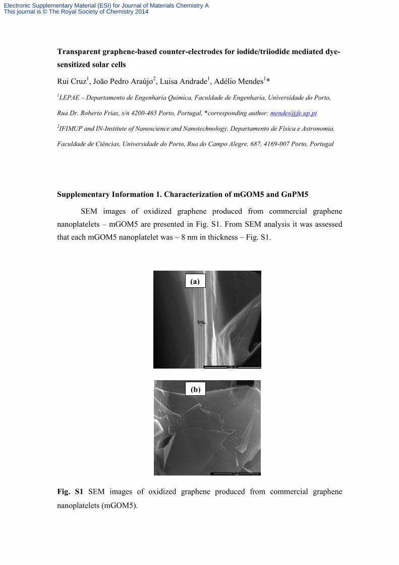
SEM images of oxidized graphene produced from commercial graphene nanoplatelets – mGOM5 are presented in Fig. S1. From SEM analysis it was assessed that each mGOM5 nanoplatelet was ~ 8 nm in thickness – Fig. S1.
Fig. S1 SEM images of oxidized graphene produced from commercial graphene
Supplementary Information 2. Preparation and characterization of the structured mGOM5/Ni films
The developed counter-electrode (CE) based on structured oxidized commercial graphene nanoplatelets and nickel nanoparticles was prepared in three steps. First, a small amount of very small nickel nanoparticles (FTO/Ni) were deposited onto FTO-covered glass by electrophoretic deposition (EDP) – load ca. 0.02 C. This deposition technique is widely used in industry since it has the advantage of being an automated and high throughput process1,2. Second, an aqueous or ethanolic dispersion of oxidized commercial graphene nanoplatelets, mGOM5, were sprayed onto the FTO/Ni substrate with a very small load (~5 – 15 µg∙cm-2). The mGOM5 load used in the different depositions was assessed from the transmittance at 550 nm, τ550nm. Depositions were carried out such that the mGOM5 films had transmittance at 550 nm above 80 %. Afterwards, the GO based CE was annealed under an inert atmosphere (nitrogen). The CE fabricated with mGOM5 and the FTO/Ni substrate is hereafter coded as mGOM5/Ni.
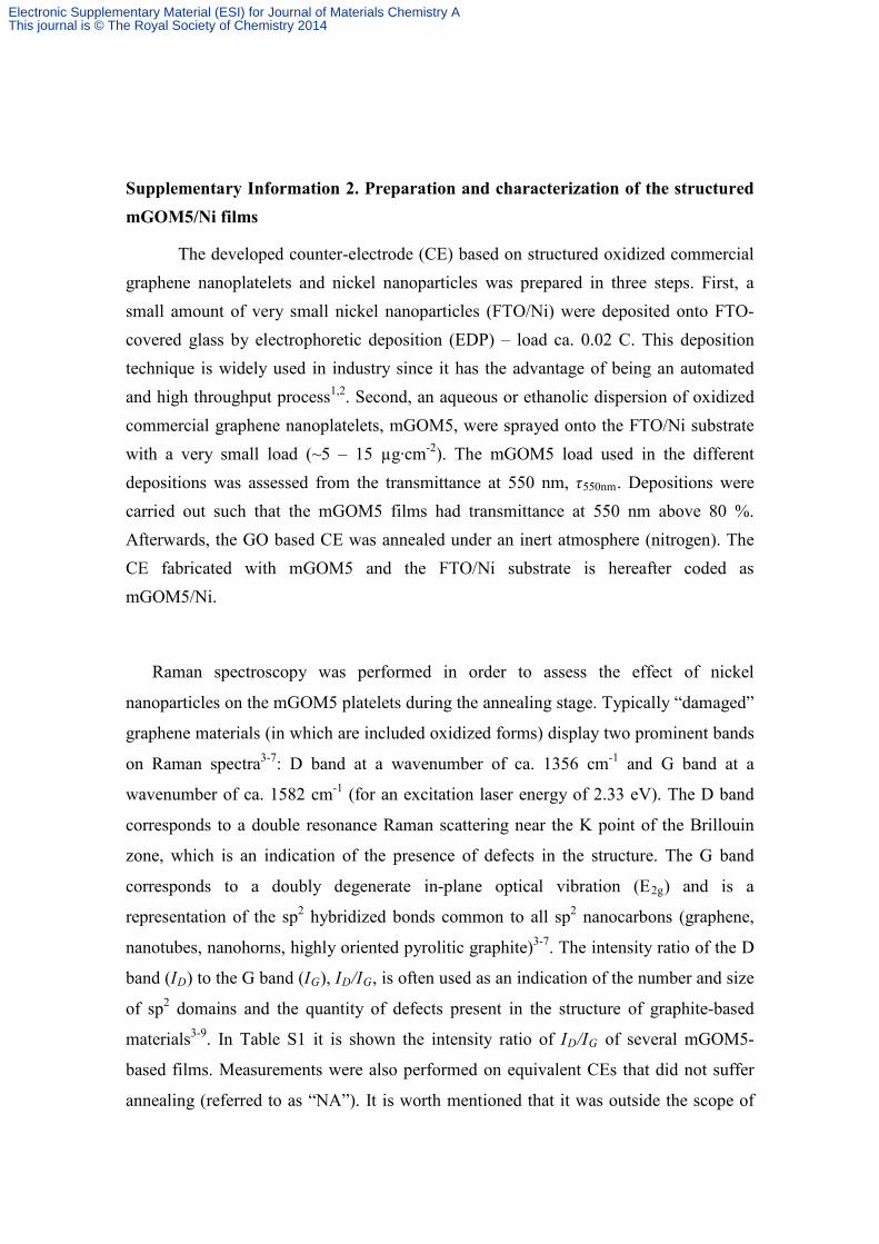
Raman spectroscopy was performed in order to assess the effect of nickel
nanoparticles on the mGOM5 platelets during the annealing stage. Typically “damaged”
graphene materials (in which are included oxidized forms) display two prominent bands
on Raman spectra3-7: D band at a wavenumber of ca. 1356 cm-1 and G band at a
wavenumber of ca. 1582 cm-1 (for an excitation laser energy of 2.33 eV). The D band
corresponds to a double resonance Raman scattering near the K point of the Brillouin
zone, which is an indication of the presence of defects in the structure. The G band
corresponds to a doubly degenerate in-plane optical vibration (E2g) and is a
representation of the sp2 hybridized bonds common to all sp2 nanocarbons (graphene,
nanotubes, nanohorns, highly oriented pyrolitic graphite)3-7. The intensity ratio of the D
band (ID) to the G band (IG), ID/IG, is often used as an indication of the number and size
of sp2 domains and the quantity of defects present in the structure of graphite-based
materials3-9. In Table S1 it is shown the intensity ratio of ID/IG of several mGOM5-
based films. Measurements were also performed on equivalent CEs that did not suffer
annealing (referred to as “NA”). It is worth mentioned that it was outside the scope of
Supplementary Information 3. Analysis of dye-sensitized solar cells
The I-V characteristics of all fabricated dye-sensitized solar cells (DSCs) were obtained applying an external potential bias and measuring the generated photocurrent. The photovoltaic parameters (short-circuit current density, Jsc; open-circuit voltage, Voc; fill factor, FF) were extracted from the I-V curve and used to calculate the efficiency, η:
100x S
SCOC
IFFJV
=η (1)
where IS is the intensity of the incident light.
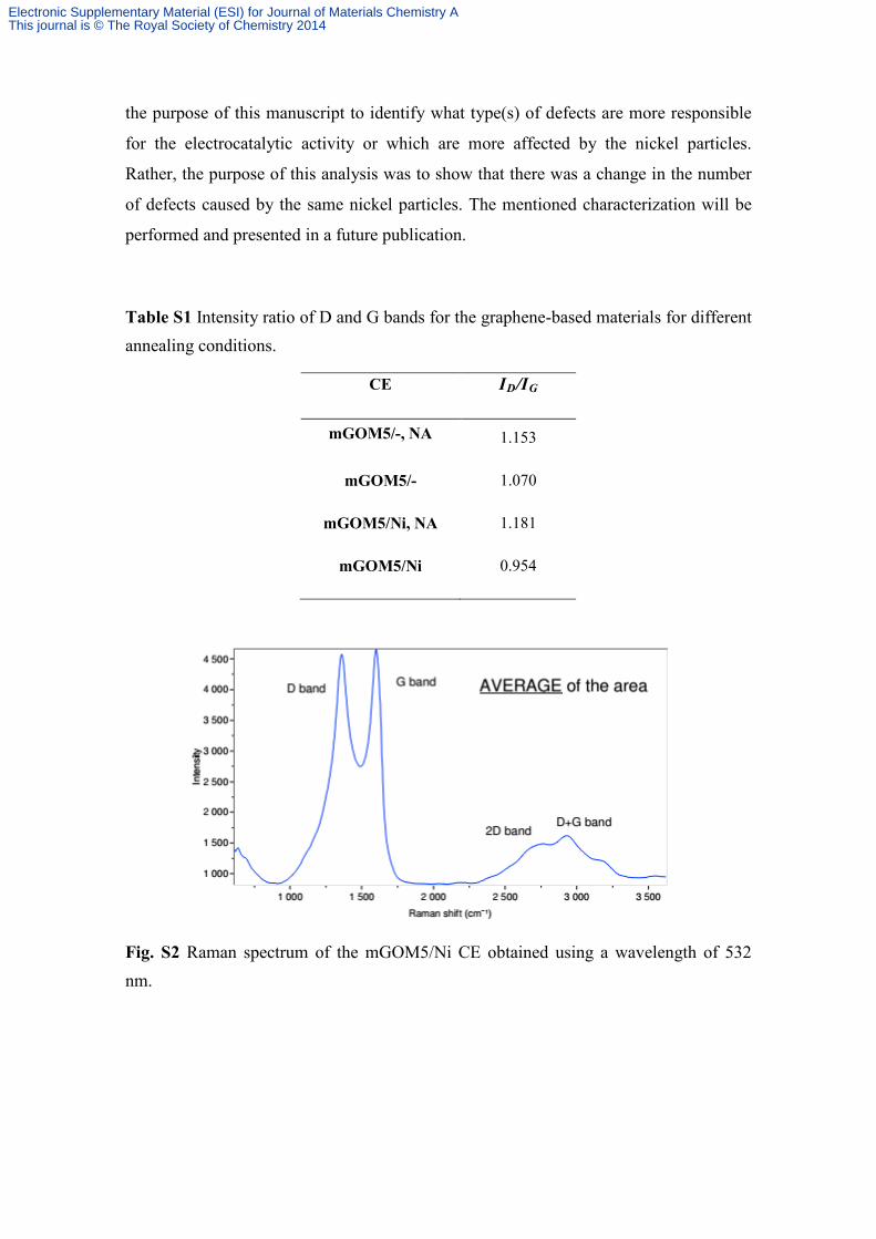
Fig. S3 Pictures of DSCs assembled with CEs of mGOM5, mGOM5/Ni and Pt.
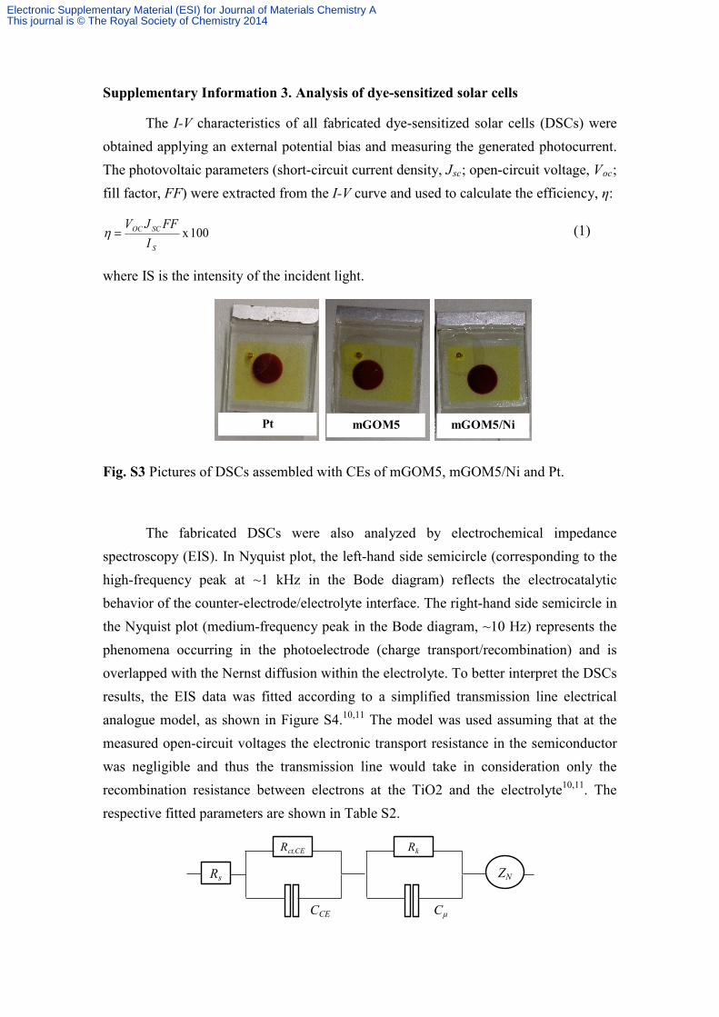
The fabricated DSCs were also analyzed by electrochemical impedance spectroscopy (EIS). In Nyquist plot, the left-hand side semicircle (corresponding to the high-frequency peak at ~1 kHz in the Bode diagram) reflects the electrocatalytic behavior of the counter-electrode/electrolyte interface. The right-hand side semicircle in the Nyquist plot (medium-frequency peak in the Bode diagram, ~10 Hz) represents the phenomena occurring in the photoelectrode (charge transport/recombination) and is overlapped with the Nernst diffusion within the electrolyte. To better interpret the DSCs results, the EIS data was fitted according to a simplified transmission line electrical analogue model, as shown in Figure S4.10,11 The model was used assuming that at the measured open-circuit voltages the electronic transport resistance in the semiconductor was negligible and thus the transmission line would take in consideration only the recombination resistance between electrons at the TiO2 and the electrolyte10,11. The respective fitted parameters are shown in Table S2.
Fig. S4 Electrical analogue used for fitting the electrochemical impedance spectra data of DSCs. ZView software (Scribner Associates Inc.) was used to process the EIS data.
Table S2 EIS fitted parameters of DSCs assembled with the mGOM5/Ni and Pt CEs[a]. Between parentheses is mentioned the solvent used for dispersing the mGOM5/Ni platelets.
CE Rs (Ω) Rs (Ω cm2) Rct,CE (Ω cm2)
Pt 13.6±0.6 5.27±0.2 5.34±0.2
mGOM5/Ni (water) 15.1±0.3 5.81±0.4 2.76±0.6
mGOM5/Ni (ethanol) 14.0±0.4 5.37±0.3 2.30±0.3
[a] Rs – series resistance; Rct – charge transfer resistance.
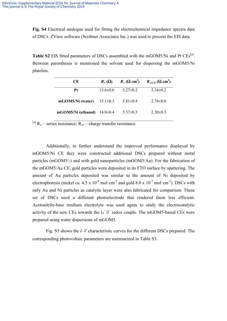
Additionally, to further understand the improved performance displayed by mGOM5/Ni CE they were constructed additional DSCs prepared without metal particles (mGOM5/-) and with gold nanoparticles (mGOM5/Au). For the fabrication of the mGOM5/Au CE, gold particles were deposited in its FTO surface by sputtering. The amount of Au particles deposited was similar to the amount of Ni deposited by electrophoresis (nickel ca. 4.5 x 10⁻⁸ mol·cm-2 and gold 8.0 x 10⁻⁷ mol·cm-2). DSCs with only Au and Ni particles as catalytic layer were also fabricated for comparison. These set of DSCs used a different photoelectrode that rendered them less efficient. Acetonitrile-base medium electrolyte was used again to study the electrocatalytic activity of the new CEs towards the I3
−/I− redox couple. The mGOM5-based CEs were prepared using water dispersions of mGOM5.
Fig. S5 shows the I–V characteristic curves for the different DSCs prepared. The
corresponding photovoltaic parameters are summarized in Table S3.
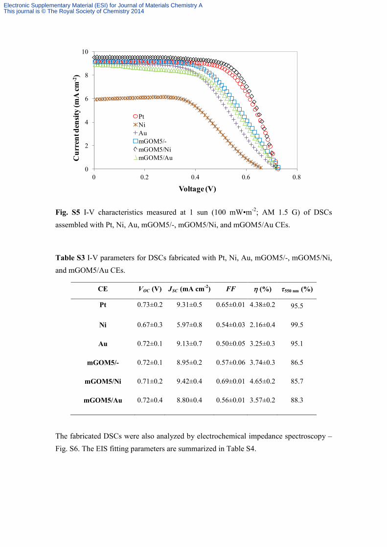
Fig. S6 Electrochemical impedance spectroscopy of DSCs assembled with Pt, Ni, Au, mGOM5/-, mGOM5/Ni, and mGOM5/Au CEs: (a) Nyquist diagrams; (b) Bode diagrams. Measurements carried out in the dark under a bias corresponding to the DSC’s open-circuit voltage (0.7 V). Symbols represent the experimental data and solid lines represent the model fitting. On the insets of the Nyquist diagrams are represented the close-up of the semicircle corresponding to the CE resistance.
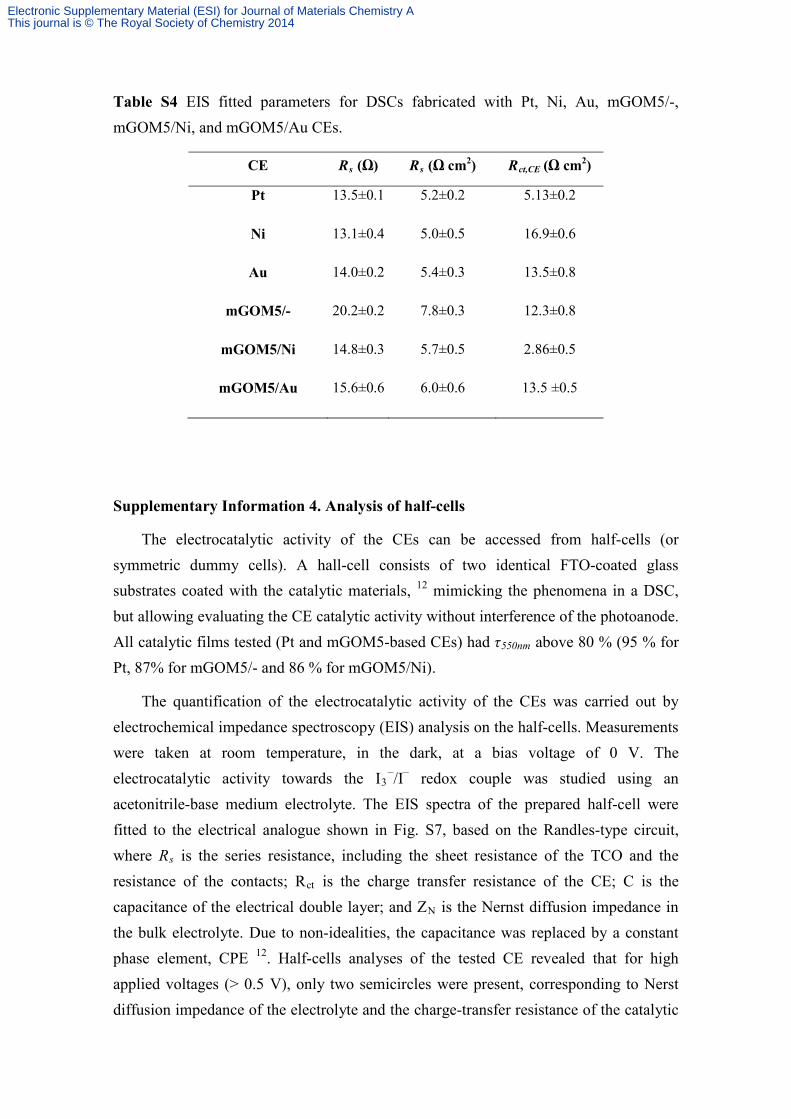
Table S4 EIS fitted parameters for DSCs fabricated with Pt, Ni, Au, mGOM5/-, mGOM5/Ni, and mGOM5/Au CEs.
CE Rs (Ω) Rs (Ω cm2) Rct,CE (Ω cm2)
Pt 13.5±0.1 5.2±0.2 5.13±0.2
Ni 13.1±0.4 5.0±0.5 16.9±0.6
Au 14.0±0.2 5.4±0.3 13.5±0.8
mGOM5/- 20.2±0.2 7.8±0.3 12.3±0.8
mGOM5/Ni 14.8±0.3 5.7±0.5 2.86±0.5
mGOM5/Au 15.6±0.6 6.0±0.6 13.5 ±0.5
Supplementary Information 4. Analysis of half-cells
The electrocatalytic activity of the CEs can be accessed from half-cells (or symmetric dummy cells). A hall-cell consists of two identical FTO-coated glass substrates coated with the catalytic materials, 12 mimicking the phenomena in a DSC, but allowing evaluating the CE catalytic activity without interference of the photoanode. All catalytic films tested (Pt and mGOM5-based CEs) had τ550nm above 80 % (95 % for Pt, 87% for mGOM5/- and 86 % for mGOM5/Ni).
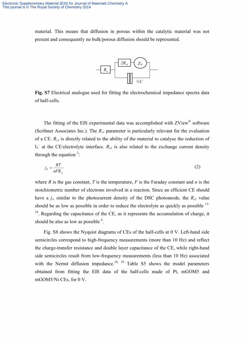
The quantification of the electrocatalytic activity of the CEs was carried out by electrochemical impedance spectroscopy (EIS) analysis on the half-cells. Measurements were taken at room temperature, in the dark, at a bias voltage of 0 V. The electrocatalytic activity towards the I3
−/I− redox couple was studied using an acetonitrile-base medium electrolyte. The EIS spectra of the prepared half-cell were fitted to the electrical analogue shown in Fig. S7, based on the Randles-type circuit, where Rs is the series resistance, including the sheet resistance of the TCO and the resistance of the contacts; Rct is the charge transfer resistance of the CE; C is the capacitance of the electrical double layer; and ZN is the Nernst diffusion impedance in the bulk electrolyte. Due to non-idealities, the capacitance was replaced by a constant phase element, CPE 12. Half-cells analyses of the tested CE revealed that for high applied voltages (> 0.5 V), only two semicircles were present, corresponding to Nerst diffusion impedance of the electrolyte and the charge-transfer resistance of the catalytic
material. This means that diffusion in porous within the catalytic material was not present and consequently no bulk/porous diffusion should be represented.
Fig. S7 Electrical analogue used for fitting the electrochemical impedance spectra data of half-cells.
The fitting of the EIS experimental data was accomplished with ZView® software (Scribner Associates Inc.). The Rct parameter is particularly relevant for the evaluation of a CE. Rct is directly related to the ability of the material to catalyse the reduction of I3
- at the CE/electrolyte interface. Rct is also related to the exchange current density through the equation 2:
ctnFRRTj =0
(2)
where R is the gas constant, T is the temperature, F is the Faraday constant and n is the stoichiometric number of electrons involved in a reaction. Since an efficient CE should have a jo similar to the photocurrent density of the DSC photoanode, the Rct value should be as low as possible in order to reduce the electrolyte as quickly as possible 13-
16. Regarding the capacitance of the CE, as it represents the accumulation of charge, it should be also as low as possible 6.
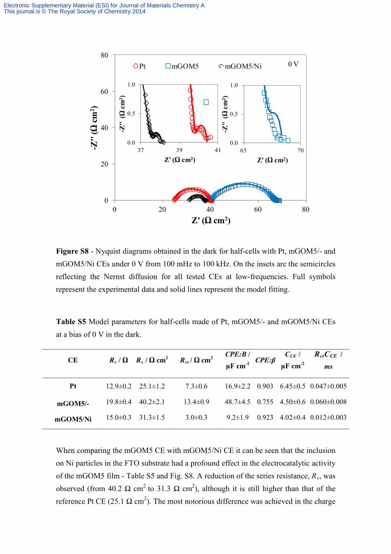
Fig. S8 shows the Nyquist diagrams of CEs of the half-cells at 0 V. Left-hand side semicircles correspond to high-frequency measurements (more than 10 Hz) and reflect the charge-transfer resistance and double layer capacitance of the CE, while right-hand side semicircles result from low-frequency measurements (less than 10 Hz) associated with the Nernst diffusion impedance.18, 19 Table S5 shows the model parameters obtained from fitting the EIS data of the half-cells made of Pt, mGOM5 and mGOM5/Ni CEs, for 0 V.
Figure S8 - Nyquist diagrams obtained in the dark for half-cells with Pt, mGOM5/- and mGOM5/Ni CEs under 0 V from 100 mHz to 100 kHz. On the insets are the semicircles reflecting the Nernst diffusion for all tested CEs at low-frequencies. Full symbols represent the experimental data and solid lines represent the model fitting.
Table S5 Model parameters for half-cells made of Pt, mGOM5/- and mGOM5/Ni CEs at a bias of 0 V in the dark.
When comparing the mGOM5 CE with mGOM5/Ni CE it can be seen that the inclusion on Ni particles in the FTO substrate had a profound effect in the electrocatalytic activity of the mGOM5 film - Table S5 and Fig. S8. A reduction of the series resistance, Rs, was observed (from 40.2 Ω cm2 to 31.3 Ω cm2), although it is still higher than that of the reference Pt CE (25.1 Ω cm2). The most notorious difference was achieved in the charge
transfer resistance of the mGOM5/Ni CE (3.0 Ω cm2), which greatly dropped below the value of Rct of the Pt CE (7.3 Ω cm2). Both CEs had Rct values below 10 Ω cm2, the threshold recommended for high performance cells 12. The mGOM5/Ni CE also displays a lower capacitance than the Pt CE (9.2 µF cm-2 vs. 16.9 µF cm-2, respectively). This means that less charge is accumulated at the mGOM5/Ni CE/electrolyte interface during the reduction of I3
− ions, presumably due to its better catalytic nature. Considering that the graphene-based CEs had roughly the same thickness (because they had similar transmittances) and therefore the same available surface area for catalysis, the fact that the mGOM5 CE showed a high capacitance and high Rct seems to indicate that Ni particles might played a role for the increased electrocatalytic activity.
For better quantitative comparison of such thin films, the product RctCCE was used as a figure of merit for their catalytic activity. For that it was assumed that the area-specific capacitance of the CEs only depends on the capacitance of the Helmholtz layer double layer per microscopic surface area, which if similar in carbon materials of metallic nature.14 As the capacitance had been previously replaced by a constant phase element for fitting the Nyquist curves, it was necessary to calculate the overall capacitance, CCE 20:
( )ct
CPEctCE R
BCPERCβ:
1:
= (3)
The results in Table S5 show that the mGOM5/Ni CE has a RctCCE of 0.012 ms, much lower than the one obtained for the Pt CE – 0.047 ms. The mGOM5 CE exhibit the worst RctCCE value (0.06 ms). These results further confirm the higher catalytic activity yield by the mGOM5/Ni CE.
1 Wu, Z.-S. et al. Field Emission of Single-Layer Graphene Films Prepared by Electrophoretic Deposition. Advanced Materials 21, 1756-1760, doi:10.1002/adma.200802560 (2009).
2 Van der Biest, O. O. & Vandeperre, L. J. Electrophoretic deposition of materials. Annual Review of Materials Science 29, 327-352, doi:doi:10.1146/annurev.matsci.29.1.327 (1999).
3 Dresselhaus, M. S., Jorio, A., Hofmann, M., Dresselhaus, G. & Saito, R. Perspectives on Carbon Nanotubes and Graphene Raman Spectroscopy. Nano Letters 10, 751-758, doi:10.1021/nl904286r (2010).
4 Charlier, J. C., Eklund, P. C., Zhu, J. & Ferrari, A. C. in Carbon Nanotubes Vol. 111 Topics in Applied Physics Ch. 21, 673-709 (Springer Berlin Heidelberg, 2008).
5 Ferrari, A. C. et al. Raman Spectrum of Graphene and Graphene Layers. Physical Review Letters 97, 187401 (2006).
6 Pimenta, M. A. et al. Studying disorder in graphite-based systems by Raman spectroscopy. Phys. Chem. Chem. Phys. 9, 1276-1290 (2007).
7 Dikin, D. A. et al. Preparation and characterization of graphene oxide paper. Nature 448, 457-460, doi:doi:10.1038/nature06016 (2007).
8 Zhan, D. et al. Electronic structure of graphite oxide and thermally reduced graphite oxide. Carbon 49, 1362-1366, doi:DOI: 10.1016/j.carbon.2010.12.002 (2011).
9 Wang, S. J., Geng, Y., Zheng, Q. & Kim, J.-K. Fabrication of highly conducting and transparent graphene films. Carbon 48, 1815-1823, doi:10.1016/j.carbon.2010.01.027 (2010).
10 Kern, R., Sastrawan, R., Ferber, J., Stangl, R. & Luther, J. Modeling and interpretation of electrical impedance spectra of dye solar cells operated under open-circuit conditions. Electrochimica Acta 47, 4213-4225 (2002).
11 Andrade, L., Sousa, J., Ribeiro, H. A. & Mendes, A. Phenomenological modeling of dye-sensitized solar cells under transient conditions. Solar Energy 85, 781-793, doi:10.1016/j.solener.2011.01.014 (2011).
12 A. Hauch and A. Georg, Electrochimica Acta, 2001, 46, 3457-3466.
13 A. Hagfeldt, G. Boschloo, L. Sun, L. Kloo and H. Pettersson, Chemical Reviews, 2010, 110, 6595-6663.
14 K. Aitola, J. Halme, N. Halonen, A. Kaskela, M. Toivola, A. G. Nasibulin, K. Kordás, G. Tóth, E. I. Kauppinen and P. D. Lund, Thin Solid Films, 2011, 519, 8125-8134.
15 L. Kavan, J.-H. Yum and M. Grätzel, Nano Letters, 2011, 11, 5501-5506. 16 N. Papageorgiou, W. Maier and M. Grätzel, Journal of The Electrochemical
Society, 1997, 144, 876-884. 17 J. Velten, A. J. Mozer, D. Li, D. Officer, G. Wallace, R. Baughman and A.
Zakhidov, Nanotechnology, 2012, 23. 18 L. Kavan, J. H. Yum and M. Grätzel, ACS Nano, 2010, 5, 165-172. 19 J. D. Roy-Mayhew, D. J. Bozym, C. Punckt and I. A. Aksay, ACS Nano, 2010,
4, 6203-6211. 20 J. Halme, P. Vahermaa, K. Miettunen and P. Lund, Advanced Materials, 2010,
22, E210-E234.
Fruitful help from Dr. Célia Sousa, Arlete Apolinário and João Azevedo regarding electrophoresis and sputtering deposition is acknowledged. The authors would also like to acknowledge José Maçaira and Fernando Ribeiro. Vincent Larat and Romain Bruder are also acknowledged for assistance with the Ramana analysis.