Graphene Optical Switch Based on Charge TransferPlasmons
Arash Ahmadivand,* Burak Gerislioglu, and Nezih Pala
In the past decade, dynamic, tunable, compact, and fast plasmonic switcheswith high modulation depth (MD) and low losses have been developedsuccessfully for various practical applications. Here, using a simpleplasmonic dimer consisting of a pair of metallic nanodisks bridged to eachother with a graphene monolayer, we develop a highly tunable plasmonicswitch for telecommunication applications. We have shown that having activecontrol on the photoconductivity of graphene sheet through electrical biasallows for transition of charges across the atomically thin bridge, giving riseto formation of charge transfer plasmon (CTP) modes. Such an interplaybetween semiconducting and semi-metallic states of the graphene sublayerleads to direct control of the excited CTPs. By tuning the peak of CTP at theglobal telecommunication band (λ¼ 1550 nm), we designed an integrated,fast, and functional optoelectronic nanoswitch with high MD up to �98%and negligible losses. This study presents a promising approach to designtunable, high-quality, integrated optoelectronic switches for next-generationadvanced nanophotonic applications.
Quantum plasmonics has witnessed growing progress due toproviding exquisite features that cannot be achieved simply byclassical concept of optical physics.[1–3] Several strategies havebeen proposed to investigate the spectral features of plasmonicstructures in atomic levels. Bringing a pair of metallic nano-particles close to each other and reducing the gap between themto subnanometer dimensions (below <1 nm) has been acknowl-edged as a successful technique to realize quantum plasmonicsby tunneling of photoexcited electrons across the atomicopening.[1,4,5] The size of the gap determines the type ofquantum tunneling principle as a direct[1,6] or indirect (known asFowler–Nordheim tunneling)[7] tunneling. One interestingresult of molecular tunneling of charges is the excitation ofadditional plasmonic modes at lower energies which is apartfrom the classically hybridized plasmons (i.e., dipolar, quad-rupolar, etc.), known as charge transfer plasmon (CTP).[1,4–7] TheCTPmode is a unique and direct result of a quantummechanicaleffect supported by subwavelength nanoparticles, inspired fordevelopment of innovative quantum devices. However, despite
A. Ahmadivand, B. Gerislioglu, Dr. N. PalaDepartment of Electrical and Computer Engineering, FloridaInternational University, 10555W Flagler St, Miami, FL 33174, USAE-mail: [email protected]
Arash Ahmadivand and Burak Gerislioglu contributed equally to thiswork.
the advanced nanofabrication technologies,accessing to CTP modes using nanostruc-tures with atomic gaps is challenging,costly, and needs for complex nanofabri-cation procedures as well as complicatedquantum model computations.
Recently, alternative and affordablemethods have been proposed and analyzedtheoretically and experimentally to exciteCTPs in the near-infrared (NIR),[8,9] andterahertz (THz) spectra,[10] via direct trans-fer of charges between subwavelengthplasmonic objects across a conductivebridge. In both tunneling and directshuttling of electrons, having an activecontrol over CTPs is limited and can becontrolled partially by varying the intensityof the incident radiation or morphologicalvariations.[7,11,12] Excitation of CTPs in acontrollable and functional fashion wouldallow for designing ultrafast and efficienton/off (set/reset) devices such as telecom-munication routers, single molecule sen-
sors, and advanced optoelectronic devices.[3,5,13] Recently, byusing a metallodielectric structure, we showed that CTPresonances can be effectively controlled by varying theconductance of the junction between linked nanodisks.[14] Thisunique feature was realized by using a phase-changing material(Ge2Sb2Te5) as a nanobridge that allows and controls the chargetransfer between the metallic nanoparticles, via conductivityvariations due to external heat stimuli. However, switchingbetween amorphous and crystalline phases of a nonvolatilematerial needs for applying Joule heating at high temperatures(0477 �C).[15,16] This hinders broad usage of phase-changingmaterial-based controllable CTPs in integrated nanophotonicsystems that are sensitive to high temperatures.
Recently, Frenzel et al.[17] have shown that the photoconduc-tivity of a monolayer graphene sheet can be controlled efficientlyby applying bias via tuning the generated carrier density. Such afeature was achieved by modeling the electronic properties ofgraphene in terms of massless Dirac fermions.[17–20] Besides,graphene has been successfully demonstrated as a promisingsubstance for plasmonic purposes due to its substantial opticalpower absorption along a wide range of spectrum,[21,22] and alsoits semi-metallic behavior with an optical conductivity as afunction of quantum conductance as[18–23]: σ¼ πe2/2h, where e isthe elementary charge and h is the Planck’s constant. Similar tothe nanoplasmonic components, the spectral response ofgraphene single-monolayer can be understood by Drudeabsorption model for a wide range of carrier densities.[23,24]
This temperature-independent model for free carrier photocon-ductivity with parabolic dispersion in a 2D monolayer can bewritten as a function of frequency[25–27]: σ(ω)¼ ne2/m(Γ-iω),where m is the electron mass and Γ is the transport scatteringrate. It should be underlined that in the presented work,graphene monolayer with local conductivity is presented withthe ability to transfer charges with lower decay rate and higherlifetime of charges.[22]
In this work, we report a systematic study of a pair of metallicnanoparticles connected with a gate tunable graphene sublayerto control the transfer of photoinduced electrons across theatomic junction effectively via tuning the corresponding carrierdensity. Using full wave electromagnetic numerical and finite-element multiphysics simulation studies, we show that theoptically excited charges supported by proximal metallic nano-particles can be tuned and guided by electrically varying theconductivity of the graphene sublayer. The achieved resultsverified that at the semiconducting regime of graphenecapacitive coupling between the dipolar modes on the nanodisksbecomes dominant and leads to formation of a distinguisheddipolar peak of extinction in the visible region. Then, by applyinggate bias to the system, graphene sublayer acts as a semi-metallicconductive layer, in which a new tunable peak appears at the NIRspectra, correlating with the CTPmode in addition to the dipolarpeak in the visible domain. Both longer lifetime and betterconfinement of the optically driven plasmons in n-dopedgraphene layer lead to efficient manipulation of charges inthe system by varying the doping level through electrostaticgating approach.[28,29] Using the interplay between photoexcitedcharges at both semiconducting and semi-metallic regimes, weadjusted the peak of the CTP mode at the global telecommuni-cation wavelength (1550 nm) to develop a tunable and fastgraphene-plasmonic nanoswitch.
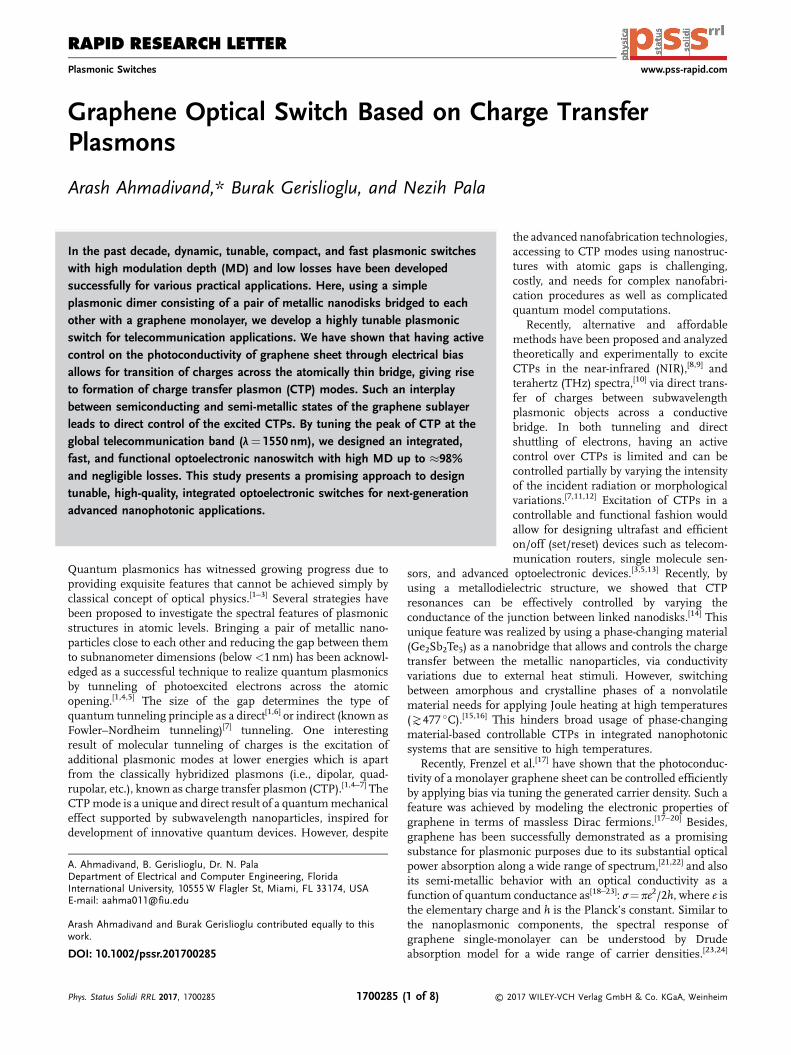
Figure 1a and b illustrate the 3D schematic and top-viewimage, respectively (not to scale), of the proposed plasmonicswitching device composed of a pair of gold nanodisks connectedwith a single-layered graphene sublayer with back-gated voltage(Vg) as well as source and drain contacts. We used theexperimentally dielectric function determined by Johnson–Christy[30] for the gold nanoparticles and relative permittivity of�2.1 for the glass (SiO2) substrate, measured by Palik.[31] It
Figure 1. a) An artistic rendering of the proposed device composed of gold nacorresponding geometrical parameters. c) Electrical transport characteristic cthe proposed graphene-plasmonic platform. The diameter of nanodisks isthickness is t¼ 45 nm for both. The distance between source–drain electro
Phys. Status Solidi RRL 2017, 1700285 1700285 (
should be noted that the graphenemonolayer is in ohmic contactwith the source and drain electrodes in both sides. It should beunderlined that the thickness of the graphenemonolayer is set to0.35 nm and for simplicity the thickness of the plasmonicnanodimer is set to 45 nm due to having negligible influence onthe CTP intensity.
For the absence of gold nanodisks, the graphene monolayerwith carrier density close to the neutrality point acts similar tothe conventional semiconductors, and we expect generation ofelectron–hole pairs under light exposure and significantabsorption of incident electromagnetic wave at thispoint.[17,32–34] Conversely, when the charge density in grapheneis high, variations in the charge distribution are close to theFermi level.[17,21,35,36] In this regime, graphene sheet behaves asa conductive substance similar to the metals. However, in thepresence of metallic nanoparticles in direct contact with thegraphene layer, injection of hot-electrons into the graphene layerplays fundamental role in determining the spectral andelectronic response of the system. In the dimer nanoantennacase, the photoinduced hot-electrons generated in the metallicdisks are injected into the graphene sheet, resulting in n-typedoped graphene monolayer, possessing minor role in thedoping type.[35,37] As a major and critical parameter, the dopingconcentration of graphene can be electrically tuned allowing forswitching between semiconductor and semi-metallic regimes viathe control over its photoconductivity. Figure 1c exhibits theresistance (R) variations for the plasmonic dimer nanoassemblyon the graphene sublayer as a function of back-gate voltageunder incident beam illumination. This characteristic profileindicates the Dirac point for graphene-plasmonic regime. In thegraphene-plasmonic limit, the Dirac point is reached at the gatevoltage around �28V, while the applied source-drain (VDS) biasin both analyses was set to 1mV.[38,39] Using this approach,the carrier concentration qualitatively can be tuned around�2� 1013 cm�2. The shift in the Dirac point for the graphene-plasmonic case can be explained by considering the variations inthe graphene work function due to direct contact with goldnanoparticles. Comparing the graphene sheet without and withcontact with metallic structures, for the latter case, there is asteady inclination of the Dirac energy level along the horizontaldirection close to the contact edge due to work function
nodisks and graphene monolayer. b) A top-view of the device showing theurves as resistance variations (R) as a function of back-gate voltage (Vg) ford¼ 125 nm and the offset space between them is La¼ 100 nm while thedes is Lg¼ 500 nm and the width of graphene sublayer is W¼ 160 nm.
difference between illuminated graphene sheet and the 2D layerbeneath the metallic nanoparticles.[40–42]
Figure 2a and b compare the extinction spectra for the absence(graphene sublayer) and presence of plasmonic dimer antennaon the graphenemonolayer. The electromagnetic response of thenanosystem is obtained for the n-doped graphene with the Fermienergy of EF¼ 0.61 eV, taken from experimental reports by Fanget al.[39,43,44] for graphene disks and rings in hybridized regime(EF¼ �hvF(πn)
1/2, where, vF¼ 106m s�1, and n is the chargecarrier density).[44] Thus for the applied gate bias and incidentbeam, highly doped graphene sheet shows substantiallyconductive behavior and a distinct dipolar peak appears atE¼ 0.44 eV, consistent with atomistic analysis achieved byrandom-phase approximation (RPA) for graphene plasmonics inprevious studies.[45,46] The inset shows the local E-field map forthe dipolar plasmon resonance excitation in a graphene layer. Onthe other hand, for the presence of nanodisks in direct contactwith highly doped graphene sublayer, we observed formation ofdistinguished resonant peaks at E¼ 2.78 and 0.81 eV, correlatingwith the dipolar and CTPmodes, respectively. The large gap areabetween proximal nanodisks prevents strong near-field hybrid-ization of plasmons. Here graphene layer acts as a conductivepathway to transfer the charges between the neighbor nanodisks,therefore, opposite charges accumulate at both sides, giving riseto formation of a CTP mode at lower energies. The mechanismof the transport of photoexcited charges can be better understoodby analyzing the behavior of graphene at high doping (EF>ω).[22]
It is well accepted that using Drude model, homogenous
Figure 2. a) Extinction cross-section of a highly doped to EF¼ 0.61 eV (n-tyT¼ 300 K. The inset is the E-field intensity map for the dipolar mode. b) Egraphene nanoribbon bridge, supporting dipolar (II), CTP (III), quadrupolar (the plasmon resonance excitation and distribution across the device for dipolfeature and dipolar modes.
Phys. Status Solidi RRL 2017, 1700285 1700285 (
graphene with plasmonic properties supports propagation ofphotoinduced electrons with the wave vector of[21,28,29,46,47]:
ksp � �h2
e2EF
!ω eþ 1ð Þ ωþ i=τð Þð Þ ð1Þ
where τ is the finite relaxation time, and e is the relativepermittivity. Therefore, due to large photoconductivity ofgraphene, we expect longer relaxation time compared to noblemetals and lower dissipative losses similar to the graphenenanoribbon waveguides with plasmonic properties.[29] In otherwords, graphene monolayer underneath the metallic particlesacts as the charge transfer channel between the metallic (gold)and oxide (SiO2) interfaces, has been previously confirmed andmeasured by Kelvin probe force microscopy.[48,49] On the otherhand, two distinct resonant peaks are induced at 0.43 and 0.31 eVcorrelating with the quadrupolar and dipolar modes supportedby conductive graphene sublayer junction between nanodisks.Here, the quadrupolar mode appeared due to intense doping ofgraphene monolayer simultaneously by the gate bias andinjected electrons to the graphene sheet, enhancing theplasmonic properties of the layer. Moreover, variations in thedoping properties of graphene lead to a red-shift in the positionof the dipolar peak to the lower energies. The charge distributionmaps for the graphene plasmonic regime at different modes areillustrated in Figure 2c. Figure 2d demonstrated the local E-fieldintensity for the charge distribution across the dimer for both
pe) graphene nanoribbon under optical excitation at room-temperaturextinction spectra of plasmonic nanodimer antenna on the highly dopedIV), and dipolar (V) moments. c) The local |E|-field intensity snapshots fore (II) and CTP (III) modes. d) The charge density plots for the CTP spectral
CTP and dipole modes. These results strongly confirm the claimthat at the CTP position the negative and positive charges areconcentrated at the opposite sides due to direct transport ofcharges through the channel, while in the dipolar mode energy,the capacitive coupling becomes dominant due to weakinterference of energetic dipolar modes from each nanodisk.
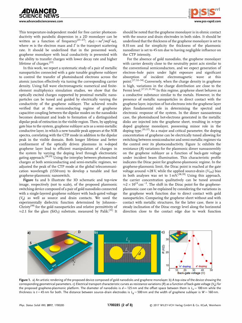
Here, the optically excited CTP can be simply tuned at thedesired energy or wavelength by varying the conductivity of theatomic sublayer. To this end, we carried out specific geometricalvariations for the analyzed plasmonic device. Figure 3a and billustrate the behavior of both dipolar and CTPmodes supportedby themetallic nanodisks. One should note that we neglected thebehavior of dipolar and multipolar modes at the low energiessupported with graphene sheet and the Fermi level is fixed toEF¼ 0.61 eV. As shown in Figure 3a, increasing the edge-to-edgedistance (La) between nanoparticles from 50 to 120 nm gives riseto dramatic red-shift in the position of CTP mode to the lowerenergies, while the diameter of the disks is fixed to d¼ 125 nm.This can be better understood by analyzing the conductance ofthe graphene junction. It is shown that increasing the length ofthe conductive bridge between neighbor nanoparticles causesincrease in electron travel time between the nanoparticles as wellas dramatic decay of plasmons due to longer travel area.[8,14,29]
Figure 3. Normalized extinction spectra for a) interparticle distance (50variations, respectively. The doping of graphene is n-type Fermi level energ
Phys. Status Solidi RRL 2017, 1700285 1700285 (
Therefore, for the highly doped n-type graphene layer, thefrequency-dependent conductance can be written as:G(ω)¼ σ(ω)WT/La, where W, T, and La are the width (fixed to 160 nm),thickness (here set and fixed to 0.35 nm), and the length of thegraphene layer, respectively. The frequency-dependent conduc-tivity of an atomic graphene bridge composed of intraband(Drude model response) and interband transitions (lossy part)has been reported using RPA as below[22,47]:
σðωÞ ¼ e2EF
π�h2i
ωþ i=τ
� �
þ e2
4�hθ �hω� 2EFð Þ þ i
π
�hω� 2EF
�hωþ 2EF
��������
� �: ð2Þ
Consequently, by increasing the length of the pathway, theconductance reduces slightly and delays the shuttle of thephotoexcited charges. Nevertheless, it is noteworthy that due tothe substantial conductivity of highly doped graphene sheet, wedo not expect dramatic shift in the position of CTP peak tothe mid-infrared region (MIR) as it happens in dissipativemetallic and lossy junctions.[8,10,14] On the other hand,increasing the space between proximal disks causes drasticdecay in the amplitude of the dipolar peak at high energies.
nm� La� 120 nm) and b) nanodisks diameters (75 nm� d� 150 nm)y if fixed to EF¼ 0.61 eV.
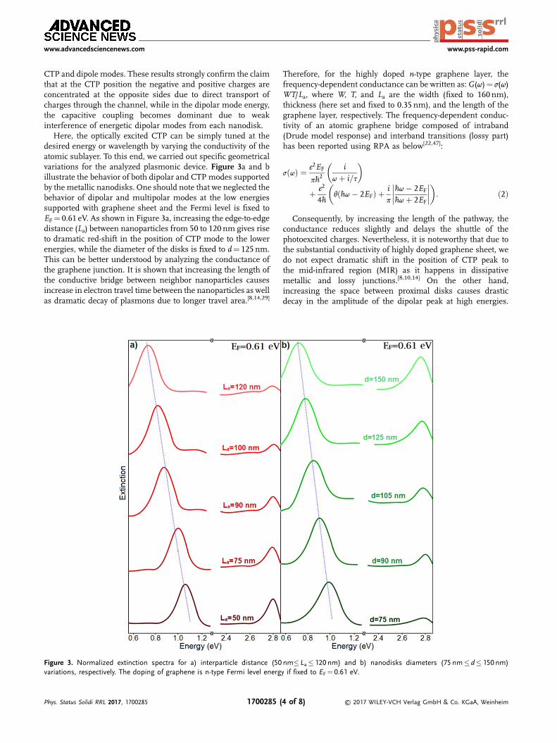
Figure 4. a) Normalized extinction spectra for the “On” and “Off”states of the graphene-plasmonic nanoswitch in the presence andabsence of back-gate voltage. The critical geometrical parameters areLa¼ 100 nm, d¼ 120 nm. The inset is the local E-field map for thedipolar resonance, when the graphene sublayer is in semiconductingregime. b) CTP energy as a function of gate voltage variations (ΔVg).The insets are the extinction diagram for the plasmonic nanoswitch forthe gate voltage variations below the Dirac point and the Q-factor ofCTP peak for the gate voltage variations. c) Numerically quantified MDof the graphene-plasmonic switch as a function of incident photonwavelength with higher resolution under back-gate bias application (atthe Dirac point).
www.advancedsciencenews.com www.pss-rapid.com
Figure 3b represents the spectral response of the analyzed devicefor variations in the diameter (d) of the nanodisks. Keeping thedimer system symmetric, we homogenously increased thediameter from 75 to 150 nm, while the edge-to-edge gap is fixedto La¼ 100 nm. In this limit, by increasing the size of nanodisks,the CTP extreme red-shifts to the lower energies due tosimultaneous increases in both charge separation distance andelectron travel time across the structure. The dipolar peak at highenergies significantly enhanced by increasing the size of disksdue to stronger dipolar interference.
Having tunable CTP modes around the telecommunicationband allows us using the graphene-plasmonic structure as anoptoelectronic nanodevice for NIR optical switching. In thisprocess, tunable conductivity of graphene determines theelectromagnetic response of the structure, and hence itsswitching properties. As previously mentioned, graphene withcarrier density close to neutrality point acts similar to thesemiconductors. Therefore, we expect formation of dipolar peakat high energies (here�2.7 eV) and elimination of CTP peak dueto absence of conductive junction to transfer the charges (Offstate). On the other hand, highly n-doped graphene with semi-metallic behavior shows high conductivity,[50,51] and facilitatestransfer of charges resulting excitation of CTP mode at thetargeted wavelength (On state). Figure 4a exhibits the normal-ized extinction spectra for the proposed device under incidentbeam illumination and varying back-gate bias. Clearly, in theabsence of gate voltage (or low photoconductivity of grapheneclose to the charge neutrality point), the CTP mode disappears,while for the required applied bias and n-doped regime (higherconductivity), a pronounced CTP peak appeared around 0.8 eV(λ� 1.55mm), shown by a dotted line in the plotted spectra. Thedetails for the geometrical sizes are given in the figure caption.The inset is the local E-field map for dipolar resonant mode(�2.7 eV) when the graphene sublayer is in semiconducting orintrinsic regime (Vg Off). The position and energy of CTP peakas a function of back-gate voltage variations (35V�ΔVg� 50V)is shown in Figure 4b. As discussed earlier, the peak of CTPmode is located at 0.8 eV for the applied voltage far away from theDirac point with lower resistance and intense doping ofgraphene sheet (Vg¼ 50V). Continuous reduction in the back-gate voltage leads to a blue-shift in the position of the resonantmode to higher energies due to reaching the intrinsic point andhuge increase in the atomic sheet resistance. The insets inFigure 4b provide more details for destructive results of gate-voltage variations. Here, the extinction spectra reveal how theCTPmode greatly damped forΔVg� 35V (reaching the intrinsiclevel). This originates due to significant reduction in the carrierconcentration (low doping regime) and the conductance of theatomic carbon bridge. The other inset profile demonstrates theQ-factor of CTP mode as a function of gate voltage variations,confirming the drastic decay of CTP mode by reducing the biasvoltage and losing the conductivity of junction. Here, the Q-factor is quantified as the ratio of resonance wavelength to thefull width at half maximum (FWHM). Figure 4c shows the MDof the switch as a function of incident light wavelength. Thisprofile confirms the archived high MD up to 98% at the globaltelecommunication wavelength (C-band) using functional CTPresonant mode. Such a high MD is comparable with and higher
that analogous plasmons inspired graphene-based, molecular,and atomic all-optical and optoelectronic switches.[52–57]
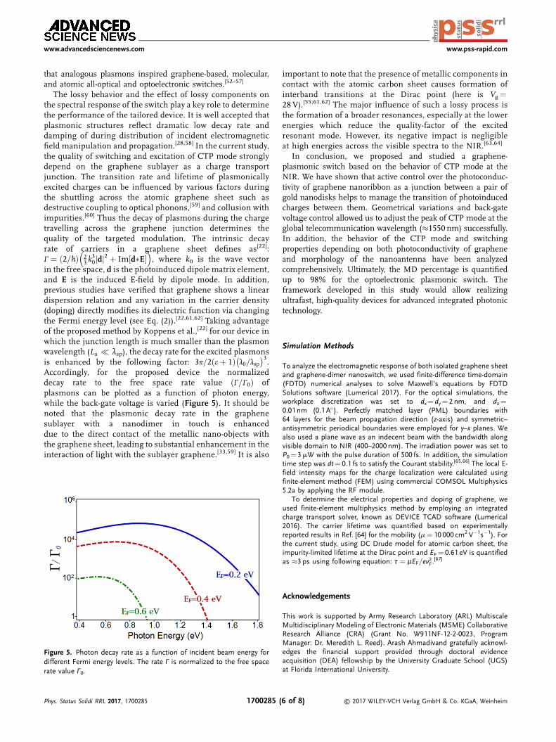
The lossy behavior and the effect of lossy components onthe spectral response of the switch play a key role to determinethe performance of the tailored device. It is well accepted thatplasmonic structures reflect dramatic low decay rate anddamping of during distribution of incident electromagneticfield manipulation and propagation.[28,58] In the current study,the quality of switching and excitation of CTP mode stronglydepend on the graphene sublayer as a charge transportjunction. The transition rate and lifetime of plasmonicallyexcited charges can be influenced by various factors duringthe shuttling across the atomic graphene sheet such asdestructive coupling to optical phonons,[59] and collusion withimpurities.[60] Thus the decay of plasmons during the chargetravelling across the graphene junction determines thequality of the targeted modulation. The intrinsic decayrate of carriers in a graphene sheet defines as[22]:Γ ¼ 2=�hð Þ 2
3 k30 dj j2 þ Im d�E½
� �, where k0 is the wave vector
in the free space, d is the photoinduced dipole matrix element,and E is the induced E-field by dipole mode. In addition,previous studies have verified that graphene shows a lineardispersion relation and any variation in the carrier density(doping) directly modifies its dielectric function via changingthe Fermi energy level (see Eq. (2)).[22,61,62] Taking advantageof the proposed method by Koppens et al.,[22] for our device inwhich the junction length is much smaller than the plasmonwavelength (La λsp), the decay rate for the excited plasmonsis enhanced by the following factor: 3π=2 eþ 1ð Þ λ0=λsp
� �3.
Accordingly, for the proposed device the normalizeddecay rate to the free space rate value Γ=Γ0ð Þ ofplasmons can be plotted as a function of photon energy,while the back-gate voltage is varied (Figure 5). It should benoted that the plasmonic decay rate in the graphenesublayer with a nanodimer in touch is enhanceddue to the direct contact of the metallic nano-objects withthe graphene sheet, leading to substantial enhancement in theinteraction of light with the sublayer graphene.[33,59] It is also
Figure 5. Photon decay rate as a function of incident beam energy fordifferent Fermi energy levels. The rate Γ is normalized to the free spacerate value Γ0.
Phys. Status Solidi RRL 2017, 1700285 1700285 (
important to note that the presence of metallic components incontact with the atomic carbon sheet causes formation ofinterband transitions at the Dirac point (here is Vg¼28 V).[55,61,62] The major influence of such a lossy process isthe formation of a broader resonances, especially at the lowerenergies which reduce the quality-factor of the excitedresonant mode. However, its negative impact is negligibleat high energies across the visible spectra to the NIR.[63,64]
In conclusion, we proposed and studied a graphene-plasmonic switch based on the behavior of CTP mode at theNIR. We have shown that active control over the photoconduc-tivity of graphene nanoribbon as a junction between a pair ofgold nanodisks helps to manage the transition of photoinducedcharges between them. Geometrical variations and back-gatevoltage control allowed us to adjust the peak of CTP mode at theglobal telecommunication wavelength (�1550 nm) successfully.In addition, the behavior of the CTP mode and switchingproperties depending on both photoconductivity of grapheneand morphology of the nanoantenna have been analyzedcomprehensively. Ultimately, the MD percentage is quantifiedup to 98% for the optoelectronic plasmonic switch. Theframework developed in this study would allow realizingultrafast, high-quality devices for advanced integrated photonictechnology.
Simulation Methods
To analyze the electromagnetic response of both isolated graphene sheetand graphene-dimer nanoswitch, we used finite-difference time-domain(FDTD) numerical analyses to solve Maxwell’s equations by FDTDSolutions software (Lumerical 2017). For the optical simulations, theworkplace discretization was set to dx¼ dy¼ 2 nm, and dz¼0.01 nm (0.1 A�). Perfectly matched layer (PML) boundaries with64 layers for the beam propagation direction (z-axis) and symmetric–antisymmetric periodical boundaries were employed for y–x planes. Wealso used a plane wave as an indecent beam with the bandwidth alongvisible domain to NIR (400–2000 nm). The irradiation power was set toP0¼ 3mW with the pulse duration of 500 fs. In addition, the simulationtime step was dt¼ 0.1 fs to satisfy the Courant stability.[65,66] The local E-field intensity maps for the charge localization were calculated usingfinite-element method (FEM) using commercial COMSOL Multiphysics5.2a by applying the RF module.
To determine the electrical properties and doping of graphene, weused finite-element multiphysics method by employing an integratedcharge transport solver, known as DEVICE TCAD software (Lumerical2016). The carrier lifetime was quantified based on experimentallyreported results in Ref. [64] for the mobility (m¼ 10 000 cm2 V�1s�1). Forthe current study, using DC Drude model for atomic carbon sheet, theimpurity-limited lifetime at the Dirac point and EF¼ 0.61 eV is quantifiedas �3 ps using following equation: τ ¼ μEF=ev2F.
[67]
Acknowledgements
This work is supported by Army Research Laboratory (ARL) MultiscaleMultidisciplinary Modeling of Electronic Materials (MSME) CollaborativeResearch Alliance (CRA) (Grant No. W911NF-12-2-0023, ProgramManager: Dr. Meredith L. Reed). Arash Ahmadivand gratefully acknowl-edges the financial support provided through doctoral evidenceacquisition (DEA) fellowship by the University Graduate School (UGS)at Florida International University.
Keywordscharge transfer plasmons, gold dimer, graphene plasmonics, switching,telecommunication band
Received: August 23, 2017Revised: September 14, 2017
Published online:
[1] K. J. Savage, M. M. Hawkeye, R. Esteban, A. G. Borisov, J. Aizpurua,J. J. Baumberg, Nature 2012, 491, 574.
[2] R. Esteban, A. G. Borisov, P. Nordlander, J. Aizpurua, NatureCommun. 2012, 3, 825.
[3] M. S. Tame, K. R. McEnery, SS. K. €Ozdemir, J. Lee, S. A. Maier,M. S. Kim, Nature Phys. 2013, 9, 329.
[4] D. C. Marinica, A. K. Kazansky, P. Nordlander, J. Aizpurua,A. G. Borisov, Nano Lett. 2012, 12, 1333.
[5] S. F. Tan, L. Wu, J. K. W. Yang, P. Bai, P. Bosman, C. A. Nijhuis,Science 2014, 343, 1496.
[6] J. A. Scholl, A. García-Etxarri, A. L. Koh, J. A. Dionne,Nano Lett. 2013,13, 564.
[7] L. Wu, H. Duan, H. P. Bai, M. Bosman, J. K. W. Yang, E. Li, ACS Nano2013, 7, 707.
[8] F. Wen, Y. Zhang, S. Gottheim, N. S. King, Y. Zhang, P. Nordlander,N. J. Halas, ACS Nano 2015, 9, 6428.
[9] Y. Wang, Z. Li, K. Zhao, A. Sobhani, X. Zhu, Z. Fang, N. J. Halas,Nanoscale 2013, 5, 9897.
[10] A. Ahmadivand, R. Sinha, B. Gerislioglu, M. Karabiyik, N. Pala,M. S. Shur, Opt. Lett. 2016, 41, 5333.
[11] W. Zhu, R. Esteban, A. G. Borisov, J. J. Baumberg, P. Nordlander,H. J. Lezec, J. Aizpurua, K. B. Croizer, Nature Commun. 2016,7, 11495.
[12] A. N. Koya, J. Lin, Appl. Phys. Rev. 2017, 4, 021104.[13] U. Hohenester, C. Draxl, Phys. Rev. B 2016, 94, 165418.[14] A. Ahmadivand, B. Gerislioglu, R. Sinha, M. Karabiyik, N. Pala, Sci.
Rep. 2017, 7, 42807.[15] A. Sebastian, M. Le Gallo, D. Krebs, Nature Commun. 2014, 5, 4314.[16] V. Nooshnab, A. Ahmadivand, IEEE Photon. Technol. Lett. 2017, 29,
1556.[17] A. J. Frenzel, C. H. Lui, Y. C. Shin, J. Kong, N. Gedik, Phys. Rev. Lett.
2014, 113, 056602.[18] K. F. Mark, M. Y. Sfeir, Y. Wu, C. H. Lui, J. A. Misewich, T. F. Heinz,
Phys. Rev. Lett. 2008, 101, 196405.[19] K. S. Novoselov, A. K. Geim, S. V. Morozov, D. Jiang,
M. I. Katsnelson, I. V. Grigorieva, S. V. Dubonos, A. A. Firsov,Nature 2005, 438, 197.
[20] A. H. Castro Neto, F. Guinea, N. M. R. Peres, K. S. Novoselov,A. K. Geim, Rev. Mod. Phys. 2009, 81, 109.
[21] A.N.Grigorenko,M.Polini, K. S.Novoselov,NaturePhoton.2012,6, 749.[22] F. H. L. Koppens, D. E. Chang, F. J. Garcia de Abajo,Nano Lett. 2011,
11, 3370.[23] Z. Q. Li, E. A. Henriksen, Z. Jiang, Z. Hao, M. C. Martin, P. Kim,
H. L. Stormer, D. N. Basov, Nature Phys. 2008, 4, 532.[24] J. Horng, C.-F. Chen, B. Geng, C. Girit, Y. Zhang, Z. Hao,
H. A. Bechtel, M. Martin, A. Zettl, M. F. Crommie, Y. R. Shen,F. Wang, Phys. Rev. B 2011, 83, 165113.
Phys. Status Solidi RRL 2017, 1700285 1700285 (
[25] V. P. Gusynin, S. G. Sharapov, J. P. Carbotte, New J. Phys. 2009, 11,095013.
[26] J. Kim, S. C. Lim, S. J. Chae, I. Maeng, Y. Choi, S. Cha, Y. H. Lee,H. Choi, Sci. Rep. 2013, 3, 2663.
[27] N. W. Ashcroft, N. D. Mermin, Solid State Physics, Brooks-Cole,Belmont, MA 1976.
[28] J. Marinko, H. Buljan, M. Solja�ci�c, Phys. Rev. B 2009, 80, 245435.[29] J. Christensen, A. Manjavacas, S. Thongrattanasiri, F. H. Koppens,
F. J. García de Abajo, ACS Nano 2011, 6, 431.[30] P. B. Johnson, R. W. Christy, Phys. Rev. B 1972, 6, 4370.[31] E. D. Palik, Handbook of Optical Constants of Solids, Academic Press,
San Diego, CA 1998.[32] M. C. Beard, G. M. Turner, C. A. Schmuttenmaer, Phys. Rev. B 2000,
62, 15764.[33] V. I. Klimov, J. Phys. Chem. B 2000, 104, 6112.[34] Y. Terada, S. Yoshida, O. Takeuchi, H. Shigekawa, Nature Photon.
2010, 4, 869.[35] Z. Fang, Y. Wang, Z. Liu, A. Schlather, P. M. Ajayan, F. H. L. Koppens,
P. Nordlander, N. J. Halas, ACS Nano 2012, 6, 10222.[36] H. Buljan, M. Jablan, M. Solja�ci�c, Nature Photon. 2013, 7, 346.[37] Z. Fang, Z. Liu, Y. Wang, P. M. Ajayan, P. Nordlander, N. J. Halas,
Nano Lett. 2012, 12, 3808.[38] Z. Fang, S. Thongrattanasiri, A. Schlather, Z. Liu, L. Ma, Y. Wang,
P. M. Ajayan, P. Nordlander, N. J. Halas, F. J. García de Abajo, ACSNano 2013, 7, 2388.
[39] Z. Fang, Y. Wang, A. E. Schlather, Z. Liu, P. M. Ajayan, F. J. García deAbajo, P. Nordlander, X. Zhu, N. J. Halas, Nano Lett. 2014,14, 299.
[40] P. A. Khomyakov, A. A. Starikov, G. Brocks, P. J. Kelly, Phys. Rev. B2010, 82, 115437.
[41] Y. Yu, Z. Ji, S. Zu, B. Du, Y. Kang, Z. Li, Z. Zhou, K. Shi, Z. Fang, Adv.Funct. Mater. 2016, 26, 6394.
[42] B. Du, L. Lin, S. Zu, Y. Yu, Y. Kang, H. Peng, X. Zhu, Z. Fang, LaserPhoton. Rev. 2017, 11, 1600148.
[43] P. Nordlander, C. Oubre, E. Prodan, K. Li, M. I. Stockman,Nano Lett.2004, 4, 899.
[44] E. McCann, M. Koshino, Rep. Prog. Phys. 2013, 76, 056503.[45] T. Low, P. Avouris, ACS Nano 2014, 8, 1086.[46] J. D. Cox, A. Marini, F. J. García de Abajo, Nature Commun. 2017,
8, 14380.[47] L. A. Falkovsky, S. S. Pershoguba, Phys. Rev. B 2007, 76, 153410.[48] Y.-J. Yu, Y. Zhao, S. Ryu, L. E. Brus, K. S. Kim, P. Kim,Nano Lett. 2009,
9, 3430.[49] S. M. Song, B. J. Cho, Carbon Lett. 2013, 14, 162.[50] T. Van Khai, H. G. Na, D. S. Kwak, Y. J. Kwon, H. Ham, K. B. Shim,
H. W. Kim, J. Mater. Chem. 2012, 22, 17992.[51] A. C. Neto, F. Guinea, N. M. Peres, K. S. Novoselov, A. K. Geim, Rev.
Mod. Phys. 2009, 81, 109.[52] W.-S. Chang, J. B. Lassiter, P. Swanglap, H. Sobhani, S. Khatua,
P. Nordlander, N. J. Halas, S. Link, Nano Lett. 2012, 12, 4977.[53] L. Yang, C. Pei, A. Shen, C. Zhao, Y. Li, T. Dai, H. Yu, Y. Li, X. Jiang,
J. Yang, Appl. Phys. Lett. 2014, 104, 211104.[54] B. S. Dennis, M. I. Haftel, D. A. Czaplewski, D. Lopez, G. Blumberg,
V. A. Aksyuk, Nature Photon. 2015, 9, 267.[55] A. Emboras, J. Niegemann, P. Ma, C. Haffner, A. Pedersen,M. Luisier,
C. Hafner, T. Schimmel, J. Leuthold, Nano Lett. 2016, 16, 709.[56] Y. Lin, X. Zhang, X. Fang, S. A. Liang, Nanoscale 2016, 8, 1421.[57] T. Xu, E. C. Walter, A. Agrawal, C. Bohn, J. Velmurugan, W. Zhu,
H. J. Lezec, A. A. Talin, Nature Commun. 2016, 7, 10479.[58] S. A. Maier, Plasmonics: Fundamentals and Applications, Springer,
New York 2007.[59] A. Principi, G. Vignale, M. Carrega, M. Polini, Phys. Rev. B 2013, 88,
121405(R).[60] M. Jablan, H. Buljan, M. Solja�ci�c, Phys. Rev. B 2009, 80, 245435.