Grid-Based Distorted Born Approximation: A Dynamical Scattering Model for Coherent Surface Scattering Imaging erhtjhtyhy Miaoqi Chu, Zhang Jiang, Jin Wang Advanced Photon Source Argonne National Lab September 13 th , 2019 @ EBS-Workshop, ESRF Grenoble
Transcript
Grid-Based Distorted Born Approximation: A Dynamical Scattering Model for Coherent Surface Scattering Imaging
erhtjhtyhy
Miaoqi Chu, Zhang Jiang, Jin WangAdvanced Photon SourceArgonne National Lab
September 13th, 2019 @ EBS-Workshop, ESRF Grenoble
Coherent Surface Scattering Imaging (CSSI)
Experiment geometry
Beamline: 8-ID-E at the APS
Beam energy: 7.35 keV
Beam size: 15 x 15 µm2
Flux: ~109 photons/sec
Sample-to-detector: 0.7 m
Detector: Scintillator + Coolsnap HQ2
5x lens (pixel dimension ~1.3 µm)
Incident angles: 0.35~0.9°
2qf
af
kf
kiai
XYZ
))sin()(sin(2
)2sin()cos(2
))cos()2cos()(cos(2
fiz
ffy
iffx
q
q
q
aalp
qalp
aqalp
+=
=
-=
T. Sun, et al. Nature Photonics, 6, 586-590, 2012.
36.9±1.5 nm
Incident angle
2D scattering patterns 3D scattering data
Translational scan the sample with a fixed beam; collect the scattering pattern at different locations.
Sample ProbePIE
• Robust, relaxed constraint on the support and beam profile• Combine with azimuthal rotation to achieve large area high-
resolution (both x & y) imaging
Probe extended objects with Ptychography
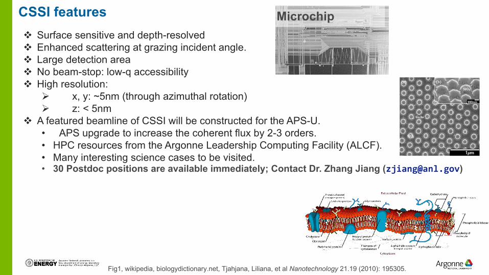
CSSI featuresv Surface sensitive and depth-resolvedv Enhanced scattering at grazing incident angle.v Large detection areav No beam-stop: low-q accessibilityv High resolution:
v A featured beamline of CSSI will be constructed for the APS-U.• APS upgrade to increase the coherent flux by 2-3 orders.• HPC resources from the Argonne Leadership Computing Facility (ALCF).• Many interesting science cases to be visited.• 30 Postdoc positions are available immediately; Contact Dr. Zhang Jiang ([email protected])
Microchip
Fig1, wikipedia, biologydictionary.net, Tjahjana, Liliana, et al Nanotechnology 21.19 (2010): 195305.
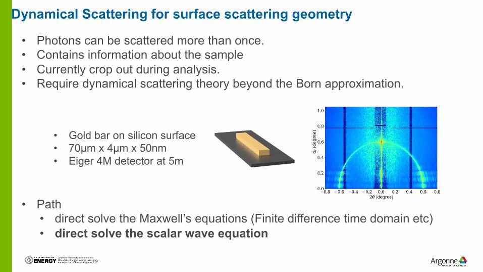
• Photons can be scattered more than once.• Contains information about the sample • Currently crop out during analysis.• Require dynamical scattering theory beyond the Born approximation.
Dynamical Scattering for surface scattering geometry
• Path• direct solve the Maxwell’s equations (Finite difference time domain etc)• direct solve the scalar wave equation
• Gold bar on silicon surface• 70µm x 4µm x 50nm• Eiger 4M detector at 5m
7
8
!"# = %&
"%#", !"
& = (&"%#
", !") = %&
"(#", !"
* = (&"(#
",
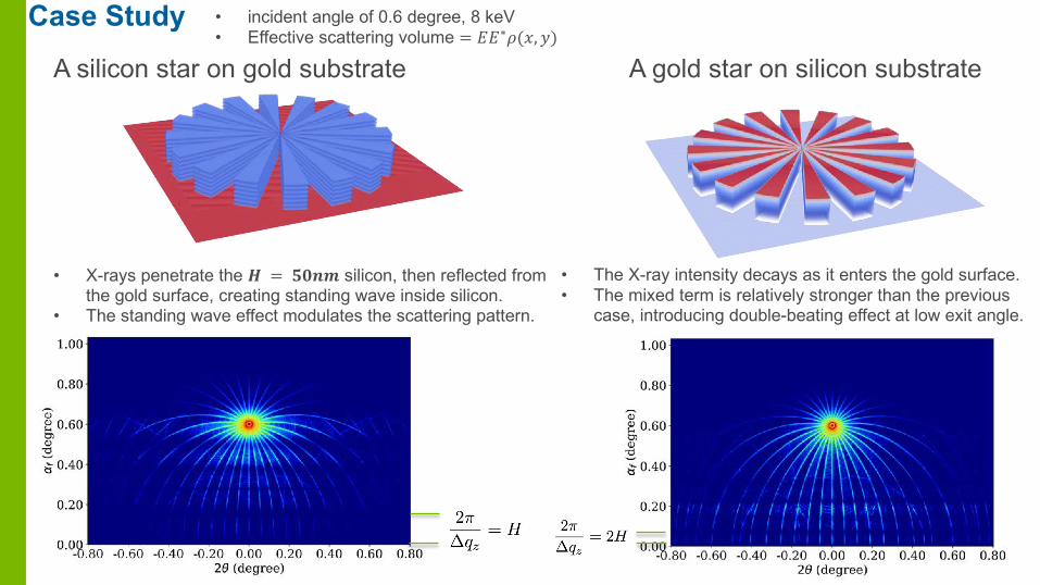
• DWBA takes the dynamical scattering effect in each layer into account, making the quantitative analysis of near-+, scattering effect possible.
• Eg. Reflectivity and Grazing incidence scattering.• However, the DWBA theory requires the averaging of in-plane electron density:
.̅" = ∬01 2,3 4243
∬ 4243, 5." 6, 7 = ." 6, 7 − .̅"
• This averaging breaks down when the sample is highly heterogeneous on mesoscale.
9"# = :"
& − :"#
9"& = :"
&; − :"# 9"
) = :"& − :"
#; 9"* = :"
&; − :"#;
<=<Ω
= ?@& ABC#
*
A"CD
EF#
∬!"B 5." G
FH91I⋅K<K
&
= ?@& ABC#
*
A"CD
EF#
∫ GFHM1,NI O<P∬!"
B 5." GFH91,QR
I ⋅KQR<6<7
&DWBA-Theory
Grid-based DWBA:• Three dimensional electric field intensity modulation• Divide the whole sample area into ("#,"%) small (and thus
more uniform) cells• For the ', ( th cell, centered at ()*+, ,*+)
• -*+ ./ = ∬2 #,%,34 5#5%∬5#5%
• Calculate the EFI for each cell from -*+(./)• Calculate the diffuse scattering field in each cell and
between nearby cells, add them with phase• 6 78, 2: = |∑*=>
?@AB∑+=>?CABD*+E*FGH + ∑JKLMN% D*+→*P+P E
*FGH|Q
DWBA :• One dimensional Electric field intensity modulation• - ./ = ∬2 #,%,34 5#5%
∬5#5%• Works for weak perturbation
Beam footprint
between cellsIn-cells
Grid-DWBA
footprint
• The dynamical scattering from one cell can be scattered again by a nearby cell.
Aurora, Argonne >1million (linpack) commission 2021, user facility
• Grid-based DBWA is able to capture the dynamical scattering effect in surface imaging setup.• Scattering theories beyond the Born Approximation are required for
• thick samples for ptychography• strong scattering objects for XPCI and CT
• We may have the computation power to implement dynamical scattering theories soon (now?).